JP5026738B2 - Display device - Google Patents
Display device Download PDFInfo
- Publication number
- JP5026738B2 JP5026738B2 JP2006151002A JP2006151002A JP5026738B2 JP 5026738 B2 JP5026738 B2 JP 5026738B2 JP 2006151002 A JP2006151002 A JP 2006151002A JP 2006151002 A JP2006151002 A JP 2006151002A JP 5026738 B2 JP5026738 B2 JP 5026738B2
- Authority
- JP
- Japan
- Prior art keywords
- common
- bus line
- voltage
- signal lines
- potential
- Prior art date
- Legal status (The legal status is an assumption and is not a legal conclusion. Google has not performed a legal analysis and makes no representation as to the accuracy of the status listed.)
- Active
Links
Images


Classifications
-
- G—PHYSICS
- G09—EDUCATION; CRYPTOGRAPHY; DISPLAY; ADVERTISING; SEALS
- G09G—ARRANGEMENTS OR CIRCUITS FOR CONTROL OF INDICATING DEVICES USING STATIC MEANS TO PRESENT VARIABLE INFORMATION
- G09G3/00—Control arrangements or circuits, of interest only in connection with visual indicators other than cathode-ray tubes
- G09G3/20—Control arrangements or circuits, of interest only in connection with visual indicators other than cathode-ray tubes for presentation of an assembly of a number of characters, e.g. a page, by composing the assembly by combination of individual elements arranged in a matrix no fixed position being assigned to or needed to be assigned to the individual characters or partial characters
- G09G3/34—Control arrangements or circuits, of interest only in connection with visual indicators other than cathode-ray tubes for presentation of an assembly of a number of characters, e.g. a page, by composing the assembly by combination of individual elements arranged in a matrix no fixed position being assigned to or needed to be assigned to the individual characters or partial characters by control of light from an independent source
- G09G3/36—Control arrangements or circuits, of interest only in connection with visual indicators other than cathode-ray tubes for presentation of an assembly of a number of characters, e.g. a page, by composing the assembly by combination of individual elements arranged in a matrix no fixed position being assigned to or needed to be assigned to the individual characters or partial characters by control of light from an independent source using liquid crystals
- G09G3/3611—Control of matrices with row and column drivers
- G09G3/3648—Control of matrices with row and column drivers using an active matrix
- G09G3/3655—Details of drivers for counter electrodes, e.g. common electrodes for pixel capacitors or supplementary storage capacitors
-
- G—PHYSICS
- G09—EDUCATION; CRYPTOGRAPHY; DISPLAY; ADVERTISING; SEALS
- G09G—ARRANGEMENTS OR CIRCUITS FOR CONTROL OF INDICATING DEVICES USING STATIC MEANS TO PRESENT VARIABLE INFORMATION
- G09G2300/00—Aspects of the constitution of display devices
- G09G2300/04—Structural and physical details of display devices
- G09G2300/0421—Structural details of the set of electrodes
- G09G2300/0434—Flat panel display in which a field is applied parallel to the display plane
Description
本発明は、表示装置に関し、特に、横電界駆動方式の液晶表示装置に適用して有効な技術に関するものである。 The present invention relates to a display device, and more particularly to a technique effective when applied to a horizontal electric field drive type liquid crystal display device.
従来、一対の基板の間に液晶材料を封入した液晶表示パネルを有する液晶表示装置には、たとえば、IPS方式のような横電界駆動方式のものがある。前記横電界駆動方式の液晶表示装置で用いられる液晶表示パネルは、前記一対の基板のうちの一方の基板に画素電極および共通電極(対向電極とも呼ばれる)が設けられている。 2. Description of the Related Art Conventionally, a liquid crystal display device having a liquid crystal display panel in which a liquid crystal material is sealed between a pair of substrates includes, for example, a lateral electric field driving method such as an IPS method. In a liquid crystal display panel used in the horizontal electric field drive type liquid crystal display device, a pixel electrode and a common electrode (also referred to as a counter electrode) are provided on one of the pair of substrates.
このとき、共通電極は、たとえば、基板に設けられた複数本の走査信号線または複数本の映像信号線と立体的に交差する網目状のコモン給電配線に接続されている。またこのとき、基板の表示領域の外側には、表示領域を囲む環状のコモンバスラインが設けられており、コモン給電配線はコモンバスラインに接続されている。 At this time, the common electrode is connected to, for example, a mesh-like common power supply wiring that three-dimensionally intersects with a plurality of scanning signal lines or a plurality of video signal lines provided on the substrate. At this time, an annular common bus line surrounding the display area is provided outside the display area of the substrate, and the common power supply wiring is connected to the common bus line.
前記コモン給電配線や対向電極に加えるコモン電位の電圧は、たとえば、タイミングコントローラーを有するプリント回路板に設けられたコモン電圧生成回路で生成される。そして、前記表示パネル(基板)に接続された複数個のプリント回路板から前記コモンバスラインに供給される。 The common potential voltage applied to the common power supply wiring and the counter electrode is generated by, for example, a common voltage generation circuit provided on a printed circuit board having a timing controller. And it supplies to the said common bus line from the some printed circuit board connected to the said display panel (board | substrate).
また、前記コモン給電配線は、前記複数本の走査信号線や前記複数本の映像信号線と立体的に交差しているので、交差している領域に生じる交差容量がノイズとなり、コモン給電配線(共通電極)の電位にばらつきが生じることがある。そのため、近年の液晶表示パネルでは、コモン給電配線の電位を測定し、生成するコモン電位の電圧にフィードバックすることで、コモン給電配線(共通電極)の電位にばらつきを低減している(たとえば、特許文献1を参照。)。
しかしながら、従来のフィードバック方法では、たとえば、コモン電位の電圧が入力される位置に近い場所でのコモン給電配線の電位を測定することが多い。そのため、測定しているコモン電位は、前記複数本の走査信号線や前記複数本の映像信号線と立体的に交差している領域に生じる交差容量などの影響が少なく、フィードバックにより電位を安定化させる際の精度が低いという問題があった。その結果、たとえば、表示領域において、コモン電位の電圧が入力される位置に近い場所と遠い場所で画質にむらが生じるなどの問題があった。 However, in the conventional feedback method, for example, the potential of the common power supply wiring is often measured near a position where the voltage of the common potential is input. Therefore, the measured common potential is less affected by the cross capacitance generated in the three-dimensionally intersecting area with the multiple scanning signal lines and the multiple video signal lines, and the potential is stabilized by feedback. There was a problem that the accuracy in making it low. As a result, there has been a problem that, for example, in the display region, the image quality is uneven in a place near and far from the position where the common potential voltage is input.
本発明の目的は、コモン給電配線に加えるコモン電位をフィードバックするときの精度を向上させることが可能な技術を提供することにある。 An object of the present invention is to provide a technique capable of improving accuracy when a common potential applied to a common power supply wiring is fed back.
本発明の前記ならびにその他の目的と新規な特徴は、本明細書の記述および添付図面によって明らかになるであろう。 The above and other objects and novel features of the present invention will be apparent from the description of this specification and the accompanying drawings.
本願において開示される発明のうち、代表的なものの概略を説明すれば、以下の通りである。 The outline of typical inventions among the inventions disclosed in the present application will be described as follows.
(1)一対の基板と、複数本の走査信号線と、前記複数本の走査信号線と交差する複数本の映像信号線と、前記複数本の走査信号線および前記複数本の映像信号線と交差する網目状のコモン給電配線と、表示領域の外側に該表示領域を囲む環状であり、かつ、前記コモン給電配線と電気的に接続されたコモンバスラインと、前記コモンバスラインおよび前記コモン給電配線に加えるコモン電位の電圧を生成するコモン電圧生成回路とを有する表示装置であって、前記コモンバスラインの電圧を前記コモン電圧生成回路にフィードバックするコモンセンシング配線を有し、前記コモンセンシング配線は、前記コモンバスラインの、前記コモン電位の電圧が加わる辺と反対側の辺に接続されており、かつ、前記基板に設けられた他の導電層と立体的に交差しない表示装置。
(2)前記(1)の表示装置において、前記コモン電圧生成回路は、該生成回路で生成したコモン電位の電圧と、該コモン電位の電圧を前記コモンバスラインおよびコモン給電配線に加えたときのコモン電位とを比較して、該生成回路で生成するコモン電位の電圧を調整するフィードバック回路を有する表示装置。
(1) a pair of substrates, a plurality of scanning signal lines, prior SL and a plurality of video signal lines for exchange difference and the scanning signal line a plurality of pre SL plurality of scanning signal lines and the plurality of video a mesh-like common supply line intersecting the signal lines, an annular surrounding the display area on the outside of the table display region, and a common bus line, wherein is common feed line electrically connected, before Symbol common a display device having a common voltage generation circuit for generating a voltage of the common potential applied to the bus line and the common power supply lines, have a common sensing line for feeding back the voltage before Kiko Monbasu lines to said common voltage generation circuit The common sensing wiring is connected to the side of the common bus line opposite to the side to which the voltage of the common potential is applied, and is connected to another conductive layer provided on the substrate. Display devices that do not intersect in.
(2) In the display device of (1), the common voltage generation circuit is configured to apply a common potential voltage generated by the generation circuit and the common potential voltage to the common bus line and the common power supply wiring. A display device including a feedback circuit that compares a common potential and adjusts a voltage of a common potential generated by the generation circuit.
(3)前記(2)の表示装置において、前記基板は、複数個のプリント回路板が接続されており、前記コモンセンシング配線は、前記コモンバスラインから前記コモン電圧生成回路までの経路において、複数回、前記プリント回路板を通り、かつ、前記プリント回路板上においても他の導電層と交差しない表示装置。 ( 3 ) In the display device of ( 2 ), a plurality of printed circuit boards are connected to the substrate , and a plurality of common sensing wirings are provided in a path from the common bus line to the common voltage generation circuit. times through the printed circuit board, and does not exchange difference and other conductive layers even in the printed circuit board on a display device.
(4)前記(2)の表示装置において、前記表示領域は、前記基板上に存在する矩形状の領域であり、前記コモンバスラインは、前記表示領域の1つの角で接する第1の辺と第2の辺からコモン電位の電圧が加わり、前記コモンセンシング配線は、前記コモンバスラインの前記第1の辺の反対側にある第3の辺に接続されており、前記コモンセンシング配線と前記コモンバスラインの接続部は、前記第2の辺からの距離が前記第3の辺の長さの半分以上である表示装置。
(5)前記(3)の表示装置において、前記表示領域は、前記基板上に存在する矩形状の領域であり、前記コモンバスラインは、前記表示領域の1つの角で接する第1の辺と第2の辺からコモン電位の電圧が加わり、前記コモンセンシング配線は、前記コモンバスラインの前記第1の辺の反対側にある第3の辺に接続されており、前記コモンセンシング配線と前記コモンバスラインの接続部は、前記第2の辺からの距離が前記第3の辺の長さの半分以上である表示装置。
(4) In the display device of the previous SL (2), the display area is a rectangular region that is present on the substrate, the common bus line, a first side in contact with one corner of the display region And a common potential voltage is applied from the second side, and the common sensing line is connected to a third side opposite to the first side of the common bus line, and the common sensing line and the second side The connection portion of the common bus line is a display device in which the distance from the second side is at least half of the length of the third side.
(5) In the display device according to (3), the display area is a rectangular area existing on the substrate, and the common bus line is connected to a first side that is in contact with one corner of the display area. A voltage of a common potential is applied from the second side, and the common sensing wiring is connected to a third side on the opposite side of the first side of the common bus line, and the common sensing wiring and the common The bus line connecting portion is a display device in which the distance from the second side is at least half the length of the third side.
(6)前記(1)の表示装置において、前記一対の基板の間には、液晶材料が封入されている表示装置。
( 6 ) The display device according to (1 ) , wherein a liquid crystal material is sealed between the pair of substrates .
本発明の表示装置は、表示パネルの基板に設けられたコモンバスラインおよびコモン給電配線の電位を測定し、その測定した電位に基づいてコモン電圧生成回路で生成するコモン電位の電圧を調整するフィードバック回路を有する。このとき、前記フィードバック回路にコモンバスラインおよびコモン給電配線の電位を伝えるコモンセンシング配線は、前記コモンバスラインの、前記コモン電位の電圧が加わる辺と反対側の辺に接続し、コモンバスラインからフィードバック回路にいたる経路において、前記基板に設けられた他の導電層と立体的に交差しないようにする。このようにすることで、コモン給電配線と走査信号線または映像信号線の交差領域に生じる交差容量の影響を反映した電位を測定でき、フィードバックの精度が向上する。 The display device of the present invention measures the potentials of the common bus line and the common power supply wiring provided on the substrate of the display panel, and adjusts the voltage of the common potential generated by the common voltage generation circuit based on the measured potential. It has a circuit. At this time, the common sensing wiring for transmitting the potential of the common bus line and the common power supply wiring to the feedback circuit is connected to the side of the common bus line opposite to the side to which the voltage of the common potential is applied, and from the common bus line. In the path leading to the feedback circuit, the other conductive layer provided on the substrate is prevented from crossing three-dimensionally. By doing so, the potential reflecting the influence of the cross capacitance generated in the cross region of the common power supply wiring and the scanning signal line or the video signal line can be measured, and the feedback accuracy is improved.
また、前記表示パネルは、たとえば、走査ドライバが実装されたCOFやデータドライバが実装されたCOFなどの複数個のプリント回路板が接続されている。そのため、コモンバスラインからフィードバック回路にいたる経路において、前記基板や前記プリント回路板の他の導電層と前記コモンセンシング配線が立体的に交差しないようにするには、たとえば、前記コモンセンシング配線が、前記コモンバスラインから前記コモン電圧生成回路までの経路において、複数回、前記プリント回路板を通るようにすればよい。 The display panel is connected to a plurality of printed circuit boards such as a COF mounted with a scanning driver and a COF mounted with a data driver. Therefore, in the path from the common bus line to the feedback circuit, in order to prevent the common sensing wiring from sterically intersecting with the other conductive layer of the substrate or the printed circuit board, for example, the common sensing wiring is: In the path from the common bus line to the common voltage generation circuit, the printed circuit board may be passed a plurality of times.
また、前記コモンバスラインは、たとえば、走査信号線の一方の端部がある辺と映像信号線の一方の端部がある辺のように、表示領域の1つの角で接する第1の辺と第2の辺からコモン電位の電圧が加わるのが一般的である。そのため、前記コモンセンシング配線を、たとえば、前記コモンバスラインの前記第1の辺の反対側にある第3の辺に接続する場合、前記コモンセンシング配線と前記コモンバスラインの接続部は、前記第2の辺からの距離が前記第3の辺の長さの半分以上となる位置にすることが望ましい。 In addition, the common bus line includes, for example, a first side that touches at one corner of the display area, such as a side having one end of the scanning signal line and a side having one end of the video signal line. In general, a common potential voltage is applied from the second side. Therefore, when connecting the common sensing wiring to, for example, a third side opposite to the first side of the common bus line, the connection part of the common sensing wiring and the common bus line is the first side. It is desirable that the distance from the second side be a position that is at least half the length of the third side.
また、本発明は、走査信号線または映像信号線と立体的に交差する網目状のコモン給電配線を有する表示装置であれば、どのような構成の表示装置にも適用できるが、特に、横電界型の液晶表示パネルを有する液晶表示装置に適用することが望ましい。 The present invention can be applied to a display device having any configuration as long as the display device has a mesh-like common power supply wiring that three-dimensionally intersects with a scanning signal line or a video signal line. It is desirable to apply to a liquid crystal display device having a liquid crystal display panel of a type.
以下、本発明について、図面を参照して実施の形態(実施例)とともに詳細に説明する。
なお、実施例を説明するための全図において、同一機能を有するものは、同一符号を付け、その繰り返しの説明は省略する。
Hereinafter, the present invention will be described in detail together with embodiments (examples) with reference to the drawings.
In all the drawings for explaining the embodiments, parts having the same function are given the same reference numerals and their repeated explanation is omitted.
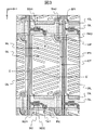
図1乃至図5は、本発明が適用される表示パネルの一構成例を示す模式図である。
図1は、液晶表示パネルを観察者側からみた模式平面図である。図2は、図1のA−A’線における模式断面図である。図3は、液晶表示パネルのTFT基板における表示領域の1画素の構成例を示す模式平面図である。図4は、図3のB−B’線における模式断面図である。図5は、図3のC−C’線における模式断面図である。
FIG. 1 to FIG. 5 are schematic views showing a structural example of a display panel to which the present invention is applied.
FIG. 1 is a schematic plan view of a liquid crystal display panel as viewed from the observer side. FIG. 2 is a schematic cross-sectional view taken along line AA ′ of FIG. FIG. 3 is a schematic plan view showing a configuration example of one pixel in the display region on the TFT substrate of the liquid crystal display panel. 4 is a schematic cross-sectional view taken along line BB ′ of FIG. FIG. 5 is a schematic cross-sectional view taken along the line CC ′ of FIG.
本発明は、複数本の走査信号線および複数本の映像信号線が設けられた基板に、走査信号線または映像信号線と立体的に交差するコモン給電配線が設けられている表示パネルに関するものである。このような表示パネルには、たとえば、IPS方式のような横電界駆動型の液晶表示パネルがある。 The present invention relates to a display panel in which a common power supply wiring three-dimensionally intersecting with a scanning signal line or a video signal line is provided on a substrate provided with a plurality of scanning signal lines and a plurality of video signal lines. is there. An example of such a display panel is a horizontal electric field drive type liquid crystal display panel such as an IPS system.
液晶表示パネルは、たとえば、図1および図2に示すように、一対の基板1,2の間に液晶材料3を封入した表示パネルである。このとき、一対の基板1,2は、表示領域DAの外側に環状に配置されたシール材4で接着されており、液晶材料3は、一対の基板1,2およびシール材4で囲まれた空間に封入されている。
For example, as shown in FIGS. 1 and 2, the liquid crystal display panel is a display panel in which a liquid crystal material 3 is sealed between a pair of
一対の基板1,2のうち、観察者側からみた外形寸法が大きい方の基板1は、一般に、TFT基板と呼ばれる。図1および図2では省略しているが、TFT基板1は、ガラス基板などの透明な基板の表面の上に、複数本の走査信号線と、絶縁層を介して前記複数本の走査信号線と立体的に交差する複数本の映像信号線が形成されている。そして、2本の隣接する走査信号線と2本の隣接する映像信号線で囲まれた領域が1つの画素領域に相当し、各画素領域に対してTFT素子や画素電極などが配置されている。また、TFT基板1と対をなす他方の基板2は、一般に、対向基板と呼ばれる。
Of the pair of
また、前記液晶表示パネルが、たとえば、IPS方式のような横電界駆動方式の場合、TFT基板1の画素電極と対向する共通電極(対向電極とも呼ばれる)は、TFT基板1側に設けられる。
Further, when the liquid crystal display panel is a lateral electric field driving method such as an IPS method, a common electrode (also referred to as a counter electrode) facing the pixel electrode of the
次に、横電界駆動方式の液晶表示パネルの表示領域DAの1画素の構成例について、図3乃至図5を参照して簡単に説明する。 Next, a configuration example of one pixel in the display area DA of the horizontal electric field drive type liquid crystal display panel will be briefly described with reference to FIGS.
横電界駆動方式の液晶表示パネルの場合、画素電極および共通電極は、TFT基板1側に設けられる。このとき、TFT基板1は、たとえば、図3乃至図5に示すように、ガラス基板SUBの表面に、x方向に延在する複数本の走査信号線GLが設けられており、走査信号線GLの上には、第1の絶縁層PAS1を介してy方向に延在し、複数本の走査信号線GLと立体的に交差する複数本の映像信号線DLが設けられている。そして、2本の隣接する走査信号線GLと2本の隣接する映像信号線DLによって囲まれた領域が1つの画素領域に相当する。
In the case of a horizontal electric field drive type liquid crystal display panel, the pixel electrode and the common electrode are provided on the
また、ガラス基板SUBの表面には、たとえば、画素領域毎に、平板状の共通電極CTが設けられている。このとき、x方向に並んだ各画素領域の共通電極CTは、走査信号線GLと並行した共通信号線CLによって電気的に接続されている。また、走査信号線GLからみて、共通信号線CLが設けられている方向と反対側には、共通電極CTと電気的に接続されている共通接続パッドCPが設けられている。 Further, on the surface of the glass substrate SUB, for example, a flat common electrode CT is provided for each pixel region. At this time, the common electrode CT of each pixel region arranged in the x direction is electrically connected by a common signal line CL parallel to the scanning signal line GL. A common connection pad CP electrically connected to the common electrode CT is provided on the side opposite to the direction in which the common signal line CL is provided when viewed from the scanning signal line GL.
また、第1の絶縁層PAS1の上には、映像信号線DLの他に、半導体層、ドレイン電極SD1、およびソース電極SD2が設けられている。このとき、半導体層は、たとえば、アモルファスシリコン(a−Si)を用いて形成されており、各画素領域に対して配置されるTFT素子のチャネル層SCとしての機能を持つものの他に、たとえば、走査信号線GLと映像信号線DLが立体的に交差する領域における走査信号線GLと映像信号線DLの短絡を防ぐもの(図示しない)がある。このとき、TFT素子のチャネル層SCとしての機能を持つ半導体層は、映像信号線DLに接続しているドレイン電極SD1とソース電極SD2の両方が接続されている。 In addition to the video signal line DL, a semiconductor layer, a drain electrode SD1, and a source electrode SD2 are provided on the first insulating layer PAS1. At this time, the semiconductor layer is formed using, for example, amorphous silicon (a-Si), and has a function as the channel layer SC of the TFT element disposed for each pixel region. There is one (not shown) that prevents a short circuit between the scanning signal line GL and the video signal line DL in a region where the scanning signal line GL and the video signal line DL intersect three-dimensionally. At this time, in the semiconductor layer having a function as the channel layer SC of the TFT element, both the drain electrode SD1 and the source electrode SD2 connected to the video signal line DL are connected.
また、映像信号線DLなどが形成された面(層)の上には、第2の絶縁層PAS2を介して画素電極PXが設けられている。画素電極PXは、画素領域毎に独立した電極であり、第2の絶縁層PAS2に設けられた開口部(スルーホール)TH1においてソース電極SD2と電気的に接続されている。また、共通電極CTと画素電極PXが、図3乃至図5に示したように、第1の絶縁層PAS1および第2の絶縁層PAS2を介して積層配置されている場合、画素電極PXは、スリットSLが設けられたくし歯形状の電極になっている。 On the surface (layer) on which the video signal line DL and the like are formed, the pixel electrode PX is provided via the second insulating layer PAS2. The pixel electrode PX is an independent electrode for each pixel region, and is electrically connected to the source electrode SD2 in an opening (through hole) TH1 provided in the second insulating layer PAS2. Further, when the common electrode CT and the pixel electrode PX are stacked via the first insulating layer PAS1 and the second insulating layer PAS2 as shown in FIGS. 3 to 5, the pixel electrode PX It is a comb-shaped electrode provided with a slit SL.
また、第2の絶縁層PAS2の上には、画素電極PXの他に、たとえば、走査信号線GLを挟んで上下に配置された2つの共通電極CTを電気的に接続するためのブリッジ配線BRが設けられている。このとき、ブリッジ配線BRは、走査信号線GLを挟んで配置された共通信号線CLおよび共通接続パッドCPとスルーホールTH2,TH3によって接続される。 Further, on the second insulating layer PAS2, in addition to the pixel electrode PX, for example, a bridge wiring BR for electrically connecting two common electrodes CT arranged above and below the scanning signal line GL. Is provided. At this time, the bridge wiring BR is connected to the common signal line CL and the common connection pad CP arranged across the scanning signal line GL by the through holes TH2 and TH3.
また、第2の絶縁層PAS2の上には、画素電極PXおよびブリッジ配線BRを覆うように配向膜5が設けられている。なお、図示は省略するが、対向基板2は、TFT基板1の配向膜5が設けられた面に対向するように配置される。
An alignment film 5 is provided on the second insulating layer PAS2 so as to cover the pixel electrode PX and the bridge wiring BR. Although not shown, the
以下、1画素の構成が図3乃至図5に示したよう構成の液晶表示パネルを有する液晶表示装置に本発明を適用した場合の構成例および作用効果について説明する。 Hereinafter, a configuration example and an operation effect when the present invention is applied to a liquid crystal display device having a liquid crystal display panel having a configuration of one pixel as shown in FIGS. 3 to 5 will be described.
図6は、本発明による一実施例の液晶表示装置の概略構成を示す模式図である。図7は、図6に示した領域P1におけるコモンバスラインの構成を説明するための模式平面図である。 FIG. 6 is a schematic diagram showing a schematic configuration of a liquid crystal display device according to an embodiment of the present invention. FIG. 7 is a schematic plan view for explaining the configuration of the common bus line in the region P1 shown in FIG.
本実施例の液晶表示装置において、液晶表示パネルのTFT基板1には、たとえば、図6表示領域DAを縦断するコモン給電配線および横断するコモン給電配線が網目状に配置されている。このとき、表示領域DAを縦断するコモン給電配線は、たとえば、ブリッジ配線BRおよび共通電極CTで構成される。また、表示領域を横断するコモン給電配線は、走査信号線GLに並行した共通信号線CLで構成される。また、表示領域DAに網目状に配置されたコモン給電配線は、表示領域DAの外側に環状に設けられたコモンバスラインCBLに接続されている。
In the liquid crystal display device of the present embodiment, for example, common power supply lines that traverse the display area DA in FIG. 6 and common power supply lines that traverse the display area DA are arranged in a mesh pattern on the
また、TFT基板1は、たとえば、1つの辺に、走査ドライバICが実装されたCOFなどのフレキシブルプリント回路板6Aが複数個接続されており、前記1つの辺と接するもう1つの辺に、データドライバICが実装されたCOFなどのフレキシブルプリント回路板6Bが複数個接続されている。また、フレキシブルプリント回路板6Bは、別のプリント回路板7に接続されている。また、プリント回路板7は、コモン電圧生成回路801やフィードバック回路802、タイミングコントローラー(図示しない)などを有する回路基板8に接続されている。
In addition, the
本実施例の液晶表示装置において、コモン電圧生成回路801で生成されたコモン電位の電圧は、プリント回路板7およびフレキシブルプリント回路板6A,6Bを介してTFT基板1のコモンバスラインCBLに供給される。またこのとき、コモンバスラインCBLには、コモンセンシング配線Csenが接続されている。コモンセンシング配線Csenは、コモンバスラインCBLおよびコモン給電配線の電位を測定し、コモン電圧生成回路801で生成するコモン電位の電圧を調整するためのものであり、フレキシブルプリント回路板6A,6Bおよびプリント回路板7を介して、フィードバック回路802に接続されている。
In the liquid crystal display device of this embodiment, the common potential voltage generated by the common
また、コモンセンシング配線Csenは、たとえば、図6に示すように、コモンバスラインCBLの4つの辺のうち、フレキシブルプリント回路板6Bを介してコモン電位の電圧が入力される辺の反対側の辺に接続する。またこのとき、コモンセンシング配線CsenとコモンバスラインCBLの接続位置P1は、たとえば、フレキシブルプリント回路板6Aからコモン電位の電圧が入力される辺からの距離が、コモンセンシング配線Csesが接続される辺の長さの半分以上になる領域AR1に設けることが望ましい。
Further, for example, as shown in FIG. 6, the common sensing wiring Csen is a side opposite to a side to which a common potential voltage is input via the flexible printed
なお、図6では、フレキシブルプリント回路板6Bからコモン電位の電圧が入力される辺の反対側の辺にコモンセンシング配線Csenを接続しているが、これに限らず、たとえば、フレキシブルプリント回路板6Aからコモン電位の電圧が入力される辺の反対側の辺にコモンセンシング配線Csenを接続してもよいことはもちろんである。その場合、コモンセンシング配線Csenは、フレキシブルプリント回路板6Bからコモン電位の電圧が入力される辺からの距離が、コモンセンシング配線Csesが接続される辺の長さの半分以上になる領域AR2においてコモンバスラインCBLに接続するのが望ましい。
In FIG. 6, the common sensing wiring Csen is connected to the side opposite to the side where the common potential voltage is input from the flexible printed
また、コモンセンシング配線Csenは、図7に示すように、コモンバスラインCBLの外側に、コモンバスラインCBLから分岐させて設け、コモンバスラインCBLの外周に沿ってTFT基板1のフレキシブルプリント回路板6Aが接続される領域まで引き回す。このとき、コモンセンシング配線Csenは、TFT基板1に設けられた他の導電層と立体的に交差しないように引き回す。そのため、コモンセンシング配線Csenは、たとえば、図6に示したように、フレキシブルプリント回路板6Aを経由させて、プリント回路板6Bまで導き、プリント回路板7を介してフィードバック回路802に接続させる。
Further, as shown in FIG. 7, the common sensing wiring Csen is provided outside the common bus line CBL and branched from the common bus line CBL, and the flexible printed circuit board of the
前記フィードバック回路802は、コモンセンシング配線Csenにより測定(取得)したコモンバスラインCBLおよびコモン給電配線の電位と、コモン電圧生成回路801で生成した基準電位を比較し、そのばらつきの度合いを算出する。そして、ばらつきが閾値以上である場合、たとえば、測定した電位と基準電位の差に基づき、コモン電圧生成回路801に、測定されるコモンバスラインCBLおよびコモン給電配線の電位が基準電位になるようなコモン電位の電圧を生成させる。
The
図8は、本実施例の液晶表示装置の作用効果を説明するための模式波形図である。なお、図8の波形図において、横軸は時間であり、縦軸は表示パネル上で測定したコモン電位(Vcom)である。 FIG. 8 is a schematic waveform diagram for explaining the function and effect of the liquid crystal display device of this embodiment. In the waveform diagram of FIG. 8, the horizontal axis represents time, and the vertical axis represents the common potential (Vcom) measured on the display panel.
本実施例の液晶表示装置において、従来の液晶表示装置のように、コモン電位の電圧が入力される位置に近い場所、たとえば、図6に示した領域P2におけるコモン電圧の波形は、たとえば、図8の上側に示した波形のようになる。領域P2はコモン電位の電圧が入力される位置に近いので、表示領域DAに網目状に設けられたコモン給電配線と走査信号線または映像信号線が立体的に交差する領域に生じる交差容量などの影響が少なく、ノイズの少ない波形になっている。 In the liquid crystal display device of this embodiment, the waveform of the common voltage in a location near the position where the common potential voltage is input, for example, the region P2 shown in FIG. The waveform is shown on the upper side of FIG. Since the area P2 is close to the position where the voltage of the common potential is input, the cross capacitance generated in the area where the common power supply wiring provided in a mesh shape in the display area DA and the scanning signal line or the video signal line cross three-dimensionally. The waveform is less affected and less noisy.
一方、本実施例の液晶表示装置のように、コモン電位の電圧が入力される位置から遠い場所、たとえば、図6に示した領域P1におけるコモン電位の波形は、たとえば、図8の下側に示した波形のようになる。つまり、本実施例の液晶表示装置では、表示領域DAに網目状に設けられたコモン給電配線と走査信号線または映像信号線が立体的に交差する領域に生じる交差容量などの影響でノイズがのっている波形に基づいてフィードバックすることができる。そのため、ノイズによる電位のばらつきを効率的に補正することができ、コモン給電配線(対向電極CT)の電位を精度よく安定化させることができる。 On the other hand, as in the liquid crystal display device of the present embodiment, the waveform of the common potential in a place far from the position where the common potential voltage is input, for example, the region P1 shown in FIG. It looks like the waveform shown. In other words, in the liquid crystal display device of this embodiment, noise is generated due to the influence of the cross capacitance generated in the area where the common power supply wiring provided in a mesh shape in the display area DA and the scanning signal line or the video signal line cross three-dimensionally. The feedback can be made based on the waveform. Therefore, potential variations due to noise can be corrected efficiently, and the potential of the common power supply wiring (counter electrode CT) can be stabilized with high accuracy.
以上、本発明を、前記実施例に基づき具体的に説明したが、本発明は、前記実施例に限定されるものではなく、その要旨を逸脱しない範囲において、種々変更可能であることはもちろんである。 The present invention has been specifically described above based on the above-described embodiments. However, the present invention is not limited to the above-described embodiments, and various modifications can be made without departing from the scope of the present invention. is there.
1…TFT基板
SUB…ガラス基板
GL…走査信号線
CL…共通信号線
CP…共通接続パッド
CT…共通電極(対向電極)
PAS1…第1の絶縁層
DL…映像信号線
SC…TFT素子のチャネル層(半導体層)
SD1…ドレイン電極
SD2…ソース電極
PAS2…第2の絶縁層
PX…画素電極
SL…スリット
BR…ブリッジ配線
TH1,TH2,TH3…スルーホール
2…対向基板
3…液晶材料
4…シール材
5…配向膜
6A,6B…フレキシブルプリント回路板
7…プリント回路板
8…回路基板
801…コモン電圧生成回路
802…フィードバック回路
1 ... TFT substrate SUB ... Glass substrate GL ... Scanning signal line CL ... Common signal line CP ... Common connection pad CT ... Common electrode (counter electrode)
PAS1 ... first insulating layer DL ... video signal line SC ... channel layer (semiconductor layer) of TFT element
SD1 ... Drain electrode SD2 ... Source electrode PAS2 ... Second insulating layer PX ... Pixel electrode SL ... Slit BR ... Bridge wiring TH1, TH2, TH3 ... Through
Claims (3)
当該基板の一方に、走査ドライバまたはデータドライバが搭載された複数のフレキシブルプリント基板と、複数本の走査信号線と、前記複数本の走査信号線と交差する複数本の映像信号線と、前記複数本の走査信号線および前記複数本の映像信号線と交差する網目状のコモン給電配線と、表示領域の外側に該表示領域を囲む環状であり、かつ、前記コモン給電配線と電気的に接続されたコモンバスラインとを有し、
前記コモンバスラインおよび前記コモン給電配線に加えるコモン電位の電圧を生成するコモン電圧生成回路とを有する表示装置であって、
前記コモン電圧生成回路は、該生成回路で生成したコモン電位の電圧と、該コモン電位の電圧を前記コモンバスラインおよびコモン給電配線に加えたときのコモン電位とを比較して、該生成回路で生成するコモン電位の電圧を調整するフィードバック回路を有し、
前記表示領域は、前記基板上に存在する矩形状の領域であり、
前記コモンバスラインは、前記表示領域の1つの角で接する第1の辺と第2の辺において、前記複数のフレキシブルプリント基板を介して複数個所からコモン電位の電圧が加わり、
前記コモンバスラインの電圧を前記コモン電圧生成回路にフィードバックするコモンセンシング配線を有し、
前記コモンセンシング配線は、前記コモンバスラインの前記第1の辺の反対側にある第3の辺に接続されており、前記コモンセンシング配線と前記コモンバスラインの接続部は、前記第2の辺からの距離が前記第3の辺の長さの半分以上であり、かつ、前記コモンセンシング配線が形成された前記基板に設けられた他の導電層と交差しないことを特徴とする表示装置。 A pair of substrates;
A plurality of flexible printed boards on which scanning drivers or data drivers are mounted on one of the substrates, a plurality of scanning signal lines, a plurality of video signal lines intersecting with the plurality of scanning signal lines, and the plurality of the plurality of scanning signal lines A mesh-like common power supply wiring intersecting with the plurality of scanning signal lines and the plurality of video signal lines, an annular shape surrounding the display area outside the display area, and electrically connected to the common power supply wiring and a common bus line was,
A display device having a common voltage generation circuit for generating a voltage of a common potential applied to the common bus line and the common power supply wiring;
The common voltage generation circuit compares the common potential voltage generated by the generation circuit with the common potential when the common potential voltage is applied to the common bus line and the common power supply wiring. A feedback circuit that adjusts the voltage of the common potential to be generated;
The display area is a rectangular area existing on the substrate,
The common bus line is applied with a common potential voltage from a plurality of locations via the plurality of flexible printed boards on the first side and the second side which are in contact with each corner of the display area.
A common sensing wiring for feeding back the voltage of the common bus line to the common voltage generation circuit;
The common sensing wiring is connected to a third side opposite to the first side of the common bus line, and a connection portion between the common sensing wiring and the common bus line is connected to the second side. The display device is characterized in that the distance from is not less than half the length of the third side and does not intersect with another conductive layer provided on the substrate on which the common sensing wiring is formed .
前記コモンセンシング配線は、前記コモンバスラインから前記コモン電圧生成回路までの経路において、複数回、前記プリント回路板を通り、かつ、前記プリント回路板上においても他の導電層と交差しないことを特徴とする請求項1に記載の表示装置。 The board is connected to a plurality of printed circuit boards,
The common sensing wiring passes through the printed circuit board a plurality of times in the path from the common bus line to the common voltage generation circuit, and does not intersect with other conductive layers on the printed circuit board. The display device according to claim 1 .
Priority Applications (2)
| Application Number | Priority Date | Filing Date | Title |
|---|---|---|---|
| JP2006151002A JP5026738B2 (en) | 2006-05-31 | 2006-05-31 | Display device |
| US11/752,320 US20070279355A1 (en) | 2006-05-31 | 2007-05-23 | Display Device |
Applications Claiming Priority (1)
| Application Number | Priority Date | Filing Date | Title |
|---|---|---|---|
| JP2006151002A JP5026738B2 (en) | 2006-05-31 | 2006-05-31 | Display device |
Publications (3)
| Publication Number | Publication Date |
|---|---|
| JP2007322580A JP2007322580A (en) | 2007-12-13 |
| JP2007322580A5 JP2007322580A5 (en) | 2008-12-25 |
| JP5026738B2 true JP5026738B2 (en) | 2012-09-19 |
Family
ID=38789506
Family Applications (1)
| Application Number | Title | Priority Date | Filing Date |
|---|---|---|---|
| JP2006151002A Active JP5026738B2 (en) | 2006-05-31 | 2006-05-31 | Display device |
Country Status (2)
| Country | Link |
|---|---|
| US (1) | US20070279355A1 (en) |
| JP (1) | JP5026738B2 (en) |
Families Citing this family (10)
| Publication number | Priority date | Publication date | Assignee | Title |
|---|---|---|---|---|
| JP4861242B2 (en) * | 2007-04-27 | 2012-01-25 | 株式会社 日立ディスプレイズ | Liquid crystal display |
| KR101451796B1 (en) * | 2008-03-27 | 2014-10-22 | 삼성디스플레이 주식회사 | Display appartus |
| KR101380228B1 (en) * | 2008-07-15 | 2014-04-03 | 엘지디스플레이 주식회사 | Array substrate for Chip on glass type liquid crystal display device |
| TWI425467B (en) * | 2010-02-03 | 2014-02-01 | Au Optronics Corp | Display capable of restraining ripple of common voltage |
| CN102650785A (en) * | 2012-03-02 | 2012-08-29 | 京东方科技集团股份有限公司 | Display panel and display device |
| KR101994971B1 (en) | 2012-05-16 | 2019-07-02 | 삼성디스플레이 주식회사 | Display device |
| TWI464731B (en) * | 2012-09-20 | 2014-12-11 | Au Optronics Corp | Display-driving structure and signal transmission method thereof, displaying device and manufacturing method thereof |
| KR102061875B1 (en) | 2013-08-28 | 2020-01-02 | 엘지디스플레이 주식회사 | Liquid Crystal Display Device |
| JP2015118193A (en) * | 2013-12-18 | 2015-06-25 | 株式会社ジャパンディスプレイ | Liquid crystal display device |
| CN210429262U (en) * | 2019-10-10 | 2020-04-28 | 北京京东方显示技术有限公司 | Display panel driving circuit, display panel and display device |
Family Cites Families (16)
| Publication number | Priority date | Publication date | Assignee | Title |
|---|---|---|---|---|
| JP2622190B2 (en) * | 1990-11-27 | 1997-06-18 | シャープ株式会社 | Liquid crystal display |
| GB9211283D0 (en) * | 1992-05-28 | 1992-07-15 | Philips Electronics Uk Ltd | Liquid crystal display devices |
| JP3288142B2 (en) * | 1992-10-20 | 2002-06-04 | 富士通株式会社 | Liquid crystal display device and driving method thereof |
| JP2872511B2 (en) * | 1992-12-28 | 1999-03-17 | シャープ株式会社 | Display device common electrode drive circuit |
| JPH06289817A (en) * | 1993-04-01 | 1994-10-18 | Sharp Corp | Method and circuit for driving display device |
| JPH09218388A (en) * | 1996-02-09 | 1997-08-19 | Hosiden Corp | Liquid crystal display device |
| US6532053B2 (en) * | 1996-12-18 | 2003-03-11 | Hitachi, Ltd. | Transverse electric field system liquid crystal display device suitable for improving aperture ratio |
| JPH1114968A (en) * | 1997-06-23 | 1999-01-22 | Sharp Corp | Common electrode driving circuit for display device |
| KR100271092B1 (en) * | 1997-07-23 | 2000-11-01 | 윤종용 | A liquid crystal display having different common voltage |
| JPH11119743A (en) * | 1997-10-17 | 1999-04-30 | Hoshiden Philips Display Kk | Liquid crystal display device |
| JP4142136B2 (en) * | 1997-10-31 | 2008-08-27 | ティーピーオー ホンコン ホールディング リミテッド | Liquid crystal display |
| KR100590746B1 (en) * | 1998-11-06 | 2006-10-04 | 삼성전자주식회사 | Liquid crystal display with different common voltages |
| KR100326880B1 (en) * | 1999-09-21 | 2002-03-13 | 구본준, 론 위라하디락사 | Liquid Crystal Display Device |
| KR100666119B1 (en) * | 1999-11-18 | 2007-01-09 | 삼성전자주식회사 | Liquid Crystal Display Device |
| JP3858590B2 (en) * | 2000-11-30 | 2006-12-13 | 株式会社日立製作所 | Liquid crystal display device and driving method of liquid crystal display device |
| JP2005157404A (en) * | 2005-02-10 | 2005-06-16 | Hitachi Ltd | Lateral electrolytic type liquid crystal display device suitable for improvement in numerical aperture |
-
2006
- 2006-05-31 JP JP2006151002A patent/JP5026738B2/en active Active
-
2007
- 2007-05-23 US US11/752,320 patent/US20070279355A1/en not_active Abandoned
Also Published As
| Publication number | Publication date |
|---|---|
| JP2007322580A (en) | 2007-12-13 |
| US20070279355A1 (en) | 2007-12-06 |
Similar Documents
| Publication | Publication Date | Title |
|---|---|---|
| JP5026738B2 (en) | Display device | |
| KR101500680B1 (en) | Display apparatus | |
| JP6979378B2 (en) | Display device with sensor | |
| KR101195688B1 (en) | Flexible substrate and electric circuit structure | |
| JP4861242B2 (en) | Liquid crystal display | |
| US20150138474A1 (en) | Liquid crystal display with ultra-narrow frame and cof packaging structure of driving circuit thereof | |
| JP2008032920A (en) | Liquid crystal display device | |
| JP6147533B2 (en) | Display device | |
| KR20170125187A (en) | Display device | |
| JP2019002960A (en) | Display device | |
| US10429970B2 (en) | Display device | |
| KR101148163B1 (en) | Thin film transistor substrate and display device having the same | |
| KR100825093B1 (en) | Liquid crystal device | |
| JP3965695B2 (en) | Liquid crystal display | |
| CN107436696B (en) | Touch panel and display device having the same | |
| JP4543725B2 (en) | Display device | |
| KR20080100580A (en) | Display substrate | |
| JP2014238464A (en) | Multi-faced circuit substrate for liquid-crystal display panel, and liquid-crystal display panel manufacturing method | |
| WO2019021927A1 (en) | Display panel | |
| JP2014206595A (en) | Liquid crystal display device | |
| JP5540502B2 (en) | Liquid crystal display panel and electronic device including the same | |
| US10976581B2 (en) | Display device | |
| JP2018049154A (en) | Display device | |
| KR20070106261A (en) | Liquid crystal display device | |
| KR20160047680A (en) | Horizontal electric field type liquid crystal display device |
Legal Events
| Date | Code | Title | Description |
|---|---|---|---|
| A521 | Request for written amendment filed |
Free format text: JAPANESE INTERMEDIATE CODE: A523 Effective date: 20081110 |
|
| A621 | Written request for application examination |
Free format text: JAPANESE INTERMEDIATE CODE: A621 Effective date: 20081110 |
|
| A711 | Notification of change in applicant |
Free format text: JAPANESE INTERMEDIATE CODE: A712 Effective date: 20110218 |
|
| RD03 | Notification of appointment of power of attorney |
Free format text: JAPANESE INTERMEDIATE CODE: A7423 Effective date: 20110218 |
|
| A131 | Notification of reasons for refusal |
Free format text: JAPANESE INTERMEDIATE CODE: A131 Effective date: 20110906 |
|
| A521 | Request for written amendment filed |
Free format text: JAPANESE INTERMEDIATE CODE: A523 Effective date: 20111027 |
|
| RD02 | Notification of acceptance of power of attorney |
Free format text: JAPANESE INTERMEDIATE CODE: A7422 Effective date: 20120330 |
|
| RD04 | Notification of resignation of power of attorney |
Free format text: JAPANESE INTERMEDIATE CODE: A7424 Effective date: 20120412 |
|
| TRDD | Decision of grant or rejection written | ||
| A01 | Written decision to grant a patent or to grant a registration (utility model) |
Free format text: JAPANESE INTERMEDIATE CODE: A01 Effective date: 20120612 |
|
| A01 | Written decision to grant a patent or to grant a registration (utility model) |
Free format text: JAPANESE INTERMEDIATE CODE: A01 |
|
| A61 | First payment of annual fees (during grant procedure) |
Free format text: JAPANESE INTERMEDIATE CODE: A61 Effective date: 20120621 |
|
| FPAY | Renewal fee payment (event date is renewal date of database) |
Free format text: PAYMENT UNTIL: 20150629 Year of fee payment: 3 |
|
| R150 | Certificate of patent or registration of utility model |
Ref document number: 5026738 Country of ref document: JP Free format text: JAPANESE INTERMEDIATE CODE: R150 Free format text: JAPANESE INTERMEDIATE CODE: R150 |
|
| R250 | Receipt of annual fees |
Free format text: JAPANESE INTERMEDIATE CODE: R250 |
|
| R250 | Receipt of annual fees |
Free format text: JAPANESE INTERMEDIATE CODE: R250 |
|
| R250 | Receipt of annual fees |
Free format text: JAPANESE INTERMEDIATE CODE: R250 |
|
| R250 | Receipt of annual fees |
Free format text: JAPANESE INTERMEDIATE CODE: R250 |
|
| R250 | Receipt of annual fees |
Free format text: JAPANESE INTERMEDIATE CODE: R250 |
|
| R250 | Receipt of annual fees |
Free format text: JAPANESE INTERMEDIATE CODE: R250 |
|
| R250 | Receipt of annual fees |
Free format text: JAPANESE INTERMEDIATE CODE: R250 |
|
| S531 | Written request for registration of change of domicile |
Free format text: JAPANESE INTERMEDIATE CODE: R313531 |
|
| S533 | Written request for registration of change of name |
Free format text: JAPANESE INTERMEDIATE CODE: R313533 |
|
| R350 | Written notification of registration of transfer |
Free format text: JAPANESE INTERMEDIATE CODE: R350 |
|
| R250 | Receipt of annual fees |
Free format text: JAPANESE INTERMEDIATE CODE: R250 |
|
| R250 | Receipt of annual fees |
Free format text: JAPANESE INTERMEDIATE CODE: R250 |
|
| S111 | Request for change of ownership or part of ownership |
Free format text: JAPANESE INTERMEDIATE CODE: R313117 |
|
| R350 | Written notification of registration of transfer |
Free format text: JAPANESE INTERMEDIATE CODE: R350 |