JP5020079B2 - Method and composition for providing a layer having uniform etching characteristics - Google Patents
Method and composition for providing a layer having uniform etching characteristics Download PDFInfo
- Publication number
- JP5020079B2 JP5020079B2 JP2007527859A JP2007527859A JP5020079B2 JP 5020079 B2 JP5020079 B2 JP 5020079B2 JP 2007527859 A JP2007527859 A JP 2007527859A JP 2007527859 A JP2007527859 A JP 2007527859A JP 5020079 B2 JP5020079 B2 JP 5020079B2
- Authority
- JP
- Japan
- Prior art keywords
- composition
- silicon
- component
- acrylic acid
- trimethylsiloxy
- Prior art date
- Legal status (The legal status is an assumption and is not a legal conclusion. Google has not performed a legal analysis and makes no representation as to the accuracy of the status listed.)
- Active
Links
Images


Classifications
-
- C—CHEMISTRY; METALLURGY
- C09—DYES; PAINTS; POLISHES; NATURAL RESINS; ADHESIVES; COMPOSITIONS NOT OTHERWISE PROVIDED FOR; APPLICATIONS OF MATERIALS NOT OTHERWISE PROVIDED FOR
- C09D—COATING COMPOSITIONS, e.g. PAINTS, VARNISHES OR LACQUERS; FILLING PASTES; CHEMICAL PAINT OR INK REMOVERS; INKS; CORRECTING FLUIDS; WOODSTAINS; PASTES OR SOLIDS FOR COLOURING OR PRINTING; USE OF MATERIALS THEREFOR
- C09D4/00—Coating compositions, e.g. paints, varnishes or lacquers, based on organic non-macromolecular compounds having at least one polymerisable carbon-to-carbon unsaturated bond ; Coating compositions, based on monomers of macromolecular compounds of groups C09D183/00 - C09D183/16
-
- B—PERFORMING OPERATIONS; TRANSPORTING
- B82—NANOTECHNOLOGY
- B82Y—SPECIFIC USES OR APPLICATIONS OF NANOSTRUCTURES; MEASUREMENT OR ANALYSIS OF NANOSTRUCTURES; MANUFACTURE OR TREATMENT OF NANOSTRUCTURES
- B82Y10/00—Nanotechnology for information processing, storage or transmission, e.g. quantum computing or single electron logic
-
- B—PERFORMING OPERATIONS; TRANSPORTING
- B82—NANOTECHNOLOGY
- B82Y—SPECIFIC USES OR APPLICATIONS OF NANOSTRUCTURES; MEASUREMENT OR ANALYSIS OF NANOSTRUCTURES; MANUFACTURE OR TREATMENT OF NANOSTRUCTURES
- B82Y40/00—Manufacture or treatment of nanostructures
-
- G—PHYSICS
- G03—PHOTOGRAPHY; CINEMATOGRAPHY; ANALOGOUS TECHNIQUES USING WAVES OTHER THAN OPTICAL WAVES; ELECTROGRAPHY; HOLOGRAPHY
- G03F—PHOTOMECHANICAL PRODUCTION OF TEXTURED OR PATTERNED SURFACES, e.g. FOR PRINTING, FOR PROCESSING OF SEMICONDUCTOR DEVICES; MATERIALS THEREFOR; ORIGINALS THEREFOR; APPARATUS SPECIALLY ADAPTED THEREFOR
- G03F7/00—Photomechanical, e.g. photolithographic, production of textured or patterned surfaces, e.g. printing surfaces; Materials therefor, e.g. comprising photoresists; Apparatus specially adapted therefor
- G03F7/0002—Lithographic processes using patterning methods other than those involving the exposure to radiation, e.g. by stamping
Description
発明の分野は、全体として構造物の微細加工に関する。より詳細には、本発明は、均一なエッチング特性を有する層を形成するための方法及びインプリント材料を対象とする。 The field of invention relates generally to microfabrication of structures. More particularly, the present invention is directed to a method and imprint material for forming a layer having uniform etching characteristics.
微細加工は、例えば、約数マイクロメートル以下のフィーチャを有する非常に小さな構造物の加工を含む。微細加工がかなり大きな影響を与えた1つの分野が集積回路の処理においてである。半導体処理産業が、基板上に形成される単位領域当たりの回路を増加させながら、より高い製品歩留まりを得るために努力し続けているので、微細加工はますます重要になっている。微細加工は、形成される構造物の最小のフィーチャ寸法を減少させながら、より優れたプロセス制御を提供する。微細加工が使われてきた他の開発領域には、バイオテクノロジー、光学技術、機械系等がある。 Microfabrication includes, for example, processing of very small structures having features of about a few micrometers or less. One area where microfabrication has had a significant impact is in the processing of integrated circuits. As the semiconductor processing industry continues to strive to obtain higher product yields while increasing the circuits per unit area formed on the substrate, microfabrication is becoming increasingly important. Microfabrication provides better process control while reducing the minimum feature size of the structure being formed. Other development areas where microfabrication has been used include biotechnology, optical technology, and mechanical systems.
典型的な微細加工技術が、Willsonらの特許文献1に示されている。Willsonらは、構造物内にレリーフ像を形成する方法を開示している。その方法には、転写層を有する基板を備えることが含まれる。転写層は重合可能な流体組成物で被覆されている。インプリント装置は、重合可能な流体と機械的に接触する。インプリント装置には、ランドとグルーブから形成されるレリーフ構造物が含まれる。重合可能な流体組成物は、そのレリーフ構造物を満たし、残りの厚さがランドに重なる重合可能な流体の厚さで決まる。次に、重合可能な流体組成物は、それを凝固し、かつ重合する条件下に置かれ、インプリント装置のレリーフ構造物に相補的なレリーフ構造物を含む転写層上に、凝固した高分子層を形成する。次に、インプリント装置は、インプリント装置内のレリーフ構造物の複製が凝固した高分子層内に形成されるように、凝固した高分子層から離される。転写層と凝固した高分子層は、レリーフ像が転写層内に形成されるように、凝固した高分子層に対して転写層を選択的にエッチングするための環境に置かれる。その後、従来のエッチング工程を、レリーフ構造物のパターンを基板に転写するために用いることができる。 A typical microfabrication technique is shown in US Pat. Willson et al. Disclose a method for forming a relief image in a structure. The method includes providing a substrate having a transfer layer. The transfer layer is coated with a polymerizable fluid composition. The imprint device is in mechanical contact with the polymerizable fluid. The imprint apparatus includes a relief structure formed from lands and grooves. The polymerizable fluid composition is determined by the thickness of the polymerizable fluid that fills the relief structure and the remaining thickness overlies the land. The polymerizable fluid composition is then placed under conditions to solidify and polymerize the polymerized solids on a transfer layer that includes a relief structure that is complementary to the relief structure of the imprint apparatus. Form a layer. The imprint apparatus is then separated from the solidified polymer layer such that a replica of the relief structure in the imprint apparatus is formed in the solidified polymer layer. The polymer layer solidified with the transfer layer is placed in an environment for selectively etching the transfer layer relative to the solidified polymer layer so that a relief image is formed in the transfer layer. A conventional etching process can then be used to transfer the relief structure pattern to the substrate.
従来のエッチング工程は、適切なマスク、例えばフォトレジストマスクを用いて層内に所望のパターンを形成していた。マスクは、通常、層上に堆積され、かつパターン化され、パターン化マスクを形成する。次に、パターン化マスクは、パターン化マスクを通して露出される層の部分を取り除くために、乾式エッチング工程でのイオン又は湿式エッチング技術での液体酸のような、エッチング剤に露出される。 Conventional etching processes have formed a desired pattern in the layer using an appropriate mask, such as a photoresist mask. A mask is usually deposited on the layer and patterned to form a patterned mask. The patterned mask is then exposed to an etchant, such as ions in a dry etching process or a liquid acid in a wet etching technique, to remove portions of the layer exposed through the patterned mask.
いかなるエッチング工程の望ましい特性も、エッチングされる表面にわたって均一のエッチング速度を得ることである。そのために、先行技術は、エッチング工程中にエッチング速度を制御する試みで満ちている。例えば、Haneyらの特許文献2は、反応性イオンエッチャにおいてエッチング速度均一性を達成する方法及び装置を開示している。反応性イオンエッチャは、プラズマが反応缶(reactor can)の上板から発生し、かつ局在磁界の結果として陰極全体に均一のエッチング速度分布を生成するために、陰極全体のエッチング速度を局在的に制御する局在磁界によって影響を受ける、真空チャンバ内で反応缶の陰極に配置された基板をエッチングするために、真空チャンバ内でプラズマを発生させる。磁石アレイを、局在磁界を提供するために、上板と真空チャンバの間に配置しても良い。磁石アレイは、複数の個別の磁石と、個別の磁石を定位置に保持する格子板を含む。 A desirable property of any etching process is to obtain a uniform etch rate across the surface being etched. To that end, the prior art is full of attempts to control the etch rate during the etching process. For example, Hanney et al., U.S. Pat. No. 6,057,077 discloses a method and apparatus for achieving etch rate uniformity in a reactive ion etcher. The reactive ion etcher localizes the etch rate across the cathode so that the plasma is generated from the top plate of the reactor can and produces a uniform etch rate distribution across the cathode as a result of the localized magnetic field. A plasma is generated in the vacuum chamber to etch the substrate located at the cathode of the reaction can in the vacuum chamber, which is affected by the local magnetic field that is controlled. A magnet array may be placed between the top plate and the vacuum chamber to provide a localized magnetic field. The magnet array includes a plurality of individual magnets and a grid plate that holds the individual magnets in place.
Daughertyらの特許文献3は、プラズマ処理システム中でイオンアシストエッチング処理のための方法及び装置を開示している。その発明の種々の形態によれば、高いエッジリングと、グルーブ付エッジリングと、RF結合エッジリングが、開示される。その発明は、基板(ウェハ)全体のエッチング速度均一性を改良する働きをする。その発明によって提供されるエッチング速度均一性の改良は、製造歩留まりを改良するだけでなく、費用効率が高く、かつ微粒子及び/又は重金属汚染の危険を冒さない。 Daugherty et al., US Pat. No. 5,677,077 discloses a method and apparatus for ion-assisted etching processing in a plasma processing system. According to various aspects of the invention, a high edge ring, a grooved edge ring, and an RF coupled edge ring are disclosed. The invention serves to improve the etch rate uniformity across the substrate (wafer). The improvement in etch rate uniformity provided by the invention not only improves manufacturing yield, but is also cost effective and does not run the risk of particulate and / or heavy metal contamination.
Meadorらの特許文献4は、改良されたエッチング速度を有する反射防止コーティング組成物を開示している。組成物は、全てが193nmの波長で光を吸収する、非多環カルボン酸染料及び非多環フェノール類染料によって反応したメタクリル酸グリシジルのような、ある種のアクリル系ポリマー及びコポリマーから調製される。
従って、処理を受けるインプリント材料のエッチング速度の制御が改良された、エッチング技術を提供することが必要である。 Accordingly, there is a need to provide an etching technique with improved control of the etching rate of the imprint material being processed.
本発明は、基板上に均一のエッチング特性を有する層を形成する方法及び組成物を含む。そのために、この方法は、基板上に、複数の成分の組成物として重合可能な液体を堆積させることを含む。各成分は、それに関連する蒸発速度を有する。重合可能な組成物は、次に凝固する。複数の成分のサブセットに関連した相対的蒸発速度が、所定の範囲内にあるように定められる。具体的には、本発明は、堆積した液体の凝固によって形成される、層内のエッチング不均一性が、層を形成する成分の相対的蒸発速度の関数であるという発見に基づく。結果として、組成物は複数の成分から形成され、そのサブセットが、ある時間的間隔に対して実質的に同一の蒸発速度を有する。これら及びその他の実施態様は、以下で更に十分に論じられる。 The present invention includes methods and compositions for forming a layer having uniform etching characteristics on a substrate. To that end, the method includes depositing a polymerizable liquid on the substrate as a multi-component composition. Each component has an evaporation rate associated with it. The polymerizable composition then solidifies. A relative evaporation rate associated with the subset of components is defined to be within a predetermined range. Specifically, the present invention is based on the discovery that etch non-uniformity within a layer, formed by solidification of the deposited liquid, is a function of the relative evaporation rate of the components that form the layer. As a result, the composition is formed from multiple components, a subset of which has substantially the same evaporation rate over a time interval. These and other embodiments are discussed more fully below.
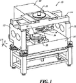
図1は、ブリッジ14と、その間に広がっているステージ支持体16を有する一対の離間したブリッジ支持体12を含む本発明の一実施形態に従ったリソグラフィックシステム10を描いている。ブリッジ14と、ステージ支持体16は離れている。ブリッジ14に結合されているのは、ブリッジ14からステージ支持体16に向かって延びているインプリントヘッド18である。インプリントヘッド18に面するようにステージ支持体16に配置されているのは、移動ステージ20である。移動ステージ20は、X、Y軸に沿ってステージ支持体16に対して動くように構成されており、かつ同様にZ軸に沿った移動も可能である。放射線源22は、化学線を移動ステージ20に入射させるようにシステム10に結合される。示したように、放射線源22は、ブリッジ14に結合され、かつ放射線源22に接続された発電機23を含む。
FIG. 1 depicts a
図1及び2の両方を参照すると、インプリントヘッド18に接続されているのは、パターン化モールド26を有するテンプレート24である。パターン化モールド26には、複数の離間した凹所28と凸部30によって形成された複数のフィーチャが含まれる。凸部30は幅W1を有し、かつ凹所28は幅W2を有し、その両方とも、Z軸を横切って延びる方向で測定される。複数のフィーチャは、移動ステージ20上に位置決めされる基板32に転写されるパターンの基礎を形成する元のパターンを形成している。そのために、インプリントヘッド18は、Z軸に沿って移動し、かつパターン化モールド26と基板32の間の距離「d」を変えるように構成されている。あるいは、又はインプリントヘッド18と共同して、移動ステージ20は、Z軸に沿ってテンプレート24を動かすことができる。このようにして、パターン化モールド26のフィーチャを、基板32の流動性領域にインプリントできる。以下で更に十分に論ずる。放射線源22は、パターン化モールド26が放射線源22と基板32の間に位置決めされるように置かれ、放射線源22によって発生する化学線が、パターン化モールド26を通って伝播する。その結果、パターン化モールド26が、化学線に実質的に透明な材料から製造されることが望ましい。パターン化モールド26が、製造できる典型的な材料には、用いられる化学線によって、溶融石英、石英、シリコン、有機ポリマー、シロキサンポリマー、ホウケイ酸ガラス、フルオロカーボンポリマー、金属、それらの組合せが含まれる。典型的なシステムは、78758テキサス州オースチン、1807−C Braker Lane、Suite 100に事業所を有するMolecular Imprints,Inc.からのIMPRIO 100(商標)という商品名で入手可能である。IMPRIO 100(商標)に関するシステム記述は、www.molecularimprints.comで入手可能である。
Referring to both FIGS. 1 and 2, connected to the
図2を参照すると、インプリント層34のような流動性領域が、表面対向テンプレート24の平面でないにせよ実質的に平滑なプロフィールを示す表面36の一部に形成される。本発明の一実施形態において、流動性領域は、以下で更に十分に論じるように、基板32上にインプリント材料の複数の離間した離散小滴38として堆積される。インプリント材料は、記録されたパターンを形成する、元のパターンの逆を内部に記録するために、選択的に重合され、かつ架橋される。パターン化モールド26上の複数のフィーチャは、パターン化モールド26の断面に狭間胸壁の形を与える凸部30と平行な方向に沿って伸長する凹所28として示される。しかしながら、凹所28と、凸部30は、集積回路を作成するために必要とされる、事実上いかなるフィーチャにも対応でき、かつ0.数ナノメートルくらいに小さくても良い。
With reference to FIG. 2, a flowable region, such as
図2及び3を参照すると、インプリント層34内に記録されたパターンは、パターン化モールド26との機械的接触によって部分的に生成される。そのために、距離「d」は、インプリント層34がパターン化モールド26と機械的に接触できるように減少させられ、表面36にわたるインプリント材料の連続形成によってインプリント層34を形成するように小滴38を広げる。一実施形態において、距離「d」は、インプリント層34の一部分46が凹所28に入り、かつ満たすように減少させられる。
With reference to FIGS. 2 and 3, the pattern recorded in the
本実施形態において、凸部30と重ね合わされるインプリント層34の一部分48は、所望の、通常は最小距離「d」に達した後に、残留し、厚さt1の一部分46と厚さt2の一部分48を残す。厚さt2は残留厚さと呼ばれる。厚さ「t1」と、「t2」は、用途によって、所望のいかなる厚さであってもよい。小滴38に含まれる全容積は、すなわちパターン化モールド26と、表面36によるインプリント材料の毛管引力と、インプリント材料の表面接着によって、所望の厚さt1とt2を得ながら、多量のインプリント材料が、パターン化モールド26と重ね合わされる表面36の領域を越え伸び出ることを回避又は最小に抑えるようになっていても良い。
In this embodiment, the
図2を参照すると、所望の距離「d」に達した後に、放射線源22は、インプリント材料を重合し、かつ架橋する化学線を生成し、凝固インプリント層134を形成する。インプリント層34の組成物は、流体インプリント材料から凝固材料に変形される。このことは、凝固インプリント層134に、図5に更に明瞭に示す、パターン化モールド26の表面50の形に合致する形を有する表面を与える。結果として凝固インプリント層134は、凹部52と、凸部54を有して形成される。凝固インプリント層134の形成後、パターン化モールド26と凝固インプリント層134が離れるように距離「d」を増加させる。通常、この工程は、基板32の異なる領域(図示せず)をパターン化するために、数回繰り返され、ステップ・アンド・リピート工程と呼ばれる。典型的なステップ・アンド・リピート工程は、本発明の譲受人に譲渡された、出願第10/194414号として2002年7月11日に出願され、「Step and Repeat Imprint Lithography」という題名を付された、米国特許出願公開第2004/0008334号明細書に開示されている。
Referring to FIG. 2, after reaching the desired distance “d”, the
このパターン化工程の利点は多方面にわたる。例えば、凸部54と、凹部52の間の厚さの差は、凝固インプリント層134内のパターンに対応するパターンの基板32内への形成を容易にする。具体的には、それぞれ凸部54と凹部52のt1とt2の間の厚さの差は、凹部52と重ね合わされる基板32の領域を露出させるのに必要な時間と比較して、凸部54と重ね合わされる基板32の領域を露出させるのには、より多くのエッチング時間を必要とする。従って、所与のエッチング工程に関して、エッチングは、凸部54と重ね合わされる領域よりも、凹部52と重ね合わされる基板32の領域で早く開始する。このことは、凝固インプリント層134内のパターンに対応する基板32内でのパターンの形成を容易にする。インプリント材料と、エッチング化学作用を適切に選択することによって、基板32に最終的に転写されるパターンの異なるフィーチャ間の関係寸法を、所望のように制御できる。そのために、凝固インプリント層134のエッチング特性が、所与のエッチング化学作用に関して実質的に均一であることが望まれる。
The benefits of this patterning process are numerous. For example, the difference in thickness between the convex portion 54 and the concave portion 52 facilitates formation of a pattern in the
結果として、インプリント材料の特性は、用いられる独特なパターン化工程に照らして、基板32を効率的にパターン化するために重要である。上述のように、インプリント材料は、離散し、かつ離間した複数の小滴38として基板32上に堆積する。小滴38の組み合わせた容積は、インプリント層34が形成されるべき表面36の領域にわたって、インプリント材料が、適切に分布するようになっている。この方法で、小滴38内のインプリント材料の全容積は、一旦、所望の距離「d」に達すると、重ね合わされるパターン化モールド26と基板32の部分の間に形成されたギャップにインプリント材料によって占められる総容積が小滴38内のインプリント材料の総容積と実質的に等しいように、得られるべき距離「d」を決める。結果として、インプリント層34は広げられと同時にかつパターン化され、パターンはその後に、化学線への露出によって実質的に設定される。堆積工程を容易にするために、すべての厚さt1が実質的に均一であり、かつすべての残留厚さt2が実質的に均一であるように、インプリント材料が、表面36にわたって小滴38内でインプリント材料が急速、かつ均等に広がることが望まれる。
As a result, the properties of the imprint material are important for efficiently patterning the
インプリント材料の典型的な組成物は、次のものからなる:
組成物1
アクリル酸イソボルニル
アクリロキシメチルビス(トリメチルシロキシ)メチルシラン
ジアクリル酸エチレングリコール
2−ヒドロキシ−2−メチル−1−フェニル−プロパン−1−オン
組成物2
アクリル酸イソボルニル
アクリロキシメチルトリス(トリメチルシロキシ)シラン
ジアクリル酸エチレングリコール
2−ヒドロキシ−2−メチル−1−フェニル−プロパン−1−オン
組成物3
アクリル酸イソボルニル
3−アクリロキシプロピルビス(トリメチルシロキシ)メチルシラン
ジアクリル酸エチレングリコール
2−ヒドロキシ−2−メチル−1−フェニル−プロパン−1−オン
組成物4
アクリル酸イソボルニル
3−アクリロキシプロピルトリス(トリメチルシロキシ)シラン
ジアクリル酸エチレングリコール
2−ヒドロキシ−2−メチル−1−フェニル−プロパン−1−オン
組成物5
アクリル酸イソボルニル
アクリロキシメチルビス(トリメチルシロキシ)メチルシラン
ジアクリル酸エチレングリコール
2−ヒドロキシ−2−メチル−1−フェニル−プロパン−1−オン
R1R2
組成物6
アクリル酸イソボルニル
アクリロキシメチルトリス(トリメチルシロキシ)シラン
ジアクリル酸エチレングリコール
2−ヒドロキシ−2−メチル−1−フェニル−プロパン−1−オン
R1R2
組成物7
アクリル酸イソボルニル
3−アクリロキシプロピルビス(トリメチルシロキシ)メチルシラン
ジアクリル酸エチレングリコール
2−ヒドロキシ−2−メチル−1−フェニル−プロパン−1−オン
R1R2
組成物8
アクリル酸イソボルニル
3−アクリロキシプロピルトリス(トリメチルシロキシ)シラン
ジアクリル酸エチレングリコール
2−ヒドロキシ−2−メチル−1−フェニル−プロパン−1−オン
R1R2
A typical composition of an imprint material consists of:
Composition 1
Isobornyl acryloxymethyl bis (trimethylsiloxy) methyl silane acrylate ethylene glycol 2-hydroxy-2-methyl-1-phenyl-propan-1-one composition 2
Isobornyl acryloxymethyl tris (trimethylsiloxy) silane acrylate ethylene glycol 2-hydroxy-2-methyl-1-phenyl-propan-1-one composition 3
Isobornyl acrylate 3-acryloxypropylbis (trimethylsiloxy) methylsilane ethylene glycol diacrylate 2-hydroxy-2-methyl-1-phenyl-propan-1-one composition 4
Isobornyl acrylate 3-acryloxypropyltris (trimethylsiloxy) silane diethylene glycol ethylene 2-hydroxy-2-methyl-1-phenyl-propan-1-
Isobornyl acryloxymethyl bis (trimethylsiloxy) methyl silane acrylate ethylene glycol 2-hydroxy-2-methyl-1-phenyl-propan-1-one R 1 R 2
Composition 6
Isobornyl acryloxymethyl tris (trimethylsiloxy) silane acrylate ethylene glycol 2-hydroxy-2-methyl-1-phenyl-propan-1-one R 1 R 2
Composition 7
Isobornyl acrylate 3-acryloxypropylbis (trimethylsiloxy) methylsilane ethylene glycol diacrylate 2-hydroxy-2-methyl-1-phenyl-propan-1-one R 1 R 2
Composition 8
Isobornyl acrylate 3-acryloxypropyltris (trimethylsiloxy) silane diacrylate ethylene glycol 2-hydroxy-2-methyl-1-phenyl-propan-1-one R 1 R 2
組成物1、2、3、4において、第1のシリコンのないアクリル酸塩、アクリル酸イソボルニルは、組成物の約42%になるが、その中に存在する量は、20〜60%の範囲でも良い。シリコン含有アクリル酸は、組成物1、2、3、4のいずれかの約37%になるが、その中に存在する量は、30〜50%の範囲でも良い。第2のシリコンのないアクリル酸塩、架橋剤ジアクリル酸エチレングリコールは、組成物1、2、3、4のいずれかの約18%になるが、存在する量は、10〜40%の範囲でも良い。開始剤、2−ヒドロキシ−2−メチル−1−フェニル−プロパン−1−オンは約0.5%〜5%であり、かつ組成物1〜4の架橋性と重合を促進させるために、紫外線に反応する。剥離特性の改良のために、組成物5、6、7、8は、それぞれ組成物1〜4の成分に加えて、組成物の約0.5%の界面活性剤R1R2を含む。組成物5、6、7、8の残りの成分は、界面活性剤の添加を補償するために、比例的に減少する。本発明の目的のために、界面活性剤は、その一端が疎水性である任意の分子と決められている。界面活性剤は、フッ素含有、例えば、フッ素鎖を含むか、又は界面活性剤の分子構造にいかなるフッ素も含まないかのいずれかであっても良い。
In compositions 1, 2, 3, and 4, the first silicon-free acrylate salt, isobornyl acrylate, is about 42% of the composition, but the amount present therein is in the range of 20-60%. But it ’s okay. The silicon-containing acrylic acid will be about 37% of any of compositions 1, 2, 3, 4 but the amount present therein may be in the range of 30-50%. The second silicone-free acrylate, the cross-linking agent ethylene glycol diacrylate, is about 18% of any of compositions 1, 2, 3, 4 but the amount present is also in the range of 10-40% good. The initiator, 2-hydroxy-2-methyl-1-phenyl-propan-1-one, is about 0.5% to 5%, and UV light is used to promote crosslinkability and polymerization of compositions 1-4. To react. For improved release properties,
典型的な界面活性剤は、R1R2[式中、R1=F(CF2CF2)Yであり、yは1〜7の範囲であり、かつR2=CH2CH2O(CH2CH2O)XHであり、ここでXは0〜15の範囲である]の一般的構造を有する、DUPONT(商標)から商品名ZONYL(登録商標)FS0−100として入手できる。しかしながら、他の界面活性剤が、F(CF2CF2)YCH2CH2O(CH2CH2O)XH界面活性剤の代わりに、又はそれに加えて組成物5、6、7、8に加えられてもよいことが理解されるべきである。追加の界面活性剤には、記号FLUORAD(登録商標)FC4432及び/又はFLUORAD(登録商標)FC4430の名で3M Companyから入手できるフッ素化高分子界面活性剤が含まれても良い。その上、他の紫外光開始剤が、2−ヒドロキシ−2−メチル−1−フェニル−プロパン−1−オンと併せて、又はその代わりに用いることができる。熱開始剤のような非光開始剤を用いてもよいことができることが理解されるべきである。結果として、架橋性と重合を促進させるために用いられる化学線は、性質が熱性、例えば赤外線である。
A typical surfactant is R 1 R 2 , where R 1 = F (CF 2 CF 2 ) Y , y is in the range of 1-7, and R 2 = CH 2 CH 2 O ( CH 2 CH 2 O) X H, where X is in the range of 0-15], available from DUPONT ™ under the trade name ZONYL® FS0-100. However, other surfactants may be used in place of or in addition to the F (CF 2 CF 2 ) Y CH 2 CH 2 O (CH 2 CH 2 O) X H surfactant,
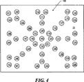
図4を参照すると、典型的な凝固インプリント層134の形成方法には、インプリント材料を表面36にわたって広げる時に、ガスの捕捉を最小限に抑えるために、複数の小滴をパターン100として堆積させることを含む。そのために、パターン100は、小滴101が最初に分配され、かつ小滴149が最後に分配される順番で、順次堆積した複数の小滴101〜149で形成される。しかしながら、凝固インプリント層134のエッチング特性は、逐次エッチング差(SED)と呼ばれる、滴分配シーケンス内の小滴の位置に応じて異なることが発見された。
Referring to FIG. 4, a typical method for forming a solidified
SEDは、凝固インプリント層134を形成する架橋かつ重合された成分の、凝固インプリント層134の領域にわたる変動に起因することが判定された。凝固インプリント層134内の成分変動は、インプリント材料が、蒸発のために流体状態にある間に起こることが発見された。具体的には、インプリント材料の組成物が、重合及び架橋される前に変化することが発見された。インプリント工程中に、蒸発は、数回の時間的間隔の間に起こる。小滴101の分配と、パターン100のモールド26との接触の間の時間的間隔は、約20秒である。これは、最大の蒸発が起こる間隔であると考えられている。この間隔の間に、インプリント材料の蒸発が起こり、インプリント材料の損失は、堆積と、モールド26との接触の間の間隔の長さに比例する。モールド26との接触後、第2の時間的間隔が、小滴101〜149を広げ、かつ基板32上に隣接シリコン含有層を形成するために必要である。通常約10秒の第2の時間的間隔の間に、インプリント材料の追加の蒸発が起こる。
It was determined that the SED was due to variations across the area of the solidified
本発明は、特定の重合可能な成分が所望の量で、凝固インプリント層134内に存在することを確実にすることによって、SEDを克服する。本実施例において、望ましい重合可能な成分は、シリコン含有アクリル酸成分と、IBOA及び架橋剤成分EDGAを含む非シリコン含有/シリコンのないアクリル酸成分とであり、それら全てがアクリル酸塩である。具体的には、凝固インプリント層134のエッチング特性の不均一性が、その領域にわたるシリコン含有量の変動によることが認識される。
The present invention overcomes SED by ensuring that certain polymerizable components are present in the desired amount in the solidified
シリコン含有アクリル酸塩が、組成物の残りの成分よりも速く蒸発した先行技術のシリコン含有組成物は、エッチング不均一性を示すことが発見された。このことは、図5と6を検討すると理解できる。図5において、前記先行技術のシリコン含有組成物から形成されるシリコン含有層150は、輪郭が実質的に平滑、かつ均一に見える。プラズマエッチング工程を層150に受けさせた後、不均一性が、エッチング層154内に現れる無数の凹型領域152によって観察できる。このことは、突出領域156のエッチング速度と比較して、凹型領域152に関連したより速いエッチング速度に起因する。凹型領域152のより速いエッチング速度は、突出領域156のシリコン含有量と比較して、低いシリコン量の存在に起因すると考えられる。層150内のシリコン含有量の不均一性は、エッチング層152の不均等なエッチングを招き、それは望ましくない。
It has been discovered that prior art silicon-containing compositions in which the silicon-containing acrylate has evaporated faster than the remaining components of the composition exhibit etch non-uniformity. This can be understood by examining FIGS. In FIG. 5, the silicon-containing
本発明は、望ましい成分が、所望の時間的間隔の間に、所望の蒸発速度を有する、インプリント材料の組成物を設定することによって、シリコン含有層内のエッチング不均一性を回避しないにせよ、軽減する。所望の成分の蒸発速度が無限周期で実質的に同じである組成物を提供することは可能であるが、不要であると判定された。むしろ、組成物1〜8の重合可能な成分が、堆積と化学線への露出との間の時間的間隔において所望の相対的蒸発速度を有するように選択される。組成物1〜4の残りの成分、すなわち光開始剤、2−ヒドロキシ−2−メチル−1−フェニル−プロパン−1−オンは、重合構造物の一部になるが、重合可能な成分と見なされない。従って、光開始剤、2−ヒドロキシ−2−メチル−1−フェニル−プロパン−1−オンは、結果として生じたインプリント層の構造特性に実質的に寄与せず、そのことは、蒸発速度を、アクリル酸成分の蒸発速度と一致させる必要性を最小限に抑える。同様に、組成物5〜8の残りの成分、すなわち光開始剤、2−ヒドロキシ−2−メチル−1−フェニル−プロパン−1−オンと、界面活性剤、RfCH2CH2O(CH2CH2O)XHとは、重合可能な成分と見なされない。更に、組成物1〜8の非重合可能な成分が、アクリル酸成分の蒸発速度よりも遅い速度で蒸発することが望ましい。 The present invention avoids etching non-uniformities in the silicon-containing layer by setting a composition of the imprint material in which the desired component has the desired evaporation rate during the desired time interval. To alleviate. Although it is possible to provide a composition in which the evaporation rate of the desired component is substantially the same over an infinite period, it has been determined to be unnecessary. Rather, the polymerizable components of compositions 1-8 are selected to have a desired relative evaporation rate in the time interval between deposition and exposure to actinic radiation. The remaining components of Compositions 1-4, i.e., the photoinitiator, 2-hydroxy-2-methyl-1-phenyl-propan-1-one, become part of the polymerized structure, but are considered polymerizable components. Not done. Thus, the photoinitiator, 2-hydroxy-2-methyl-1-phenyl-propan-1-one, does not substantially contribute to the structural properties of the resulting imprint layer, which reduces the evaporation rate. Minimize the need to match the evaporation rate of the acrylic acid component. Similarly, the remaining components of compositions 5-8, namely photoinitiator, 2-hydroxy-2-methyl-1-phenyl-propan-1-one, and surfactant, R f CH 2 CH 2 O (CH 2 CH 2 O) X H is not considered a polymerizable component. Furthermore, it is desirable that the non-polymerizable components of compositions 1-8 evaporate at a rate slower than the evaporation rate of the acrylic acid component.
図7を参照すると、組成物1の400pLの小滴内の特定成分の相対的蒸発速度を示す種々の曲線が示されている。特定成分は、次の通りである:ジアクリル酸エチレングリコール(EDGA)、アクリロキシメチルビス(トリメチルシロキシ)メチルシラン(AMBMS)、アクリル酸イソボルニル(IBOA)。400pLの小滴は、約82ミクロンの半径を有する400pLの小滴を提供するために、共通領域に各々が80pLの容積を有する複数の小滴の堆積によって形成された。組成物1の成分間の相対的蒸発速度は、0.1%/秒未満であることが示されており、それは20秒の間隔に関して2%未満に、かつ60秒の間隔にわたって約5%に変わる。組成物2〜8の重合可能な成分の同じような蒸発速度も発見された。結果として、組成物1〜8は、その重合可能な成分が、図3に示す、凝固インプリント層134の容積にわたって実質的に均一なシリコン密度を提供する、実質的に均一な蒸発速度を有することにおいて、望ましい特性を各々が持っている。具体的には、凝固インプリント層134には、凝固インプリント層134の所与の領域にわたって8重量%以上の所望のシリコン含有量が備えられる。凝固インプリント層134の任意の2つの領域間のシリコン含有量の最大重量変動は、5%以下であるべきである。
Referring to FIG. 7, various curves showing the relative evaporation rates of specific components within a 400 pL droplet of Composition 1 are shown. Specific components are as follows: ethylene glycol diacrylate (EDGA), acryloxymethylbis (trimethylsiloxy) methylsilane (AMBMS), isobornyl acrylate (IBOA). The 400 pL droplet was formed by the deposition of a plurality of droplets each having a volume of 80 pL in the common area to provide a 400 pL droplet having a radius of about 82 microns. The relative evaporation rate between the components of Composition 1 has been shown to be less than 0.1% / second, which is less than 2% for a 20 second interval and about 5% over a 60 second interval. change. Similar evaporation rates for the polymerizable components of compositions 2-8 were also discovered. As a result, Compositions 1-8 have a substantially uniform evaporation rate whose polymerizable components provide a substantially uniform silicon density across the volume of solidified
その上、組成物1〜8は、1〜20センチポアズの範囲であっても良く、5センチポアズ未満が好ましい、望ましい粘度を提供する。このことは、小滴分配技術を用いる堆積を容易にする。同様に、組成物1〜8は、破壊応力が、15MPa以上であるように所望の機械的強度を凝固インプリント層134を提供する。
Moreover, Compositions 1-8 provide the desired viscosity, which may be in the range of 1-20 centipoise, preferably less than 5 centipoise. This facilitates deposition using droplet dispensing techniques. Similarly, compositions 1-8 provide solidified
図2と8を参照すると、同様に、インプリント層34を上に形成する、平面でないにせよ平滑な表面を基板32に提供することが望ましい。そのために、基板32は、下塗り層96を含むことができる。基板32の表面36が、インプリント層34内に形成されるフィーチャ寸法と比較して粗く見える時、下塗り層96が有益であると証明された。下塗り層96は、同様に、とりわけインプリント層34を備える標準インターフェースを提供し、それにより、基板32が形成される、インプリント材料への各工程をカスタマイズする必要を減少させる。加えて、下塗り層96は、インプリント層34と同じ又は異なるエッチング特性を有する有機インプリント材料から形成できる。結果として、下塗り層96は、インプリント層34に対して優れた接着を示す、連続し、円滑な、かつ比較的欠陥のない表面を持つような方法で製造される。下塗り層96を形成するために使用する典型的な材料は、商品名DUV30J−6でRolla MissouriのBrewer Science,Inc.から入手可能である。下塗り層96は、通常、所望の表面プロフィールを提供することを容易にするために、ある厚さを備え、かつ基板32表面上で、位置合わせマークのようなパターンを検出するために用いられる光学感知装置に不透明ではない。
2 and 8, similarly, it is desirable to provide
図8、9を参照すると、予めパターン化された基板32の表面136上にインプリント層34が存在する時に、下塗り層196を堆積させること有益であることが発見された。そのために、下塗り層96のように、下塗り層196は、小滴分配技術、スピンオン技術等を含む、任意の公知の堆積方法を用いて堆積できる。更に、下塗り層96、196のいずれかの表面の平滑度を向上させるために、それを平面でないにせよ実質的に平滑な接触表面を有する、平坦化モールド80と接触させることが望ましい。
With reference to FIGS. 8 and 9, it has been discovered that it is beneficial to deposit a
凝固下塗り層96、196が、平坦化モールド80に接着する可能性を低くするために、低い表面エネルギーコーティング98で処理する。低い表面エネルギーコーティング98は、任意の公知の方法を使用して、適用できる。例えば、処理技術には、化学蒸着法、物理蒸着、原子層蒸着又は他の種々の技術、ろう付け等が含まれる。同じように、低い表面エネルギーコーティング(図示せず)が、図2に示す、モールド26に適用できる。
In order to reduce the likelihood that the solidified
上記界面活性剤と低い表面エネルギーコーティングに加えて、フッ素化添加剤が、インプリント材料の剥離性を改良するために用いることができる。フッ素化添加剤は、界面活性剤のように、インプリント材料の表面エネルギーよりも低い、それに関連した表面エネルギーを有する。前述のフッ素化添加剤を用いる典型的な方法が、Benderらによって、MULTIPLE IMPRINTING IN UV−BASED NANOIMPRINT LITHOGRAPHY:RELATED MATERIAL ISSUES、Microelectronic Engineering、pp.61〜62(2002)で論じられている。添加剤の低い表面エネルギーは、架橋され、かつ重合されたインプリント材料のモールド26、80への接着性を減少させるために、所望の剥離性を提供する。界面活性剤が、界面活性剤を含む組成物5〜8と併せて、又はその代わりに使用できることが理解されるべきである。
In addition to the surfactant and low surface energy coating, fluorinated additives can be used to improve the peelability of the imprint material. The fluorinated additive, like a surfactant, has a surface energy associated therewith that is lower than the surface energy of the imprint material. A typical method using the aforementioned fluorinated additives is described by Bender et al. In MULTIIPLE IMPRINTING IN UV-BASED NANOIMPRINT LITHOGRAPHY: RELATED MATERIAL ISSUES, Microelectronic Engineering, pp. 61-62 (2002). The low surface energy of the additive provides the desired peelability in order to reduce the adhesion of the crosslinked and polymerized imprint material to the
図5、10を参照すると、本発明によって提供される利益が、蒸発が層形成中に起こる他の技術を用いて形成された層にも同様に適用されることが理解されるべきである。凝固層234を形成するために用いることができる典型的な堆積技術には、スピンオン技術、レーザアシスト直接インプリント(LADI)技術等が含まれる。典型的なLADI技術は、Chouらによって、「Ultrafast and Direct Imprint of Nanostructure in Silicon」Nature、Col.417、pp.835〜837、2002年6月で開示されている。例えば、スピンオン技術を用いることにより、組成物1〜8のいずれでも、層234として基板32上に堆積できる。その後に、層234は、モールド26を用いてパターン化できる。パターン化される層234が、層234の異なる領域がパターン化され、その後順次凝固されるステップを用い、かつ技術を反復するならば、本発明の利益は際立つようになる。
Referring to FIGS. 5 and 10, it should be understood that the benefits provided by the present invention apply equally to layers formed using other techniques in which evaporation occurs during layer formation. Typical deposition techniques that can be used to form the solidified
上記本発明の実施形態は、典型的なものである。本発明の範囲内に留まりながら、多数の変更及び修正を、上記に説明した開示に行うことができる。例えば、前述の各組成物の成分比は、変えることができる。その上、本発明は、エッチング均一性を改良するための層内のシリコン含有量を制御することに対して論じたが、本発明は、接着力、優先的又は非優先的に、応力、厚さの均一性、粗さ、強度、密度等のような層の他の特性を改良するためにも同様に適用できる。従って、本発明の範囲は、上記記述によって限定されるべきでなく、その代わりに添付の特許請求の範囲を、その同等物の全範囲と共に参照して判定されるべきである。 The above-described embodiments of the present invention are typical. Numerous changes and modifications can be made to the disclosure described above while remaining within the scope of the invention. For example, the component ratio of each composition described above can be varied. Moreover, while the present invention has been discussed for controlling the silicon content in a layer to improve etch uniformity, the present invention is not limited to adhesive strength, preferential or non-preferential, stress, thickness, The same can be applied to improve other properties of the layer, such as thickness uniformity, roughness, strength, density, etc. Accordingly, the scope of the invention should not be limited by the above description, but should instead be determined by reference to the appended claims, along with their full scope of equivalents.
10 リソグラフィックシステム、18 インプリントヘッド、20 移動ステージ、22 放射線源、24 テンプレート、32 基板 10 Lithographic system, 18 Imprint head, 20 Moving stage, 22 Radiation source, 24 Template, 32 Substrate
Claims (25)
シリコン含有重合可能な成分と、シリコンのない重合可能な成分を含む複数の重合可能な成分と、
流体相状態と凝固相状態の間の、前記複数の重合可能な成分の位相状態の変化を容易にするための開始剤成分と、
を含み、
前記シリコン含有重合可能な成分は、アクリロキシメチルビス(トリメチルシロキシ)メチルシラン、またはアクリロキシメチルトリス(トリメチルシロキシ)シランを含み、
前記シリコンのない重合可能な成分は、アクリル酸エステルを含み、
前記複数の重合可能な成分間の相対的な蒸発速度は毎秒0.1%未満であることを特徴とする組成物。A composition for forming a layer having uniform etching characteristics on a substrate,
A plurality of polymerizable components including a silicon-containing polymerizable component and a silicon-free polymerizable component;
An initiator component for facilitating a change in phase state of the plurality of polymerizable components between a fluid phase state and a solidified phase state;
Including
The silicon-containing polymerizable component includes acryloxymethylbis (trimethylsiloxy) methylsilane, or acryloxymethyltris (trimethylsiloxy) silane,
The silicon-free polymerizable component includes an acrylate ester ,
A composition wherein the relative evaporation rate between the plurality of polymerizable components is less than 0.1% per second.
シリコン含有アクリル酸エステル成分と、第1と第2のシリコンのないアクリル酸エステル成分が含まれる複数のアクリル酸エステル成分と、
流体相状態と凝固相状態の間の、前記複数のアクリル酸エステル成分の位相状態の変化を容易にするための開始剤成分と、
を含み、
前記シリコン含有アクリル酸エステル成分は、アクリロキシメチルビス(トリメチルシロキシ)メチルシラン、またはアクリロキシメチルトリス(トリメチルシロキシ)シランを含み、
前記第1のシリコンのないアクリル酸エステル成分はアクリル酸イソボルニルを含み、
前記第2のシリコンのないアクリル酸エステル成分はジアクリル酸エチレングリコールを含み、
前記複数のアクリル酸エステル成分間の相対的な蒸発速度は毎秒0.1%未満であることを特徴とする組成物。A composition for forming a layer having uniform etching characteristics on a substrate,
A plurality of acrylic acid ester components including a silicon-containing acrylic acid ester component and first and second silicon-free acrylic acid ester components;
An initiator component for facilitating a change in phase state of the plurality of acrylate components between a fluid phase state and a solidified phase state;
Including
The silicon-containing acrylic ester component includes acryloxymethylbis (trimethylsiloxy) methylsilane, or acryloxymethyltris (trimethylsiloxy) silane,
Acrylic acid ester component without the first silicon includes isobornyl acrylate,
The second silicone-free acrylic ester component comprises ethylene glycol diacrylate;
A composition wherein the relative evaporation rate between the plurality of acrylic ester components is less than 0.1% per second.
アクリル酸イソボルニル成分と、
ジアクリル酸エチレングリコールと、
光開始剤成分と、
アクリロキシメチルビス(トリメチルシロキシ)メチルシラン、アクリロキシメチルトリス(トリメチルシロキシ)シラン、3−アクリロキシプロピルビス(トリメチルシロキシ)メチルシランから成るセットから選択されたシリコン含有アクリル酸エステル成分と、
を含み、
前記アクリル酸イソボルニル成分、前記ジアクリル酸エチレングリコール、および前記シリコン含有アクリル酸エステル成分を含む重合可能な成分間の相対的な蒸発速度は毎秒0.1%未満であることを特徴とする組成物。A composition for forming a layer having uniform etching characteristics on a substrate,
An isobornyl acrylate component;
Ethylene glycol diacrylate and
A photoinitiator component;
Acryloxymethyl bis (trimethylsiloxy) methylsilane, and acryloxymethyl tris (trimethylsiloxy) silane, 3-acryloxypropyl-bis (trimethylsiloxy) silicon-containing acrylic acid ester component selected from the set consisting of methylsilane,
Including
The isobornyl acrylate component, the ethylene glycol diacrylate, and relative evaporation rate of between polymerizable components containing the silicon-containing acrylic acid ester component composition and less than 0.1 per second%.
アクリル酸イソボルニル成分と、
ジアクリル酸エチレングリコールと、
光開始剤成分と、
3−アクリロキシプロピルトリス(トリメチルシロキシ)シランを含むシリコン含有アクリル酸エステル成分と、
を含み、
前記アクリル酸イソボルニル成分、前記ジアクリル酸エチレングリコール、および前記シリコン含有アクリル酸エステル成分を含む重合可能な成分間の相対的な蒸発速度は毎秒0.1%未満であることを特徴とする組成物。A composition for forming a layer having uniform etching characteristics on a substrate,
An isobornyl acrylate component;
Ethylene glycol diacrylate and
A photoinitiator component;
A silicon-containing acrylic acid ester component comprising 3-acryloxypropyltris (trimethylsiloxy) silane;
Including
The isobornyl acrylate component, the ethylene glycol diacrylate, and relative evaporation rate of between polymerizable components containing the silicon-containing acrylic acid ester component composition and less than 0.1 per second%.
Applications Claiming Priority (5)
| Application Number | Priority Date | Filing Date | Title |
|---|---|---|---|
| US10/919,062 US7282550B2 (en) | 2004-08-16 | 2004-08-16 | Composition to provide a layer with uniform etch characteristics |
| US10/919,224 US7939131B2 (en) | 2004-08-16 | 2004-08-16 | Method to provide a layer with uniform etch characteristics |
| US10/919,224 | 2004-08-16 | ||
| US10/919,062 | 2004-08-16 | ||
| PCT/US2005/027933 WO2006023297A1 (en) | 2004-08-16 | 2005-08-05 | Method and composition to provide a layer with uniform etch characteristics |
Publications (3)
| Publication Number | Publication Date |
|---|---|
| JP2008509815A JP2008509815A (en) | 2008-04-03 |
| JP2008509815A5 JP2008509815A5 (en) | 2011-03-03 |
| JP5020079B2 true JP5020079B2 (en) | 2012-09-05 |
Family
ID=35967849
Family Applications (1)
| Application Number | Title | Priority Date | Filing Date |
|---|---|---|---|
| JP2007527859A Active JP5020079B2 (en) | 2004-08-16 | 2005-08-05 | Method and composition for providing a layer having uniform etching characteristics |
Country Status (3)
| Country | Link |
|---|---|
| JP (1) | JP5020079B2 (en) |
| TW (1) | TWI291204B (en) |
| WO (1) | WO2006023297A1 (en) |
Families Citing this family (9)
| Publication number | Priority date | Publication date | Assignee | Title |
|---|---|---|---|---|
| US8142850B2 (en) * | 2006-04-03 | 2012-03-27 | Molecular Imprints, Inc. | Patterning a plurality of fields on a substrate to compensate for differing evaporation times |
| US8707890B2 (en) * | 2006-07-18 | 2014-04-29 | Asml Netherlands B.V. | Imprint lithography |
| WO2008154059A2 (en) | 2007-04-02 | 2008-12-18 | Regents Of The University Of California | Rotating frame gradient fields for mri and nmr in low polarizing magnetic fields |
| JP4908369B2 (en) * | 2007-10-02 | 2012-04-04 | 株式会社東芝 | Imprint method and imprint system |
| US20090212012A1 (en) * | 2008-02-27 | 2009-08-27 | Molecular Imprints, Inc. | Critical dimension control during template formation |
| NL2003875A (en) * | 2009-02-04 | 2010-08-05 | Asml Netherlands Bv | Imprint lithography method and apparatus. |
| JP5887871B2 (en) * | 2011-11-24 | 2016-03-16 | 富士通株式会社 | Film forming material and pattern forming method |
| JP6071255B2 (en) * | 2012-06-04 | 2017-02-01 | キヤノン株式会社 | Photocured material |
| US10892167B2 (en) * | 2019-03-05 | 2021-01-12 | Canon Kabushiki Kaisha | Gas permeable superstrate and methods of using the same |
Family Cites Families (5)
| Publication number | Priority date | Publication date | Assignee | Title |
|---|---|---|---|---|
| US5170192A (en) * | 1990-11-29 | 1992-12-08 | Pilkington Visioncare, Inc. | Oxygen permeable bifocal contact lenses and their manufacture |
| US6143433A (en) * | 1994-09-14 | 2000-11-07 | Mitsui Chemicals, Inc. | Organic electroluminescent device and process for producing the same |
| US20030124853A1 (en) * | 1998-06-25 | 2003-07-03 | Mitsubishi Materials Silicon Corporation | Anisotropic etching method and apparatus |
| ATE334809T1 (en) * | 2001-05-29 | 2006-08-15 | Essilor Int | METHOD FOR PRODUCING A COATED OPTICAL OBJECT |
| MY164487A (en) * | 2002-07-11 | 2017-12-29 | Molecular Imprints Inc | Step and repeat imprint lithography processes |
-
2005
- 2005-08-05 JP JP2007527859A patent/JP5020079B2/en active Active
- 2005-08-05 WO PCT/US2005/027933 patent/WO2006023297A1/en active Application Filing
- 2005-08-11 TW TW94127323A patent/TWI291204B/en not_active IP Right Cessation
Also Published As
| Publication number | Publication date |
|---|---|
| TW200612492A (en) | 2006-04-16 |
| TWI291204B (en) | 2007-12-11 |
| JP2008509815A (en) | 2008-04-03 |
| WO2006023297A1 (en) | 2006-03-02 |
Similar Documents
| Publication | Publication Date | Title |
|---|---|---|
| US7939131B2 (en) | Method to provide a layer with uniform etch characteristics | |
| JP5020079B2 (en) | Method and composition for providing a layer having uniform etching characteristics | |
| US7282550B2 (en) | Composition to provide a layer with uniform etch characteristics | |
| KR101121015B1 (en) | Capillary imprinting technique | |
| US7365103B2 (en) | Compositions for dark-field polymerization and method of using the same for imprint lithography processes | |
| KR101202653B1 (en) | Method to reduce adhesion between a conformable region and a pattern of a mold | |
| US8066930B2 (en) | Forming a layer on a substrate | |
| US7179396B2 (en) | Positive tone bi-layer imprint lithography method | |
| US8349241B2 (en) | Method to arrange features on a substrate to replicate features having minimal dimensional variability | |
| JP4942657B2 (en) | Polymerization techniques to attenuate oxygen inhibition of liquid coagulation and compositions therefor | |
| US20050156357A1 (en) | Planarization method of patterning a substrate | |
| US7858528B2 (en) | Positive tone bi-layer method | |
| US20030235787A1 (en) | Low viscosity high resolution patterning material |
Legal Events
| Date | Code | Title | Description |
|---|---|---|---|
| A621 | Written request for application examination |
Free format text: JAPANESE INTERMEDIATE CODE: A621 Effective date: 20080716 |
|
| A521 | Request for written amendment filed |
Free format text: JAPANESE INTERMEDIATE CODE: A523 Effective date: 20110111 |
|
| A871 | Explanation of circumstances concerning accelerated examination |
Free format text: JAPANESE INTERMEDIATE CODE: A871 Effective date: 20110111 |
|
| A977 | Report on retrieval |
Free format text: JAPANESE INTERMEDIATE CODE: A971007 Effective date: 20110126 |
|
| A975 | Report on accelerated examination |
Free format text: JAPANESE INTERMEDIATE CODE: A971005 Effective date: 20110324 |
|
| A131 | Notification of reasons for refusal |
Free format text: JAPANESE INTERMEDIATE CODE: A131 Effective date: 20110412 |
|
| A601 | Written request for extension of time |
Free format text: JAPANESE INTERMEDIATE CODE: A601 Effective date: 20110712 |
|
| A602 | Written permission of extension of time |
Free format text: JAPANESE INTERMEDIATE CODE: A602 Effective date: 20110720 |
|
| A521 | Request for written amendment filed |
Free format text: JAPANESE INTERMEDIATE CODE: A523 Effective date: 20110812 |
|
| A131 | Notification of reasons for refusal |
Free format text: JAPANESE INTERMEDIATE CODE: A131 Effective date: 20111206 |
|
| A521 | Request for written amendment filed |
Free format text: JAPANESE INTERMEDIATE CODE: A523 Effective date: 20120216 |
|
| TRDD | Decision of grant or rejection written | ||
| A01 | Written decision to grant a patent or to grant a registration (utility model) |
Free format text: JAPANESE INTERMEDIATE CODE: A01 Effective date: 20120522 |
|
| A01 | Written decision to grant a patent or to grant a registration (utility model) |
Free format text: JAPANESE INTERMEDIATE CODE: A01 |
|
| A61 | First payment of annual fees (during grant procedure) |
Free format text: JAPANESE INTERMEDIATE CODE: A61 Effective date: 20120612 |
|
| R150 | Certificate of patent or registration of utility model |
Ref document number: 5020079 Country of ref document: JP Free format text: JAPANESE INTERMEDIATE CODE: R150 Free format text: JAPANESE INTERMEDIATE CODE: R150 |
|
| FPAY | Renewal fee payment (event date is renewal date of database) |
Free format text: PAYMENT UNTIL: 20150622 Year of fee payment: 3 |
|
| R250 | Receipt of annual fees |
Free format text: JAPANESE INTERMEDIATE CODE: R250 |
|
| R250 | Receipt of annual fees |
Free format text: JAPANESE INTERMEDIATE CODE: R250 |
|
| R250 | Receipt of annual fees |
Free format text: JAPANESE INTERMEDIATE CODE: R250 |
|
| R250 | Receipt of annual fees |
Free format text: JAPANESE INTERMEDIATE CODE: R250 |
|
| R250 | Receipt of annual fees |
Free format text: JAPANESE INTERMEDIATE CODE: R250 |
|
| R250 | Receipt of annual fees |
Free format text: JAPANESE INTERMEDIATE CODE: R250 |
|
| R250 | Receipt of annual fees |
Free format text: JAPANESE INTERMEDIATE CODE: R250 |
|
| R250 | Receipt of annual fees |
Free format text: JAPANESE INTERMEDIATE CODE: R250 |
|
| R250 | Receipt of annual fees |
Free format text: JAPANESE INTERMEDIATE CODE: R250 |