JP5016225B2 - Array substrate, liquid crystal display panel having the same, and liquid crystal display device - Google Patents
Array substrate, liquid crystal display panel having the same, and liquid crystal display device Download PDFInfo
- Publication number
- JP5016225B2 JP5016225B2 JP2006007679A JP2006007679A JP5016225B2 JP 5016225 B2 JP5016225 B2 JP 5016225B2 JP 2006007679 A JP2006007679 A JP 2006007679A JP 2006007679 A JP2006007679 A JP 2006007679A JP 5016225 B2 JP5016225 B2 JP 5016225B2
- Authority
- JP
- Japan
- Prior art keywords
- electrode
- sub
- pixel
- pattern
- main
- Prior art date
- Legal status (The legal status is an assumption and is not a legal conclusion. Google has not performed a legal analysis and makes no representation as to the accuracy of the status listed.)
- Active
Links
- 239000000758 substrate Substances 0.000 title claims description 178
- 239000004973 liquid crystal related substance Substances 0.000 title claims description 86
- 238000003860 storage Methods 0.000 claims description 107
- 230000008878 coupling Effects 0.000 claims description 99
- 238000010168 coupling process Methods 0.000 claims description 99
- 238000005859 coupling reaction Methods 0.000 claims description 99
- 239000003990 capacitor Substances 0.000 claims description 62
- 239000010410 layer Substances 0.000 description 200
- 239000004065 semiconductor Substances 0.000 description 61
- XLOMVQKBTHCTTD-UHFFFAOYSA-N Zinc monoxide Chemical compound [Zn]=O XLOMVQKBTHCTTD-UHFFFAOYSA-N 0.000 description 36
- 239000010408 film Substances 0.000 description 32
- 239000010409 thin film Substances 0.000 description 31
- 230000007547 defect Effects 0.000 description 25
- 239000012535 impurity Substances 0.000 description 23
- 229910021417 amorphous silicon Inorganic materials 0.000 description 20
- 238000002161 passivation Methods 0.000 description 20
- 102100029136 Collagen alpha-1(II) chain Human genes 0.000 description 19
- 101000771163 Homo sapiens Collagen alpha-1(II) chain Proteins 0.000 description 19
- 102100033825 Collagen alpha-1(XI) chain Human genes 0.000 description 18
- 101000710623 Homo sapiens Collagen alpha-1(XI) chain Proteins 0.000 description 18
- 239000004020 conductor Substances 0.000 description 18
- 239000011787 zinc oxide Substances 0.000 description 18
- 239000000463 material Substances 0.000 description 15
- 238000007689 inspection Methods 0.000 description 12
- 238000000034 method Methods 0.000 description 10
- 229910052581 Si3N4 Inorganic materials 0.000 description 9
- AMGQUBHHOARCQH-UHFFFAOYSA-N indium;oxotin Chemical compound [In].[Sn]=O AMGQUBHHOARCQH-UHFFFAOYSA-N 0.000 description 9
- HQVNEWCFYHHQES-UHFFFAOYSA-N silicon nitride Chemical compound N12[Si]34N5[Si]62N3[Si]51N64 HQVNEWCFYHHQES-UHFFFAOYSA-N 0.000 description 9
- YVTHLONGBIQYBO-UHFFFAOYSA-N zinc indium(3+) oxygen(2-) Chemical compound [O--].[Zn++].[In+3] YVTHLONGBIQYBO-UHFFFAOYSA-N 0.000 description 9
- 229910004205 SiNX Inorganic materials 0.000 description 7
- 101100273664 Neurospora crassa (strain ATCC 24698 / 74-OR23-1A / CBS 708.71 / DSM 1257 / FGSC 987) ccp-1 gene Proteins 0.000 description 6
- 239000011651 chromium Substances 0.000 description 6
- 238000004519 manufacturing process Methods 0.000 description 6
- 229910052782 aluminium Inorganic materials 0.000 description 5
- XAGFODPZIPBFFR-UHFFFAOYSA-N aluminium Chemical compound [Al] XAGFODPZIPBFFR-UHFFFAOYSA-N 0.000 description 5
- 229910052751 metal Inorganic materials 0.000 description 5
- 239000002184 metal Substances 0.000 description 5
- ZOKXTWBITQBERF-UHFFFAOYSA-N Molybdenum Chemical compound [Mo] ZOKXTWBITQBERF-UHFFFAOYSA-N 0.000 description 4
- 230000015572 biosynthetic process Effects 0.000 description 4
- 239000010949 copper Substances 0.000 description 4
- 229910052750 molybdenum Inorganic materials 0.000 description 4
- 239000011733 molybdenum Substances 0.000 description 4
- 239000010936 titanium Substances 0.000 description 4
- VYZAMTAEIAYCRO-UHFFFAOYSA-N Chromium Chemical compound [Cr] VYZAMTAEIAYCRO-UHFFFAOYSA-N 0.000 description 3
- 229910052804 chromium Inorganic materials 0.000 description 3
- RYGMFSIKBFXOCR-UHFFFAOYSA-N Copper Chemical compound [Cu] RYGMFSIKBFXOCR-UHFFFAOYSA-N 0.000 description 2
- RTAQQCXQSZGOHL-UHFFFAOYSA-N Titanium Chemical compound [Ti] RTAQQCXQSZGOHL-UHFFFAOYSA-N 0.000 description 2
- 229910045601 alloy Inorganic materials 0.000 description 2
- 239000000956 alloy Substances 0.000 description 2
- 229910052802 copper Inorganic materials 0.000 description 2
- 230000002093 peripheral effect Effects 0.000 description 2
- 239000002356 single layer Substances 0.000 description 2
- 229910052715 tantalum Inorganic materials 0.000 description 2
- GUVRBAGPIYLISA-UHFFFAOYSA-N tantalum atom Chemical compound [Ta] GUVRBAGPIYLISA-UHFFFAOYSA-N 0.000 description 2
- 229910052719 titanium Inorganic materials 0.000 description 2
- WFKWXMTUELFFGS-UHFFFAOYSA-N tungsten Chemical compound [W] WFKWXMTUELFFGS-UHFFFAOYSA-N 0.000 description 2
- 229910052721 tungsten Inorganic materials 0.000 description 2
- 239000010937 tungsten Substances 0.000 description 2
- 229910000838 Al alloy Inorganic materials 0.000 description 1
- 229910052779 Neodymium Inorganic materials 0.000 description 1
- ATJFFYVFTNAWJD-UHFFFAOYSA-N Tin Chemical compound [Sn] ATJFFYVFTNAWJD-UHFFFAOYSA-N 0.000 description 1
- 206010047571 Visual impairment Diseases 0.000 description 1
- 230000003213 activating effect Effects 0.000 description 1
- 239000000919 ceramic Substances 0.000 description 1
- 238000000151 deposition Methods 0.000 description 1
- 238000010586 diagram Methods 0.000 description 1
- 230000000694 effects Effects 0.000 description 1
- 238000005516 engineering process Methods 0.000 description 1
- 239000011521 glass Substances 0.000 description 1
- 230000001939 inductive effect Effects 0.000 description 1
- 239000011810 insulating material Substances 0.000 description 1
- 238000009413 insulation Methods 0.000 description 1
- 238000000059 patterning Methods 0.000 description 1
- 238000000623 plasma-assisted chemical vapour deposition Methods 0.000 description 1
- 238000004528 spin coating Methods 0.000 description 1
- 239000000126 substance Substances 0.000 description 1
- 238000002834 transmittance Methods 0.000 description 1
Images


Classifications
-
- G—PHYSICS
- G02—OPTICS
- G02F—OPTICAL DEVICES OR ARRANGEMENTS FOR THE CONTROL OF LIGHT BY MODIFICATION OF THE OPTICAL PROPERTIES OF THE MEDIA OF THE ELEMENTS INVOLVED THEREIN; NON-LINEAR OPTICS; FREQUENCY-CHANGING OF LIGHT; OPTICAL LOGIC ELEMENTS; OPTICAL ANALOGUE/DIGITAL CONVERTERS
- G02F1/00—Devices or arrangements for the control of the intensity, colour, phase, polarisation or direction of light arriving from an independent light source, e.g. switching, gating or modulating; Non-linear optics
- G02F1/01—Devices or arrangements for the control of the intensity, colour, phase, polarisation or direction of light arriving from an independent light source, e.g. switching, gating or modulating; Non-linear optics for the control of the intensity, phase, polarisation or colour
- G02F1/13—Devices or arrangements for the control of the intensity, colour, phase, polarisation or direction of light arriving from an independent light source, e.g. switching, gating or modulating; Non-linear optics for the control of the intensity, phase, polarisation or colour based on liquid crystals, e.g. single liquid crystal display cells
- G02F1/133—Constructional arrangements; Operation of liquid crystal cells; Circuit arrangements
- G02F1/136—Liquid crystal cells structurally associated with a semi-conducting layer or substrate, e.g. cells forming part of an integrated circuit
- G02F1/1362—Active matrix addressed cells
- G02F1/136213—Storage capacitors associated with the pixel electrode
-
- G—PHYSICS
- G02—OPTICS
- G02F—OPTICAL DEVICES OR ARRANGEMENTS FOR THE CONTROL OF LIGHT BY MODIFICATION OF THE OPTICAL PROPERTIES OF THE MEDIA OF THE ELEMENTS INVOLVED THEREIN; NON-LINEAR OPTICS; FREQUENCY-CHANGING OF LIGHT; OPTICAL LOGIC ELEMENTS; OPTICAL ANALOGUE/DIGITAL CONVERTERS
- G02F1/00—Devices or arrangements for the control of the intensity, colour, phase, polarisation or direction of light arriving from an independent light source, e.g. switching, gating or modulating; Non-linear optics
- G02F1/01—Devices or arrangements for the control of the intensity, colour, phase, polarisation or direction of light arriving from an independent light source, e.g. switching, gating or modulating; Non-linear optics for the control of the intensity, phase, polarisation or colour
- G02F1/13—Devices or arrangements for the control of the intensity, colour, phase, polarisation or direction of light arriving from an independent light source, e.g. switching, gating or modulating; Non-linear optics for the control of the intensity, phase, polarisation or colour based on liquid crystals, e.g. single liquid crystal display cells
- G02F1/133—Constructional arrangements; Operation of liquid crystal cells; Circuit arrangements
- G02F1/1333—Constructional arrangements; Manufacturing methods
- G02F1/1343—Electrodes
- G02F1/134309—Electrodes characterised by their geometrical arrangement
- G02F1/134345—Subdivided pixels, e.g. for grey scale or redundancy
-
- G—PHYSICS
- G02—OPTICS
- G02F—OPTICAL DEVICES OR ARRANGEMENTS FOR THE CONTROL OF LIGHT BY MODIFICATION OF THE OPTICAL PROPERTIES OF THE MEDIA OF THE ELEMENTS INVOLVED THEREIN; NON-LINEAR OPTICS; FREQUENCY-CHANGING OF LIGHT; OPTICAL LOGIC ELEMENTS; OPTICAL ANALOGUE/DIGITAL CONVERTERS
- G02F1/00—Devices or arrangements for the control of the intensity, colour, phase, polarisation or direction of light arriving from an independent light source, e.g. switching, gating or modulating; Non-linear optics
- G02F1/01—Devices or arrangements for the control of the intensity, colour, phase, polarisation or direction of light arriving from an independent light source, e.g. switching, gating or modulating; Non-linear optics for the control of the intensity, phase, polarisation or colour
- G02F1/13—Devices or arrangements for the control of the intensity, colour, phase, polarisation or direction of light arriving from an independent light source, e.g. switching, gating or modulating; Non-linear optics for the control of the intensity, phase, polarisation or colour based on liquid crystals, e.g. single liquid crystal display cells
- G02F1/137—Devices or arrangements for the control of the intensity, colour, phase, polarisation or direction of light arriving from an independent light source, e.g. switching, gating or modulating; Non-linear optics for the control of the intensity, phase, polarisation or colour based on liquid crystals, e.g. single liquid crystal display cells characterised by the electro-optical or magneto-optical effect, e.g. field-induced phase transition, orientation effect, guest-host interaction or dynamic scattering
- G02F1/139—Devices or arrangements for the control of the intensity, colour, phase, polarisation or direction of light arriving from an independent light source, e.g. switching, gating or modulating; Non-linear optics for the control of the intensity, phase, polarisation or colour based on liquid crystals, e.g. single liquid crystal display cells characterised by the electro-optical or magneto-optical effect, e.g. field-induced phase transition, orientation effect, guest-host interaction or dynamic scattering based on orientation effects in which the liquid crystal remains transparent
- G02F1/1393—Devices or arrangements for the control of the intensity, colour, phase, polarisation or direction of light arriving from an independent light source, e.g. switching, gating or modulating; Non-linear optics for the control of the intensity, phase, polarisation or colour based on liquid crystals, e.g. single liquid crystal display cells characterised by the electro-optical or magneto-optical effect, e.g. field-induced phase transition, orientation effect, guest-host interaction or dynamic scattering based on orientation effects in which the liquid crystal remains transparent the birefringence of the liquid crystal being electrically controlled, e.g. ECB-, DAP-, HAN-, PI-LC cells
Landscapes
- Physics & Mathematics (AREA)
- Engineering & Computer Science (AREA)
- Nonlinear Science (AREA)
- Power Engineering (AREA)
- Microelectronics & Electronic Packaging (AREA)
- Mathematical Physics (AREA)
- Chemical & Material Sciences (AREA)
- Crystallography & Structural Chemistry (AREA)
- General Physics & Mathematics (AREA)
- Optics & Photonics (AREA)
- Liquid Crystal (AREA)
Description
本発明はアレイ基板、それを有する液晶表示パネル及び液晶表示装置に関し、より詳細には発生する画質不良を改善するためのアレイ基板、それを有する液晶表示パネル及び液晶表示装置に関する。 The present invention relates to an array substrate, a liquid crystal display panel having the same, and a liquid crystal display device.
一般的に、液晶表示装置LCDは各画素をスイッチングする薄膜トランジスタTFTが形成されたアレイ基板(またはTFT基板)と、共通電極が形成された対向基板(またはカラーフィルター基板)と、2つの間に密封された液晶層とで構成される。このような液晶表示装置では液晶層に電圧を印加して光の透過率を制御することで画像を表示する。
液晶表示装置は、液晶によって遮蔽されない方向のみに光が透過して画像を具現するので、相対的に他の表示装置に比べて視野角が狭いという短所がある。それにより、広視野角を実現するために垂直配向モード(以下、VAモードと称す)の液晶表示装置が開発された。
In general, a liquid crystal display device LCD is hermetically sealed between an array substrate (or TFT substrate) on which a thin film transistor TFT for switching each pixel is formed and a counter substrate (or color filter substrate) on which a common electrode is formed. Liquid crystal layer. In such a liquid crystal display device, an image is displayed by controlling the light transmittance by applying a voltage to the liquid crystal layer.
The liquid crystal display device has a disadvantage that a viewing angle is relatively narrow compared to other display devices because light is transmitted only in a direction that is not shielded by the liquid crystal and an image is realized. Accordingly, in order to realize a wide viewing angle, a vertical alignment mode (hereinafter referred to as VA mode) liquid crystal display device has been developed.
VAモードの液晶表示装置は、対向する面に対して垂直に配向処理された2つの基板と、2つの基板の間に密封されたネガティブ型の誘電率異方性を有する液晶層とで構成される。液晶層の液晶分子は垂直配向の性質を有する。
動作の際、2つの基板の間に電圧が印加されない時には、液晶分子が基板表面に対して略垂直方向に整列することでブラックを表示する。アレイ基板の制御電極とそれと連係されたカラーフィルター基板の共通電極に所定の電圧が印加される時には、液晶分子が基板表面に略水平方向に整列されホワイトを表示し、ホワイト表示のための電圧より小さい電圧が印加された時には、液晶分子が基板表面に対して斜めの方向に傾くように配向されグレーを表示する。このとき、グレー・スケールは液晶分子の平均配向に依存して変わる。
A VA mode liquid crystal display device is composed of two substrates that are aligned perpendicularly to opposing surfaces, and a liquid crystal layer having negative dielectric anisotropy sealed between the two substrates. The The liquid crystal molecules of the liquid crystal layer have a vertical alignment property.
In operation, when no voltage is applied between the two substrates, the liquid crystal molecules are aligned in a direction substantially perpendicular to the substrate surface, thereby displaying black. When a predetermined voltage is applied to the control electrode of the array substrate and the common electrode of the color filter substrate linked to the control electrode, the liquid crystal molecules are aligned in a substantially horizontal direction on the substrate surface to display white. When a small voltage is applied, the liquid crystal molecules are aligned so as to incline in an oblique direction with respect to the substrate surface and display gray. At this time, the gray scale changes depending on the average orientation of the liquid crystal molecules.
一方、液晶表示装置、特に中小型液晶表示装置には視野角を増加させるか、階調反転を抑制するためにPVAモード(Patterned Vertical Alignment)を採用するように構成されたLCD装置が使用される。PVAモードを採用する液晶表示装置は多重ドメインを画定するためにカラーフィルター基板にパターニングされた共通電極層とアレイ基板にパターニングされた画素電極層を有する。 On the other hand, an LCD device configured to adopt a PVA mode (Patterned Vertical Alignment) is used for a liquid crystal display device, particularly a medium-sized liquid crystal display device, in order to increase the viewing angle or suppress gradation inversion. . A liquid crystal display employing the PVA mode has a common electrode layer patterned on a color filter substrate and a pixel electrode layer patterned on an array substrate to define multiple domains.
最近では、視野角の改善のために互いに異なるピクセル電圧を有する分離された2つのピクセル電極領域、即ち、メインピクセルとサブピクセルを1つのピクセル領域内に形成している。このように、1つのピクセル領域にメインピクセルとサブピクセルを形成する技術をスーパーPVA(SPVA)と称する。
前記したスーパーPVA技術は、単位ピクセル内に1つのTFTを形成し、メインピクセルには直接的にデータ電圧を印加し、サブピクセルにはカップリングキャパシターを経由して間接的にデータ電圧を印加し、電圧差異を誘導する方法である。即ち、前記したカップリングキャパシタンスを用いてサブピクセルにデータ電圧を印加すると、サブピクセルの電圧は、カップリングキャパシター用配線とサブピクセルのピクセル電極間のカップリングキャパシタンスの形成によって間接的に誘導され、カップリングキャパシタンスとサブピクセル部分のストレージキャパシターによって決定される。
Recently, in order to improve the viewing angle, two separated pixel electrode regions having different pixel voltages, that is, a main pixel and a sub-pixel are formed in one pixel region. A technique for forming the main pixel and the sub-pixel in one pixel area in this way is referred to as Super PVA (SPVA).
The super PVA technology described above forms one TFT in a unit pixel, applies a data voltage directly to the main pixel, and indirectly applies a data voltage to the sub-pixel via a coupling capacitor. This is a method for inducing a voltage difference. That is, when a data voltage is applied to the sub-pixel using the coupling capacitance, the sub-pixel voltage is indirectly induced by forming a coupling capacitance between the coupling capacitor wiring and the pixel electrode of the sub-pixel, It is determined by the coupling capacitance and the storage capacitor in the sub-pixel part.
これにより、メインピクセルには相対的に高いキックバック電圧が印加されフリッカーのような画質不良が発生されるという問題点がある。 Accordingly, there is a problem that a relatively high kickback voltage is applied to the main pixel and an image quality defect such as flicker occurs.
本発明の技術的な課題は、このような点に鑑み出されたもので、本発明の目的はメインピクセルのキックバック電圧を減少させ、発生する画質不良を改善するために最適化されたPVAピクセル構造を有するアレイ基板を提供することにある。
本発明の他の目的は、前記したアレイ基板を有する液晶表示パネルを提供することにある。
The technical problem of the present invention has been devised in view of these points, and an object of the present invention is to optimize the PVA optimized for reducing the kickback voltage of the main pixel and improving the image quality defect that occurs. An object of the present invention is to provide an array substrate having a pixel structure.
Another object of the present invention is to provide a liquid crystal display panel having the above array substrate.
本発明のさらに他の目的は、前記したアレイ基板を有する液晶表示装置を提供することにある。 Still another object of the present invention is to provide a liquid crystal display device having the above-described array substrate.
前記した本発明の目的を実現するために一実施例によるアレイ基板は、スイッチング素子(例えば、TFTのようなトランジスタスイッチ)、メインピクセル部、カップリングキャパシター及びサブピクセル部を含む。前記スイッチング素子は互いに隣接するゲート配線とデータ配線によって画定される単位ピクセル領域に形成される。例えば、前記ピクセル領域は第1ゲート配線と隣接した第1データ配線によって画定され、また、第1ゲート配線に繋がる第2ゲート配線と、第1データ配線に繋がる第2データ配線によっても画定される。前記ゲート及びデータ配線は絶縁基板上に形成される。前記メインピクセル部は前記単位ピクセル領域の第1領域(例えば、中央領域)に形成される。前記カップリングキャパシターは前記スイッチング素子に接続される。前記サブピクセル部は前記カップリングキャパシターに接続され、前記単位ピクセル領域の第2領域(例えば、周辺領域)に形成される。 In order to realize the above-described object of the present invention, an array substrate according to an embodiment includes a switching element (eg, a transistor switch such as a TFT), a main pixel portion, a coupling capacitor, and a sub-pixel portion. The switching element is formed in a unit pixel region defined by a gate line and a data line adjacent to each other. For example, the pixel region is defined by a first data line adjacent to the first gate line, and is also defined by a second gate line connected to the first gate line and a second data line connected to the first data line. . The gate and the data line are formed on an insulating substrate. The main pixel part is formed in a first region (for example, a central region) of the unit pixel region. The coupling capacitor is connected to the switching element. The sub-pixel unit is connected to the coupling capacitor and formed in a second region (for example, a peripheral region) of the unit pixel region.
前記メインピクセル部には複数の開口パターンが形成されることを特徴とする。
前記サブピクセル部には複数の開口パターンが形成されることを特徴とする。
前記メインピクセル部は前記ゲート配線と平行し前記単位ピクセル領域を2分割する領域に形成されることを特徴とする。
前記メインピクセル部は、前記スイッチング素子に接続されることを特徴とする。前記メインピクセル部は下部に形成された第2カップリングパターンと、上部に形成され前記第2カップリングパターンとコンタクトするメイン電極とを含むことが望ましい。前記サブピクセル部は下部に形成された第1下部ストレージパターン、前記第1下部ストレージパターンとコンタクトする第1サブ電極、下部に形成された第2下部ストレージパターン及び前記第1サブ電極と分離されながら前記第2下部ストレージパターンとコンタクトする第2サブ電極を含むことが望ましい。
A plurality of opening patterns are formed in the main pixel portion.
A plurality of opening patterns are formed in the sub-pixel portion.
The main pixel portion may be formed in a region that is parallel to the gate wiring and divides the unit pixel region into two.
The main pixel unit is connected to the switching element. The main pixel unit may include a second coupling pattern formed in a lower portion and a main electrode formed in an upper portion and in contact with the second coupling pattern. The sub-pixel part is separated from the first lower storage pattern formed in the lower portion, the first sub electrode in contact with the first lower storage pattern, the second lower storage pattern formed in the lower portion, and the first sub electrode. Preferably, the second sub electrode is in contact with the second lower storage pattern.
このとき、前記メイン電極には単位ピクセル領域の第1ゲート配線と略平行方向の軸を中心として対称な2つのY字形状の開口パターンが形成されることを特徴とする。
前記第1サブ電極には前記メイン電極に形成されたY字形状の開口パターンの第1ゲート配線と平行でない分岐部のうちの一方と平行な2つの開口パターンが形成されることを特徴とする。
At this time, the main electrode is formed with two Y-shaped opening patterns that are symmetric about an axis substantially parallel to the first gate line of the unit pixel region.
The first sub-electrode is formed with two opening patterns parallel to one of the branch portions not parallel to the first gate wiring of the Y-shaped opening pattern formed in the main electrode. .
前記第2サブ電極には、前記メイン電極に形成されたY字形状の開口パターンの第1ゲート配線と平行でない分岐部のうちの他方と平行であり、前記第1ゲート配線に平行な軸を基準にして前記第1サブ電極に形成された開口パターンと対称である2つの開口パターンが形成されることを特徴とする。
前記した本発明の目的を実現するために他の実施例によるアレイ基板は、メインスイッチング素子、メインピクセル部、サブゲートライン、サブスイッチング素子及びサブピクセル部を含む。前記メインゲートランは単位ピクセル領域に形成される。前記メインスイッチング素子は前記メインゲートラインに接続される。前記メインピクセル部は前記メインスイッチング素子に接続され前記単位ピクセル領域の中央領域に形成される。前記サブゲートラインは前記単位ピクセル領域に形成される。前記サブスイッチング素子は前記サブゲートラインに接続される。前記サブピクセル部は前記単位ピクセル領域の残余領域に形成される。
The second sub-electrode is parallel to the other of the branch portions not parallel to the first gate wiring of the Y-shaped opening pattern formed on the main electrode, and has an axis parallel to the first gate wiring. Two opening patterns that are symmetrical to the opening pattern formed in the first sub-electrode with respect to the reference are formed.
In order to achieve the object of the present invention, an array substrate according to another embodiment includes a main switching element, a main pixel part, a sub-gate line, a sub-switching element, and a sub-pixel part. The main gate run is formed in a unit pixel region. The main switching element is connected to the main gate line. The main pixel unit is connected to the main switching element and formed in a central region of the unit pixel region. The sub gate line is formed in the unit pixel region. The sub-switching element is connected to the sub-gate line. The sub-pixel part is formed in a remaining area of the unit pixel area.
ここで、他の実施例によるアレイ基板は前記ゲートラインと平行に形成された第1下部ストレージパターンと、単位ピクセル領域を横方向に2分割する第1カップリングパターンとをさらに含み、前記第1カップリングパターンは単位ピクセルの端部領域で前記第1下部ストレージパターンと電気的に接続されることを特徴とする。
前記した本発明の他の目的を実現するために一実施例による液晶表示パネルは、上部基板、液晶層及び下部基板を含む。前記上部基板は共通電極層を具備する。前記下部基板は前記上部基板との結合により前記液晶層を収容するものであり、単位ピクセル領域の第1領域(例えば、中央領域)に形成されたメインピクセル部、スイッチング素子に接続されたカップリングキャパシター及び前記カップリングキャパシターに接続され、前記単位ピクセル領域の第2領域(例えば、周辺領域)に形成されたサブピクセル部を具備する。
Here, the array substrate according to another embodiment further includes a first lower storage pattern formed in parallel with the gate lines, and a first coupling pattern that divides a unit pixel region into two in the horizontal direction. The coupling pattern is electrically connected to the first lower storage pattern in an end region of the unit pixel.
In order to achieve the other object of the present invention, a liquid crystal display panel according to an embodiment includes an upper substrate, a liquid crystal layer, and a lower substrate. The upper substrate includes a common electrode layer. The lower substrate accommodates the liquid crystal layer by coupling with the upper substrate, and is coupled to a main pixel portion formed in a first region (for example, a central region) of a unit pixel region and a switching element. A sub-pixel unit connected to the capacitor and the coupling capacitor and formed in a second region (eg, a peripheral region) of the unit pixel region;
前記した本発明のさらにまたの目的を実現するために、一実施例による液晶表示装置はゲートライン、データライン、スイッチング素子、メインピクセル部、第1カップリングキャパシター、第1サブピクセル部、第2カップリングキャパシター及び第2サブピクセル部を含む。前記ゲートラインはゲート信号を伝達する。前記データラインはデータ信号を伝達する。前記スイッチング素子は前記ゲートライン及びデータラインに接続される。前記メインピクセル部は前記スイッチング素子に接続される。前記第1カップリングキャパシターは一端が前記スイッチング素子に接続される。前記第1サブピクセル部は前記第1カップリングキャパシターを経由して前記スイッチング素子に接続される。前記第2カップリングキャパシターは一端が前記スイッチング素子に接続される。前記第2サブピクセル部は前記第2カップリングキャパシターを経由して前記スイッチング素子に接続される。 In order to realize the further object of the present invention, a liquid crystal display according to an embodiment includes a gate line, a data line, a switching element, a main pixel unit, a first coupling capacitor, a first sub-pixel unit, a second A coupling capacitor and a second subpixel part are included. The gate line transmits a gate signal. The data line transmits a data signal. The switching element is connected to the gate line and the data line. The main pixel portion is connected to the switching element. One end of the first coupling capacitor is connected to the switching element. The first sub-pixel unit is connected to the switching element through the first coupling capacitor. One end of the second coupling capacitor is connected to the switching element. The second sub-pixel unit is connected to the switching element through the second coupling capacitor.
前記メインピクセル部は一端が前記スイッチング素子に接続され、他端が共通電圧に接続されたメイン液晶キャパシター及び一端が前記スイッチング素子に接続され、他端がストレージ電圧に接続されたメインストレージキャパシターを含むことを特徴とする。
前記第1サブピクセル部は、一端が前記第1カップリングキャパシターに接続され、他端が共通電圧に接続された第1液晶キャパシター及び一端が前記第1カップリングキャパシターに接続され、他端がストレージ電圧に接続された第1ストレージキャパシターを含むことを特徴とする。
The main pixel unit includes a main liquid crystal capacitor having one end connected to the switching element and the other end connected to a common voltage, and a main storage capacitor having one end connected to the switching element and the other end connected to a storage voltage. It is characterized by that.
The first subpixel unit has one end connected to the first coupling capacitor, the other end connected to a common voltage, and one end connected to the first coupling capacitor, and the other end connected to the storage. A first storage capacitor connected to the voltage is included.
前記第2サブピクセル部は、一端が前記第2カップリングキャパシターに接続され、他端が前記共通電圧に接続された第2液晶キャパシター及び一端が前記第2カップリングキャパシターに接続され、他端が前記ストレージ電圧に接続された第2ストレージキャパシターを含むことを特徴とする。
このようなアレイ基板、それを有する液晶表示パネル及び液晶表示装置によると、PVA構造でゲート配線とピクセル電極とが重畳され発生する追加的なゲート/ソース間キャパシターの面積をメインピクセルからサブピクセルに移転させることで、メインピクセルのキックバック電圧を減少させフリッカーのようにピクセルのRMS原因によって発生される画質不良を改善することができる。
The second sub-pixel unit has one end connected to the second coupling capacitor, the other end connected to the common voltage, one end connected to the second coupling capacitor, and the other end connected to the second coupling capacitor. A second storage capacitor connected to the storage voltage is included.
According to the array substrate, the liquid crystal display panel and the liquid crystal display device having the array substrate, the area of the additional gate / source capacitor generated by overlapping the gate wiring and the pixel electrode in the PVA structure is changed from the main pixel to the sub pixel. By transferring, the kickback voltage of the main pixel can be reduced, and the image quality defect caused by the RMS of the pixel like flicker can be improved.
以下、図面を参照して本発明の望ましい一実施例をより詳細に説明する。
ここで、紹介される実施例は当業者に本発明の思想が十分に伝達できるようにするために提供されたのである。図面において、多層(または膜)及び領域を明確に表現するために配線の幅や厚さを拡大して示している。全体的に、図面説明の際、観察者観点で説明し、層、膜、領域、板などの部分が他の部分の“上に”にあるとするとき、これは他の部分“すぐ上”にある場合に限らず、その中間にさらに他の部分がある場合も含む。反対に、ある部分が他の部分の“すぐ上”にあるという場合には中間に他の部分がないことを意味する。
Hereinafter, a preferred embodiment of the present invention will be described in detail with reference to the drawings.
The embodiments introduced here are provided so that those skilled in the art can fully communicate the idea of the present invention. In the drawings, the width and thickness of the wiring are shown enlarged in order to clearly represent the multilayer (or film) and the region. Overall, when explaining drawings, it is explained from an observer's point of view, and when a part such as a layer, a film, a region, or a plate is “on top” of another part, this means that the other part “just above” This includes not only the case where there is another part in the middle. On the other hand, when a part is “just above” another part, it means that there is no other part in the middle.
(実施例1)
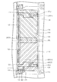
図1は本発明の第1実施例による液晶表示パネルを説明する平面図であり、図2は図1に示された液晶表示パネルをI−I’線に沿って切断した断面図である。特に、透過型アレイ基板を有する液晶表示パネルを図示する。
図1及び図2に示すように、本発明の第1実施例による液晶表示パネルはアレイ基板100、液晶層180及びアレイ基板100との結合されることにより液晶層180を収容するカラーフィルター基板190を含む。
Example 1
FIG. 1 is a plan view illustrating a liquid crystal display panel according to a first embodiment of the present invention, and FIG. 2 is a cross-sectional view of the liquid crystal display panel shown in FIG. 1 cut along the line II ′. In particular, a liquid crystal display panel having a transmissive array substrate is illustrated.
As shown in FIGS. 1 and 2, the liquid crystal display panel according to the first embodiment of the present invention is combined with the
アレイ基板100は、基板105の上に図における横方向に伸張されたゲート配線110、ゲート配線110から延長されたゲート電極112、ゲート配線110とは離間され単位ピクセル領域内でゲートライン110に平行である方向に形成された第1及び第2下部ストレージパターンSTL1、STL2及び単位ピクセル領域を図横方向に2分割する第1カップリングパターンCPLを含む。
The
アレイ基板100は、窒化珪素SiNxなどの材質からなり、ゲート配線110及びゲート電極112をカバーするゲート絶縁層113及びゲート電極112をカバーするアクティブ層114を含む。アクティブ層114は、a−Siのような半導体層、及び半導体層上に形成されたn+a−Siのような半導体不純物層を含む。
アレイ基板100は、縦方向に伸張されたソース配線120、ソース配線120から延長されたソース電極122及びソース電極122と一定間隔離間するドレイン電極123を含む。ここで、ゲート電極112、半導体層と半導体不純物層からなるアクティブ層114、ソース電極122及びドレイン電極123は薄膜トランジスタTFTを画定する。
The
The
アレイ基板100は、ドレイン電極123から延長された第1上部ストレージパターン124、単位ピクセル領域の図左側に形成され、ドレイン電極123から延長された第1延長パターン125、第1延長パターン125に接続された第2カップリングパターン126、単位ピクセル領域の図左側に形成され、第1延長パターン125に接続された第2延長パターン127及び第2延長パターン127に接続された第2上部ストレージパターン128を含む。
The
ゲート配線110やソース配線120は、単一層または二重層などで形成することができる。単一層で形成する場合には、アルミニウム(Al)やアルミニウム(Al)−ネオジウム(Nd)合金で形成することができ、二重層で形成する場合にはクロム(Cr)、モリブデン(Mo)またはモリブデン合金膜などの物理/化学的特性の優れた物質を下部層として形成し、アルミニウム(Al)またはアルミニウム合金などの非抵抗の低い物質を上部層として形成する。
The
アレイ基板100は、薄膜トランジスタTFTを覆いながらドレイン電極126の一部を露出するように順に積層したパッシベーション層130と有機絶縁層132とを含む。パッシベーション層130と有機絶縁層132は、ソース電極122とドレイン電極123との間のアクティブ層114をカバーして保護する役割、及び薄膜トランジスタTFTとピクセルデータ部140を絶縁する役割を果たす。アクティブ層114は半導体層と半導体層上に形成された半導体不純物層を含む。
The
有機絶縁層132の高さ調節を通じて液晶層180の厚さ(液晶層のセルギャップ)を調節することもできる。他の実施例においては、パッシベーション層130を省略することもできる。
アレイ基板100は薄膜トランジスタ(TFT)のドレイン電極123にコンタクトホールを通じて電気的に接続され開口されたパターン形状を有するピクセル電極部140を含む。
Through adjustment of the height of the organic insulating
The
具体的に、ピクセルデータ部140は第2カップリングパターン126とコンタクトするメイン電極144、第1下部ストレージパターンSTL1とコンタクトする第1サブ電極142、第1サブ電極142と分離され第2下部ストレージパターンとコンタクトする第2サブ電極146を含む。
メイン電極144には単位ピクセル領域を図横方向の軸を中心として対称である2つのY字形状の開口パターンが形成される。対称に構成されるY字形状の分岐部(ゲート配線と平行でない部分)は90°の角度を有する2つの分岐部で構成される。第1サブ電極142には、Y字形状の分岐部の一方と平行である2つの開口パターンが形成される。第2サブ電極146には、Y字形状の分岐部の他方と平行であり、図横方向の軸を基準として、第1サブ電極142に形成された開口パターンと対称な2つの開口パターンが形成される。メイン電極144、第1及び第2サブ電極142、146に複数の開口パターンを形成するのは、この後カラーフィルター基板との結合により収容される液晶層のドメインを複数個に分割するためである。
Specifically, the
The
メイン電極144、第1及び第2サブ電極142、146は透明な導電性物質で形成される。このような透明な導電性物質の例としてはインジウム錫酸化(ITO)、インジウム亜鉛酸化(IZO)、亜鉛酸化(ZO)などを挙げることができる。
一方、カラーフィルター基板190は単位ピクセル領域に対応して透明基板192上に形成された色画素層194と、色画素層194上に形成され、アレイ基板100に形成されたピクセル電極140の開口パターンをカバーし一部領域が開口された共通電極部196とを含み、アレイ基板100との結合により液晶層180を収容する。液晶層180内の液晶分子は垂直配向VAモードに配列される。
The
Meanwhile, the
平面上で観察するとき、メイン電極144、第1及び第2サブ電極142、146それぞれによって互いに異なる複数のドメインが形成される。従って、前記したアレイ基板やカラーフィルター基板に形成され液晶を配向する配向膜の表面を一定の方向にラビングする工程の省略も可能で、前記配向膜を形成しなくてもよいのである。
図3は図1に示された液晶表示装置の単位ピクセルを説明する等価回路図である。
When observed on a plane, a plurality of domains different from each other are formed by the
FIG. 3 is an equivalent circuit diagram illustrating a unit pixel of the liquid crystal display device shown in FIG.
図3に示すように、本発明の実施例による液晶表示装置はゲートラインGL、データラインDL、スイッチング素子TFT、メインピクセル部MP、第1カップリングキャパシターCcp1、第1サブピクセル部SP1、第2カップリングキャパシターCcp2及び第2サブピクセル部SP2を含む。
ゲートラインGLはスイッチング素子をアクティブにするゲート信号をスイッチング素子TFTに伝達し、データラインDLはスイッチング素子TFTにデータ信号を伝達する。
As shown in FIG. 3, the liquid crystal display according to an embodiment of the present invention includes a gate line GL, a data line DL, a switching element TFT, a main pixel unit MP, a first coupling capacitor Ccp1, a first subpixel unit SP1, and a second. A coupling capacitor Ccp2 and a second subpixel part SP2 are included.
The gate line GL transmits a gate signal for activating the switching element to the switching element TFT, and the data line DL transmits a data signal to the switching element TFT.
メインピクセル部MPは、一端がスイッチング素子TFTに接続され、他端が共通電圧(Vcom)に接続されたメイン液晶キャパシター(ClcM)及び一端がスイッチング素子TFTに接続され、他端がストレージ電圧(Vst)に接続されたメインストレージキャパシター(CstM)を含む。
第1カップリングキャパシターCcp1は、一端がスイッチング素子TFTに接続され、他端が前記第1サブピクセル部SP1に接続される。
The main pixel unit MP has a main liquid crystal capacitor (ClcM) having one end connected to the switching element TFT and the other end connected to the common voltage (Vcom), one end connected to the switching element TFT, and the other end connected to the storage voltage (Vst). ) Connected to the main storage capacitor (CstM).
The first coupling capacitor Ccp1 has one end connected to the switching element TFT and the other end connected to the first sub-pixel unit SP1.
第1サブピクセル部SP1は、一端が第1カップリングキャパシターCcp1に接続され、他端が共通電圧に接続された第1液晶キャパシターClcsl及び一端が第1カップリングキャパシターCcp1に接続され、他端がストレージ電圧(Vst)に接続された第1ストレージキャパシターCsts1を含む。
第2カップリングキャパシターCcp2は、一端がスイッチング素子TFTに接続され、他端が第2サブピクセル部SP2に接続される。
The first sub-pixel unit SP1 has one end connected to the first coupling capacitor Ccp1, the other end connected to the common voltage, the one end connected to the first coupling capacitor Ccp1, and the other end connected to the first coupling capacitor Ccp1. A first storage capacitor Csts1 is connected to the storage voltage (Vst).
The second coupling capacitor Ccp2 has one end connected to the switching element TFT and the other end connected to the second subpixel unit SP2.
第2サブピクセル部SP2は、一端が第2カップリングキャパシターCcp2に接続され、他端が共通電圧に接続された第2液晶キャパシターClcs2及び一端が第2カップリングキャパシターCcp2に接続され、他端がストレージ電圧Vstに接続された第2ストレージキャパシターCsts2を含む。
図4〜図8は、図1に示されたアレイ基板の製造方法を説明する平面図である。特に、TFTに近接する位置に配置されたドレイン配線とTFTから離れた位置に配置されるドレイン配線のそれぞれに形成されたコンタクトホールを有するアレイ基板を示す。特に、図4はゲート配線の形成を説明し、図5はアクティブ開口パターンの形成を説明し、図6はソース/ドレイン配線の形成を説明し、図7はコンタクトホールが形成された有機絶縁膜を説明し、図8はITOのようなピクセル電極を説明する。
The second sub-pixel unit SP2 has one end connected to the second coupling capacitor Ccp2, the other end connected to the common voltage, the other end connected to the second coupling capacitor Ccp2, and the other end connected to the second coupling capacitor Ccp2. A second storage capacitor Csts2 is connected to the storage voltage Vst.
4 to 8 are plan views for explaining a method of manufacturing the array substrate shown in FIG. In particular, an array substrate having contact holes formed in drain wirings arranged at positions close to the TFTs and drain wirings arranged at positions away from the TFTs is shown. In particular, FIG. 4 illustrates the formation of the gate wiring, FIG. 5 illustrates the formation of the active opening pattern, FIG. 6 illustrates the formation of the source / drain wiring, and FIG. 7 illustrates the organic insulating film in which the contact holes are formed. FIG. 8 illustrates a pixel electrode such as ITO.
図2及び図4に示すように、ガラスやセラミックなどの絶縁物質からなる透明基板105上にタンタルTa、チタンTi、モリブデンMo、アルミニウムAl、クロムCr、銅Cu、またはタングステンWなどのような材質の金属を蒸着して金属層を形成する。
続いて、蒸着された金属層をパターニングして図横方向に縁設され縦方向に配列される複数のゲートライン110、薄膜トランジスタを画定するためにゲートライン110から延長されたゲート電極112、単位ピクセル領域内でゲートライン110と平行方向に形成された第1及び第2下部ストレージパターンSTL1、STL2、及び単位ピクセル領域を横切る方向に設けられ単位ピクセル領域を2分割する第1カップリングパターンCPLを形成する。
2 and 4, a material such as tantalum Ta, titanium Ti, molybdenum Mo, aluminum Al, chromium Cr, copper Cu, or tungsten W is formed on a
Subsequently, the deposited metal layer is patterned to form a plurality of
続いて、ゲートライン110、ゲート電極112、第1及び第2下部ストレージパターンSTL1、STL2及び第1カップリングパターンCPLを含む基板の全面に窒化シリコンなどをプラズマ化学気相蒸着法で積層してゲート絶縁層113を形成する。ゲート絶縁層113は基板105の全面に形成することもでき、ゲートライン110、ゲート電極112、第1及び第2下部ストレージパターンSTL1、STL2及び第1カップリングパターンCPLをカバーするようにパターニングすることもできる。
Subsequently, silicon nitride or the like is stacked on the entire surface of the substrate including the
図5に示すように、ゲート絶縁層113上にアモルファス−シリコン(a−Si)膜及びn+アモルファスシリコン(a−Si)膜を形成し、薄膜トランジスタを画定するために一部領域をパターニングし、ゲート電極112が位置する領域にアクティブ層114を形成する。
続いて、タンタル(Ta)、チタン(Ti)、モリブデン(Mo)、アルミニウム(Al)、クロム(Cr)、銅(Cu)またはタングステン(W)などのような金属を蒸着する。
As shown in FIG. 5, an amorphous-silicon (a-Si) film and an n + amorphous silicon (a-Si) film are formed on the
Subsequently, a metal such as tantalum (Ta), titanium (Ti), molybdenum (Mo), aluminum (Al), chromium (Cr), copper (Cu) or tungsten (W) is deposited.
図6に示すように、蒸着された金属をパターニングして複数のデータライン120、データライン120から延長されたソース電極122、ソース電極122から一定間隔離間して形成されるドレイン電極123、ドレイン電極123から延長された第1上部ストレージパターン124、ドレイン電極123から延長された第1延長パターン125に接続された第2カップリングパターン126と、第1延長パターン125に接続された第2延長パターン127及び第2延長パターン127に接続された第2上部ストレージパターン128を形成する。
6, the deposited metal is patterned to form a plurality of
第1上部ストレージパターン124には、第1コンタクトホールCNTST1が形成される。第2カップリングパターン126は、単位ピクセル領域を横切る方向に設けられ単位ピクセルを2分割して第1カップリングパターンCPLをカバーする。第2上部ストレージパターン128には第2コンタクトホールCNTST2が形成される。
図2及び図7に示したように、アクティブ層114、データライン120、ソース電極122、ドレイン電極123、第1上部ストレージパターン124、第1延長パターン125、第2カップリングパターン126、第2延長パターン127及び第2上部ストレージパターン128で構成されたゲート絶縁層113上にスピンコーティング方法でレジスタを積層してパッシベーション層130と有機絶縁132を形成する。本実施例において、ドレインラインはストレージパターン124、第1延長パターン125、第2カップリングパターン126、第2延長パターン127及び第2上部ストレージパターン128を含む。
A first contact hole CNTST1 is formed in the first
As shown in FIGS. 2 and 7, the
連続するゲートライン110とデータライン120によって画定されるアレイ基板の単位ピクセル領域で、パッシベーション層130と有機絶縁132の一部を除去して第1コンタクトホールCNTST1に対応する領域に第3コンタクトホールCNTST3を形成する。また、第2コンタクトホールCNTST2に対応する領域に第4コンタクトホールCNTST4を形成し、第2カップリングパターン126に対応する領域に第5コンタクトホールCNTCPを形成する。
In the unit pixel region of the array substrate defined by the
図2及び図8に示すように、単位ピクセル領域内で、第3コンタクトホールCNTST3と第1コンタクトホールCNTST1を通じて第1下部ストレージパターンSTL1と接続され、第4コンタクトホールCNTST4と第2コンタクトホールCNTST2を通じて第2下部ストレージパターンSTL2と接続され、第5コンタクトホールCNTCPを通じて第2カップリングパターン126と接続されるピクセル電極部140が形成される。
As shown in FIGS. 2 and 8, in the unit pixel region, the first lower storage pattern STL1 is connected through the third contact hole CNTST3 and the first contact hole CNTST1, and the fourth contact hole CNTST4 and the second contact hole CNTST2 are connected. A
具体的に、ピクセル電極部140は第2カップリングパターン126とコンタクトするメイン電極144、第1下部ストレージパターンSTL1とコンタクトする第1サブ電極142、前記第1サブ電極142と分離され第2下部ストレージパターンとコンタクトする第2サブ電極146を含む。
メイン電極144には、単位ピクセル領域を図横方向の軸を中心として対称である2つのY字形状の開口パターンが形成される。対称であるY字形状の2つの分岐部(ゲート配線と平行でない部分)は90°の角度を有する。第1サブ電極142には、Y字形状の分岐部の一方と平行である2つの開口パターンが形成される。第2サブ電極146には、Y字形状の分岐部の他方と平行であり、図横方向の軸を基準として第1サブ電極に形成された開口パターンと対称である2つの開口パターンが形成される。メイン電極144、第1及び第2サブ電極142、146に複数の開口パターンを形成することは、この後カラーフィルター基板との結合により収容される液晶層のドメインを複数個に分割するためである。
Specifically, the
The
メイン電極144、第1サブ電極142及び第2サブ電極146は透明な導電性物質で形成することができる。このような透明な導電性物質の例としては、インジウム錫酸化物ITO、インジウム亜鉛酸化物IZO、亜鉛酸化物ZOなどを挙げることができる。メイン電極144、第1サブ電極142及び第2サブ電極146は全面塗布した後パターニングすることが形成できる。メイン電極144、第1サブ電極142及び第2サブ電極146は部分的に形成されるように塗布することもできる。
The
図面上では、観察者観点でメイン電極144、第1サブ電極142及び第2サブ電極146がゲートライン110のエッジとデータライン120のエッジで一定間隔分だけそれぞれ離間した構成を示したが、最小の幅を有しオーバーレイすることもできる。
以上、説明したように、本発明の第1実施例によると、単位ピクセル領域の中央領域にスイッチング素子TFTと直接的に接続されるメインピクセル部を形成し、単位ピクセル領域の端領域にカップリングキャパシターを通じてスイッチング素子TFTと間接的に接続されるサブピクセル部を形成することで、メインピクセル部のキックバック電圧を顕著に減少させることができる。
In the drawing, the
As described above, according to the first embodiment of the present invention, the main pixel portion directly connected to the switching element TFT is formed in the central region of the unit pixel region and coupled to the end region of the unit pixel region. By forming the sub-pixel portion that is indirectly connected to the switching element TFT through the capacitor, the kickback voltage of the main pixel portion can be significantly reduced.
これについては下記する図9を参照してより詳細に説明する。
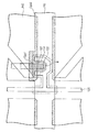
図9は本発明によるゲート/ソース間キャパシターの移転を説明する平面図である。
図9に示すように、一般的なゲート/ソース間キャパシタンスCgs1はチャンネル層上でゲート配線とドレイン配線がオーバーレイされる面積によって画定される。本発明による追加的なゲート/ソース間キャパシタンスCgs2はゲート配線110とピクセル電極142がオーバーレイされる面積によって画定される。
This will be described in more detail with reference to FIG.
FIG. 9 is a plan view illustrating transfer of a gate / source capacitor according to the present invention.
As shown in FIG. 9, the general gate / source capacitance Cgs1 is defined by the area where the gate wiring and the drain wiring are overlaid on the channel layer. The additional gate / source capacitance Cgs2 according to the present invention is defined by the area over which the
このように、追加的なゲート/ソース間キャパシタンスの面積をメインピクセルからサブピクセルに移転させることで、メインピクセルのキックバック電圧を顕著に減少させる。即ち、一般的なゲート/ソース間キャパシタンスCgs1の面積と追加的なゲート/ソース間キャパシタンスCgs2の面積比は略60:40である。
キックバック電圧Vkは下記する数式1によって画定される。
In this manner, the area of the additional gate / source capacitance is transferred from the main pixel to the sub-pixel, thereby significantly reducing the kickback voltage of the main pixel. That is, the area ratio of the general gate / source capacitance Cgs1 to the additional gate / source capacitance Cgs2 is approximately 60:40.
The kickback voltage Vk is defined by
Vk={Cgs over{Cgs+Cst+Clc}}cdot(Von−Voff )・・・(数式1)
ここで、Cgsはゲート/ソース間キャパシタンスであり、Cstはストレージキャパシタンスであり、Clcは液晶キャパシタンスであり、Vonはゲートオン電圧であり、Voffはゲートオフ電圧である。
Vk = {Cgs over {Cgs + Cst + Clc}} cdot (Von−Voff) (Equation 1)
Here, Cgs is a gate / source capacitance, Cst is a storage capacitance, Clc is a liquid crystal capacitance, Von is a gate-on voltage, and Voff is a gate-off voltage.
メインピクセルのキックバック電圧が減少されるとフリッカー現象のようなピクセルのRMS原因による画質不良が減少されるか除去される。
また、本発明によるPVAモードの液晶表示装置は低階調残象を改善する効果がある。それは、サブピクセルのガンマ曲線が中間諧調までブラックを保持するからである。
(実施例2)
図10は本発明の第2実施例による液晶表示パネルを説明する平面図である。
When the kickback voltage of the main pixel is reduced, image quality defects due to the RMS of the pixel such as flicker phenomenon are reduced or eliminated.
Further, the PVA mode liquid crystal display device according to the present invention has an effect of improving the low gradation residual image. This is because the gamma curve of the sub-pixel keeps black until the middle tone.
(Example 2)
FIG. 10 is a plan view illustrating a liquid crystal display panel according to a second embodiment of the present invention.
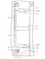
図11は図10に示されたアレイ基板200の平面図である。特に、スイッチング素子TFTから離れた位置に配置されるドレイン配線に形成されたコンタクトホールを有するアレイ基板を示す。
図2、図10及び図11に示すように、本発明の第2実施例によるアレイ基板200は基板上に図横方向に延設されるゲート配線210、ゲート配線210から延長されたゲート電極212、ゲート配線210から離間して設けられ単位ピクセル領域内でゲートライン210に平行に形成された第1及び第2下部ストレージパターンSTL、STL2及び単位ピクセル領域を横切る方向に設けられ単位ピクセルを2分割する第1カップリングパターンCPLを含む。
FIG. 11 is a plan view of the
As shown in FIGS. 2, 10 and 11, the
アレイ基板200は、窒化珪素SiNxなどの材質からなり、ゲート配線210及びゲート電極212をカバーするゲート絶縁層(図示せず)、及びゲート電極212をカバーするアクティブ層214を含む。アクティブ層214はa−Siのような半導体層、及び半導体層上に形成されたn+a−Siのような不純物層を含む。
アレイ基板200は図縦方向に延設されたソース配線220、ソース配線220から延長されたソース電極222、及びソース電極222と一定間隔離間して設けられるドレイン電極223を含む。ここで、ゲート電極212、半導体層214、半導体不純物層215、ソース電極222及びドレイン電極223は薄膜トランジスタTFTを画定する。
The
The
アレイ基板200は、ドレイン電極223から延長された第1上部ストレージパターン224、単位ピクセル領域の図右側に形成されドレイン電極223から延長された第1延長パターン225、第1延長パターン225に接続された第2カップリングパターン226、単位ピクセル領域の図右側に形成され第1延長パターン225に接続された第2延長パターン227及び第2延長パターン227に接続された第2上部ストレージパターン228を含む。
The
アレイ基板200は薄膜トランジスタTFTを覆いながらドレイン電極226の一部を露出するように順に積層されたパッシベーション層230と有機絶縁層(図示せず)を含む。パッシベーション層230と有機絶縁層は、ソース電極222とドレイン電極223との間のチャンネル層214をカバーして保護する役割及び薄膜トランジスタTFTとピクセル電極部240を絶縁する役割を実施する。チャンネル層214は半導体層214と半導体層214上に形成された半導体不純物層215を含む。
The
有機絶縁層の高さ調節を通じて液晶層200の厚さ(液晶層のセルギャップ)を調節することもできる。他の実施例においては、パッシベーション層230を省略することもできる。
アレイ基板200は、コンタクトホールCNTST1を通じて下部の第2カップリングパターン224と接続され開口されたパターン形状を有するピクセル電極部を含む。
Through adjustment of the height of the organic insulating layer, the thickness of the liquid crystal layer 200 (cell gap of the liquid crystal layer) can be adjusted. In other embodiments, the passivation layer 230 may be omitted.
The
具体的に、ピクセル電極部は、単位ピクセル領域の下側と上側にそれぞれ形成され単位ピクセル領域の図右側において、第1円超パターン225により電気的に接続されたメイン電極244及びサブ電極242を含む。メイン電極244は、図右側方向に向かうウェッジ形状を画定し、サブ電極242はメイン電極244が未形成された領域に形成される。
Specifically, the pixel electrode unit includes a
示された実施例において、メイン電極244には単位ピクセル領域において図横方向の軸を中心として対称な2つのY字形状の開口パターンが形成される。対称なY字形状の2つの分岐部(ゲート配線と平行でない部分)は90°の角度を有する。この開口パターンによって形成されたサブ電極242の幅は均一であることが望ましい。
サブ電極242の下側には、Y字形状の分岐部の一方と平行な2つの開口パターンが形成され、サブ電極242の上側にはY字形状の分岐部の他方と平行な2つの開口パターンが形成される。サブ電極242の上側に形成された2つの開口パターンはサブ電極242の下側に形成された2つの開口パターンと、図横方向の軸を基準として対称に形成される。
In the illustrated embodiment, the
Two opening patterns parallel to one of the Y-shaped branch portions are formed below the sub-electrode 242, and two opening patterns parallel to the other of the Y-shaped branch portions are formed above the sub-electrode 242. Is formed. The two opening patterns formed on the upper side of the
メイン及びサブ電極244、242に複数の開口パターンを形成することは、この後カラーフィルター基板との結合により収容される液晶層のドメインを複数個に分割するためである。
メイン電極244及びサブ電極242は、透明な導電性物質で形成することができる。このような透明な導電性物質の例としてはインジウム錫酸化物ITO、インジウム亜鉛酸化物IZO、亜鉛酸化物ZOなどを挙げることができる。
The reason why the plurality of opening patterns are formed in the main and
The
以上説明した本発明の第1実施例によると、ゲート配線とピクセル電極がオーバーレイされ発生する追加的なゲート/ソース間キャパシター(Cgs)面積をメインピクセルからサブピクセルに移行することで、メインピクセルのキックバック電圧を減少させ画質不良を改善することができる。
以上、説明した本発明の第2実施例によると、有機膜コンタクトホールの個数を2つに減少することで、工程及び有機膜材料の不良に対する信頼性を確保することができる。
According to the first embodiment of the present invention described above, an additional gate / source capacitor (Cgs) area generated by overlaying the gate wiring and the pixel electrode is shifted from the main pixel to the sub-pixel. It is possible to reduce the kickback voltage and improve image quality defects.
As described above, according to the second embodiment of the present invention described above, by reducing the number of organic film contact holes to two, it is possible to ensure reliability against defects in the process and the organic film material.
一般的なスーパーPVA構造におけるコンタクトホールは、ゲート配線とソース配線間のオーバーレイ部分に1ポイント、下部基板の共通電極層とソース配線間のオーバーレイ部分に2ポイント形成されるが、本発明の第2実施例においては、ゲート配線とソース配線間のオーバーレイ部分に1ポイント、下部基板の共通電極層とソース配線間のオーバーレイ部分に1ポイント形成するだけであり、ゲート/ソース間のショートポイントを減少することができる。ゲート/ソース間ショートポイント不良は三層膜MoAlMo上に有機膜を覆う工程でメイン不良中の1つである。 A contact hole in a general super PVA structure is formed at one point in the overlay portion between the gate wiring and the source wiring and at two points in the overlay portion between the common electrode layer of the lower substrate and the source wiring. In the embodiment, only one point is formed in the overlay portion between the gate wiring and the source wiring and only one point is formed in the overlay portion between the common electrode layer and the source wiring of the lower substrate, thereby reducing the short point between the gate and the source. be able to. The gate / source short point defect is one of the main defects in the process of covering the organic film on the three-layer film MoAlMo.
一般的なスーパーPVA構造では、サブピクセルを2つ形成する場合にはピクセル欠陥による検査が不利であったが、本発明の第2実施例によると、サブピクセルを1つにすることで、ピクセル結合検査に有利にし、アレイ検査の所要時間を減少することができる。
(実施例3)
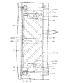
図12は本発明の第3実施例による液晶表示パネルを説明する平面図である。図13は図12に示されたアレイ基板300の平面図である。特に、スイッチング素子TFTに近接してストレージ配線と遠接するストレージ配線それぞれにコンタクトホールを形成し、中央部位のストレージ配線の幅を増加させアレイ基板を示す。
In the general super PVA structure, when two subpixels are formed, the inspection by the pixel defect is disadvantageous. However, according to the second embodiment of the present invention, the number of subpixels is reduced to one pixel. This is advantageous for bond inspection, and the time required for array inspection can be reduced.
(Example 3)
FIG. 12 is a plan view illustrating a liquid crystal display panel according to a third embodiment of the present invention. FIG. 13 is a plan view of the
図12及び図13に示すように、本発明の第3実施例によるアレイ基板300は基板上に図横方向に延設されたゲート配線310、ゲート配線310から延長されたゲート電極312、ゲート配線310から離間され単位ピクセル領域内でゲートライン310に平行に形成された第1及び第2下部ストレージパターンSTL1、STL2、及び単位ピクセル領域を横切るように形成され単位ピクセルを2分割する第1カップリングパターンCPLを含む。
As shown in FIGS. 12 and 13, an
アレイ基板300は、窒化珪素SiNxなどの材質からなり、ゲート配線310及びゲート電極312をカバーするゲート絶縁層(図示せず)及びゲート電極312をカバーするアクティブ層314を含む。アクティブ層314はa−Siのような半導体層及び半導体層上に形成されたn+a−Siのような半導体不純物層を含む。
アレイ基板300は、図縦方向に延設されたソース配線320、ソース配線320から延長されたソース電極322及びソース電極322と一定間隔で離間して設けられるドレイン電極323を含む。ここで、ゲート電極312、半導体層314、半導体不純物層315、ソース電極322及びドレイン電極323は薄膜トランジスタTFTを画定する。
The
The
アレイ基板300は、ドレイン電極323から延長され第1下部ストレージパターンSTL1を露出させる第1上部ストレージパターン324、単位ピクセル領域の図左側に形成され第1上部ストレージパターン324から延長された第1延長パターン325、第1延長パターン325に接続された第2カップリングパターン326、単位ピクセル領域の図左側に形成され第1延長パターン325に接続された第2延長パターン327及び第2延長パターン327に接続され第2下部ストレージパターンSTL2を露出させる第2上部ストレージパターン328を含む。
The
アレイ基板300は薄膜トランジスタTFTを覆いながらドレイン電極326の一部を露出するように順に積層されたパッシベーション層(図示せず)と、有機絶縁層(図示せず)を含む。パッシベーション層と有機絶縁層は、ソース電極322とドレイン電極323との間のチャンネル層314をカバーして保護する役割及び薄膜トランジスタTFTとピクセル電極部340を絶縁する役割を果たす。チャンネル層314は半導体層と半導体層上に形成された半導体不純物層を含む。
The
アレイ基板300は、コンタクトホールCNTCPを通じて下部の第2カップリングパターン326と接続され開口された開口パターン形状を有するピクセル電極部を含む。
具体的に、ピクセル電極部は第2カップリングパターン326とコンタクトするメイン電極344、第1下部ストレージパターンSTL1とコンタクトする第1サブ電極342及び第1サブ電極342と分離され第2下部ストレージパターンSTL2とコンタクトする第2サブ電極346を含む。
The
Specifically, the pixel electrode part is separated from the
示された実施例において、メイン電極344には単位ピクセル領域において図横方向の軸を中心として対称な2つのY字形状の開口パターンが形成される。対称なY字形状の2つの分岐部は90°の角度を有する。第1サブ電極342にはY字形状の分岐部のうち一方と平行な2つの開口パターンが形成される。第2サブ電極346にはY字形状の分岐部の他方と平行であり第1サブ電極342に形成された開口パターンと図横方向の軸を基準として対称な2つの開口パターンが形成される。メイン電極344、第1及び第2サブ電極342、346に複数の開口パターンを形成するのは、この後カラーフィルター基板との結合により収容される液晶層のドメインを複数個に分割するためである。
In the illustrated embodiment, the
メイン電極344、第1及び第2サブ電極324、246は透明な導電性物質で形成することができる。このような透明な導電性物質の例としてはインジウム錫酸化物ITO、インジウム亜鉛酸化物IZO、亜鉛酸化物ZOなどを挙げることができる。
平面上で観察するとき、メイン電極344、第1及び第2サブ電極342、346それぞれによって互いに異なる複数のドメインが形成される。従って、前記したアレイ基板やカラーフィルター基板に形成され液晶を配向する配向膜の表面を一定の方向にラビングする工程の省略も可能で、配向膜を形成しなくてもよい。
The
When observed on a plane, a plurality of domains different from each other are formed by the
以上、説明した本発明の第3実施例によると、ゲート配線とピクセル電極とがオーバーレイされ発生する追加的なゲート/ソース間キャパシター(Cgs)面積をメインピクセルからサブピクセルに移転させることで、メインピクセルのキックバック電圧を減少させ画質不良を改善することができる。
(実施例4)
図14は本発明の第4実施例による液晶表示パネルを説明する平面図である。図15は図14に示されたアレイ基板400の平面図である。特に、スイッチング素子TFTに近接するドレイン配線、遠接するドレイン配線に形成されたコンタクトホール、及び中央部位のストレージ配線の幅を増加させたアレイ基板を示す。
As described above, according to the third embodiment of the present invention, an additional gate / source capacitor (Cgs) area generated by overlaying the gate wiring and the pixel electrode is transferred from the main pixel to the sub-pixel. Pixel kickback voltage can be reduced and image quality defects can be improved.
Example 4
FIG. 14 is a plan view illustrating a liquid crystal display panel according to a fourth embodiment of the present invention. FIG. 15 is a plan view of the
図14及び図15に示すように、本発明の第4実施例によるアレイ基板400は基板上に図横方向に延設されたゲート配線410、ゲート配線410から延長されたゲート電極412、ゲート配線410から離間して設けられ単位ピクセル領域内にゲートライン410と平行に形成された第1及び第2下部ストレージパターンSTL1、STL2、及び単位ピクセル領域を横切って設けられ単位ピクセル領域を2分割する第1カップリングパターンCPLを含む。
As shown in FIGS. 14 and 15, an
アレイ基板400は窒化珪素SiNxなどの材質からなりゲート配線410及びゲート電極412をカバーするゲート絶縁層(図示せず)、及びゲート電極412をカバーするアクティブ層414を含む。アクティブ層414はa−Siのような半導体層、及び半導体層上に形成されたn+a−Siのような半導体不純物層を含む。
アレイ基板400は、図縦方向に延設されたソース配線420、ソース配線420から延長されたソース電極422及びソース電極422と一定間隔離間して設けられたドレイン電極423を含む。ここで、ゲート電極412、半導体層414、半導体不純物層415、ソース電極422及びドレイン電極423は薄膜トランジスタTFTを画定する。
The
The
アレイ基板400は第1上部ストレージパターン424、第1延長パターン425、第2カップリングパターン426、第2延長パターン427及び第2上部ストレージパターン428を含む。
具体的に、第1上部ストレージパターン424は、ドレイン電極423から延長され第1下部ストレージパターンSTL1上に形成される。第1延長パターン425は単位ピクセ領域を図縦に分割するようにセンターに形成され、第1上部ストレージパターン424から延長される。第2カップリングパターン426は、第1延長パターン425に接続され第1カップリングパターンCPLをカバーする。第2延長パターン427は単位ピクセル領域を図縦に分割するようにセンターに形成され、第1延長パターン425に接続される。第2上部ストレージパターン428は第2延長パターン427に接続され第2下部ストレージパターンSTL2上に形成される。
The
Specifically, the first
アレイ基板400は薄膜トランジスタTFTを覆いながらドレイン電極426の一部を露出するように、順に積層されたパッシベーション層(図示せず)と有機絶縁層(図示せず)を含む。パッシベーション層と有機絶縁層はソース電極422とドレイン電極423との間のチャンネル層414をカバーして保護する役割及び薄膜トランジスタTFTとピクセル電極部440とを絶縁する役割を果たす。チャンネル層414は、半導体層と、半導体層上に形成された半導体不純物層を含む。
The
アレイ基板400はコンタクトホール(CNTCP)を通じて下部の第2カップリングパターン426と接続され開口された開口パターン形状を有するピクセル電極部を含む。
具体的に、ピクセル電極部は第2カップリングパターン426とコンタクトするメイン電極444、第1下部ストレージパターンSTL1とコンタクトする第1サブ電極442、第1サブ電極442と分離され第2下部ストレージパターンSTL2とコンタクトする第2サブ電極446を含む。
The
Specifically, the pixel electrode part is separated from the
示された実施例において、メイン電極444には単位ピクセル領域において横方向の軸を中心として対称な2つのY字形状の開口パターンが形成される。対称なY字形状の2つの分岐部は90°の角度を有する。
第1サブ電極442にはY字形状の分岐部の一方と平行な2つの開口パターンが形成される。
In the illustrated embodiment, the
In the
第2サブ電極446にはY字形状の分岐部の他方と平行であり第1サブ電極442に形成された開口パターンと図横方向の軸を基準として対称な2つの開口パターンが形成される。メイン電極444、第1及び第2サブ電極442、446に複数の開口パターンを形成するのは、この後カラーフィルター基板との結合により収容される液晶層のドメインを複数個に分割するためである。
The
メイン電極444、第1及び第2サブ電極442、446は透明な導電性物質で形成することができる。このような透明な導電性物質の例としてはインジウム錫酸化物ITO、インジウム亜鉛酸化物IZO、亜鉛酸化物ZOなどを挙げることができる。
平面上で観察するとき、メイン電極444、第1及び第2サブ電極442、446それぞれによって互いに異なる複数のドメインが形成される。従って、前記したアレイ基板やカラーフィルター基板に形成され液晶を配向する配向膜の表面を一定の方向にラビングする工程の省略も可能で、配向膜を省略することもできる。
The
When observed on a plane, a plurality of domains different from each other are formed by the
以上で、説明した本発明の第4実施例によると、ゲート配線とピクセル電極がオーバーレイされ発生する追加的なゲート/ソース間キャパシター(Cgs)面積をメインピクセルからサブピクセルに移行することで、メインピクセルのキックバック電圧を減少させ画質不良を改善することができる。
(実施例5)
図16は本発明の第5実施例による液晶表示パネルを説明する平面図である。図17は図16に示されたアレイ基板500の平面図である。特に、スイッチング素子TFTに近接してドレイン配線にコンタクトホールを形成し、中央部位のストレージ配線の幅を増加させたアレイ基板を示す。
As described above, according to the fourth embodiment of the present invention, an additional gate / source capacitor (Cgs) area generated by overlaying the gate wiring and the pixel electrode is shifted from the main pixel to the sub-pixel. Pixel kickback voltage can be reduced and image quality defects can be improved.
(Example 5)
FIG. 16 is a plan view for explaining a liquid crystal display panel according to a fifth embodiment of the present invention. FIG. 17 is a plan view of the
図16及び図17に示すように、本発明の第5実施例によるアレイ基板500は基板上に図横方向に延設されたゲート配線510、ゲート配線510から延長されたゲート電極512、ゲート配線510から離間して設けられ単位ピクセル領域内でゲートライン510と平行に形成された第1下部ストレージパターンSTL及び単位ピクセル領域を横切って単位ピクセルを2分割する第1カップリングパターンCPLを含む。
As shown in FIGS. 16 and 17, an
アレイ基板500は、窒化珪素SiNxなどの材質からなり、ゲート配線510及びゲート電極512をカバーするゲート絶縁層(図示せず)及びゲート電極512をカバーするアクティブ層514を含む。アクティブ層514はa−Siのような半導体層及び半導体層上に形成されたn+a−Siのような半導体不純物層を含む。
アレイ基板500は縦方向に伸長されたソース配線520、ソース薄膜520から延長されたソース電極522及びソース電極522と一定間隔離間して形成されるドレイン電極523を含む。ここで、ゲート電極512、半導体層514、半導体不純物層515、ソース電極522及びドレイン電極523は薄膜トランジスタTFTを画定する。
The
The
アレイ基板500は、ドレイン電極523から延長され第1下部ストレージパターン(STL)上に形成された第1上部ストレージパターン524、単位ピクセル領域の図左側に形成され第1上部ストレージパターン524から延長された第1延長パターン525及び第1延長パターン535に接続され第1カップリングパターンCPLをカバーする第2カップリングパターン526を含む。
The
アレイ基板500は、薄膜トランジスタTFTを覆うとともにドレイン電極526の一部を露出するように順に積層されたパッシベーション層(図示せず)と有機絶縁層(図示せず)を含む。パッシベーション層と有機絶縁層はソース電極522とドレイン電極523との間のチャンネル層514をカバーし保護する役割及び薄膜トランジスタTFTとピクセル電極部540を絶縁する役割を果たす。チャンネル層514は半導体層と半導体層上に形成された半導体不純物層を含む。
The
アレイ基板500は、コンタクトホールCNTCPを通じて下部の第2カップリングパターン526と接続され開口された開口パターン形状を有するピクセル電極部を含む。
具体的に、ピクセル電極部は、単位ピクセル領域の中央部を介して第2カップリングパターン526を経由して電気的に接続されたメイン電極544およびサブ電極542を含む。メイン電極544は図右側方向に尖端を有するくさび形状であり、サブ電極542はメイン電極542が形成されていない領域に形成される。
The
Specifically, the pixel electrode unit includes a
示された実施例において、メイン電極544には単位ピクセル領域において図横方向の軸を中心として対称な2つのY字形状の開口パターンが形成される。対称なY字形状の2つの分岐部は90°の角度を有する。
サブ電極542のうちメイン電極544の下側に位置する領域には、メイン電極544に設けられたY字形状の開口パターンのうち一方の分岐部と平行な2つの開口パターンが形成さる。また、サブ電極542のうちメイン電極544の上側に位置する領域には、メイン電極544に設けられたY字形状の開口パターンのうちの他方の分岐部と平行な2つの開口パターンが形成される。メイン電極544の上側に位置する領域に形成された2つの開口パターンと、メイン電極544の下側に位置する領域に形成された2つの開口パターンとは、横方向の軸を基準として対称に形成される。
In the illustrated embodiment, the
In the region of the
メイン及びサブ電極544、542に複数の開口パターンを形成するのは、この後カラーフィルター基板との結合により収容される液晶層のドメインを複数個に分割するためである。
メイン電極544及びサブ電極542は透明な導電性物質で形成される。このような透明な導電性物質の例としてはインジウム錫酸化物ITO、インジウム亜鉛酸化物IZO、亜鉛酸化物ZOなどを挙げることができる。
The reason why the plurality of opening patterns are formed in the main and
The
平面上で観察するとき、メイン電極544及びサブ電極542それぞれによって互いに異なる複数のドメインが形成される。従って、前記したアレイ基板やカラーフィルター基板に形成され液晶を配向する配向膜の表面を一定の方向にラビングする工程の省略も可能であり、配向膜を省略することも可能である。
以上、説明した本発明の第5実施例によると、ゲート配線とピクセル電極とのオーバーレイにより発生する追加的なゲート/ソース間キャパシター(Cgs)面積をメインピクセルからサブピクセルに移転させることで、メインピクセルのキックバック電圧を減少させ画質不良を改善することができる。
When observed on a plane, a plurality of domains different from each other are formed by the
As described above, according to the fifth embodiment of the present invention, the additional gate / source capacitor (Cgs) area generated by the overlay of the gate wiring and the pixel electrode is transferred from the main pixel to the sub-pixel. Pixel kickback voltage can be reduced and image quality defects can be improved.
以上、説明した本発明の第5実施例によると、有機膜コンタクトホールの個数を2つに減少することで、工程及び有機膜材料の不良に対する信頼性を確保することができる。
一般的なスーパーPVA構造におけるコンタクトホールは、ゲート配線とソース配線と間のオーバーレイ部分に1ポイント、下部基板の共通電極層とソース配線と間のオーバーレイ部分に2ポイントに形成される反面、本発明の第5実施例におけるコンタクトホールは、ゲート配線とソース配線と間のオーバーレイ部分に1ポイント、下部基板の共通電極層とソース配線と間のオーバーレイ部分に1ポイント形成するだけであり、ゲート/ソース間ショートポイントを減少することができる。ゲート/ソース間ショートポイント不良は、三層膜配線MoAlMo上に有機膜を覆う工程でメイン不良中の1つである。
As described above, according to the fifth embodiment of the present invention described above, by reducing the number of organic film contact holes to two, it is possible to ensure reliability against defects in the process and the organic film material.
In the general super PVA structure, the contact hole is formed at one point in the overlay portion between the gate wiring and the source wiring and at two points in the overlay portion between the common electrode layer of the lower substrate and the source wiring. In the fifth embodiment, the contact hole is formed only at one point in the overlay portion between the gate wiring and the source wiring and at one point in the overlay portion between the common electrode layer of the lower substrate and the source wiring. Between short points can be reduced. The gate / source short point defect is one of the main defects in the process of covering the organic film on the three-layer film wiring MoAlMo.
一般的なスーパーPVA構造ではサブピクセルが2つに形成され、ピクセル欠陥の検査において不利であったが、本発明の第5実施例によると、サブピクセルを1つに形成することで、ピクセル欠陥検査に有利で、アレイ検査の所要時間を減少させることができる。
(実施例6)
図18は本発明の第6実施例による液晶表示パネルを説明する平面図である。図19は図18に示されたアレイ基板600の平面図である。特に、図1と比較するときスイッチング素子に近接する位置に配置されるドレイン配線とスイッチング素子から遠い位置に配置されたドレイン配線それぞれにコンタクトホールを形成し、スイッチング素子に近接する位置のドレイン配線と素一Tin具素子から遠い位置のドレイン配線とを接続する配線をピクセルの中央部位に移動したアレイ基板を示す。
In the general super PVA structure, the subpixels are formed in two, which is disadvantageous in the inspection of pixel defects. However, according to the fifth embodiment of the present invention, pixel defects are formed by forming the subpixels in one. This is advantageous for inspection, and the time required for array inspection can be reduced.
(Example 6)
FIG. 18 is a plan view illustrating a liquid crystal display panel according to a sixth embodiment of the present invention. FIG. 19 is a plan view of the
図18及び図19に示すように、本発明の第6実施例によるアレイ基板600は基板上に図横方向に延設されたゲート配線610、ゲート配線610から延長されたゲート電極612、ゲート配線610から離間して設けられ単位ピクセル領域内でゲートライン610と平行するように形成された第1及び第2下部ストレージパターンSTL1、STL2及び単位ピクセル領域を横切って設けられ単位ピクセルを2分割する第1カップリングパターンCPLを含む。
As shown in FIGS. 18 and 19, an
アレイ基板600は、窒化珪素(SiNx)などの材質からなり、ゲート配線610及びゲート電極612をカバーするゲート絶縁層(図示せず)及びゲート電極612をカバーするアクティブ層614を含む。アクティブ層614はa−Siのような半導体層及び半導体層上に形成されたn+a−Siのような半導体不純物層を含む。
アレイ基板600は、図縦方向に延設されたソース配線620、ソース配線620で延長されたソース電極622及びソース電極622と一定間隔離間して設けられるドレイン電極623を含む。ここで、ゲート電極612、半導体層614、半導体不純物層615、ソース電極622及びドレイン電極623は薄膜トランジスタTFTを画定する。
The
The
アレイ基板600は、第1上部ストレージパターン624、第1延長パターン625、第2カップリングパターン626、第2延長パターン627及び第2上部ストレージパターン628を含む。
具体的に、第1上部ストレージパターン624は、ドレイン電極623から延長され第1下部ストレージパターンSTL1上に形成される。第1延長パターン625は単位ピクセル領域を上下に分割するようにセンターに形成され第1上部ストレージパターン624から延長される。第2カップリングパターン626は、第1延長パターン625に接続され第1カップリングパターンCPLをカバーする。第2延長パターン627は単位ピクセル領域を上下に分割するようにセンターに形成され第1延長パターン625に接続される。第2上部ストレージパターン628は、第2延長パターン627に接続され第2下部ストレージパターンSTL2上に形成される。
The
Specifically, the first
アレイ基板600は、薄膜トランジスタTFTを覆うとともにドレイン電極626の一部を露出するように順に積層されたパッシベーション層(図示せず)と有機絶縁層(図示せず)を含む。パッシベーション層と有機絶縁層はソース電極622とドレイン電極623との間のチャンネル層614をカバーして保護する役割及び薄膜トランジスタTFTとピクセル電極部640を絶縁する役割を果たす。チャンネル層614は半導体層と半導体層上に形成された半導体不純物層を含む。
The
アレイ基板600は、所定形状の開口パターンを有し、コンタクトホールCNTCPを通じて下部の第2カップリングパターン626と接続されるピクセル電極部を含む。
具体的に、ピクセル電極部は第2カップリングパターン626とコンタクトするメイン電極644、第1下部ストレージパターンSTL1とコンタクトする第1サブ電極642及び第1サブ電極642と分離され第2下部ストレージパターンSTL2とコンタクトする第2サブ電極646を含む。
The
Specifically, the pixel electrode part is separated from the
示された実施例において、メイン電極644には単位ピクセル領域において横方向の軸を中心として対称な2つのY字形状の開口パターンが形成される。この対称なY字形状の2つの分岐部は90°の角度を有する。
第1サブ電極642にはメイン電極644に形成されたY字形状の開口パターンのうち一方の分岐部と平行な2つの開口パターンが形成される。
In the illustrated embodiment, the
The
第2サブ電極646にはメイン電極644に形成されたY字形状の開口パターンのうち他方の分岐部と平行であり第1サブ電極642に形成された開口パターンと横方向の軸を基準として対称な2つの開口パターンが形成される。メイン電極644、第1及び第2サブ電極642、446に複数の開口パターンを形成するのは、この後カラーフィルター基板との結合により収容される液晶層のドメインを複数個に分割するためである。
The
メイン電極644、第1及び第2サブ電極642、446は透明な導電性物質から形成される。このような透明な導電性物質の例としてはインジウム錫酸化物ITO,インジウム亜鉛酸化物IZO、亜鉛酸化物ZOなどを挙げることができる。
平面上で観察するとき、メイン電極644、第1及び第2サブ電極642、446はそれぞれによって互いに異なる複数のドメインが形成される。従って、前記したアレイ基板やカラーフィルター基板に形成され液晶を配向する配向膜の表面を一定の方向にラビングする工程の省略も可能で、配向膜を省略することも可能である。
The
When observed on a plane, the
以上、本発明の第6実施例によると、ゲート配線とピクセル電極がオーバーレイすることにより発生する追加的なゲート/ソース間キャパシター(Cgs)面積をメインピクセルからサブピクセルに移行することで、メインピクセルのキックバック電圧を減少し画質不良を改善することができる。
以上、説明した本発明の第6実施例によると、ドレイン配線を単位ピクセルの中央に配置することで、ソース配線とドレイン配線と間に発生するショートを防止することができる。
As described above, according to the sixth embodiment of the present invention, the additional gate / source capacitor (Cgs) area generated by overlaying the gate wiring and the pixel electrode is shifted from the main pixel to the sub-pixel. Image quality can be improved by reducing the kickback voltage.
As described above, according to the sixth embodiment of the present invention, by arranging the drain wiring at the center of the unit pixel, it is possible to prevent a short circuit between the source wiring and the drain wiring.
(実施例7)
図20は本発明の第7実施例による液晶表示パネルを説明する平面図である。図21は図20に示されたアレイ基板700の平面図である。特に、図17と比較するときスイッチング素子TFTから離れた位置に配置されるドレイン配線にコンタクトホールを形成し、スイッチング素子TFTに近接する位置に配置されるドレイン配線とスイッチング素子TFTから離れた位置に配置されるドレイン配線を接続する配線をピクセルの中央部位に移動したアレイ基板を示す。
(Example 7)
FIG. 20 is a plan view illustrating a liquid crystal display panel according to a seventh embodiment of the present invention. FIG. 21 is a plan view of the
図20及び図21に示すように、本発明の第7実施例によるアレイ基板700は基板上に図横方向に延設されたゲート配線710、ゲート配線710から延長されたゲート電極712、ゲート配線710から離間して形成され単位ピクセル領域内でゲートライン710と平行に形成された第1及び第2下部ストレージパターンSTL1、STL2及び単位ピクセル領域を横切って単位ピクセルを2分割する第1カップリングパターンCPLを含む。
As shown in FIGS. 20 and 21, an
アレイ基板700は窒化珪素SiNxなどの材質からなり、ゲート配線710及びゲート電極712をカバーするゲート絶縁層(図示せず)と、ゲート電極712をカバーするアクティブ層714を含む。アクティブ層714はa−Siのような半導体層と、半導体層上に形成されたn+a−Siのような半導体不純物層を含む。
アレイ基板700は図縦方向に延設されたソース配線720、ソース配線720から延長されたソース電極722及びソース電極722と一定間隔離間して形成されるドレイン電極723を含む。ここで、ゲート電極712、半導体層714、半導体不純物層715、ソース電極722及びドレイン電極723は薄膜トランジスタTFTを画定する。
The
The
アレイ基板700は、第1上部ストレージパターン724、第1延長パターン725、第2カップリングパターン726、第2延長パターン727及び第2上部ストレージパターン728を含む。
具体的に、第1上部ストレージパターン724は、ドレイン電極723から延長され第1下部ストレージパターンSTL1上に形成される。第1延長パターン725は単位ピクセル領域を上下に分割するようにセンターに形成され第1上部ストレージパターン724から延長される。第2カップリングパターン726は、第1延長パターン725に接続され第1カップリングパターンCPLをカバーする。第2延長パターン727は、単位ピクセル領域を上下に分割するようにセンターに形成され第1延長パターン725に接続される。第2上部ストレージパターン728は第2延長パターン727に接続され第2下部ストレージパターンSTL2上に形成される。
The
Specifically, the first
アレイ基板700は薄膜トランジスタTFTを覆うとともにドレイン電極726の一部を露出するように順に積層されたパッシベーション層(図示せず)と有機絶縁層(図示せず)を含む。パッシベーション層と有機絶縁層はソース電極722とドレイン電極723との間のチャンネル層714をカバーして保護する役割及び薄膜トランジスタTFTとピクセル電極部740とを絶縁する役割を果たす。チャンネル層714は半導体層と半導体層上に形成された半導体不純物層を含む。
The
アレイ基板700は所定形状で形成される開口パターンを有し、コンタクトホールCNTCPを通じて下部の第2カップリングパターン726と接続されたピクセル電極部を含む。
具体的に、ピクセル電極部は、単位ピクセル領域の中央領域に位置して形成されるサブ電極744と、サブ電極744の下側と上側にそれぞれ形成され単位ピクセル領域の図右側を通じて接続されたメイン電極742を含む。サブ電極744は右側方向に向かって尖端を有するくさび形状で構成され、メイン電極742はサブ電極744が形成されていない領域に形成される。
The
Specifically, the pixel electrode unit includes a sub-electrode 744 formed in the central region of the unit pixel region, and a main electrode connected to the lower side and the upper side of the sub-electrode 744 through the right side of the unit pixel region. An
示された実施例において、サブ電極744には単位ピクセル領域において横方向の軸として対称な2つのY字形状の開口パターンが形成される。開口パターンの対称なY字形状の2つの分岐部は90°の角度を有する。
メイン電極742のうちサブ電極744の下側に位置する領域には、サブ電極744に形成される開口パターンの一方の分岐部と平行な2つの開口パターンが形成され、メイン電極742のうちサブ電極744の上側に位置する領域には、サブ電極744に形成される開口パターンの他方の分岐部と平行な2つの開口パターンが形成される。メイン電極742の上側領域に形成された2つの開口パターンはメイン電極742の下側領域に形成された2つの開口パターンと、横方向の軸を基準として対称に形成される。
In the illustrated embodiment, the sub-electrode 744 is formed with two Y-shaped opening patterns that are symmetrical with respect to the horizontal axis in the unit pixel region. The two symmetrical Y-shaped branches of the opening pattern have an angle of 90 °.
In the region of the
メイン電極742及びサブ電極744に複数の開口パターンを形成するのは、この後カラーフィルターとの結合により収容される液晶層のドメインを複数個に分割するためである。
メイン電極742及びサブ電極744は透明な導電性物質で形成することができる。このような透明な導電性物質の例としてはインジウム錫酸化物ITO、インジウム亜鉛酸化物IZO、亜鉛酸化物ZOなどを挙げることができる。
The reason why the plurality of opening patterns are formed in the
The
本発明の第7実施例によると、ゲート配線とピクセル電極とがオーバーレイして発生する追加的なゲート/ソース間キャパシター(Cgs)面積をメインピクセルからサブピクセルに移行することで、メインピクセルキックバック電圧を減少させ画質不良を改善することができる。
以上、説明した本発明の第7実施例によると、有機膜コンタクトホールの個数を2つに減少させることで、工程及び有機膜材料の不良に対する信頼性を確保することができる。
According to the seventh embodiment of the present invention, an additional gate / source capacitor (Cgs) area generated by overlaying a gate line and a pixel electrode is shifted from a main pixel to a sub-pixel, thereby main pixel kickback. It is possible to reduce the voltage and improve image quality defects.
As described above, according to the seventh embodiment of the present invention described above, by reducing the number of organic film contact holes to two, it is possible to ensure reliability against defects in the process and the organic film material.
一般的なスーパーPVA構造におけるコンタクトホールは、ゲート配線とソース配線と間のオーバーレイ部分に1ポイント、下部基板の共通電極層とソース配線と間のオーバーレイ部分に2ポイントに形成される反面、本発明の第7実施例においてはゲート配線とソース配線と間のオーバーレイ部分に1ポイント、下部基板の共通電極層とソース配線と間のオーバーレイ部分に1ポイントだけ形成されるので、ゲート/ソース間ショートポイントを減少することができる。ゲート/ソース間ショートポイント不良は三層膜配線MoAlMo上に有機膜を覆う工程においてメイン不良中の1つである。 In the general super PVA structure, the contact hole is formed at one point in the overlay portion between the gate wiring and the source wiring and at two points in the overlay portion between the common electrode layer of the lower substrate and the source wiring. In the seventh embodiment, only one point is formed in the overlay portion between the gate wiring and the source wiring, and only one point is formed in the overlay portion between the common electrode layer of the lower substrate and the source wiring. Can be reduced. The gate / source short point failure is one of the main failures in the process of covering the organic film on the three-layer film wiring MoAlMo.
一般的なスーパーPVA構造では、サブピクセルが2つ形成されることによりピクセル欠陥の検査において不利であったが、本発明の第7実施例によると、サブピクセルを1つに形成することで、ピクセル欠陥検査に有利で、アレイ検査の所要時間を減少することができる。
以上、説明した本発明の第7実施例によると、ドレイン配線を単位ピクセルの中央に配置することで、ソース配線とドレイン配線と間に発生するショートを防止することができる。
In the general super PVA structure, the formation of two subpixels is disadvantageous in the inspection of the pixel defect. According to the seventh embodiment of the present invention, by forming the subpixels into one, This is advantageous for pixel defect inspection, and the time required for array inspection can be reduced.
As described above, according to the seventh embodiment of the present invention, by arranging the drain wiring at the center of the unit pixel, it is possible to prevent a short circuit between the source wiring and the drain wiring.
前述した本発明の第1乃至第7実施例においては、1つのスイッチング素子が単位ピクセル領域に形成された構造において、メインピクセルとサブピクセルの構成の変更が行われる場合を説明したが、下記の本発明の第8実施例のように2つのスイッチング素子が単位ピクセル領域に形成された構造にも適用することができる。
(実施例8)
図22は本発明の第8実施例による液晶表示パネルを説明する平面図である。図23は図22に示されたアレイ基板800の平面図である。特に、単位ピクセル領域に2つのスイッチング素子TFTを形成し、中央部位のストレージ配線と接続されたドレイン電極を有するスイッチング素子TFTが形成された領域をメインピクセルと画定し、端部位のストレージ配線と接続されたドレイン電極を有するスイッチング素子TFTが形成された領域をサブピクセルとして画定する。
In the first to seventh embodiments of the present invention described above, the case where the configuration of the main pixel and the sub pixel is changed in the structure in which one switching element is formed in the unit pixel region has been described. The present invention can also be applied to a structure in which two switching elements are formed in a unit pixel region as in the eighth embodiment of the present invention.
(Example 8)
FIG. 22 is a plan view illustrating a liquid crystal display panel according to an eighth embodiment of the present invention. FIG. 23 is a plan view of the
図22及び図23に示すように、本発明の第8実施例によるアレイ基板800は単位ピクセル領域で図横方向に延設された第1及び第2ゲート配線810M、810S、第1及び第2ゲート配線810M、810Sのそれぞれから延長された第1及び第2ゲート電極812M,812S、第1及び第2ゲート配線810M、810Sから離間して設けられ単位ピクセル領域内で第1ゲートライン810Mと垂直方向に形成された第1下部ストレージパターンSTL及び単位ピクセル領域を横切って単位ピクセルを2分割する第1カップリングパターンCPLを含む。第1カップリングパターンCPLは単位ピクセルの右側領域で第1下部ストレージパターンSTLと接続される。
As shown in FIGS. 22 and 23, the
アレイ基板800は、窒化珪素などの材質からなり第1及び第2ゲート配線810M、810S、第1及び第2ゲート電極812M、812Sをカバーするゲート絶縁層(図示せず)及び第1及び第2ゲート電極812M、812Sそれぞれをカバーする第1及び第2アクティブ層814M、814Sを含む。第1及び第2アクティブ層814M、814Sはa−Siのような半導体層と、半導体層上に形成されたn+a−Siのような半導体不純物層を含む。
The
アレイ基板800は、図縦方向に延設されたソース配線820、ソース配線820から延長された第1及び第2ソース電極822M、822S及び第1及び第2ソース電極822M、822Sとそれぞれ一定間隔で離間して設けられる第1及び第2ドレイン電極823M、823Sを含む。ここで、第1ゲート電極812M、第1アクティブ層814M、第1ソース電極822M及び第1ドレイン電極823Mはメイン薄膜トランジスタTFTを画定する。また、第2ゲート電極812S、第2アクティブ層814S、第2ソース電極822S及び第2ドレイン電極823Sはサブ薄膜トランジスタTFTを画定する。
The
アレイ基板800は、第2ドレイン電極823Sから延長され第1下部ストレージパターンSTL上に形成された上部ストレージパターン824S及び単位ピクセル領域の右側に形成され上部ストレージパターン824Sから延長された第1延長パターン825Sを含む。
アレイ基板800は第1ドレイン電極823Mから延長され第1カップリングパターンCPLをカバーする第2カップリングパターン826を含む。
The
The
アレイ基板800はメイン及びサブ薄膜トランジスタを覆うとともにストレージパターン824Sの一部と第2カップリングパターン826の一部を露出するように順に積層されたパッシベーション層(図示せず)と有機絶縁層(図示せず)を含む。
パッシベーション層と有機絶縁層は第1ソース電極822Mと第1ドレイン電極823Mとの間の第1チャンネル層814M及び第2ソース電極822Sと第2ドレイン電極823Sとの間の第2チャンネル層814Sをカバーして保護する役割と、メイン及びサブ薄膜トランジスタとピクセル電極部とを絶縁する役割を果たす。第1及び第2チャンネル層814M、814Sそれぞれは半導体層及び半導体層上に形成された半導体不純物層を含む。
The
The passivation layer and the organic insulating layer cover the
アレイ基板800は、コンタクトホールCNTCPを通じて下部の第2カップリングパターン826と電気的に接続され所定形状の開口パターンを有するメイン電極部844及びコンタクトホールCNTST1を通じて下部の上部ストレージパターン824Sと電気的に接続され所定形状の開口パターンを有するサブ電極部842を含む。
メイン電極部844は図右側方向に向かって尖端を有するくさび形状に形成され、サブ電極842はメイン電極844が形成されていない領域、即ち、単位ピクセル領域においてメイン電極844の下側及び上側に形成される。
The
The
メイン電極部844は、単位ピクセル領域において図横方向の軸を中心として対称であり互いに接続された3つのV字形状を構成しており、このような形状を構成するための開口パターンを含む。V字形状の領域のうち大きいサイズの領域と中間サイズの領域は図左側領域のエッジで接続され、中間サイズの領域と小さいサイズの領域は中央部で接続される。V字形状の内角は90°である。V字形状の領域の幅は均一であることが望ましい。
The
サブ電極842のうちメイン電極844の下側に位置する部分には、V字形状の領域の一方の領域と平行な2つの開口パターンが形成され、サブ電極842のうちメイン電極844の上側に位置する領域にはV字形状の領域のうち他方の領域と平行な2つの開口パターンが形成される。サブ電極842のうちメイン電極844の上側に位置する領域に形成された2つの開口パターンは、サブ電極842のうちメイン電極844の下側に位置する領域に形成された2つの開口パターンと図横方向の軸を基準として対称に形成される。
Two opening patterns parallel to one of the V-shaped regions are formed in a portion of the sub-electrode 842 positioned below the
メイン及びサブ電極844、842に複数の開口パターンを形成するのは、この後カラーフィルター基板との結合により収容される液晶層のドメインを複数個に分割するためである。
メイン電極844及びサブ電極842は透明な導電性物質で形成される。このような透明な導電性物質の例としてはインジウム錫酸化物ITO、インジウム亜鉛酸化物IZO、亜鉛酸化物ZOなどを挙げることができる。
The reason why the plurality of opening patterns are formed in the main and
The
平面上で観察するとき、メイン電極844及びサブ電極842それぞれによって互いに異なる複数のドメインが形成される。従って、前記したアレイ基板やカラーフィルター基板に形成され液晶を配向する配向膜の表面を一定の方向にラビングする工程の省略も可能で、配向膜を省略することも可能である。
以上、説明したように、本発明によると、PVA構造で、ゲート背面とピクセル電極が重畳されることによって発生する追加的なゲート/ソース間キャパシターの面積をメインピクセルからサブピクセルに移行することで、メインピクセルのキックバック電圧を減少しフリッカーのようにピクセルのRMS原因により発生される画質不良を改善することができる。
When observed on a plane, a plurality of domains different from each other are formed by the
As described above, according to the present invention, in the PVA structure, the area of the additional gate / source capacitor generated by overlapping the gate back surface and the pixel electrode is shifted from the main pixel to the subpixel. Therefore, the kickback voltage of the main pixel can be reduced to improve the image quality defect caused by the RMS of the pixel like flicker.
また、サブピクセルのガンマ曲線が中間階調までブラックを保持するのでPVAの低階調残像改善に効果がある。
また、有機膜コンタクトホールの個数を2つに減少することで、工程及び有機膜材料の不良に対する信頼性を確保することができる。
また、一般的なスーパーPVA構造では、コンタクトホールをゲート配線とソース配線と間のオーバーレイ部分に1ポイント、下部基板の共通電極層とソース配線と間のオーバーレイ部分に2ポイントに形成しているが、本発明においてはゲート配線とソース配線と間のオーバーレイ部分に1ポイント、下部基板の共通電極層とソース配線間のオーバーレイ部分に1ポイント形成するだけであり、ゲート/ソース間ショートポイントを減少することができる。
Further, since the gamma curve of the subpixel holds black up to the intermediate gradation, it is effective in improving the low gradation afterimage of PVA.
Further, by reducing the number of organic film contact holes to two, it is possible to ensure reliability against defects in the process and the organic film material.
In the general super PVA structure, the contact hole is formed at one point in the overlay portion between the gate wiring and the source wiring, and at two points in the overlay portion between the common electrode layer of the lower substrate and the source wiring. In the present invention, only one point is formed in the overlay portion between the gate wiring and the source wiring, and one point is formed in the overlay portion between the common electrode layer and the source wiring of the lower substrate, thereby reducing the gate / source short-circuit point. be able to.
また、一般的なスーパーPVA構造では、サブピクセルを2つ形成しておりピクセル欠陥検査において不利であったが、本発明によると、サブピクセルを1つに形成することで、ピクセル欠陥検査において有利であり、アレイ検査の所要時間を減少することができる。
また、以上で説明した本発明によると、ドレイン配線を単位ピクセルの中央に配置することで、ソース配線とドレイン配線と間に発生するショートを防止することができる。
Further, in the general super PVA structure, two subpixels are formed, which is disadvantageous in the pixel defect inspection. However, according to the present invention, forming the subpixels into one is advantageous in the pixel defect inspection. Thus, the time required for array inspection can be reduced.
Further, according to the present invention described above, the short-circuit between the source wiring and the drain wiring can be prevented by arranging the drain wiring at the center of the unit pixel.
以上、本発明の実施例によって詳細に説明したが、本発明はこれに限定されず、本発明が属する技術分野において通常の知識を有する者であれば、本発明の思想と精神を離れることなく、本発明を修正または変更できる。 As described above, the embodiments of the present invention have been described in detail. However, the present invention is not limited thereto, and those who have ordinary knowledge in the technical field to which the present invention belongs can be used without departing from the spirit and spirit of the present invention. The present invention can be modified or changed.
100 アレイ基板
110 ゲート配線
180 液晶層
190 カラーフィルター基板
STL1、STL2 下部ストレージパターン
CPL、126 カップリングパターン
120 ソース配線
124、128 上部ストレージパターン
125、127 延長パターン
142、146 サブ電極
144 メイン電極
GL ゲートライン
DL データライン
MP メインピクセル部
Ccp1、Ccp2 カップリングキャパシター
SP1、SP2 サブピクセル部
100
Claims (9)
前記絶縁基板上の互いに隣接する第1ゲート配線と第1データ配線によって画定されるピクセル領域に形成されたスイッチング素子と、
前記ピクセル領域の中央領域に形成され、メインキャパシターを有するメインピクセル部と、
一端が前記スイッチング素子に電気的に接続されたカップリングキャパシターと、
前記カップリングキャパシターの他端に接続され、少なくとも1つのキャパシターを有し、前記ピクセル領域の残余領域に形成されたサブピクセルと、
を含み、
前記サブピクセル部は、
前記絶縁基板に形成された第1下部ストレージパターンと、
前記第1下部ストレージパターンと電気的に接続される第1サブ電極と、
前記絶縁基板に形成された第2下部ストレージパターンと、
前記第1サブ電極と離間して形成され前記第2下部ストレージパターンと電気的に接続される第2サブ電極と、
を含み、
前記第1サブ電極と前記第2サブ電極の少なくとも1つは、前記第1ゲート配線とオーバーレイすることを特徴とするアレイ基板。 An insulating substrate;
A switching element formed in a pixel region defined by the first gate line and the first data line adjacent to each other on the insulating substrate;
A main pixel part formed in a central region of the pixel region and having a main capacitor;
A coupling capacitor having one end electrically connected to the switching element;
A sub-pixel connected to the other end of the coupling capacitor and having at least one capacitor and formed in a remaining area of the pixel area;
Only including,
The sub-pixel portion is
A first lower storage pattern formed on the insulating substrate;
A first sub-electrode electrically connected to the first lower storage pattern;
A second lower storage pattern formed on the insulating substrate;
A second sub-electrode formed apart from the first sub-electrode and electrically connected to the second lower storage pattern;
Including
At least one of the first sub electrode and the second sub electrode is overlaid on the first gate wiring .
前記絶縁基板に形成された第2カップリングパターンと、
前記第2カップリングパターンと電気的に接続されるメイン電極と、
を含むことを特徴とする請求項1記載のアレイ基板。 The main pixel portion is
A second coupling pattern formed on the insulating substrate;
A main electrode electrically connected to the second coupling pattern;
The array substrate according to claim 1, comprising:
前記サブゲートラインに接続されたサブスイッチング素子と、
をさらに含むことを特徴とする請求項1に記載のアレイ基板。 A sub gate line formed before Symbol pixel region,
A sub-switching element connected to the sub-gate line ;
The array substrate according to claim 1, further comprising:
前記第1カップリングパターンは単位ピクセルの端部領域で前記第1下部ストレージパターンと電気的に接続されることを特徴とする請求項5記載のアレイ基板。 Further comprising a first lower storage pattern formed parallel to the gate line, and a first coupling pattern bisecting the pixel area in the horizontal direction,
6. The array substrate of claim 5, wherein the first coupling pattern is electrically connected to the first lower storage pattern in an end region of a unit pixel.
互いに隣接する第1ゲート配線と第1データ配線によって画定されるピクセル領域に形成された絶縁基板と、
前記ピクセル領域の中央領域に形成され、メインキャパシターを有するメインピクセル部と、
一端が前記絶縁基板上に形成されたスイッチング素子に電気的に接続されるカップリングキャパシターと、
前記カップリングキャパシターの他端に接続され、少なくとも1つのキャパシターを有し、前記ピクセル領域の残余領域に形成されたサブピクセル部を含む下部基板と、
前記上部基板と前記下部基板との間に介在された液晶層と、
を含み、
前記サブピクセル部は、
前記絶縁基板に形成された第1下部ストレージパターンと、
前記第1下部ストレージパターンと電気的に接続される第1サブ電極と、
前記絶縁基板に形成された第2下部ストレージパターンと、
前記第1サブ電極と離間して形成され前記第2下部ストレージパターンと電気的に接続される第2サブ電極と、
を含み、
前記第1サブ電極と前記第2サブ電極の少なくとも1つは、前記第1ゲート配線とオーバーレイすることを特徴とする液晶表示装置。 An upper substrate comprising a transparent substrate and a common electrode formed on the transparent substrate;
An insulating substrate formed in a pixel region defined by a first gate line and a first data line adjacent to each other;
A main pixel part formed in a central region of the pixel region and having a main capacitor;
A coupling capacitor having one end electrically connected to the switching element formed on the insulating substrate;
A lower substrate connected to the other end of the coupling capacitor and having at least one capacitor and including a sub-pixel portion formed in a remaining area of the pixel area;
A liquid crystal layer interposed between the upper substrate and the lower substrate;
Only including,
The sub-pixel portion is
A first lower storage pattern formed on the insulating substrate;
A first sub-electrode electrically connected to the first lower storage pattern;
A second lower storage pattern formed on the insulating substrate;
A second sub-electrode formed apart from the first sub-electrode and electrically connected to the second lower storage pattern;
Including
At least one of the first sub electrode and the second sub electrode is overlaid on the first gate wiring .
液晶表示装置の作動の際、前記ピクセル領域で前記液晶層を複数のドメイン領域に分割するために前記共通電極層に複数の開口パターンが形成されることを特徴とする請求項7記載の液晶表示装置。 A plurality of opening patterns are formed in each of the main pixel portion and the sub-pixel portion,
8. The liquid crystal display according to claim 7 , wherein a plurality of opening patterns are formed in the common electrode layer in order to divide the liquid crystal layer into a plurality of domain regions in the pixel region during operation of the liquid crystal display device. apparatus.
前記サブピクセル部は、第1サブピクセル部と第2サブピクセル部を含み、
前記第1サブピクセル部は、前記絶縁基板に形成され、前記第1カップリングキャパシターを経由して前記スイッチング素子に電気的に接続され、
前記第2サブピクセル部は、前記絶縁基板に形成され、前記第2カップリングキャパシターを経由して前記スイッチング素子に電気的に接続されることを特徴とする請求項7に記載の液晶表示装置。 The coupling capacitor includes a first coupling capacitor and a second coupling capacitor,
The sub-pixel part includes a first sub-pixel part and a second sub-pixel part,
The first sub-pixel unit is formed on the insulating substrate and is electrically connected to the switching element via the first coupling capacitor .
The second sub-pixel unit, the formed in the insulating substrate, a liquid crystal display device according to claim 7, wherein the electrically connected Turkey to the switching element via the second coupling capacitor .
Applications Claiming Priority (4)
| Application Number | Priority Date | Filing Date | Title |
|---|---|---|---|
| KR20050004275 | 2005-01-17 | ||
| KR10-2005-0004275 | 2005-01-17 | ||
| KR1020050117915A KR101232618B1 (en) | 2005-01-17 | 2005-12-06 | Array substrate, and liquid crystal display panel and liquid crystal display device having the same |
| KR10-2005-0117915 | 2005-12-06 |
Publications (3)
| Publication Number | Publication Date |
|---|---|
| JP2006201771A JP2006201771A (en) | 2006-08-03 |
| JP2006201771A5 JP2006201771A5 (en) | 2009-03-05 |
| JP5016225B2 true JP5016225B2 (en) | 2012-09-05 |
Family
ID=36756117
Family Applications (1)
| Application Number | Title | Priority Date | Filing Date |
|---|---|---|---|
| JP2006007679A Active JP5016225B2 (en) | 2005-01-17 | 2006-01-16 | Array substrate, liquid crystal display panel having the same, and liquid crystal display device |
Country Status (2)
| Country | Link |
|---|---|
| US (3) | US7573537B2 (en) |
| JP (1) | JP5016225B2 (en) |
Families Citing this family (16)
| Publication number | Priority date | Publication date | Assignee | Title |
|---|---|---|---|---|
| US7573537B2 (en) * | 2005-01-17 | 2009-08-11 | Samsung Electronics Co., Ltd. | Array substrate, liquid crystal display panel having the same and liquid crystal display device having the same |
| TWI351569B (en) * | 2007-06-07 | 2011-11-01 | Chunghwa Picture Tubes Ltd | Pixel structure |
| KR20090126766A (en) * | 2008-06-05 | 2009-12-09 | 삼성전자주식회사 | Thin film transistor panel |
| KR20100022372A (en) * | 2008-08-19 | 2010-03-02 | 삼성전자주식회사 | Display device and manufacturing method thereof |
| KR101540341B1 (en) | 2008-10-17 | 2015-07-30 | 삼성전자주식회사 | Panel structure, display device comprising the panel structure and manufacturing methods thereof |
| WO2010052954A1 (en) | 2008-11-05 | 2010-05-14 | シャープ株式会社 | Active matrix substrate, method for manufacturing active matrix substrate, liquid crystal panel, method for manufacturing liquid crystal panel, liquid crystal display device, liquid crystal display unit and television receiver |
| JP2011028013A (en) * | 2009-07-27 | 2011-02-10 | Sony Corp | Display device and electronic apparatus |
| US20140297006A1 (en) * | 2010-03-12 | 2014-10-02 | Rajendra Padma Sadhu | System and method for providing physiological feedback and rewards for engaging user and retention of customer |
| US9640617B2 (en) * | 2011-09-11 | 2017-05-02 | Cree, Inc. | High performance power module |
| EP2754177A1 (en) | 2011-09-11 | 2014-07-16 | Cree, Inc. | High current density power module comprising transistors with improved layout |
| KR101941984B1 (en) * | 2011-09-27 | 2019-04-12 | 삼성디스플레이 주식회사 | Liquid crystal display device |
| KR20140065271A (en) * | 2012-11-21 | 2014-05-29 | 삼성디스플레이 주식회사 | Liquid crystal display and manufacturing method thereof |
| US10504132B2 (en) | 2012-11-27 | 2019-12-10 | American Express Travel Related Services Company, Inc. | Dynamic rewards program |
| US20150035741A1 (en) * | 2013-07-30 | 2015-02-05 | Samsung Display Co., Ltd. | Display apparatus |
| CN104752440B (en) * | 2015-03-20 | 2017-10-17 | 京东方科技集团股份有限公司 | A kind of dot structure, array base palte and its manufacture method |
| KR102509111B1 (en) * | 2018-05-17 | 2023-03-13 | 삼성디스플레이 주식회사 | Display device |
Family Cites Families (13)
| Publication number | Priority date | Publication date | Assignee | Title |
|---|---|---|---|---|
| JP2002062665A (en) * | 2000-08-16 | 2002-02-28 | Koninkl Philips Electronics Nv | Method of manufacturing metallic film, thin-film device having this metallic film and liquid crystal display device having this thin-film device |
| KR100380141B1 (en) * | 2000-09-25 | 2003-04-11 | 엘지.필립스 엘시디 주식회사 | array panel for liquid crystal display and fabricating method of the same |
| TW514760B (en) * | 2001-03-30 | 2002-12-21 | Au Optronics Corp | Thin film transistor and its manufacturing method |
| KR100620847B1 (en) * | 2001-06-05 | 2006-09-13 | 엘지.필립스 엘시디 주식회사 | Array Substrate of Liquid Crystal Display and Fabricating Method Thereof |
| JP4155501B2 (en) * | 2002-09-20 | 2008-09-24 | 株式会社アライドマテリアル | Beads for wire saws and bead dressing equipment |
| KR20040105934A (en) | 2003-06-10 | 2004-12-17 | 삼성전자주식회사 | Liquid crystal display having multi domain and panel for the same |
| JP4459685B2 (en) * | 2004-03-31 | 2010-04-28 | 富士通株式会社 | Liquid crystal display |
| KR20050098631A (en) * | 2004-04-08 | 2005-10-12 | 삼성전자주식회사 | Liquid crystal display and panel for the same |
| JP4361844B2 (en) * | 2004-07-28 | 2009-11-11 | 富士通株式会社 | Liquid crystal display |
| KR100665941B1 (en) * | 2004-09-17 | 2007-01-09 | 엘지.필립스 엘시디 주식회사 | Organic electro-luminescent device and method for fabricating the same |
| JP4571855B2 (en) * | 2004-12-28 | 2010-10-27 | シャープ株式会社 | Substrate for liquid crystal display device, liquid crystal display device including the same, and driving method thereof |
| US7573537B2 (en) * | 2005-01-17 | 2009-08-11 | Samsung Electronics Co., Ltd. | Array substrate, liquid crystal display panel having the same and liquid crystal display device having the same |
| KR20070112954A (en) * | 2006-05-24 | 2007-11-28 | 엘지.필립스 엘시디 주식회사 | Thin film transistor array substrate and method for fabricating the same |
-
2005
- 2005-12-29 US US11/323,586 patent/US7573537B2/en active Active
-
2006
- 2006-01-16 JP JP2006007679A patent/JP5016225B2/en active Active
-
2009
- 2009-07-24 US US12/509,193 patent/US7834947B2/en active Active
-
2010
- 2010-10-07 US US12/900,376 patent/US20110019115A1/en not_active Abandoned
Also Published As
| Publication number | Publication date |
|---|---|
| US20110019115A1 (en) | 2011-01-27 |
| JP2006201771A (en) | 2006-08-03 |
| US7834947B2 (en) | 2010-11-16 |
| US20090278130A1 (en) | 2009-11-12 |
| US7573537B2 (en) | 2009-08-11 |
| US20060170835A1 (en) | 2006-08-03 |
Similar Documents
| Publication | Publication Date | Title |
|---|---|---|
| JP5016225B2 (en) | Array substrate, liquid crystal display panel having the same, and liquid crystal display device | |
| US8846458B2 (en) | Array substrate for in-plane switching mode liquid crystal display device and fabricating method thereof | |
| KR100536851B1 (en) | Liquid crystal display device | |
| US8319903B2 (en) | In-plane switching mode liquid crystal display having at least one common line underneath a respective common electrode to overlap the common electrode | |
| JP5329169B2 (en) | Thin film transistor substrate and liquid crystal display device including the same | |
| KR101293950B1 (en) | Display substrate and display panel having the same | |
| KR101396943B1 (en) | Liquid crystal display device and method for fabricating the same | |
| US7495733B2 (en) | Thin film transistor array substrate and fabricating method thereof | |
| EP3035116B1 (en) | Fringe field switching mode liquid crystal display device with rgbw pixels | |
| US7751009B2 (en) | Array substrate for in-plane switching mode liquid crystal display | |
| JPH0736058A (en) | Active matrix type liquid crystal display device | |
| JP2005301226A (en) | Liquid crystal display and display plate used for the same | |
| US20050127359A1 (en) | Thin film transistor array substrate and fabricating method thereof | |
| US7782415B2 (en) | Active matrix subtrate, liquid crystal display panel and method of manufacturing the same | |
| US8817214B2 (en) | Liquid crystal display and fabricating method thereof | |
| JP7037268B2 (en) | Display device | |
| KR20050001938A (en) | Liquid crystal display panel of horizontal electronic field applying type and fabricating method thereof | |
| KR101423909B1 (en) | Display substrate and liquid crystal display device having the same | |
| KR101232618B1 (en) | Array substrate, and liquid crystal display panel and liquid crystal display device having the same | |
| JP2005182048A (en) | Multi-domain thin-film transistor display plate and liquid crystal display including same | |
| KR20070047861A (en) | Display substrate, liquid crystal panel and liquid crystal display having the same | |
| US11764228B2 (en) | Display device | |
| KR20060015209A (en) | Array substrate, manufacturing method thereof, and liquid crystal display having the same | |
| KR101197047B1 (en) | Thin film transistor array panel and liquid crystal display | |
| KR101785914B1 (en) | In-Plane Switching Mode |
Legal Events
| Date | Code | Title | Description |
|---|---|---|---|
| A521 | Request for written amendment filed |
Free format text: JAPANESE INTERMEDIATE CODE: A523 Effective date: 20090116 |
|
| A621 | Written request for application examination |
Free format text: JAPANESE INTERMEDIATE CODE: A621 Effective date: 20090116 |
|
| A977 | Report on retrieval |
Free format text: JAPANESE INTERMEDIATE CODE: A971007 Effective date: 20111115 |
|
| A131 | Notification of reasons for refusal |
Free format text: JAPANESE INTERMEDIATE CODE: A131 Effective date: 20120117 |
|
| A521 | Request for written amendment filed |
Free format text: JAPANESE INTERMEDIATE CODE: A523 Effective date: 20120416 |
|
| RD02 | Notification of acceptance of power of attorney |
Free format text: JAPANESE INTERMEDIATE CODE: A7422 Effective date: 20120416 |
|
| TRDD | Decision of grant or rejection written | ||
| A01 | Written decision to grant a patent or to grant a registration (utility model) |
Free format text: JAPANESE INTERMEDIATE CODE: A01 Effective date: 20120515 |
|
| A01 | Written decision to grant a patent or to grant a registration (utility model) |
Free format text: JAPANESE INTERMEDIATE CODE: A01 |
|
| A61 | First payment of annual fees (during grant procedure) |
Free format text: JAPANESE INTERMEDIATE CODE: A61 Effective date: 20120608 |
|
| FPAY | Renewal fee payment (event date is renewal date of database) |
Free format text: PAYMENT UNTIL: 20150615 Year of fee payment: 3 |
|
| R150 | Certificate of patent or registration of utility model |
Free format text: JAPANESE INTERMEDIATE CODE: R150 Ref document number: 5016225 Country of ref document: JP Free format text: JAPANESE INTERMEDIATE CODE: R150 |
|
| FPAY | Renewal fee payment (event date is renewal date of database) |
Free format text: PAYMENT UNTIL: 20150615 Year of fee payment: 3 |
|
| S111 | Request for change of ownership or part of ownership |
Free format text: JAPANESE INTERMEDIATE CODE: R313111 |
|
| S631 | Written request for registration of reclamation of domicile |
Free format text: JAPANESE INTERMEDIATE CODE: R313631 |
|
| FPAY | Renewal fee payment (event date is renewal date of database) |
Free format text: PAYMENT UNTIL: 20150615 Year of fee payment: 3 |
|
| R371 | Transfer withdrawn |
Free format text: JAPANESE INTERMEDIATE CODE: R371 |
|
| S111 | Request for change of ownership or part of ownership |
Free format text: JAPANESE INTERMEDIATE CODE: R313111 |
|
| S631 | Written request for registration of reclamation of domicile |
Free format text: JAPANESE INTERMEDIATE CODE: R313631 |
|
| R350 | Written notification of registration of transfer |
Free format text: JAPANESE INTERMEDIATE CODE: R350 |
|
| R250 | Receipt of annual fees |
Free format text: JAPANESE INTERMEDIATE CODE: R250 |
|
| R250 | Receipt of annual fees |
Free format text: JAPANESE INTERMEDIATE CODE: R250 |
|
| R250 | Receipt of annual fees |
Free format text: JAPANESE INTERMEDIATE CODE: R250 |
|
| R250 | Receipt of annual fees |
Free format text: JAPANESE INTERMEDIATE CODE: R250 |
|
| R250 | Receipt of annual fees |
Free format text: JAPANESE INTERMEDIATE CODE: R250 |
|
| R250 | Receipt of annual fees |
Free format text: JAPANESE INTERMEDIATE CODE: R250 |
|
| R250 | Receipt of annual fees |
Free format text: JAPANESE INTERMEDIATE CODE: R250 |
|
| R250 | Receipt of annual fees |
Free format text: JAPANESE INTERMEDIATE CODE: R250 |
|
| R250 | Receipt of annual fees |
Free format text: JAPANESE INTERMEDIATE CODE: R250 |
|
| R250 | Receipt of annual fees |
Free format text: JAPANESE INTERMEDIATE CODE: R250 |