JP5016164B2 - MEMORY FILM, MANUFACTURING METHOD THEREOF, MEMORY ELEMENT, SEMICONDUCTOR MEMORY DEVICE, SEMICONDUCTOR INTEGRATED CIRCUIT, AND PORTABLE ELECTRONIC DEVICE - Google Patents
MEMORY FILM, MANUFACTURING METHOD THEREOF, MEMORY ELEMENT, SEMICONDUCTOR MEMORY DEVICE, SEMICONDUCTOR INTEGRATED CIRCUIT, AND PORTABLE ELECTRONIC DEVICE Download PDFInfo
- Publication number
- JP5016164B2 JP5016164B2 JP2001046260A JP2001046260A JP5016164B2 JP 5016164 B2 JP5016164 B2 JP 5016164B2 JP 2001046260 A JP2001046260 A JP 2001046260A JP 2001046260 A JP2001046260 A JP 2001046260A JP 5016164 B2 JP5016164 B2 JP 5016164B2
- Authority
- JP
- Japan
- Prior art keywords
- film
- semiconductor
- memory
- conductor
- fine particles
- Prior art date
- Legal status (The legal status is an assumption and is not a legal conclusion. Google has not performed a legal analysis and makes no representation as to the accuracy of the status listed.)
- Expired - Fee Related
Links
- 230000015654 memory Effects 0.000 title claims description 326
- 239000004065 semiconductor Substances 0.000 title claims description 211
- 238000004519 manufacturing process Methods 0.000 title claims description 61
- 239000010419 fine particle Substances 0.000 claims description 196
- XUIMIQQOPSSXEZ-UHFFFAOYSA-N Silicon Chemical compound [Si] XUIMIQQOPSSXEZ-UHFFFAOYSA-N 0.000 claims description 153
- 229910052710 silicon Inorganic materials 0.000 claims description 153
- 239000010703 silicon Substances 0.000 claims description 153
- 239000004020 conductor Substances 0.000 claims description 123
- 238000000034 method Methods 0.000 claims description 93
- 239000000758 substrate Substances 0.000 claims description 93
- 230000003647 oxidation Effects 0.000 claims description 34
- 238000007254 oxidation reaction Methods 0.000 claims description 34
- VYPSYNLAJGMNEJ-UHFFFAOYSA-N Silicium dioxide Chemical compound O=[Si]=O VYPSYNLAJGMNEJ-UHFFFAOYSA-N 0.000 claims description 33
- 229910052814 silicon oxide Inorganic materials 0.000 claims description 33
- 238000009792 diffusion process Methods 0.000 claims description 30
- 239000012535 impurity Substances 0.000 claims description 27
- 238000002955 isolation Methods 0.000 claims description 22
- 230000005669 field effect Effects 0.000 claims description 16
- 238000005229 chemical vapour deposition Methods 0.000 claims description 12
- 230000001590 oxidative effect Effects 0.000 claims description 6
- 238000004140 cleaning Methods 0.000 claims description 5
- 238000000137 annealing Methods 0.000 claims description 3
- 239000012212 insulator Substances 0.000 claims description 3
- 239000002245 particle Substances 0.000 claims description 3
- 229910021420 polycrystalline silicon Inorganic materials 0.000 description 57
- 229920005591 polysilicon Polymers 0.000 description 57
- 239000007789 gas Substances 0.000 description 39
- 230000015572 biosynthetic process Effects 0.000 description 24
- 238000004518 low pressure chemical vapour deposition Methods 0.000 description 23
- 230000000694 effects Effects 0.000 description 21
- 239000010410 layer Substances 0.000 description 16
- 229910007264 Si2H6 Inorganic materials 0.000 description 15
- 239000013078 crystal Substances 0.000 description 14
- 230000003446 memory effect Effects 0.000 description 13
- 229910021417 amorphous silicon Inorganic materials 0.000 description 9
- 238000010586 diagram Methods 0.000 description 9
- 230000006870 function Effects 0.000 description 7
- 238000010438 heat treatment Methods 0.000 description 7
- 239000000463 material Substances 0.000 description 6
- 229910052751 metal Inorganic materials 0.000 description 6
- 239000002184 metal Substances 0.000 description 6
- 230000010354 integration Effects 0.000 description 5
- KRHYYFGTRYWZRS-UHFFFAOYSA-N Fluorane Chemical compound F KRHYYFGTRYWZRS-UHFFFAOYSA-N 0.000 description 4
- PZPGRFITIJYNEJ-UHFFFAOYSA-N disilane Chemical compound [SiH3][SiH3] PZPGRFITIJYNEJ-UHFFFAOYSA-N 0.000 description 4
- 238000002513 implantation Methods 0.000 description 4
- 238000001451 molecular beam epitaxy Methods 0.000 description 4
- 238000012545 processing Methods 0.000 description 4
- 238000000151 deposition Methods 0.000 description 3
- 230000006866 deterioration Effects 0.000 description 3
- 230000006911 nucleation Effects 0.000 description 3
- 238000010899 nucleation Methods 0.000 description 3
- 238000003860 storage Methods 0.000 description 3
- 230000005641 tunneling Effects 0.000 description 3
- JBRZTFJDHDCESZ-UHFFFAOYSA-N AsGa Chemical compound [As]#[Ga] JBRZTFJDHDCESZ-UHFFFAOYSA-N 0.000 description 2
- RYGMFSIKBFXOCR-UHFFFAOYSA-N Copper Chemical compound [Cu] RYGMFSIKBFXOCR-UHFFFAOYSA-N 0.000 description 2
- 229910001218 Gallium arsenide Inorganic materials 0.000 description 2
- 229910052581 Si3N4 Inorganic materials 0.000 description 2
- BQCADISMDOOEFD-UHFFFAOYSA-N Silver Chemical compound [Ag] BQCADISMDOOEFD-UHFFFAOYSA-N 0.000 description 2
- 229910052782 aluminium Inorganic materials 0.000 description 2
- XAGFODPZIPBFFR-UHFFFAOYSA-N aluminium Chemical compound [Al] XAGFODPZIPBFFR-UHFFFAOYSA-N 0.000 description 2
- 238000007796 conventional method Methods 0.000 description 2
- 229910052802 copper Inorganic materials 0.000 description 2
- 239000010949 copper Substances 0.000 description 2
- 229910021419 crystalline silicon Inorganic materials 0.000 description 2
- 238000005520 cutting process Methods 0.000 description 2
- 230000008021 deposition Effects 0.000 description 2
- 238000005530 etching Methods 0.000 description 2
- 229910052732 germanium Inorganic materials 0.000 description 2
- GNPVGFCGXDBREM-UHFFFAOYSA-N germanium atom Chemical compound [Ge] GNPVGFCGXDBREM-UHFFFAOYSA-N 0.000 description 2
- PCHJSUWPFVWCPO-UHFFFAOYSA-N gold Chemical compound [Au] PCHJSUWPFVWCPO-UHFFFAOYSA-N 0.000 description 2
- 229910052737 gold Inorganic materials 0.000 description 2
- 239000010931 gold Substances 0.000 description 2
- 238000007654 immersion Methods 0.000 description 2
- 238000002347 injection Methods 0.000 description 2
- 239000007924 injection Substances 0.000 description 2
- 239000011229 interlayer Substances 0.000 description 2
- 239000000203 mixture Substances 0.000 description 2
- 238000000206 photolithography Methods 0.000 description 2
- HQVNEWCFYHHQES-UHFFFAOYSA-N silicon nitride Chemical compound N12[Si]34N5[Si]62N3[Si]51N64 HQVNEWCFYHHQES-UHFFFAOYSA-N 0.000 description 2
- 229910052709 silver Inorganic materials 0.000 description 2
- 239000004332 silver Substances 0.000 description 2
- 230000005476 size effect Effects 0.000 description 2
- 238000000038 ultrahigh vacuum chemical vapour deposition Methods 0.000 description 2
- IJGRMHOSHXDMSA-UHFFFAOYSA-N Atomic nitrogen Chemical compound N#N IJGRMHOSHXDMSA-UHFFFAOYSA-N 0.000 description 1
- OKTJSMMVPCPJKN-UHFFFAOYSA-N Carbon Chemical compound [C] OKTJSMMVPCPJKN-UHFFFAOYSA-N 0.000 description 1
- 238000004458 analytical method Methods 0.000 description 1
- 239000007864 aqueous solution Substances 0.000 description 1
- 238000003491 array Methods 0.000 description 1
- 230000005540 biological transmission Effects 0.000 description 1
- 239000003990 capacitor Substances 0.000 description 1
- 238000011109 contamination Methods 0.000 description 1
- 230000007423 decrease Effects 0.000 description 1
- 230000001066 destructive effect Effects 0.000 description 1
- 229910001873 dinitrogen Inorganic materials 0.000 description 1
- 238000007599 discharging Methods 0.000 description 1
- 230000005684 electric field Effects 0.000 description 1
- 238000010292 electrical insulation Methods 0.000 description 1
- 229910002804 graphite Inorganic materials 0.000 description 1
- 239000010439 graphite Substances 0.000 description 1
- 230000014759 maintenance of location Effects 0.000 description 1
- 230000007257 malfunction Effects 0.000 description 1
- 238000005259 measurement Methods 0.000 description 1
- 229910044991 metal oxide Inorganic materials 0.000 description 1
- 150000004706 metal oxides Chemical class 0.000 description 1
- 239000000243 solution Substances 0.000 description 1
- 238000012546 transfer Methods 0.000 description 1
Images


Classifications
-
- H—ELECTRICITY
- H01—ELECTRIC ELEMENTS
- H01L—SEMICONDUCTOR DEVICES NOT COVERED BY CLASS H10
- H01L29/00—Semiconductor devices specially adapted for rectifying, amplifying, oscillating or switching and having potential barriers; Capacitors or resistors having potential barriers, e.g. a PN-junction depletion layer or carrier concentration layer; Details of semiconductor bodies or of electrodes thereof ; Multistep manufacturing processes therefor
- H01L29/40—Electrodes ; Multistep manufacturing processes therefor
- H01L29/401—Multistep manufacturing processes
- H01L29/4011—Multistep manufacturing processes for data storage electrodes
- H01L29/40114—Multistep manufacturing processes for data storage electrodes the electrodes comprising a conductor-insulator-conductor-insulator-semiconductor structure
-
- B—PERFORMING OPERATIONS; TRANSPORTING
- B82—NANOTECHNOLOGY
- B82Y—SPECIFIC USES OR APPLICATIONS OF NANOSTRUCTURES; MEASUREMENT OR ANALYSIS OF NANOSTRUCTURES; MANUFACTURE OR TREATMENT OF NANOSTRUCTURES
- B82Y10/00—Nanotechnology for information processing, storage or transmission, e.g. quantum computing or single electron logic
-
- H—ELECTRICITY
- H01—ELECTRIC ELEMENTS
- H01L—SEMICONDUCTOR DEVICES NOT COVERED BY CLASS H10
- H01L29/00—Semiconductor devices specially adapted for rectifying, amplifying, oscillating or switching and having potential barriers; Capacitors or resistors having potential barriers, e.g. a PN-junction depletion layer or carrier concentration layer; Details of semiconductor bodies or of electrodes thereof ; Multistep manufacturing processes therefor
- H01L29/40—Electrodes ; Multistep manufacturing processes therefor
- H01L29/41—Electrodes ; Multistep manufacturing processes therefor characterised by their shape, relative sizes or dispositions
- H01L29/423—Electrodes ; Multistep manufacturing processes therefor characterised by their shape, relative sizes or dispositions not carrying the current to be rectified, amplified or switched
- H01L29/42312—Gate electrodes for field effect devices
- H01L29/42316—Gate electrodes for field effect devices for field-effect transistors
- H01L29/4232—Gate electrodes for field effect devices for field-effect transistors with insulated gate
- H01L29/42324—Gate electrodes for transistors with a floating gate
- H01L29/42332—Gate electrodes for transistors with a floating gate with the floating gate formed by two or more non connected parts, e.g. multi-particles flating gate
-
- H—ELECTRICITY
- H10—SEMICONDUCTOR DEVICES; ELECTRIC SOLID-STATE DEVICES NOT OTHERWISE PROVIDED FOR
- H10B—ELECTRONIC MEMORY DEVICES
- H10B69/00—Erasable-and-programmable ROM [EPROM] devices not provided for in groups H10B41/00 - H10B63/00, e.g. ultraviolet erasable-and-programmable ROM [UVEPROM] devices
-
- Y—GENERAL TAGGING OF NEW TECHNOLOGICAL DEVELOPMENTS; GENERAL TAGGING OF CROSS-SECTIONAL TECHNOLOGIES SPANNING OVER SEVERAL SECTIONS OF THE IPC; TECHNICAL SUBJECTS COVERED BY FORMER USPC CROSS-REFERENCE ART COLLECTIONS [XRACs] AND DIGESTS
- Y10—TECHNICAL SUBJECTS COVERED BY FORMER USPC
- Y10S—TECHNICAL SUBJECTS COVERED BY FORMER USPC CROSS-REFERENCE ART COLLECTIONS [XRACs] AND DIGESTS
- Y10S438/00—Semiconductor device manufacturing: process
- Y10S438/962—Quantum dots and lines
Landscapes
- Engineering & Computer Science (AREA)
- Microelectronics & Electronic Packaging (AREA)
- Power Engineering (AREA)
- Physics & Mathematics (AREA)
- Computer Hardware Design (AREA)
- Chemical & Material Sciences (AREA)
- Condensed Matter Physics & Semiconductors (AREA)
- Ceramic Engineering (AREA)
- General Physics & Mathematics (AREA)
- Nanotechnology (AREA)
- Manufacturing & Machinery (AREA)
- Theoretical Computer Science (AREA)
- Crystallography & Structural Chemistry (AREA)
- Mathematical Physics (AREA)
- Semiconductor Memories (AREA)
- Non-Volatile Memory (AREA)
- Chemical Vapour Deposition (AREA)
- Formation Of Insulating Films (AREA)
Description
【0001】
【発明の属する技術分野】
本発明は、メモリ膜およびその製造方法、並びにメモリ素子、半導体記憶装置、半導体集積回路および携帯電子機器に関する。より具体的には、導電体の微粒子を含むメモリ膜およびその製造方法、並びにそのようなメモリ膜を有するメモリ素子に関する。また、そのようなメモリ素子を有する半導体記憶装置、半導体集積回路および携帯電子機器に関する。
【0002】
【従来の技術】
電荷を蓄積するメモリ膜をゲート絶縁膜中に備えた電界効果トランジスタを、メモリ素子として用いる従来技術として、フラッシュメモリが挙げられる。フラッシュメモリには、コントロールゲートとチャネル領域との間の絶縁膜中に、フローティングゲートと呼ばれる導電体膜がある。チャネル領域からフローティングゲートへ、FN(ファウラ−ノルドハイム)トンネリングにより電子を注入または放出することにより、フローティングゲート中の電荷量を変化させ、この電荷量の寡多を記憶情報として保持する。記憶情報の読み出しには、フローティングゲート中の電荷量の寡多を、電界効果トランジスタの閾値の差として検知することができる。
【0003】
【発明が解決しようとする課題】
しかしながら、上記従来の技術では、動作電圧が高いという問題があった。フラッシュメモリの動作例としては、例えば、書き込み時には選択ワード線に−8V、選択ビット線に6Vを印加し、消去時には選択ワード線に10V、ビット線に−8Vを印可する。このように動作電圧が高いため、書き込み及び消去時の消費電力が大きく、低消費電力化を阻害していた。また、ゲート絶縁膜に高電界がかかるため、素子の劣化が問題になっていた。
【0004】
本発明は上記の問題を解決するためになされたものであり、その目的は低電圧で動作可能なメモリ膜およびその製造方法を提供することにある。また、本発明の目的は、そのようなメモリ膜を有するメモリ素子を提供することにある。さらに、本発明の目的は、そのようなメモリ素子を有する半導体記憶装置、半導体集積回路および携帯電子機器を提供することにある。
【0005】
【課題を解決するための手段】
上記課題を解決するため、第1の発明であるメモリ膜の製造方法は、
第1の電極となる半導体基板上に第1の絶縁膜を形成する工程と、
上記第1の絶縁膜上に第1の導電体膜を形成する工程と、
上記第1の導電体膜の表面に第2の絶縁膜を形成する工程と、
上記第2の絶縁膜上に導電体の微粒子を含む第3の絶縁膜を形成する工程と、
上記第3の絶縁膜上に第2の電極となる第2の導電体膜を形成する工程と
を含み、
上記第3の絶縁膜に含まれる導電体の微粒子は、
上記第1の導電体膜に近接する第1の導電体の微粒子と、
上記第1の導電体の微粒子の斜め上方に隣接する第2の導電体の微粒子とを含み、
上記第1の導電体膜がなす平面上に射影した上記第1の導電体の微粒子の位置は実質的にランダムであり、
上記導電体の微粒子の直径もしくは高さをHとし、
上記第1の導電体膜と、上記第1の導電体の微粒子との距離をS 1 とし、
上記第3の絶縁膜の厚さの平均をWとするとき、
W≦2H+S 1
なる関係を満たすことを特徴としている。
【0006】
この明細書において「微粒子」とは、ナノメートル(nm)オーダの寸法を持つ粒子を意味する。
【0007】
上記第1の発明のメモリ膜の製造方法によれば、上記半導体基板上に上記第1の絶縁膜を介して上記第1の導電体膜が形成され、上記第1の導電体膜上に上記第2の絶縁膜を介して導電体の微粒子を含む第3の絶縁膜が形成され、上記第3の絶縁膜上に第2の導電体膜が形成される。それゆえ、上記半導体基板と上記第2の導電体膜が夫々電極となり、上記第1の導電体膜と導電体の微粒子を含む第3の絶縁膜とが電荷蓄積部となって、メモリ膜を構成する。このようにして形成されたメモリ膜は低電圧での書き込み・消去及び非破壊読み出しが可能である。
【0008】
また、上記第3の絶縁膜に含まれる導電体の微粒子は、上記第1の導電体膜に近接する第1の導電体の微粒子と、上記第1の導電体の微粒子の斜め上方に隣接する第2の導電体の微粒子とを含み、上記第1の導電体膜がなす平面上に射影した上記第1の導電体の微粒子の位置は実質的にランダムである。この結果、顕著なメモリ効果を持つメモリ膜が得られる上に、上記第3の絶縁膜に含まれる導電体の微粒子の位置を制御する必要がない。したがって簡単な工程で顕著なメモリ効果を持つメモリ膜を製造することができる。
【0009】
また、上記導電体の微粒子の直径もしくは高さをHとし、上記第1の導電体膜と、上記第1の導電体の微粒子との距離をS 1 とし、上記第3の絶縁膜の厚さの平均をWとするとき、
W≦2H+S 1
なる関係を満たす。この関係を満たす場合、上記第2の導電体の微粒子の多くが、上記第1の導電体の微粒子の斜め上方に位置し、真上に位置するものは少ない。したがって、メモリ膜の厚さを薄くして、静電容量を大きくすることができる。例えば、このメモリ膜を電界効果トランジスタのゲート絶縁膜中に導入した場合、実効的なゲート絶縁膜厚を薄くすることができ、短チャネル効果を抑制し、メモリ素子の微細化が可能となる。
【0010】
1実施の形態では、上記第2の絶縁膜上に導電体の微粒子を含む第3の絶縁膜を形成する工程は、上記第2の絶縁膜上に導電体の微粒子を形成する工程と、上記導電体の微粒子の表面に第3の絶縁膜を形成する工程とからなる一連の工程を、少なくとも1回行うことからなることを特徴としている。
【0011】
上記実施の形態によれば、上記一連の工程を少なくとも1回行うことにより、上記一連の工程を行わない場合にはみられなかったメモリ効果を出現させることができる。
【0012】
1実施の形態では、上記一連の工程を2回行うことを特徴としている。
【0013】
上記実施の形態によれば、顕著なメモリ効果を得られると同時に、短チャネル効果を抑制して素子の微細化が容易になる。
【0014】
1実施の形態では、上記第1の導電体膜は半導体からなり、上記導電体の微粒子は半導体からなり、上記半導体基板上に第1の絶縁膜を形成する工程と、上記導電体膜の表面に第2の絶縁膜を形成する工程と上記導電体の微粒子の表面に第3の絶縁膜を形成する工程とはいずれも熱酸化工程であり、上記第1の絶縁膜上に第1の導電体膜を形成する工程と、上記第2の絶縁膜上に導電体の微粒子を形成する工程とはいずれも化学的気相成長法によることを特徴としている。
【0015】
上記実施の形態によれば、上記第1の導電体膜及び上記導電体の微粒子はいずれも半導体からなり、第1の絶縁膜、第2の絶縁膜及び第3の絶縁膜を形成する工程はいずれも熱酸化工程である。また、上記第1の導電体膜及び上記導電体の微粒子の形成は、いずれも化学的気相成長法による。すなわち、熱酸化工程と化学的気相成長法を繰り返しただけであるにもかかわらず、再現性よくメモリ効果が現れる。したがって、簡単な工程で電気特性が安定したメモリ膜を形成することが可能である。
【0016】
1実施の形態では、上記第1の導電体膜は多結晶半導体もしくは非晶質半導体であることを特徴としている。
【0017】
上記実施の形態によれば、上記第1の導電体膜を形成する条件は、広く製造されているフラッシュメモリのフローティングゲートを形成する工程と同様のものを用いることができる。また、上記第1の導電体膜を形成する条件を、上記第2の絶縁膜上に導電体の微粒子を形成する工程にそのまま用いることができる。したがって、工程及び工程の条件出しを簡略化することができる。
【0018】
1実施の形態では、上記半導体基板はシリコン基板からなり、上記第1の導電体膜はシリコンからなり、上記第1乃至第3の絶縁膜はいずれもシリコン酸化膜からなり、上記導電体の微粒子はいずれもシリコンからなることを特徴としている。
【0019】
上記実施の形態によれば、LSIの材料として最も広く使われているシリコンを用いることで、本発明のメモリ膜を用いた素子を、他の素子と混載するのが容易となる。また、非常に発達したシリコンプロセスを用いることができるので、製造が容易になる。
【0020】
また、第2の発明であるメモリ膜の製造方法は、
半導体基板上に第1の絶縁膜を形成する工程と、
上記第1の絶縁膜上に非晶質半導体膜を形成する工程と、
上記非晶質半導体膜を形成する工程の後、大気開放し、上記非晶質半導体膜を清浄化する工程と、
上記非晶質半導体膜上にSi2H6ガス又はSiH4ガスの一方若しくは両方を含むガスを導入して半導体核を生成する工程と、
上記非晶質半導体膜の上部及び上記半導体核の表面部を熱酸化して第1の酸化膜を形成することによって、上記非晶質半導体膜のうち上記上部以外の下部から第1の半導体膜を形成するとともに、上記半導体核のうち上記表面部以外の中心部から第1の半導体の微粒子を形成する工程と、
上記第1の酸化膜上に第2の導電体膜を形成する工程と
を含むことを特徴としている。
【0021】
上記第2の発明のメモリ膜の製造方法によれば、半導体基板上に、第1の絶縁膜と、第1の半導体膜と、第1の半導体の微粒子を含む第1の酸化膜と、第2の導電体膜とを備えた構造のメモリ膜を形成することができる。
【0022】
更にまた、上記Si2H6ガス又はSiH4ガスの一方若しくは両方を含むガスを導入して半導体核を生成する工程において、ガスの供給時間を変化させるだけでシリコン微粒子の形成密度を制御することができる。したがって、メモリ膜の特性を制御するのが容易となる。
【0023】
また、第3の発明であるメモリ膜の製造方法は、
半導体基板上に第1の絶縁膜を形成する工程と、
上記第1の絶縁膜上に非晶質半導体膜を形成する工程と、
上記非晶質半導体膜を形成する工程の後、大気開放し、上記非晶質半導体膜を清浄化する工程と、
上記非晶質半導体膜上にSi2H6ガス又はSiH4ガスの一方若しくは両方を含むガスを導入して半導体核を生成する工程と、
上記非晶質半導体膜の上部及び上記半導体核の表面部を熱酸化して第1の酸化膜を形成することによって、上記非晶質半導体膜のうち上記上部以外の下部から第1の半導体膜を形成するとともに、上記半導体核のうち上記表面部以外の中心部から第1の半導体の微粒子を形成する工程と、
上記第1の酸化膜上に第2の導電体の微粒子を形成する工程と、
上記第2の導電体の微粒子表面に第3の絶縁膜を形成する工程と、
上記第3の絶縁膜上に第2の導電体膜を形成する工程と
を含むことを特徴とする。
【0024】
上記第3の発明のメモリ膜の製造方法によれば、半導体基板上に、第1の絶縁膜と、第1の半導体膜と、第1の半導体の微粒子を含む第1の酸化膜と、第3の絶縁膜に覆われた第2の導電体の微粒子と、第2の導電体膜とを備えた構造のメモリ膜を形成することができる。特に、第1の半導体の微粒子に加えて、第2の導電体の微粒子が形成されているので、上記第1の発明の1実施形態で上記一連の工程を2回行った場合と同様な構造のメモリ膜が形成される。したがって、顕著なメモリ効果を持つメモリ膜が得られる。また、上記第2の発明のメモリ膜の製造方法の場合と同様に、上記Si 2 H 6 ガス又はSiH 4 ガスの一方若しくは両方を含むガスを導入して半導体核を生成する工程において、ガスの供給時間を変化させるだけでシリコン微粒子の形成密度を制御することができる。したがって、メモリ膜の特性を制御するのが容易となる。
【0025】
また、第4の発明であるメモリ膜の製造方法は、
半導体基板上に第1の絶縁膜を形成する工程と、
上記第1の絶縁膜上に非晶質半導体膜を形成する工程と、
上記非晶質半導体膜を形成する工程の後、大気開放せずに上記非晶質半導体膜上にSi2H6ガス又はSiH4ガスの一方若しくは両方を含むガスを導入して半導体核を生成する工程と、
熱酸化により上記非晶質半導体膜の上部及び上記半導体核の表面部を酸化して第1の酸化膜を形成することによって、上記非晶質半導体膜のうち上記上部以外の下部から第1の半導体膜を形成するとともに、上記半導体核のうち上記表面部以外の中心部から第1の半導体の微粒子を形成する工程と、
上記第1の酸化膜上に第2の導電体膜を形成する工程と
を含むことを特徴としている。
【0026】
上記第4の発明のメモリ膜の製造方法によっても、上記第2の発明のメモリ膜の製造方法の場合と同様に、半導体基板上に、第1の絶縁膜と、第1の半導体膜と、第1の半導体の微粒子を含む第1の酸化膜と、第2の導電体膜とを備えた構造のメモリ膜を形成することができる。更にまた、上記非晶質半導体膜を形成する工程の後、大気開放せずに上記非晶質半導体膜上にSi2H6ガス又はSiH4ガスの一方若しくは両方を含むガスを導入するので、上記非晶質半導体膜が汚染されることがなく、半導体核の生成が安定する。したがって、メモリ膜の特性のばらつきを少なくすることができる。
【0027】
また、第5の発明であるメモリ膜の製造方法は、
半導体基板上に第1の絶縁膜を形成する工程と、
上記第1の絶縁膜上に非晶質半導体膜を形成する工程と、
上記非晶質半導体膜を形成する工程の後、大気開放せずに上記非晶質半導体膜上にSi2H6ガス又はSiH4ガスの一方若しくは両方を含むガスを導入して半導体核を生成する工程と、
熱酸化により上記非晶質半導体膜の上部及び上記半導体核の表面部を酸化して第1の酸化膜を形成することによって、上記非晶質半導体膜のうち上記上部以外の下部から第1の半導体膜を形成するとともに、上記半導体核のうち上記表面部以外の中心部から第1の半導体の微粒子を形成する工程と、
上記第1の酸化膜上に第2の導電体の微粒子を形成する工程と、
上記第2の導電体の微粒子表面に第3の絶縁膜を形成する工程と、
上記第3の絶縁膜上に第2の導電体膜を形成する工程と
を含むことを特徴としている。
【0028】
上記第5の発明のメモリ膜の製造方法によっても、上記第3の発明のメモリ膜の製造方法の場合と同様に、半導体基板上に、第1の絶縁膜と、第1の半導体膜と、第1の半導体の微粒子を含む第1の酸化膜と、第3の絶縁膜に覆われた第2の導電体の微粒子と、第2の導電体膜とを備えた構造のメモリ膜を形成することができる。特に、第1の半導体の微粒子に加えて、第2の導電体の微粒子が形成されているので、上記第1の発明の1実施形態で上記一連の工程を2回行った場合と同様な構造のメモリ膜が形成される。したがって、顕著なメモリ効果を持つメモリ膜が得られる。また、上記第4の発明のメモリ膜の製造方法の場合と同様に、上記非晶質半導体膜を形成する工程の後、大気開放せずに上記非晶質半導体膜上にSi 2 H 6 ガス又はSiH 4 ガスの一方若しくは両方を含むガスを導入するので、上記非晶質半導体膜が汚染されることがなく、半導体核の生成が安定する。したがって、メモリ膜の特性のばらつきを少なくすることができる。
【0029】
1実施の形態では、上記非晶質半導体膜上にSi2H6ガス又はSiH4ガスの一方若しくは両方を含むガスを導入して半導体核を生成する工程の後に、大気開放せずにアニールを行い上記半導体核を成長させる工程を行うことを特徴としている。
【0030】
上記実施の形態によれば、半導体核を適当な大きさに制御することができ、メモリ膜の特性を最適化することができる。
【0031】
また、第6の発明であるメモリ膜は、
第1の電極となる半導体基板と、
上記半導体基板上に形成された第1の絶縁膜と、
上記第1の絶縁膜上に形成された第1の導電体膜と、
上記第1の導電体膜上に形成された導電体の微粒子を含む第3の絶縁膜と、
上記第3の絶縁膜上に形成された第2の電極となる第2の導電体膜と
からなり、
上記第3の絶縁膜に含まれる導電体の微粒子は、
上記第1の導電体膜に近接する第1の導電体の微粒子と、
上記第1の導電体の微粒子の斜め上方に隣接する第2の導電体の微粒子とを含み、
上記第1の導電体膜がなす平面上に射影した上記第1の導電体の微粒子の位置は実質的にランダムであり、
上記導電体の微粒子の直径もしくは高さをHとし、
上記第1の導電体膜と、上記第1の導電体の微粒子との距離をS 1 とし、
上記第3の絶縁膜の厚さの平均をWとするとき、
W≦2H+S 1
なる関係を満たすことを特徴としている。
【0032】
上記構成によれば、上記半導体基板と上記第2の導電体膜が夫々電極となり、上記第1の導電体膜と導電体の微粒子を含む第3の絶縁膜とが電荷蓄積部となって、メモリ膜を構成する。このメモリ膜は、低電圧(例えば±3V)で書き込み・消去が行われ、ヒステリシス特性を持つ。しかも、例えば1Vでは、記憶は破壊されないため、非破壊読み出しが可能である。したがって、従来技術のフラッシュメモリのメモリ膜に比べて著しく低電圧動作が可能である。また、低電圧動作が可能なことにより、メモリ膜の劣化を抑制することができる。したがって、第6の発明であるメモリ膜によれば、低電圧で信頼性の高いメモリ膜が提供される。
【0033】
また、上記第3の絶縁膜に含まれる導電体の微粒子は、上記第1の導電体膜に近接する第1の導電体の微粒子と、上記第1の導電体の微粒子の斜め上方に隣接する第2の導電体の微粒子とを含み、上記第1の導電体膜がなす平面上に射影した上記第1の導電体の微粒子の位置は実質的にランダムである。この結果、顕著なメモリ効果を持つメモリ膜が得られる上に、上記第3の絶縁膜に含まれる導電体の微粒子の位置を制御する必要がない。したがって簡単な工程で顕著なメモリ効果を持つメモリ膜を製造することができる。
【0034】
また、上記導電体の微粒子の直径もしくは高さをHとし、上記第1の導電体膜と、上記第1の導電体の微粒子との距離をS 1 とし、上記第3の絶縁膜の厚さの平均をWとするとき、
W≦2H+S 1
なる関係を満たす。この関係を満たす場合、上記第2の導電体の微粒子の多くが、上記第1の導電体の微粒子の斜め上方に位置し、真上に位置するものは少ない。したがって、メモリ膜の厚さを薄くして、静電容量を大きくすることができる。例えば、このメモリ膜を電界効果トランジスタのゲート絶縁膜中に導入した場合、実効的なゲート絶縁膜厚を薄くすることができ、短チャネル効果を抑制し、メモリ素子の微細化が可能となる。
【0035】
1実施の形態では、上記第3の絶縁膜に含まれる導電体の微粒子の位置は実質的にランダムであることを特徴としている。
【0036】
上記実施の形態によれば、メモリ特性が再現性よく現れる上に、上記第3の絶縁膜に含まれる導電体の微粒子の位置を制御する必要がない。したがって簡単な工程で再現性よくメモリ膜を製造することができる。
【0037】
1実施の形態では、上記半導体基板はシリコン基板であり、上記第1の導電体膜はシリコンからなり、上記第1及び第3の絶縁膜はいずれもシリコン酸化膜からなり、上記導電体の微粒子はシリコンからなることを特徴としている。
【0038】
上記実施の形態によれば、LSIの材料として最も広く使われているシリコンを用いることで、メモリ膜を用いた素子を、他の素子と混載するのが容易となる。また、非常に高度に発達したシリコンプロセスを用いることができるので、製造が容易になる。
【0039】
1実施の形態では、上記第1の絶縁膜の厚さは2nm〜5nmであり、上記導電体の微粒子の直径は3nm〜7nmであることを特徴としている。
【0040】
上記実施の形態によれば、上記第1の絶縁膜の厚さを2nm〜5nmとしているので、電荷がトンネル現象でシリコン酸化膜を透過する確率が増して記憶保持時間が減少したり、短チャネル効果が増して素子の微細化が困難となることを防ぐことができる。また、上記導電体の微粒子の直径を3nm〜7nmとしているので、量子サイズ効果が大きくなって電荷の移動に大きな電圧が必要となったり、短チャネル効果が増して素子の微細化が困難となることを防ぐことができる。したがって、記憶保持時間が長く、低電圧動作で、微細化が容易なメモリ素子が提供される。
【0041】
また、第7の発明であるメモリ素子は、
電界効果型トランジスタのゲート絶縁膜が上記第6の発明のメモリ膜からなることを特徴としている。
【0042】
上記第7の発明のメモリ素子は、第6の発明のメモリ膜をゲート絶縁膜とする電界効果トランジスタ型メモリ素子である。これにより、例えば、±3Vでの書き込み及び消去、1Vでの非破壊読み出しが可能である。したがって、従来技術のフラッシュメモリに比べて著しい低電圧動作が可能で、低消費電力化が可能となり、素子の信頼性が向上する。
【0043】
1実施の形態では、SOI基板上に形成されたことを特徴としている。
【0044】
上記実施の形態によれば、ソース領域及びドレイン領域と、ボディとの接合容量を非常に小さくすることができる。さらにまた、SOI基板を用いると、ソース領域及びドレイン領域の深さを浅くするのが容易であり、短チャネル効果を抑制し、メモリ素子を更に微細化することができる。
【0045】
また、第8の発明である半導体集積回路は、
上記第7の発明のメモリ素子を集積したことを特徴としている。
【0046】
上記発明によれば、低電源電圧で動作可能で、低消費電力であるメモリ集積回路が提供される。
【0047】
また、第9の発明である半導体記憶装置は、
半導体基板の表面に、一方向に蛇行して延びる複数の素子分離領域が上記一方向に垂直な方向に関して並んで形成されて、隣り合う素子分離領域の間にそれぞれ上記一方向に蛇行して延びる活性領域が定められ、
上記各活性領域内の蛇行の各折り返し箇所に、それぞれソース領域またはドレイン領域として働く不純物拡散領域が形成されて、同一の活性領域内で隣り合う上記不純物拡散領域の間にそれぞれチャネル領域が定められ、
上記半導体基板上に、上記一方向に垂直な方向にストレートに延びる複数のワード線が、それぞれ第6の発明のメモリ膜を介して各活性領域内のチャネル領域上を通るように設けられ、
上記半導体基板上に、上記一方向にストレートに延びる第1のビット線が、同一の活性領域内の蛇行の片側の折り返し箇所に設けられた上記不純物拡散領域上を通るように設けられるとともに、上記一方向にストレートに延びる第2のビット線が、同一の活性領域内で蛇行の他方の側の折り返し箇所に設けられた上記不純物拡散領域上を通るように設けられ、
上記第1のビット線、第2のビット線がそれぞれ直下に存する上記不純物拡散領域とコンタクト孔を介して接続され、
上記半導体基板は表面側にウェル領域を有し、このウェル領域が上記素子分離領域によって区分されていることを特徴としている。
【0048】
上記構成によれば、各メモリセルのメモリ膜として第6の発明のメモリ膜を使っているので、低電圧駆動が可能である。また、1つのセルの面積が4F2(Fは最小加工ピッチ)であり、従来のAND型メモリセルアレイよりも小さい。したがって、低消費電力化、高信頼性化、高集積化が可能となる。
【0049】
また、第10の発明である半導体記憶装置は、
半導体基板の表面に、一方向に蛇行して延びる複数の素子分離領域が上記一方向に垂直な方向に関して並んで形成されて、隣り合う素子分離領域の間にそれぞれ上記一方向に蛇行して延びる活性領域が定められ、
上記各活性領域内の蛇行の各折り返し箇所に、それぞれソース領域またはドレイン領域として働く不純物拡散領域が形成されて、同一の活性領域内で隣り合う上記不純物拡散領域の間にそれぞれチャネル領域が定められ、
上記半導体基板上に、上記一方向に垂直な方向にストレートに延びる複数のワード線が、それぞれ第6の発明のメモリ膜を介して各活性領域内のチャネル領域上を通るように設けられ、
上記半導体基板上に、上記一方向にストレートに延びる第1のビット線が、同一の活性領域内の蛇行の片側の折り返し箇所に設けられた上記不純物拡散領域上を通るように設けられるとともに、上記一方向にストレートに延びる第2のビット線が、同一の活性領域内で蛇行の他方の側の折り返し箇所に設けられた上記不純物拡散領域上を通るように設けられ、
上記第1のビット線、第2のビット線がそれぞれ直下に存する上記不純物拡散領域とコンタクト孔を介して接続され、
上記半導体基板として、絶縁体上にシリコンからなるボディを有するSOI基板を備え、このSOI基板のボディが上記活性領域を構成することを特徴としている。
【0050】
上記第10の発明の半導体記憶装置によれば、上記第9の発明の半導体記憶装置と同様な作用・効果を奏する。
【0051】
更にまた、厚い埋め込み酸化膜の存在のために、ボディと基板との間の静電容量を非常に小さくすることができる。また、SOI基板を用いると、ソース領域及びドレイン領域とボディとの接合容量を非常に小さくすることができる。そのため、容量を充電するための消費電流を小さくすることができる。さらにまた、SOI基板を用いると、ソース領域及びドレイン領域の深さを浅くするのが容易であり、短チャネル効果を抑制し、素子を更に微細化することができる。したがって、低消費電力化及び微細化が可能となる。
【0052】
1実施の形態では、上記ワード線のうち上記チャネル領域上に存する部分がゲート電極を構成することを特徴としている。
【0053】
上記実施の形態によれば、ワード線の一部をゲート電極としており、ゲート電極とワード線を接続するためにコンタクトや上部配線を用いる必要がない。そのため、メモリセルの構造が単純化され、製造工程を減らすことができる。したがって、製造コストを下げることができる。
【0054】
1実施の形態では、書き込み時及び消去時において、選択されたメモリセルにおいて、上記ワード線と上記第3のビット線との間の電位差の絶対値VがV=VDDであるとき、選択ワード線もしくは選択ビット線のどちらか一方にのみ接続されているメモリセルにおいて、VDD/3≦V<VDD/2となることを特徴としている。
【0055】
上記実施の形態によれば、選択されたメモリセルのメモリ膜にかかる電圧と、非選択のメモリセルのメモリ膜にかかる電圧の最大値との比が大きく、ランダムアクセスが可能で、動作マージンの大きなメモリを実現することが可能となる。
【0056】
また、第11の発明である半導体集積回路は、第9または第10の発明の半導体記憶装置と、ロジック回路とを混載したことを特徴としている。
【0057】
上記第11の発明の半導体集積回路によれば、第9または第10の発明の半導体記憶装置のセル面積は4F2と、通常の1トランジスタ型不揮発性メモリのメモリセル面積より小さいので、メモリが占める面積を小さくできる。その分、論理回路や他のメモリの面積を大きくとることができ、機能の向上を図ることができる。もしくは、メモリの記憶容量を大きくとることができる。その場合、例えば、大規模なプログラムを一時的に読みこみ、電源を切断した後もそのプログラムを保持し、電源を再投入した後もプログラムを実行するといったことが可能になり、かつ、そのプログラムを他のプログラムと入れかえることもできる。したがって、集積回路の集積度を向上し、機能の向上を図ることができる。
【0058】
また、第12の発明である携帯電子機器は、
第8または第11の発明の半導体集積回路を具備したことを特徴としている。
【0059】
上記第12の発明によれば、LSI部を高機能化、低消費電力化することができるので、高機能で電池寿命の長い携帯電子機器が提供される。
【0060】
【発明の実施の形態】
以下のメモリ膜に関する実施の形態では、半導体基板としてシリコン基板を用いた場合を示しているが、半導体であれば特にこれに限定されない。なお、以下の実施の形態では、Nチャネル型素子をメモリとした場合について述べているが、Pチャネル型素子をメモリとして用いてもよい。この場合は、不純物の導電型を全て逆にすれば良い。
【0061】
(実施の形態1)
本発明の実施の形態1を、図1〜図6を用いて説明する。本実施の形態は、電荷の保持が可能なメモリ膜及びその製造方法に関する。
【0062】
低電圧で電荷の注入及び放出が可能なメモリ膜を実現するべく、図1及び図2に示す手順でメモリ膜を形成した。
【0063】
まず、シリコン基板111上に、900℃のN2O雰囲気中で、厚さ2nmのシリコン酸化膜112を形成した。なお、このシリコン酸化膜112の形成には化学的気相成長法(CVD法)を用いることもできる。なお、ゲート酸化膜として電界効果トランジスタを形成する場合は界面準位の少ない熱酸化法によるのが好ましい。
【0064】
次に、620℃のSiH4雰囲気中で減圧化学的気相成長法(LPCVD法)によりポリシリコンを成長させたところ、ポリシリコンは層状に成長し、厚さ5nmのポリシリコン膜113が形成した(図1(a))。
【0065】
次に、900℃のN2O雰囲気中で、ポリシリコン膜113を酸化して、厚さ2nmのシリコン酸化膜112Bを形成した。次いで、620℃のSiH4雰囲気中でLPCVD法によりシリコンを成長させたところ、シリコンは層状には成長せず、シリコン微粒子が散点状に形成されることを発見した。すなわち、シリコン単結晶基板を熱酸化して形成した酸化膜上ではポリシリコン膜が層状に成長するが、同じシリコン成長条件を用いても、ポリシリコン膜を熱酸化して形成した酸化膜上ではシリコン微粒子が散点状に形成された。かくして、シリコン酸化膜112Bの表面に第1のシリコン微粒子114が形成された(図1(b))。なお、シリコン酸化膜112Bの表面に沿った平面内では、第1のシリコン微粒子114の形成位置は実質的にランダムであった。
【0066】
次に、900℃のN2O雰囲気中で酸化したところ、第1のシリコン微粒子114の表面は酸化されたが、内部には結晶のシリコンが残っていた(図1(c))。その残った第1のシリコン微粒子114の直径は、約5nmであった。
【0067】
次に、620℃のSiH4雰囲気中でLPCVD法によりシリコンを成長させたところ、シリコン微粒子が散点状に形成され、第2のシリコン微粒子115が形成された(図3(d))。この第2のシリコン微粒子115は、第1のシリコン微粒子114の斜め上方にシリコン酸化膜を介して隣接して形成されるものが多かった。ただし、平面方向には、第2のシリコン微粒子115の形成位置は、第1のシリコン微粒子114の形成位置と同様に、実質的にランダムであった。
【0068】
次に、900℃のN2O雰囲気中で酸化したところ、第2のシリコン微粒子115の表面は酸化されたが、内部には結晶のシリコンが残っていた(図2(e))。その残った第2のシリコン微粒子115の直径は、約5nmであった。
【0069】
次に、LPCVD法により電極となるポリシリコン膜を形成した(図2(f))。これにより、電極となるシリコン基板111と電極ポリシリコン膜116とに挟まれたメモリ膜130が完成した。第1のシリコン微粒子114と第2のシリコン微粒子115を合わせたシリコン微粒子の数密度は、3×1011cm−2程度であった。
【0070】
上記の製造手順によれば、メモリ膜130の形成にあたって、4回の熱酸化工程と3回のLPCVD工程を繰り返しただけであり、シリコン微粒子の形成位置の制御は全くしていない。しかしながら、ポリシリコン膜113と第1のシリコン微粒子114とを隔てる酸化膜厚S1はほぼ一定である。同様に、第1のシリコン微粒子114と第2のシリコン微粒子115とを隔てる酸化膜厚(第1のシリコン微粒子と第2のシリコン微粒子との最近接距離)S2は場所によらずほぼ一定であり、第2のシリコン微粒子115と電極ポリシリコン膜116とを隔てる酸化膜厚S3もほぼ一定である。したがって、簡単な工程で電気特性が安定したメモリ膜130を形成することが可能である。このように酸化膜厚を一定にするためには、上記製造手順に示したように、酸化膜厚を制御しやすい熱酸化を用いるのが最も適している。なお、ポリシリコン膜113の酸化、第1のシリコン微粒子114の酸化、第2のシリコン微粒子115の酸化を、それぞれCVD法による酸化膜の堆積で置き換えることもできる。
【0071】
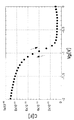
次に、上記の手順で作製したメモリ膜130の特性を示す。図3及び図4は、メモリ膜130の容量と電圧の関係を示すグラフである。図3は、Vgを+3Vから−3Vに走査し、その後再び+3Vに走査したときの特性である。図4は、Vgを+1Vから−1Vに走査し、その後再び+1Vに走査したときの特性である。図3及び図4中、Vgはシリコン基板111に対して電極ポリシリコン膜116に印加した電圧を、Cは単位面積あたりの静電容量を示す。図3からVgが−3Vになるとメモリ膜に書き込みが行われ、グラフが右にシフトし、ヒステリシス特性が現れることが分かった。なお、図示しないが、Vgが+3Vになるとグラフが元に戻ることから、消去が行われることが分かった。一方、図4からVgが±1Vの範囲内ではヒステリシス特性が現れず、書き込みも消去も行われないことが分かった。上記メモリ膜130を作製する手順を用いた場合、上記特性が再現性よく現れた。
【0072】
なお、書き込み・消去が行われ始める電圧はポリシリコン膜113の酸化量により変化した。上記の例ではポリシリコン膜113の酸化量は2nmであったが、この酸化量を1.5nmにしたときは、Vgを−1.5Vにすると書き込みが行われ、Vgを1.5Vにすると消去が行われた。このとき、Vg=±0.5Vでは書き込みも消去も行われなかった。
【0073】
図5及び図6は、本実施の形態であるメモリ膜113の詳細な断面図である。図5は、第1のシリコン微粒子114及び第2のシリコン微粒子115を熱酸化してメモリ膜130を作製した場合の断面図である。図6は、第1のシリコン微粒子114及び第2のシリコン微粒子115を熱酸化するのに代えて、CVD法により酸化膜を堆積してメモリ膜130′を作製した場合の断面図である。図5(b)及び図6(b)は、それぞれ図5(a)及び図6(a)の拡大図である。図5(b)と図6(b)とを比較すれば分かるように、電極ポリシリコン膜116と酸化膜112Bとの界面は、第1のシリコン微粒子114及び第2のシリコン微粒子115を熱酸化した場合の方が、第1のシリコン微粒子114及び第2のシリコン微粒子115にCVD法により酸化膜を堆積した場合よりも、凹凸が著しい。
【0074】
なお、基板としてシリコン基板を用いているが、半導体であればこの限りではない。また、電極ポリシリコン膜116の材質はこれに限らず、ゲルマニウム、ガリウム砒素などの半導体や、アルミニウム、銅、銀、金などの金属でもよく、導電性を有すれば良い。
【0075】
シリコン基板111上には、シリコン酸化膜112を介してポリシリコン膜113が形成されている。ポリシリコン膜113と電極ポリシリコン膜116との間には、シリコン酸化膜112Bがあり、このシリコン酸化膜112B中には、シリコン微粒子が形成されている。このポリシリコン微粒子は、その位置によって二種類に分けることができる。一方は、ポリシリコン膜113の近くにある第1のシリコン微粒子114である。他方は、シリコン微粒子114の斜め上方に位置する第2のシリコン微粒子115である。
【0076】
なお、ポリシリコン膜113、第1のシリコン微粒子114及び第2のシリコン微粒子115の材質はこれに限らず、ゲルマニウム、ガリウム砒素などの半導体や、アルミニウム、銅、銀、金などの金属でもよく、導電性の物質であれば良い。また、シリコン酸化膜112,112Bの材質はこれに限らず、シリコン窒化膜、シリコン酸化膜とシリコン窒化膜の積層膜、金属酸化膜など、電気絶縁性の物質であれば良い。シリコン基板111とポリシリコン膜113とに挟まれたシリコン酸化膜112の厚さは、例えば1nm〜6nmとすることが好ましく、ポリシリコン膜113の厚さは、例えば0.5nm〜10nmとすることが好ましく、第1のシリコン微粒子114及び第2のシリコン微粒子115の直径は、例えば2nm〜10nmとすることが好ましいが、それぞれこの限りではない。ただし、シリコン基板111とポリシリコン膜113とに挟まれたシリコン酸化膜112の厚さは、あまり薄いと電荷がトンネル現象でシリコン酸化膜を透過する確率が増して記憶保持時間が減少し、あまり厚いと短チャネル効果が増して素子の微細化が困難となるので、2nm〜5nmとするのがより望ましい。更にまた、第1のシリコン微粒子114及び第2のシリコン微粒子115の直径は、あまり小さいと量子サイズ効果が大きくなって、電荷の移動に大きな電圧が必要となり、あまり大きいと短チャネル効果が増して素子の微細化が困難となるので、3nm〜7nmとするのがより望ましい。
【0077】
シリコン微粒子を含むシリコン酸化膜の厚さ(すなわち、電極ポリシリコン膜116とシリコン微粒子を含むシリコン酸化膜112Bとの界面と、ポリシリコン膜113とシリコン微粒子を含むシリコン酸化膜112Bとの界面との間の距離)Wは、次式を満たすのが望ましい。
W≦2H+S1 …(1)
【0078】
ここで、Hはシリコン微粒子の平均直径または平均高さ、S1は第1のシリコン微粒子114とポリシリコン膜113とを隔てるシリコン酸化膜厚である。例として、Hが5nm、S1が2nmのとき、(1)式によるとWは12nm以下となる。(1)式は、第2のシリコン微粒子115の多くが第1のシリコン微粒子114の斜め上方に位置するときに満たされる。(1)式を満たすことにより、メモリ膜130,130′の実効的な厚さを薄くすることができ、メモリ膜130の静電容量を増加することが可能になる。
【0079】
ここで、シリコン微粒子の平均直径または平均高さHを評価するには、シリコン微粒子が10個程度以上写っている断面TEM(透過電子顕微鏡)写真を用い、この断面TEM写真に写っているシリコン微粒子の直径または高さを平均すればよい。また、シリコン微粒子を含むシリコン酸化膜112Bの厚さWを評価するには、電極ポリシリコン膜116と酸化膜112Bとの界面の凹凸が激しいときには、その平均値WAVを用いる。WAVを求めるには、シリコン微粒子が10個程度以上写っている断面TEM写真を用い、この断面TEM写真内での平均膜厚を採用すればよい。上記実施の形態で形成したメモリ膜130,130′の断面TEM写真を用いて上記解析を行ったところ、シリコン微粒子の高さの平均Hは5nm、第1のシリコン微粒子114とポリシリコン膜113とを隔てるシリコン酸化膜厚S1は2nmであり、シリコン微粒子を含むシリコン酸化膜112Bの厚さWAVは8nmであり、(1)式を満たしていた。
【0080】
本実施の形態のメモリ膜の製造方法によれば、シリコン微粒子の形成位置の制御は全く必要とせず、熱酸化工程とLPCVD工程の繰り返しで形成することができる。しかしながら、各ノード(ポリシリコン膜113、第1のシリコン微粒子114、第2のシリコン微粒子115及び電極ポリシリコン膜116)を隔てる酸化膜厚S1,S2,S3を、それぞれ精密に制御することが可能である。したがって、簡単な工程で電気特性が安定したメモリ膜を形成することが可能である。
【0081】
更にまた、メモリ特性の測定によれば、例えば、±3Vでの書き込み及び消去、1Vでの非破壊読み出しが可能であることが示され、従来技術のフラッシュメモリのメモリ膜に比べて著しく低電圧動作が可能であることが分かった。また、低電圧動作が可能なため、従来技術のフラッシュメモリで問題となっていた、高エネルギーの電荷によるメモリ膜の劣化を抑制し、信頼性を向上することができる。
【0082】
本実施の形態で作製されたメモリ膜130,130′は、シリコン微粒子114,115が斜めに並んでいるので、メモリ膜130,130′の厚さを薄くして、静電容量を大きくすることができる。したがって、例えば、このメモリ膜130,130′を電界効果トランジスタのゲート絶縁膜中に導入した場合、実効的なゲート絶縁膜厚を薄くすることができ、短チャネル効果を抑制し、メモリ素子の微細化が可能となる。
【0083】
(実施の形態2)
本発明の実施の形態2を、図7〜図9を用いて説明する。本実施の形態は、上記実施の形態1において、LPCVD法によるシリコン成長の回数(実施の形態1では3回)を変えたときのメモリ膜特性に関するものである。なお、シリコン基板の酸化、ポリシリコン膜の酸化及びシリコン微粒子の酸化はいずれも熱酸化としたものである。
【0084】
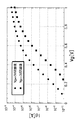
図7は、LPCVD法によるシリコン成長を1回行ったときのメモリ膜の容量と電圧の関係を示すグラフである。シリコン基板に対する電極ポリシリコン膜の電位Vgを、+3Vから−3Vに走査し、その後再び+3Vに走査した。メモリ効果は全く現れていない。このとき、メモリ膜の構造は、電極ポリシリコン膜/酸化膜/ポリシリコン膜/酸化膜/シリコン基板となっていた。
【0085】
図8は、LPCVD法によるシリコン成長を2回行ったときのメモリ膜の容量と電圧の関係を示すグラフである。ヒステリシスが現れ、メモリ効果が認められる。このとき、メモリ膜の構造は、図5において第2のシリコン微粒子115がなく、その分シリコン微粒子を含むシリコン酸化膜112の厚さが薄くなった構造であった。
【0086】
図9は、LPCVD法によるシリコン成長を3回行ったときのメモリ膜の容量と電圧の関係を示すグラフである。図8に比べてメモリ効果は非常に顕著である。なお、図示しないが、LPCVD法によるシリコン成長を4回行ったときの特性も、3回行った場合に近かった。
【0087】
以上のことから、LPCVD法によるシリコン成長は少なくとも2回行う必要があり、3回以上行うことがより好ましいことが分かった。なお、5回以上行うとメモリ膜の実効的な膜厚がさらに厚くなる(静電容量が減少する)。このメモリ膜を電界効果トランジスタのゲート絶縁膜中に導入した場合、メモリ膜の実効的な膜厚が厚いと短チャネル効果の抑制が難しくなり、メモリ素子の微細化が難しくなるので、LPCVD法によるシリコン成長は3回〜4回とするのが最も好ましい。なお、LPCVD法によるシリコン成長の初回では、ポリシリコン膜が形成されるので、シリコン微粒子を形成するためのLPCVD法によるシリコン成長は少なくとも1回以上行う必要があり、2回〜3回とするのが最も好ましい。
【0088】
(実施の形態3)
本発明の実施の形態3を、図10を用いて説明する。本実施の形態は、上記実施の形態1のメモリ膜と同じ形態のものを形成する別の方法に関する。
【0089】
図10は、図5に示すメモリ膜130と同じ形態のものを形成するための別の製造手順を示す図である。まず、シリコン基板111上に、900℃のN2O雰囲気中で、厚さ2nmのシリコン酸化膜112を形成した。なお、このシリコン酸化膜112の形成にはCVD法を用いることもできるが、ゲート酸化膜として電界効果トランジスタを形成する場合は界面準位の少ない熱酸化法によるのが好ましい。
【0090】
次に、この上に、分子線エピタキシ法(MBE法)またはLPCVD法で厚さ6nmのアモルファスシリコン膜121を形成した(図10(a))。この後、表面を弗化水素酸で洗浄してから超高真空CVD装置に入れてSi2H6 を供給する方法(第1の方法)と、アモルファスシリコン膜形成後、大気開放せずに、Si2H6 を供給する方法(第2の方法)とがある。
【0091】
まず、第1の方法を説明する。アモルファスシリコン膜121の形成後、その状態の基板を、NH4 OH、H2O2 およびH2Oを1:6:20の割合で混合した洗浄液(60℃)に浸して表面の汚染を除去し、5%弗化水素酸水溶液に30秒間浸して自然酸化膜を除去した。次に、その状態の基板を、遠心分離器または乾燥窒素ガスにより乾燥させ、Si2H6 供給用のノズルとグラファイトヒータによる基板加熱装置とを備えた超高真空CVD装置の形成室内に入れた。形成室内の真空度は10−9Torrに保たれている。まず、ある一定の温度、好ましくは加熱のみによる核形成が急速に起こらないような、500℃ないし620℃という低温で基板加熱を行い、そのあと核形成用のSi2H6を流量13cccmで照射すると、アモルファスシリコン膜121の表面に結晶核122が発生した(図10(b))。このとき、アモルファスシリコン膜121の表面に沿った平面内では、結晶核122の形成位置は実質的にランダムであった。結晶核の形成密度は、Si2H6の照射時間にほぼ比例して増加した。また、このとき、結晶核の直径はSi2H6の照射時間によらずほぼ一定であった。一定時間Si2H6ガスに曝らしたのち、高真空にして加熱を続行し結晶核122の成長を行った。なお、この高真空中での加熱は結晶核のサイズを調節するためのものであり、省略することもできる。また、Si2H6ガスの照射においては、SiH4ガスを用いてもよく、又はSi2H6ガスとSiH4ガスを混合したものでもよい。この後、後述の熱酸化工程を行った。
【0092】
次に、第2の方法を説明する。アモルファスシリコン膜121の形成後、大気開放せずに基板温度を500℃ないし620℃とし、そのあと核形成用のSi2H6を流量13cccmで照射すると、第1の方法の場合と同様に、アモルファスシリコン膜121の表面に結晶核122が発生した(図10(b))。結晶核の形成密度は、Si2H6の照射時間にほぼ比例して増加した。また、このとき、結晶核の直径はSi2H6の照射時間によらずほぼ一定であった。一定時間Si2H6ガスに曝らしたのち、高真空にして加熱を続行し結晶核122の成長を行った。なお、この高真空中での加熱は結晶核のサイズを調節するためのものであり、省略することもできる。また、Si2H6ガスの照射においては、SiH4ガスを用いてもよく、又はSi2H6ガスとSiH4ガスを混合したものでもよい。この後、後述の熱酸化工程を行った。
【0093】
上記第1の方法または第2の方法で述べた工程を行った後、900℃のN2O雰囲気中で、熱酸化を行った。その結果、アモルファスシリコン膜121の一部と、結晶核122の一部は酸化されてシリコン酸化膜124となった。また、アモルファスシリコン膜121の一部は酸化されずポリシリコン膜123となった。さらに、結晶核122の中心部は酸化されず、第1のシリコン微粒子125となった。
【0094】
この後の手順は、実施の形態1における第2のシリコン微粒子形成工程以降の手順と同じである。かくして、上記方法によっても図5に示すメモリ膜130と同じ形態のものを形成することができた。
【0095】
本実施の形態となるメモリ膜の製造方法は、シリコン微粒子の形成位置の制御は全く必要とせず、熱酸化工程とLPCVD工程またはMBE工程の繰り返しで形成することができる。しかしながら、各ノード(ポリシリコン膜123、第1のシリコン微粒子125、第2のシリコン微粒子及び電極ポリシリコン膜)を隔てる酸化膜厚を、それぞれ精密に制御することが可能である。したがって、簡単な工程で電気特性が安定したメモリ膜を形成することが可能である。
【0096】
また、本実施の形態となるメモリ膜の製造方法によると、Si2H6 の供給時間を変化させるだけでシリコン微粒子の形成密度を制御することができる。したがって、メモリ膜の特性を制御するのが容易となる。
【0097】
(実施の形態4)
本発明の実施の形態4を、図11及び図12を用いて説明する。本実施の形態のメモリ素子は、実施の形態1のメモリ膜130または130′を電界効果トランジスタのゲート絶縁膜に組み込んで構成したものである。
【0098】
図11は、本実施の形態であるメモリ素子の断面図である。シリコン基板111上に、図6に示すメモリ膜130′を介して電極ポリシリコン116(ゲート電極)が形成されている。また、ソース領域117とドレイン領域118が形成されている。
【0099】
なお、本実施の形態では、シリコン基板111はP型の導電型を持ち、ゲート電極、ソース領域及びドレイン領域はN型の導電型を持っており、Nチャネル型の電界効果トランジスタとなっている。しかし、これに限らず、Pチャネル型の電界効果トランジスタ(N型のシリコン基板と、P型のソース領域及びドレイン領域を持つ)であっても良いし、ゲート電極はポリシリコンに限らず、金属であっても良い。また、図11に示すメモリ素子は、図6に示すメモリ膜130′を用いているが、図5に示すメモリ膜130を用いても良い。
【0100】
本実施の形態のメモリ素子は、実施の形態1のメモリ膜130または130′を用いているので、実効的なゲート絶縁膜厚を薄くすることができる。したがって、短チャネル効果を抑制し、素子の微細化が可能である。
【0101】
更に、本実施の形態のメモリ素子は、実施の形態1のメモリ膜130または130′を用いているので、低電圧での書き込み及び消去及び非破壊読み出しが可能である。具体的には、例えば、ポリシリコン膜113の酸化量が2nmのときは±3Vでの書き込み・消去が、1Vでの非破壊読み出しが可能である。また、ポリシリコン膜113の酸化量が1.5nmのときは±1.5Vでの書き込み・消去が、0.5Vでの非破壊読み出しが可能である。したがって、低電圧動作が可能で、低消費電力化が可能となり、素子の信頼性が向上する。
【0102】
本実施の形態のメモリ素子を製造する手順は、電界効果トランジスタを作製する公知の手順とほぼ同じである。公知の手順と異なるのは、メモリ膜の形成においてのみであり、メモリ膜を形成する手順は実施の形態1〜3のいずれかに記載した通りである。
【0103】
実施の形態1又は2の製造手順によれば、メモリ膜部分の形成にあたって、4回の熱酸化工程と3回のLPCVD工程を繰り返しただけであり、シリコン微粒子の形成位置の制御は全く必要としない。しかしながら、ポリシリコン膜113と第1のシリコン微粒子114とを隔てる酸化膜厚S1、第1のシリコン微粒子114と第2のシリコン微粒子115とを隔てる酸化膜厚S2、第2のシリコン微粒子115と電極ポリシリコン膜116とを隔てる酸化膜厚S3を、それぞれ精密に制御することが可能である。したがって、簡単な工程で電気特性が安定したメモリ素子を形成することが可能である。
【0104】
実施の形態3の製造手順によれば、シリコン微粒子の形成位置の制御は全く必要とせず、熱酸化工程とLPCVD工程またはMBE工程の繰り返しで形成することができる。しかしながら、各ノード(ポリシリコン膜123、第1のシリコン微粒子125、第2のシリコン微粒子及び電極ポリシリコン膜)を隔てる酸化膜厚を、それぞれ精密に制御することが可能である。したがって、簡単な工程で電気特性が安定したメモリ膜を形成することが可能である。
【0105】
また、実施の形態3の製造手順によれば、Si2H6 の供給時間を変化させるだけでシリコン微粒子の形成密度を制御することができる。したがって、メモリ膜の特性を制御するのが容易となる。
【0106】
次に、上記の手順で作製したメモリ素子の特性を示す。図12は、メモリ素子のドレイン電流(Id)とゲート電圧(Vg)との関係を示すグラフである。ゲート電極に−3Vを印加した後は、閾値が高くなっており(書き込み)、メモリ効果を示すことが分かる。一方、ゲート電極に+3Vを印加すると、閾値は低くなり、消去が行われることが分かった。
【0107】
本実施の形態のメモリ素子は、実施の形態1のメモリ膜130または130′を用いているので、実効的なゲート絶縁膜厚を薄くすることができる。したがって、短チャネル効果を抑制し、素子の微細化が可能である。
【0108】
更に、本実施の形態のメモリ素子は、実施の形態1のメモリ膜130または130′を用いているので、±3Vでの書き込み及び消去、1Vでの非破壊読み出しが可能である。したがって、従来技術のフラッシュメモリに比べて著しい低電圧動作が可能で、低消費電力化が可能となり、素子の信頼性が向上する。
【0109】
また、本実施の形態のメモリ素子は、メモリ膜の形成に実施の形態1または2に示した手順を用いればよいので、シリコン微粒子の形成位置の制御は全く必要とせず、熱酸化工程とLPCVD工程(またはMBE工程)の繰り返しで形成することができる。しかしながら、各ノード(ポリシリコン膜、第1のシリコン微粒子、第2のシリコン微粒子及び電極ポリシリコン膜)を隔てる酸化膜厚を、それぞれ精密に制御することが可能である。したがって、簡単な工程で電気特性が安定したメモリ素子を形成することが可能である。
【0110】
(実施の形態5)
本発明の実施の形態5を、図13を用いて説明する。本実施の形態のメモリ素子は、実施の形態4のメモリ素子を、SOI(Silicon on Insulator)基板150上に形成したものである。図13は、本実施の形態の半導体装置におけるメモリ素子の断面図である。119はボディ、120は埋め込み酸化膜である。また、図13に示すメモリ素子は、図6に示すメモリ膜130′を用いているが、図5に示すメモリ膜130を用いても良い。なお、図13では、完全空乏型の場合を示しているが、部分空乏型にしてもよい。
【0111】
本実施の形態のメモリ素子を製造する手順は、SOI基板上に電界効果トランジスタを作製する公知の手順とほぼ同じである。公知の手順と異なるのは、メモリ膜の形成においてのみであり、メモリ膜を形成する手順は実施の形態1〜3のいずれかに記載した通りである。
【0112】
本実施の形態の半導体装置においては、実施の形態4のメモリ素子で得られる効果に加えて以下の効果が得られる。本実施の形態のメモリ素子においては、ソース領域117及びドレイン領域118と、ボディ119との接合容量を非常に小さくすることができる。さらにまた、SOI基板を用いると、ソース領域117及びドレイン領域118の深さを浅くするのが容易であり、短チャネル効果を抑制し、素子を更に微細化することができる。
【0113】
(実施の形態6)
本発明の実施の形態6について、図14〜図18に基づいて説明すれば以下の通りである。
【0114】
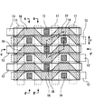
図14〜図17は、本発明の実施の形態6となるメモリセルアレイの概略図である。図14は、平面の概略図である。図15は図14の切断面線A−A’から見た断面図であり、図16は図14の切断面線B−B’から見た断面図であり、図17は図14の切断面線C−C’から見た断面図である。図18は、上記メモリセルアレイの回路図である。
【0115】
まず、本実施の形態の半導体装置の構成を図14〜図17に基づいて説明する。図15〜図17から分かるように、シリコン基板17内にはN型の深いウェル領域25とP型の浅いウェル領域26が形成されている。さらに、複数の素子分離領域16が、図14における横方向に蛇行して延びるように形成されている(図14中で、それぞれ蛇行した帯状の領域に斜線を施している。)。素子分離領域16の縦方向のピッチは2F(Fは最小加工ピッチ)に設定されている。これにより、ウェル領域26の上部で隣り合う素子分離領域16の間に、それぞれ横方向に蛇行して延びるシリコン活性領域が残されている。素子分離領域16の深さは、素子分離領域16をはさむ両側のP型の浅いウェル領域26が互いに電気的に分離されるように設定される。
【0116】
図14〜図17を総合すれば分かるように、上記各シリコン活性領域内の蛇行の各折り返し箇所に、それぞれ不純物拡散領域としてのN+拡散層19が形成されている。各N+拡散層19は、このメモリの使用時にビット線による選択に応じてソース領域またはドレイン領域として働く。その時、同一の活性領域内で隣り合うN+拡散層19の間の領域がそれぞれチャネル領域となる。
【0117】
ポリシリコンからなる複数のワード線11が、素子分離領域16が延びる方向とは垂直方向(図14における縦方向)にストレートに延びるように形成されている。ワード線11の横方向のピッチは2Fに設定されている。ワード線11で覆われているシリコン活性領域(ウェル領域26の上部)は、チャネル領域となっている。チャネル領域とワード線11とは、実施の形態1の図5もしくは図6で示したメモリ膜と同じ構成のメモリ膜21により隔てられている。このチャネル領域上でワード線11がコントロールゲートの役割をはたしている。
【0118】
第1層メタルからなる複数の第1ビット線12が、ワード線11とは垂直方向(図14における横方向)にストレートに延びるように形成されている。第1ビット線12の縦方向のピッチは2Fに設定され、同一のシリコン活性領域内で蛇行の片側(図14では山側)の折り返し箇所に設けられたN+拡散層19上を通るように設けられている。この第1ビット線12とその直下に存するN+拡散層19とは、横方向に関してピッチ4Fで、第1ビット線コンタクト14により接続されている。また、第2層メタルからなる複数の第2ビット線13が、第1ビット線12と同じ方向で第1ビット線の隙間となる位置に、第1ビット線と平行にストレートに延びるように形成されている。第2ビット線13の縦方向のピッチは2Fに設定されて、同一のシリコン活性領域内で蛇行の他方の側(図14では谷側)の折り返し箇所に設けられたN+拡散層19上を通るように設けられている。この第2ビット線13とその直下に存するN+拡散層19とは、横方向に関してピッチ4Fで、第2ビット線コンタクト15により接続されている。第1および第2のビット線12,13は、互いに層間絶縁膜20で分離され、上述のようにそれぞれ必要なところでコンタクト14,15を介してN+拡散層19と接続されている。また、シリコン基板に対してP型の浅いウェル領域26は、素子分離領域16によって、第1ビット線及び第2ビット線と同じ方向に走る細長い列状に分断されており、第3ビット線を構成している。
【0119】
上記構成によれば、1つのメモリセルは図14中に二点鎖線で示す平行四辺形22で表され、その面積は4F2である。
【0120】
なお、メモリ膜21は、図5もしくは図6におけるシリコン酸化膜112、シリコン酸化膜112B、ポリシリコン膜113、第1のシリコン微粒子114及び第2のシリコン微粒子115からなる膜である。
【0121】
次に、本実施の形態であるメモリセルアレイの回路構成を、図18に基づいて説明する。このメモリセルアレイは、いわゆるAND型で配列されている。すなわち、一本の第1ビット線と一本の第2ビット線とが一対をなしており、これらのビット線の間にn個のメモリセルが並列に接続されている。図18では、例えば1番目のビット線対の第1ビット線をBa1、1番目のビット線対の第2ビット線をBb1と表記している。また、例えば1番目のビット線対に接続されているn番目のメモリセルをM1nと表記している。各ビット線には選択トランジスタが設けられている。図18では、例えば1番目のビット線対の第1ビット線選択トランジスタをSTBa1と表記している。本実施の形態であるメモリセルアレイの特徴は、P型の浅いウェル領域が第3ビット線を形成している点である。この第3ビット線は、第1ビット線及び第2ビット線からなる1対のビット線に並列に接続されたメモリセルの浅いウェル領域を接続している。この第3ビット線には選択トランジスタが接続されている。図18では、例えば、1番目の第3ビット線はBw1、それに対応する選択トランジスタはSTBw1と表記されている。また、n本のワード線が、各ビット線と垂直方向に走り、メモリセルのゲート間を接続している。図18では、各ワード線をW1〜Wnで表記している。
【0122】
次に、本実施の形態のメモリセルアレイを作製する手順を説明する。
【0123】
まず、図15〜図17中に示すシリコン基板17内に電気絶縁性の素子分離領域16を形成し、続いてN型の深いウェル領域25とP型の浅いウェル領域26を形成する。N型の深いウェル領域とP型の浅いウェル領域との接合の深さは、不純物の注入条件(注入エネルギーと注入量)とその後の熱工程(アニール工程や熱酸化工程など)によって決まる。これら不純物注入条件や熱工程条件と、素子分離領域の深さは、素子分離領域16がP型の浅いウェル領域26を電気的に分離するように設定される。
【0124】
その後、実施の形態1〜3のいずれかで示した手順でメモリ膜21を形成し、フォトリソグラフィとエッチングによりパターン加工する。このパターン加工後、メモリ膜中のポリシリコン膜が露出し、後に形成するワード線と短絡する恐れがあるので、熱酸化を行うのが好ましい。その後、ポリシリコン膜を、化学的気相成長法(CVD法)で形成し、このポリシリコン膜とメモリ膜21とをフォトリソグラフィとエッチングによりパターン加工し、ワード線11を形成する。ここで、N型の不純物を、ワード線11をマスクとして低エネルギで注入すると、自己整合的にN+拡散層19が形成される。この後、層間絶縁膜の堆積、コンタクト工程、メタル工程を繰り返し行い、第1ビット線12及び第2ビット線13を形成する。
【0125】
本実施の形態のメモリセルアレイは、実施の形態1〜3のいずれかで示したメモリ膜を用いている。したがって、素子の微細化が可能であるため高集積化が実現される。更には低電圧駆動が可能であるから、低消費電力化が可能となり、メモリセルアレイの信頼性が向上する。
【0126】
更にまた、本実施の形態のメモリセルアレイは、1つのセルの面積が4F2であり、従来のAND型メモリセルアレイ(セルの面積が8F2程度)よりも小さい。したがって、高集積化が可能となり、製品の歩留りが向上し、製造コストを削減することができる。
【0127】
また、本実施の形態の半導体装置であるメモリと、論理回路、その他のメモリ(DRAM、SRAM等)とを混載した場合、集積回路の集積度を向上し、機能の向上を図ることができる。
【0128】
(実施の形態7)
本実施の形態は、実施の形態6のメモリセルアレイにおいて、選択されたメモリセルのメモリ膜にかかる電圧と、非選択のメモリセルのメモリ膜にかかる電圧の比をできる限り大きくした、ランダムアクセスが可能なメモリセルアレイに関する。
【0129】
一般に、メモリセルの書き込み時または消去時には、選択されたメモリセルのメモリ膜に最大の電圧がかかる。そして、非選択のメモリセルのメモリ膜にもある程度の電圧がかかってしまう。したがって、誤動作を防ぐためには、選択されたメモリセルのメモリ膜にかかる電圧と、非選択のメモリセルのメモリ膜にかかる電圧の最大値との比をできるだけ大きくするのが好ましい。
【0130】
一般的に行われている方法では、例えば消去時には、選択ワード線の電位をVDDに、選択ビット線の電位を接地電位に、その他のワード線及びビット線の電位をVDD/2にする。このとき、選択されたメモリセルのメモリ膜には電圧VDDが、非選択のメモリセルのメモリ膜には電圧0またはVDD/2がかかる。このとき、選択されたメモリセルのメモリ膜にかかる電圧と、非選択のメモリセルのメモリ膜にかかる電圧の最大値との比は1/2である。
【0131】
本実施の形態のメモリセルアレイにおける、書き込み時及び消去時の各ワード線及びビット線への印加電圧を表1に示す。なお、各ビット線(第1〜第3ビット線)には、同電位を与える。書き込み時には、選択ワード線に電位0、非選択ワード線に(1−A)×VDD、選択ビット線にVDD、非選択ビット線にA×VDDを印加する。また、消去時には、選択ワード線に電位VDD、非選択ワード線にA×VDD、選択ビット線に0、非選択ビット線に(1−A)×VDDを印加する。ここで、1/3≦A<1/2である(A=1/2のときは、上記一般的に行われている例となる)。選択されたメモリセルのメモリ膜にかかる電圧と、非選択のメモリセルのメモリ膜にかかる電圧の最大値との比は、A=1/3のとき(絶対値で)最大値3をとる。したがって、A=1/3とするのがもっとも好ましい。
【表1】

上記のように印加電圧を設定することにより、1ビット毎の書き込み動作及び消去動作、すなわちランダムアクセスが可能となる。VDDの具体的な値は、膜質や膜構造ごとに最適な値を決めればよい。具体的には、メモリ膜にかかる電圧の絶対値がVDDのときには電荷の注入または放出が起こり、メモリ膜にかかる電圧の絶対値がA×VDDのときには電荷の注入または放出が起こらないようにする。なお、読み出し時には、メモリ膜にかかる電圧がA×VDD以下となるようにするのが好ましく、その場合、読み出しにより記憶を破壊することがない。
【0133】
本実施の形態のメモリセルアレイにおいては、選択されたメモリセルのメモリ膜にかかる電圧と、非選択のメモリセルのメモリ膜にかかる電圧の最大値との比が大きく、ランダムアクセスが可能で、動作マージンの大きなメモリを実現することが可能となる。
【0134】
(実施の形態8)
本発明の実施の形態8について、図19に基づいて説明すれば以下の通りである。本実施の形態のメモリセルアレイは、実施の形態6又は7のいずれかのメモリセルアレイにおいて、SOI基板160を用いて作製したもので、その平面図は図14と同じである。36はボディ、35は埋め込み酸化膜である。図19は、本実施の形態となるメモリセルアレイのメモリセル断面の模式図である。素子分離領域16と埋め込み酸化膜35とで分離されたボディ36の列にそれぞれ独立した電位を与え、第3ビット線として用いる。なお、図19では、完全空乏型の場合を示しているが、部分空乏型にしてもよい。その場合は、第3ビット線となるボディの抵抗を低減して素子の高速化が可能となる。
【0135】
次に、本実施の形態の半導体装置を作製する手順を説明する。まず、SOI基板160に素子分離領域16を形成する。その後、メモリ素子が適切な閾値をもつように、ボディ36に不純物注入を行う。これ以降の上部構造の形成は、実施の形態5で示した手順と同様である。
【0136】
本実施の形態の半導体装置においては、実施の形態6又は7のメモリセルアレイで得られる効果に加えて以下の効果が得られる。本実施の形態の半導体装置においては、厚い埋め込み酸化膜の存在のために、ボディとシリコン基板との間の静電容量を非常に小さくすることができる。一方、実施の形態6又は7のメモリセルアレイでは、浅いウェル領域と深いウェル領域との間の静電容量はかなり大きい。また、SOI基板を用いると、N+活性層とボディとの接合容量を非常に小さくすることができる。そのため、本実施の形態のメモリセルアレイにおいては、容量を充電するための消費電流を小さくすることができる。さらにまた、SOI基板を用いると、N+活性層の深さを浅くするのが容易であり、短チャネル効果を抑制し、素子を更に微細化することができる。以上の理由から、SOI基板を用いることにより、低消費電力化及び微細化が可能となる。
【0137】
(実施の形態9)
上記実施の形態1〜8のメモリ素子又は半導体記憶装置を集積化して集積回路とすれば、低電源電圧で動作させることが可能になり、集積回路を低消費電力化できる。
【0138】
また、上記実施の形態4〜8のメモリ素子又は半導体記憶装置と、論理回路とを1つの集積回路上に混載してもよい。更に、メモリ素子又は半導体記憶装置と、論理回路とに加え、その他のメモリ(DRAM、SRAM等)も混載しても良い。例えば、実施の形態6〜8のメモリセルアレイを用いれば、セル面積は4F2であり、通常の1トランジスタ型不揮発性メモリのメモリセル面積より小さい。したがって、メモリが占める面積を小さくできる分、論理回路や他のメモリの面積を大きくとることができ、機能の向上を図ることができる。もしくは、本実施の形態の半導体装置であるメモリの記憶容量を大きくとることができる。その場合、例えば、大規模なプログラムを一時的に読みこみ、電源を切断した後もそのプログラムを保持し、電源を再投入した後もプログラムを実行するといったことが可能になり、かつ、そのプログラムを他のプログラムと入れかえることもできる。
【0139】
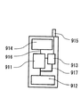
また、上記集積回路を、電池駆動の携帯電子機器に組み込むことができる。携帯電子機器としては、携帯情報端末、携帯電話、ゲーム機器などが挙げられる。図20は、携帯電話の例を示している。制御回路911には、本発明の半導体集積回路が組み込まれている。なお、制御回路911は、本発明の半導体装置からなるメモリ回路と、論理回路とを混載したLSIから成っていてもよい。912は電池、913はRF回路部、914は表示部、915はアンテナ部、916は信号線、917は電源線である。本発明の半導体集積回路を携帯電子機器に用いることにより、携帯電子機器を高機能化し、LSI部の消費電力を大幅に下げることが可能になる。それにより、電池寿命を大幅にのばすことが可能になる。
【0140】
【発明の効果】
以上より明らかなように、本発明によれば、低電圧で動作可能なメモリ膜およびその製造方法を提供することができる。また、本発明によれば、そのようなメモリ膜を有するメモリ素子を提供することができる。さらに、本発明によれば、そのようなメモリ素子を有する半導体記憶装置、半導体集積回路および携帯電子機器を提供することができる。
【図面の簡単な説明】
【図1】 本発明の実施の形態1のメモリ膜の製造方法を示す図である。
【図2】 本発明の実施の形態1のメモリ膜の製造方法を示す図である。
【図3】 本発明の実施の形態1のメモリ膜にかける電圧を走査したときの容量の変化を示すグラフである。
【図4】 本発明の実施の形態1のメモリ膜にかける電圧を走査したときの容量の変化を示すグラフである。
【図5】 本発明の実施の形態1のメモリ膜の断面図である。
【図6】 本発明の実施の形態1のメモリ膜の断面図である。
【図7】 メモリ膜の形成時にLPCVD法によるシリコン成長を1回行った場合の、メモリ膜にかける電圧を走査したときの容量の変化を示すグラフである。
【図8】 メモリ膜の形成時にLPCVD法によるシリコン成長を2回行った場合の、メモリ膜にかける電圧を走査したときの容量の変化を示すグラフである。
【図9】 メモリ膜の形成時にLPCVD法によるシリコン成長を3回行った場合の、メモリ膜にかける電圧を走査したときの容量の変化を示すグラフである。
【図10】 本発明の実施の形態3のメモリ膜の製造方法を示す図である。
【図11】 本発明の実施の形態4のメモリ素子の断面図である。
【図12】 本発明の実施の形態4のメモリ素子の、書き込み時及び消去時のドレイン電流対ゲート電圧の関係を示すグラフである。
【図13】 本発明の実施の形態5のメモリ素子の断面図である。
【図14】 本発明の実施の形態6のメモリセルアレイの平面図である。
【図15】 図14の切断面線A−A’から見た断面図である。
【図16】 図14の切断面線B−B’から見た断面図である。
【図17】 図14の切断面線C−C’から見た断面図である。
【図18】 本発明の実施の形態6のメモリセルアレイの回路図である。
【図19】 本発明の実施の形態8のメモリセルアレイのメモリセルの断面図である。
【図20】 本発明の実施の形態9の携帯情報機器の構成図である。
【符号の説明】
111 シリコン基板
112,112B シリコン酸化膜
113 ポリシリコン膜
114 第1のシリコン微粒子
115 第2のシリコン微粒子
116 電極ポリシリコン膜
130,130′,21 メモリ膜
150,160 SOI基板[0001]
BACKGROUND OF THE INVENTION
The present invention relates to a memory film, a manufacturing method thereof, a memory element, a semiconductor memory device, a semiconductor integrated circuit, and a portable electronic device. More specifically, the present invention relates to a memory film containing conductive fine particles, a manufacturing method thereof, and a memory element having such a memory film. The present invention also relates to a semiconductor memory device, a semiconductor integrated circuit, and a portable electronic device having such a memory element.
[0002]
[Prior art]
As a conventional technique in which a field effect transistor including a memory film that accumulates charges in a gate insulating film is used as a memory element, a flash memory can be cited. In a flash memory, a conductive film called a floating gate is provided in an insulating film between a control gate and a channel region. By injecting or emitting electrons from the channel region to the floating gate by FN (Fowler-Nordheim) tunneling, the amount of charge in the floating gate is changed, and a large amount of this amount of charge is held as stored information. In reading stored information, a large amount of charge in the floating gate can be detected as a difference in threshold values of the field effect transistors.
[0003]
[Problems to be solved by the invention]
However, the conventional technique has a problem that the operating voltage is high. As an operation example of the flash memory, for example, −8 V is applied to the selected word line and 6 V is applied to the selected bit line at the time of writing, and 10 V is applied to the selected word line and −8 V is applied to the bit line at the time of erasing. Since the operating voltage is high in this way, the power consumption during writing and erasing is large, which hinders the reduction in power consumption. Further, since a high electric field is applied to the gate insulating film, deterioration of the element has been a problem.
[0004]
The present invention has been made to solve the above problems, and an object of the present invention is to provide a memory film operable at a low voltage and a method for manufacturing the same. Another object of the present invention is to provide a memory element having such a memory film. Furthermore, an object of the present invention is to provide a semiconductor memory device, a semiconductor integrated circuit, and a portable electronic device having such a memory element.
[0005]
[Means for Solving the Problems]
In order to solve the above-described problem, a method for manufacturing a memory film according to the first invention includes:
Forming a first insulating film on a semiconductor substrate to be a first electrode;
Forming a first conductor film on the first insulating film;
Forming a second insulating film on the surface of the first conductor film;
Forming a third insulating film containing conductive fine particles on the second insulating film;
Forming a second conductor film serving as a second electrode on the third insulating film;
IncludingSee
The fine particles of the conductor contained in the third insulating film are
Fine particles of a first conductor proximate to the first conductor film;
The second conductor fine particles adjacent obliquely above the first conductor fine particles,
The positions of the fine particles of the first conductor projected onto the plane formed by the first conductor film are substantially random;
The diameter or height of the fine particles of the conductor is H,
The distance between the first conductor film and the fine particles of the first conductor is S 1 age,
When the average thickness of the third insulating film is W,
W ≦ 2H + S 1
Satisfy a relationshipIt is characterized by that.
[0006]
In this specification, the term “fine particles” means particles having dimensions of the order of nanometers (nm).
[0007]
According to the method for manufacturing a memory film of the first invention, the first conductor film is formed on the semiconductor substrate via the first insulating film, and the first conductor film is formed on the first conductor film. A third insulating film containing conductive fine particles is formed through the second insulating film, and the second conductive film is formed on the third insulating film. Therefore, the semiconductor substrate and the second conductor film serve as electrodes, respectively, and the first conductor film and the third insulating film containing fine particles of the conductor serve as a charge storage portion, and the memory film is formed. Constitute. The memory film thus formed can be written / erased and read nondestructively at a low voltage.
[0008]
The conductive fine particles contained in the third insulating film are adjacent to the first conductive fine particles close to the first conductive film and obliquely above the first conductive fine particles. The positions of the fine particles of the first conductor projected onto the plane formed by the first conductive film are substantially random. As a result, a memory film having a remarkable memory effect is obtained, and it is not necessary to control the positions of the fine particles of the conductor contained in the third insulating film. Therefore, a memory film having a remarkable memory effect can be manufactured by a simple process.
[0009]
The diameter or height of the fine particles of the conductor is H, and the distance between the first conductive film and the fine particles of the first conductor is S. 1 And when the average thickness of the third insulating film is W,
W ≦ 2H + S 1
Satisfy the relationship. When this relationship is satisfied, most of the fine particles of the second conductor are located obliquely above the fine particles of the first conductor, and few are located directly above. Therefore, the thickness of the memory film can be reduced and the capacitance can be increased. For example, when this memory film is introduced into the gate insulating film of a field effect transistor, the effective gate insulating film thickness can be reduced, the short channel effect can be suppressed, and the memory element can be miniaturized.
[0010]
In one embodiment, the step of forming a third insulating film containing conductive fine particles on the second insulating film includes the step of forming conductive fine particles on the second insulating film; A series of steps including a step of forming a third insulating film on the surface of the fine particles of the conductor is performed at least once.
[0011]
According to the embodiment, by performing the series of steps at least once, it is possible to cause a memory effect that is not seen when the series of steps is not performed.
[0012]
In one embodiment, the above-described series of steps is performed as 2CirculationIt is characterized by that.
[0013]
According to the embodiment described above, a remarkable memory effect can be obtained, and at the same time, the short channel effect can be suppressed and the device can be easily miniaturized.
[0014]
In one embodiment, the first conductor film is made of a semiconductor, the fine particles of the conductor are made of a semiconductor, a step of forming a first insulating film on the semiconductor substrate, and a surface of the conductor film Both the step of forming the second insulating film and the step of forming the third insulating film on the surface of the fine particles of the conductor are thermal oxidation steps, and the first conductive film is formed on the first insulating film. Both the step of forming the body film and the step of forming fine particles of the conductor on the second insulating film are characterized by chemical vapor deposition.
[0015]
According to the embodiment, the first conductor film and the fine particles of the conductor are both made of a semiconductor, and the step of forming the first insulating film, the second insulating film, and the third insulating film includes Both are thermal oxidation processes. The first conductor film and the fine particles of the conductor are both formed by chemical vapor deposition. That is, the memory effect appears with good reproducibility despite only repeating the thermal oxidation process and the chemical vapor deposition method. Therefore, it is possible to form a memory film with stable electrical characteristics by a simple process.
[0016]
In one embodiment, the first conductor film is a polycrystalline semiconductor or an amorphous semiconductor.
[0017]
According to the above embodiment, the conditions for forming the first conductive film can be the same as those for forming a floating gate of a widely manufactured flash memory. The conditions for forming the first conductive film can be used as they are in the step of forming conductive fine particles on the second insulating film. Therefore, it is possible to simplify the process and process conditions.
[0018]
In one embodiment, the semiconductor substrate is made of a silicon substrate, the first conductor film is made of silicon, the first to third insulating films are all made of a silicon oxide film, and the fine particles of the conductor are made. Are characterized by being made of silicon.
[0019]
According to the above embodiment, by using silicon that is most widely used as an LSI material, it is easy to mount an element using the memory film of the present invention with another element. Also, a very advanced silicon process can be used, which facilitates manufacturing.
[0020]
The method for manufacturing a memory film according to the second invention is as follows:
Forming a first insulating film on the semiconductor substrate;
Forming an amorphous semiconductor film on the first insulating film;
After the step of forming the amorphous semiconductor film, the step of opening the atmosphere and cleaning the amorphous semiconductor film;
Si on the amorphous semiconductor film2H6Gas or SiH4Introducing a gas containing one or both of the gases to generate semiconductor nuclei;
Of the amorphous semiconductor filmUpper partAnd of the above semiconductor nucleusSurface partIs thermally oxidized to form the first oxide filmAs a result, the first semiconductor film is formed from the lower part of the amorphous semiconductor film other than the upper part, and from the central part of the semiconductor nucleus other than the surface part.Forming a first semiconductor fine particle;
Forming a second conductor film on the first oxide film;
It is characterized by including.
[0021]
In the method of manufacturing the memory film of the second inventionAccording to the present invention, the semiconductor device includes a first insulating film, a first semiconductor film, a first oxide film containing fine particles of the first semiconductor, and a second conductor film.Memory film with structure can be formed.
[0022]
Furthermore, the Si2H6Gas or SiH4In the step of generating a semiconductor nucleus by introducing a gas containing one or both of the gases, the formation density of the silicon fine particles can be controlled only by changing the gas supply time. Therefore, it becomes easy to control the characteristics of the memory film.
[0023]
A method for manufacturing a memory film according to a third aspect of the invention includes:
Forming a first insulating film on the semiconductor substrate;
Forming an amorphous semiconductor film on the first insulating film;
After the step of forming the amorphous semiconductor film, the step of opening the atmosphere and cleaning the amorphous semiconductor film;
Si on the amorphous semiconductor film2H6Gas or SiH4Introducing a gas containing one or both of the gases to generate semiconductor nuclei;
Of the amorphous semiconductor filmUpper partAnd of the above semiconductor nucleusSurface partIs thermally oxidized to form the first oxide filmAs a result, the first semiconductor film is formed from the lower part of the amorphous semiconductor film other than the upper part, and from the central part of the semiconductor nucleus other than the surface part.Forming a first semiconductor fine particle;
Forming fine particles of a second conductor on the first oxide film;
Forming a third insulating film on the surface of the fine particles of the second conductor;
Forming a second conductor film on the third insulating film;
It is characterized by including.
[0024]
In the method of manufacturing the memory film of the third inventionAccording to the above, on the semiconductor substrate, the first insulating film, the first semiconductor film, the first oxide film containing the first semiconductor fine particles, and the second conductive film covered with the third insulating film. A memory film having a structure including a body fine particle and a second conductor film can be formed. In particular,Since the second conductor fine particles are formed in addition to the first semiconductor fine particles, the memory has the same structure as the case where the series of steps are performed twice in the first embodiment of the first invention. A film is formed. Therefore, a memory film having a remarkable memory effect can be obtained.Similarly to the method of manufacturing the memory film of the second invention, the Si film 2 H 6 Gas or SiH 4 In the step of generating a semiconductor nucleus by introducing a gas containing one or both of the gases, the formation density of the silicon fine particles can be controlled only by changing the gas supply time. Therefore, it becomes easy to control the characteristics of the memory film.
[0025]
A method for manufacturing a memory film according to a fourth aspect of the invention includes
Forming a first insulating film on the semiconductor substrate;
Forming an amorphous semiconductor film on the first insulating film;
After the step of forming the amorphous semiconductor film, Si is deposited on the amorphous semiconductor film without opening to the atmosphere.2H6Gas or SiH4Introducing a gas containing one or both of the gases to generate semiconductor nuclei;
The amorphous semiconductor film is thermally oxidized.Upper partAnd of the above semiconductor nucleusSurface partIs oxidized to form the first oxide filmAs a result, the first semiconductor film is formed from the lower part of the amorphous semiconductor film other than the upper part, and from the central part of the semiconductor nucleus other than the surface part.Forming a first semiconductor fine particle;
Forming a second conductor film on the first oxide film;
It is characterized by including.
[0026]
The memory film manufacturing method according to the fourth invention is the same as the memory film manufacturing method according to the second invention.And a memory film having a structure including a first insulating film, a first semiconductor film, a first oxide film containing fine particles of the first semiconductor, and a second conductor film on the semiconductor substrate. Can be formed.Furthermore, after the step of forming the amorphous semiconductor film, Si is formed on the amorphous semiconductor film without opening to the atmosphere.2H6Gas or SiH4Since a gas containing one or both of the gases is introduced, the amorphous semiconductor film is not contaminated and the generation of semiconductor nuclei is stabilized. Therefore, variation in characteristics of the memory film can be reduced.
[0027]
A method for manufacturing a memory film according to a fifth aspect of the invention includes
Forming a first insulating film on the semiconductor substrate;
Forming an amorphous semiconductor film on the first insulating film;
After the step of forming the amorphous semiconductor film, Si is deposited on the amorphous semiconductor film without opening to the atmosphere.2H6Gas or SiH4Introducing a gas containing one or both of the gases to generate semiconductor nuclei;
The amorphous semiconductor film is thermally oxidized.Upper partAnd of the above semiconductor nucleusSurface partIs oxidized to form the first oxide filmAs a result, the first semiconductor film is formed from the lower part of the amorphous semiconductor film other than the upper part, and from the central part of the semiconductor nucleus other than the surface part.Forming a first semiconductor fine particle;
Forming fine particles of a second conductor on the first oxide film;
Forming a third insulating film on the surface of the fine particles of the second conductor;
Forming a second conductor film on the third insulating film;
It is characterized by including.
[0028]
Also by the method of manufacturing the memory film of the fifth invention,As in the case of the method of manufacturing the memory film of the third invention, a first insulating film, a first semiconductor film, and a first oxide film containing fine particles of the first semiconductor are formed on a semiconductor substrate. A memory film having a structure including the second conductor fine particles covered with the third insulating film and the second conductor film can be formed. In particular,Since the second conductor fine particles are formed in addition to the first semiconductor fine particles, the memory has the same structure as the case where the series of steps are performed twice in the first embodiment of the first invention. A film is formed. Therefore, a memory film having a remarkable memory effect can be obtained.Similarly to the method of manufacturing the memory film of the fourth invention, after the step of forming the amorphous semiconductor film, Si is formed on the amorphous semiconductor film without opening to the atmosphere. 2 H 6 Gas or SiH 4 Since a gas containing one or both of the gases is introduced, the amorphous semiconductor film is not contaminated and the generation of semiconductor nuclei is stabilized. Therefore, variation in characteristics of the memory film can be reduced.
[0029]
In one embodiment, Si is formed on the amorphous semiconductor film.2H6Gas or SiH4After the step of introducing a gas containing one or both of the gases to generate semiconductor nuclei, the step of growing the semiconductor nuclei by annealing without opening to the atmosphere is performed.
[0030]
According to the above embodiment, the semiconductor nucleus can be controlled to an appropriate size, and the characteristics of the memory film can be optimized.
[0031]
The memory film according to the sixth invention is
A semiconductor substrate to be a first electrode;
A first insulating film formed on the semiconductor substrate;
A first conductor film formed on the first insulating film;
A third insulating film containing conductive fine particles formed on the first conductive film;
A second conductor film serving as a second electrode formed on the third insulating film;
KaraThe
The fine particles of the conductor contained in the third insulating film are
Fine particles of a first conductor proximate to the first conductor film;
The second conductor fine particles adjacent obliquely above the first conductor fine particles,
The positions of the fine particles of the first conductor projected onto the plane formed by the first conductor film are substantially random;
The diameter or height of the fine particles of the conductor is H,
The distance between the first conductor film and the fine particles of the first conductor is S 1 age,
When the average thickness of the third insulating film is W,
W ≦ 2H + S 1
Satisfy a relationshipIt is characterized by that.
[0032]
According to the above configuration, the semiconductor substrate and the second conductor film each serve as an electrode, and the first conductor film and the third insulating film containing fine particles of the conductor serve as a charge storage unit, A memory film is formed. This memory film is written / erased at a low voltage (for example, ± 3 V) and has hysteresis characteristics. In addition, for example, at 1 V, the memory is not destroyed, so that nondestructive reading is possible. Therefore, operation at a significantly lower voltage is possible as compared with the memory film of the conventional flash memory. In addition, since the low voltage operation is possible, deterioration of the memory film can be suppressed. Therefore, according to the memory film of the sixth invention, a memory film having a low voltage and high reliability is provided.
[0033]
The conductive fine particles contained in the third insulating film are adjacent to the first conductive fine particles close to the first conductive film and obliquely above the first conductive fine particles. The positions of the fine particles of the first conductor projected onto the plane formed by the first conductive film are substantially random. As a result, a memory film having a remarkable memory effect is obtained, and it is not necessary to control the positions of the fine particles of the conductor contained in the third insulating film. Therefore, a memory film having a remarkable memory effect can be manufactured by a simple process.
[0034]
The diameter or height of the fine particles of the conductor is H, and the distance between the first conductive film and the fine particles of the first conductor is S. 1 And when the average thickness of the third insulating film is W,
W ≦ 2H + S 1
Satisfy the relationship. When this relationship is satisfied, most of the fine particles of the second conductor are located obliquely above the fine particles of the first conductor, and few are located directly above. Therefore, the thickness of the memory film can be reduced and the capacitance can be increased. For example, when this memory film is introduced into the gate insulating film of a field effect transistor, the effective gate insulating film thickness can be reduced, the short channel effect can be suppressed, and the memory element can be miniaturized.
[0035]
In one embodiment, the position of the fine particles of the conductor contained in the third insulating film is substantially random.
[0036]
According to the above embodiment, the memory characteristics appear with good reproducibility, and it is not necessary to control the position of the fine particles of the conductor contained in the third insulating film. Therefore, the memory film can be manufactured with high reproducibility by a simple process.
[0037]
In one embodiment, the semiconductor substrate is a silicon substrate, the first conductor film is made of silicon, the first and third insulating films are both made of a silicon oxide film, and the fine particles of the conductor are formed. Is made of silicon.
[0038]
According to the above-described embodiment, by using silicon that is most widely used as an LSI material, it is easy to mix an element using a memory film with another element. Also, since a highly advanced silicon process can be used, manufacturing is facilitated.
[0039]
In one embodiment, the thickness of the first insulating film is 2 nm to 5 nm, and the diameter of the fine particles of the conductor is 3 nm to 7 nm.
[0040]
According to the above embodiment, since the thickness of the first insulating film is set to 2 nm to 5 nm, the probability that charges are transmitted through the silicon oxide film due to the tunneling phenomenon is increased, and the memory holding time is reduced. It is possible to prevent the effect from increasing and the miniaturization of the element from becoming difficult. Further, since the diameter of the fine particles of the conductor is 3 nm to 7 nm, the quantum size effect is increased and a large voltage is required for the movement of charges, or the short channel effect is increased and it is difficult to miniaturize the device. Can be prevented. Therefore, a memory element that has a long memory holding time, operates at a low voltage, and can be easily miniaturized is provided.
[0041]
The memory element according to the seventh invention is
The gate insulating film of the field effect transistor is characterized by comprising the memory film of the sixth invention.
[0042]
The memory element of the seventh invention is a field effect transistor type memory element having the memory film of the sixth invention as a gate insulating film. Thereby, for example, writing and erasing at ± 3V and nondestructive reading at 1V are possible. Therefore, it is possible to operate at a significantly lower voltage than that of the conventional flash memory, lower power consumption, and improve the reliability of the element.
[0043]
One embodiment is characterized in that it is formed on an SOI substrate.
[0044]
According to the above embodiment, the junction capacitance between the source region and the drain region and the body can be made very small. Further, when an SOI substrate is used, it is easy to reduce the depth of the source region and the drain region, the short channel effect can be suppressed, and the memory element can be further miniaturized.
[0045]
The semiconductor integrated circuit according to the eighth invention is
The memory element of the seventh invention is integrated.
[0046]
According to the above invention, a memory integrated circuit that can operate at a low power supply voltage and has low power consumption is provided.
[0047]
The semiconductor memory device according to the ninth invention is
A plurality of element isolation regions extending in a meandering manner in one direction are formed side by side in a direction perpendicular to the one direction on the surface of the semiconductor substrate, and each meanderingly extends in the one direction between adjacent element isolation regions. An active area is defined,
Impurity diffusion regions functioning as source regions or drain regions are formed at the meandering portions of the meandering in the active regions, and channel regions are defined between the impurity diffusion regions adjacent to each other in the same active region. ,
On the semiconductor substrate, a plurality of word lines extending straight in a direction perpendicular to the one direction are provided so as to pass over the channel region in each active region via the memory film of the sixth invention,
On the semiconductor substrate, a first bit line extending straight in the one direction is provided so as to pass over the impurity diffusion region provided at a folded portion on one side of meandering in the same active region, and A second bit line extending straight in one direction is provided so as to pass over the impurity diffusion region provided in the folded portion on the other side of the meander in the same active region;
The first bit line and the second bit line are connected to the impurity diffusion region existing immediately below each via a contact hole,
The semiconductor substrate has a well region on the surface side, and the well region is divided by the element isolation region.
[0048]
According to the above configuration, since the memory film of the sixth invention is used as the memory film of each memory cell, low voltage driving is possible. In addition, the area of one cell is 4F2(F is the minimum processing pitch), which is smaller than the conventional AND type memory cell array. Therefore, low power consumption, high reliability, and high integration can be achieved.
[0049]
The semiconductor memory device according to the tenth invention is
A plurality of element isolation regions extending in a meandering manner in one direction are formed side by side in a direction perpendicular to the one direction on the surface of the semiconductor substrate, and each meanderingly extends in the one direction between adjacent element isolation regions. An active area is defined,
Impurity diffusion regions functioning as source regions or drain regions are formed at the meandering portions of the meandering in the active regions, and channel regions are defined between the impurity diffusion regions adjacent to each other in the same active region. ,
On the semiconductor substrate, a plurality of word lines extending straight in a direction perpendicular to the one direction are provided so as to pass over the channel region in each active region via the memory film of the sixth invention,
On the semiconductor substrate, a first bit line extending straight in the one direction is provided so as to pass over the impurity diffusion region provided at a folded portion on one side of meandering in the same active region, and A second bit line extending straight in one direction is provided so as to pass over the impurity diffusion region provided in the folded portion on the other side of the meander in the same active region;
The first bit line and the second bit line are connected to the impurity diffusion region existing immediately below each via a contact hole,
The semiconductor substrate includes an SOI substrate having a body made of silicon on an insulator, and the body of the SOI substrate constitutes the active region.
[0050]
According to the semiconductor memory device of the tenth invention, the same operation and effect as the semiconductor memory device of the ninth invention are exhibited.
[0051]
Furthermore, the capacitance between the body and the substrate can be made very small due to the presence of the thick buried oxide film. In addition, when an SOI substrate is used, the junction capacitance between the source region and the drain region and the body can be extremely reduced. Therefore, current consumption for charging the capacity can be reduced. Furthermore, when an SOI substrate is used, it is easy to reduce the depth of the source region and the drain region, the short channel effect can be suppressed, and the element can be further miniaturized. Therefore, low power consumption and miniaturization are possible.
[0052]
In one embodiment, a portion of the word line on the channel region constitutes a gate electrode.
[0053]
According to the above embodiment, a part of the word line is used as the gate electrode, and it is not necessary to use a contact or an upper wiring to connect the gate electrode and the word line. Therefore, the structure of the memory cell is simplified and the manufacturing process can be reduced. Therefore, the manufacturing cost can be reduced.
[0054]
In one embodiment, the absolute value V of the potential difference between the word line and the third bit line is V = V in the selected memory cell at the time of writing and erasing.DDIn a memory cell connected only to either the selected word line or the selected bit line, VDD/ 3 ≦ V <VDDIt is characterized by being / 2.
[0055]
According to the above embodiment, the ratio between the voltage applied to the memory film of the selected memory cell and the maximum value of the voltage applied to the memory film of the non-selected memory cell is large, random access is possible, and the operation margin is reduced. A large memory can be realized.
[0056]
A semiconductor integrated circuit according to an eleventh invention is characterized in that the semiconductor memory device according to the ninth or tenth invention and a logic circuit are mixedly mounted.
[0057]
According to the semiconductor integrated circuit of the eleventh invention, the cell area of the semiconductor memory device of the ninth or tenth invention is 4F.2Since the memory cell area is smaller than that of a normal one-transistor nonvolatile memory, the area occupied by the memory can be reduced. Accordingly, the area of the logic circuit and other memories can be increased, and the function can be improved. Alternatively, the storage capacity of the memory can be increased. In that case, for example, it is possible to temporarily read a large program, hold the program even after the power is turned off, and execute the program after the power is turned on again. Can be replaced with other programs. Therefore, the degree of integration of the integrated circuit can be improved and the function can be improved.
[0058]
The portable electronic device according to the twelfth invention is
The semiconductor integrated circuit according to the eighth or eleventh invention is provided.
[0059]
According to the twelfth aspect of the present invention, since the LSI unit can be enhanced in function and power consumption, a portable electronic device having a high function and a long battery life is provided.
[0060]
DETAILED DESCRIPTION OF THE INVENTION
In the following embodiments relating to the memory film, a case where a silicon substrate is used as a semiconductor substrate is shown, but there is no particular limitation as long as it is a semiconductor. In the following embodiments, the case where an N-channel element is used as a memory is described. However, a P-channel element may be used as a memory. In this case, all the conductivity types of impurities may be reversed.
[0061]
(Embodiment 1)
A first embodiment of the present invention will be described with reference to FIGS. The present embodiment relates to a memory film capable of holding electric charges and a manufacturing method thereof.
[0062]
In order to realize a memory film capable of injecting and discharging charges at a low voltage, the memory film was formed according to the procedure shown in FIGS.
[0063]
First, on a
[0064]
Next, SiH at 620 ° C.4When polysilicon was grown by low pressure chemical vapor deposition (LPCVD) in an atmosphere, the polysilicon grew into a layer and a 5 nm
[0065]
Next, N at 900 ° C.2In the O atmosphere, the
[0066]
Next, N at 900 ° C.2When oxidized in an O atmosphere, the surface of the first silicon
[0067]
Next, SiH at 620 ° C.4When silicon was grown by LPCVD in an atmosphere, silicon fine particles were formed in the form of dots and second silicon
[0068]
Next, N at 900 ° C.2When oxidized in an O atmosphere, the surface of the second silicon
[0069]
Next, a polysilicon film to be an electrode was formed by LPCVD (FIG. 2 (f)). As a result, the
[0070]
According to the above manufacturing procedure, in forming the
[0071]
Next, characteristics of the
[0072]
Note that the voltage at which writing / erasing is started varies depending on the amount of oxidation of the
[0073]
5 and 6 are detailed cross-sectional views of the
[0074]
In addition, although the silicon substrate is used as a board | substrate, if it is a semiconductor, it will not be this limitation. The material of the
[0075]
A
[0076]
The material of the
[0077]
The thickness of the silicon oxide film containing silicon fine particles (that is, the interface between the
W ≦ 2H + S1 ... (1)
[0078]
Here, H is the average diameter or height of the silicon fine particles, and S1Is a silicon oxide film thickness that separates the first silicon
[0079]
Here, in order to evaluate the average diameter or average height H of the silicon fine particles, a cross-sectional TEM (transmission electron microscope) photograph in which about 10 or more silicon fine particles are shown is used, and the silicon fine particles shown in this cross-sectional TEM photograph are used. What is necessary is just to average the diameter or height. Further, in order to evaluate the thickness W of the
[0080]
According to the method for manufacturing the memory film of this embodiment, the formation position of the silicon fine particles is not required at all, and the formation can be performed by repeating the thermal oxidation process and the LPCVD process. However, the oxide film thickness S separating each node (
[0081]
Furthermore, the measurement of memory characteristics shows that, for example, writing and erasing at ± 3 V and non-destructive reading at 1 V are possible, and the voltage is significantly lower than that of a memory film of a conventional flash memory. It turns out that it can work. In addition, since the low voltage operation is possible, it is possible to suppress the deterioration of the memory film due to the high energy charge, which has been a problem in the conventional flash memory, and to improve the reliability.
[0082]
In the
[0083]
(Embodiment 2)
A second embodiment of the present invention will be described with reference to FIGS. The present embodiment relates to memory film characteristics when the number of times of silicon growth by the LPCVD method (three times in the first embodiment) is changed in the first embodiment. The oxidation of the silicon substrate, the oxidation of the polysilicon film, and the oxidation of the silicon fine particles are all thermal oxidation.
[0084]
FIG. 7 is a graph showing the relationship between the capacity of the memory film and the voltage when silicon growth is performed once by the LPCVD method. The potential Vg of the electrode polysilicon film with respect to the silicon substrate was scanned from + 3V to −3V, and then scanned again to + 3V. There is no memory effect at all. At this time, the structure of the memory film was electrode polysilicon film / oxide film / polysilicon film / oxide film / silicon substrate.
[0085]
FIG. 8 is a graph showing the relationship between the capacity of the memory film and the voltage when silicon growth by LPCVD is performed twice. Hysteresis appears and a memory effect is observed. At this time, the structure of the memory film was such that the second silicon
[0086]
FIG. 9 is a graph showing the relationship between the capacity of the memory film and the voltage when silicon growth by LPCVD is performed three times. Compared to FIG. 8, the memory effect is very remarkable. Although not shown, the characteristics when the silicon growth by the LPCVD method is performed four times are close to those when the silicon growth is performed three times.
[0087]
From the above, it was found that the silicon growth by the LPCVD method needs to be performed at least twice, and is preferably performed three times or more. In addition, when it is performed five times or more, the effective film thickness of the memory film is further increased (the capacitance is reduced). When this memory film is introduced into the gate insulating film of a field effect transistor, if the effective film thickness of the memory film is large, it becomes difficult to suppress the short channel effect and miniaturization of the memory element becomes difficult. The silicon growth is most preferably 3 to 4 times. Since the polysilicon film is formed at the first time of the silicon growth by the LPCVD method, it is necessary to perform the silicon growth by the LPCVD method for forming silicon fine particles at least once, and it is 2 to 3 times. Is most preferred.
[0088]
(Embodiment 3)
A third embodiment of the present invention will be described with reference to FIG. The present embodiment relates to another method for forming the same form as the memory film of the first embodiment.
[0089]
FIG. 10 is a diagram showing another manufacturing procedure for forming the same film as the
[0090]
Next, an
[0091]
First, the first method will be described. After the formation of the
[0092]
Next, the second method will be described. After the formation of the
[0093]
After performing the steps described in the first method or the second method, N2Thermal oxidation was performed in an O atmosphere. As a result, part of the
[0094]
The subsequent procedure is the same as the procedure after the second silicon fine particle forming step in the first embodiment. Thus, the same form as the
[0095]
The memory film manufacturing method according to the present embodiment does not require any control of the formation position of the silicon fine particles, and can be formed by repeating the thermal oxidation process and the LPCVD process or the MBE process. However, it is possible to precisely control the oxide film thickness separating each node (
[0096]
Further, according to the method of manufacturing the memory film according to the present embodiment, Si2H6 It is possible to control the formation density of the silicon fine particles only by changing the supply time. Therefore, it becomes easy to control the characteristics of the memory film.
[0097]
(Embodiment 4)
A fourth embodiment of the present invention will be described with reference to FIGS. The memory element of the present embodiment is configured by incorporating the
[0098]
FIG. 11 is a cross-sectional view of the memory element according to the present embodiment. An electrode polysilicon 116 (gate electrode) is formed on the
[0099]
Note that in this embodiment mode, the
[0100]
Since the memory element of the present embodiment uses the
[0101]
Further, since the memory element of the present embodiment uses the
[0102]
The procedure for manufacturing the memory element of this embodiment is almost the same as a known procedure for manufacturing a field effect transistor. The only difference from the known procedure is in the formation of the memory film, and the procedure for forming the memory film is as described in any of the first to third embodiments.
[0103]
According to the manufacturing procedure of the first or second embodiment, in forming the memory film portion, only four thermal oxidation steps and three LPCVD steps are repeated, and control of the formation position of the silicon fine particles is absolutely necessary. do not do. However, the oxide film thickness S separating the
[0104]
According to the manufacturing procedure of the third embodiment, it is not necessary to control the formation position of the silicon fine particles, and it can be formed by repeating the thermal oxidation process and the LPCVD process or the MBE process. However, it is possible to precisely control the oxide film thickness separating each node (
[0105]
Further, according to the manufacturing procedure of the third embodiment, Si2H6 It is possible to control the formation density of the silicon fine particles only by changing the supply time. Therefore, it becomes easy to control the characteristics of the memory film.
[0106]
Next, characteristics of the memory element manufactured by the above procedure are shown. FIG. 12 is a graph showing the relationship between the drain current (Id) and the gate voltage (Vg) of the memory element. It can be seen that after −3 V is applied to the gate electrode, the threshold value is high (writing), indicating a memory effect. On the other hand, it was found that when +3 V was applied to the gate electrode, the threshold was lowered and erasing was performed.
[0107]
Since the memory element of the present embodiment uses the
[0108]
Furthermore, since the memory element of this embodiment uses the
[0109]
Further, since the memory element of this embodiment may use the procedure shown in
[0110]
(Embodiment 5)
A fifth embodiment of the present invention will be described with reference to FIG. The memory element according to the present embodiment is obtained by forming the memory element according to the fourth embodiment on an SOI (Silicon on Insulator)
[0111]
The procedure for manufacturing the memory element of this embodiment is almost the same as a known procedure for manufacturing a field effect transistor on an SOI substrate. The only difference from the known procedure is in the formation of the memory film, and the procedure for forming the memory film is as described in any of the first to third embodiments.
[0112]
In the semiconductor device of the present embodiment, the following effects are obtained in addition to the effects obtained by the memory element of the fourth embodiment. In the memory element of this embodiment, the junction capacitance between the
[0113]
(Embodiment 6)
Embodiment 6 of the present invention will be described below with reference to FIGS.
[0114]
14 to 17 are schematic diagrams of a memory cell array according to the sixth embodiment of the present invention. FIG. 14 is a schematic plan view. 15 is a cross-sectional view taken along the section line AA ′ of FIG. 14, FIG. 16 is a cross-sectional view taken along the section line BB ′ of FIG. 14, and FIG. 17 is a cross-sectional view of FIG. It is sectional drawing seen from line CC '. FIG. 18 is a circuit diagram of the memory cell array.
[0115]
First, the structure of the semiconductor device according to the present embodiment will be described with reference to FIGS. As can be seen from FIGS. 15 to 17, an N-type
[0116]
As understood from FIGS. 14 to 17, N as an impurity diffusion region is formed at each meandering portion of the meander in each silicon active region.+
[0117]
A plurality of
[0118]
A plurality of
[0119]
According to the above configuration, one memory cell is represented by a
[0120]
The
[0121]
Next, the circuit configuration of the memory cell array according to the present embodiment will be described with reference to FIG. This memory cell array is arranged in a so-called AND type. That is, one first bit line and one second bit line make a pair, and n memory cells are connected in parallel between these bit lines. In FIG. 18, for example, the first bit line of the first bit line pair is represented as Ba1, and the second bit line of the first bit line pair is represented as Bb1. For example, the nth memory cell connected to the first bit line pair is denoted as M1n. Each bit line is provided with a selection transistor. In FIG. 18, for example, the first bit line selection transistor of the first bit line pair is denoted as STBa1. A feature of the memory cell array according to the present embodiment is that a P-type shallow well region forms a third bit line. The third bit line connects a shallow well region of memory cells connected in parallel to a pair of bit lines including the first bit line and the second bit line. A selection transistor is connected to the third bit line. In FIG. 18, for example, the first third bit line is represented as Bw1, and the corresponding selection transistor is represented as STBw1. In addition, n word lines run in a direction perpendicular to each bit line and connect the gates of the memory cells. In FIG. 18, each word line is denoted by W1 to Wn.
[0122]
Next, a procedure for manufacturing the memory cell array of this embodiment will be described.
[0123]
First, an electrically insulating
[0124]
Thereafter, the
[0125]
The memory cell array of the present embodiment uses the memory film shown in any of the first to third embodiments. Therefore, the device can be miniaturized, so that high integration can be realized. Furthermore, since low voltage driving is possible, power consumption can be reduced, and the reliability of the memory cell array is improved.
[0126]
Furthermore, in the memory cell array of this embodiment, the area of one cell is 4F.2A conventional AND type memory cell array (cell area is 8F)2Less than degree). Therefore, high integration can be achieved, the yield of products can be improved, and the manufacturing cost can be reduced.
[0127]
Further, when a memory which is a semiconductor device of this embodiment, a logic circuit, and other memories (DRAM, SRAM, etc.) are mixedly mounted, the degree of integration of the integrated circuit can be improved and the function can be improved.
[0128]
(Embodiment 7)
In this embodiment, in the memory cell array of the sixth embodiment, random access is performed by increasing the ratio between the voltage applied to the memory film of the selected memory cell and the voltage applied to the memory film of the non-selected memory cell as much as possible. It relates to a possible memory cell array.
[0129]
Generally, when a memory cell is written or erased, the maximum voltage is applied to the memory film of the selected memory cell. A certain amount of voltage is also applied to the memory film of the non-selected memory cell. Therefore, in order to prevent malfunction, it is preferable to make the ratio of the voltage applied to the memory film of the selected memory cell and the maximum value of the voltage applied to the memory film of the non-selected memory cell as large as possible.
[0130]
In a generally performed method, for example, at the time of erasing, the potential of the selected word line is set to VDDThe potential of the selected bit line is set to the ground potential, and the potentials of the other word lines and bit lines are set to V.DD/ 2. At this time, the voltage V is applied to the memory film of the selected memory cell.DDHowever, the
[0131]
Table 1 shows voltages applied to each word line and bit line at the time of writing and erasing in the memory cell array of the present embodiment. Note that the same potential is applied to each bit line (first to third bit lines). At the time of writing,
[Table 1]
By setting the applied voltage as described above, writing operation and erasing operation for each bit, that is, random access becomes possible. VDDAs for the specific value, an optimum value may be determined for each film quality and film structure. Specifically, the absolute value of the voltage applied to the memory film is VDDIn this case, charge injection or discharge occurs, and the absolute value of the voltage applied to the memory film is A × V.DDIn this case, charge injection or discharge should be prevented. At the time of reading, the voltage applied to the memory film is A × V.DDIt is preferable to satisfy the following conditions, in which case the memory is not destroyed by reading.
[0133]
In the memory cell array of the present embodiment, the ratio between the voltage applied to the memory film of the selected memory cell and the maximum value of the voltage applied to the memory film of the non-selected memory cell is large, random access is possible, and the operation A memory with a large margin can be realized.
[0134]
(Embodiment 8)
Embodiment 8 of the present invention will be described below with reference to FIG. The memory cell array of this embodiment is manufactured using the
[0135]
Next, a procedure for manufacturing the semiconductor device of this embodiment will be described. First, the
[0136]
In the semiconductor device of the present embodiment, the following effects can be obtained in addition to the effects obtained in the memory cell array of the sixth or seventh embodiment. In the semiconductor device of the present embodiment, the capacitance between the body and the silicon substrate can be made extremely small due to the presence of the thick buried oxide film. On the other hand, in the memory cell array according to the sixth or seventh embodiment, the capacitance between the shallow well region and the deep well region is considerably large. If an SOI substrate is used, N+The junction capacitance between the active layer and the body can be made very small. Therefore, in the memory cell array of this embodiment, current consumption for charging a capacitor can be reduced. Furthermore, if an SOI substrate is used, N+It is easy to reduce the depth of the active layer, suppress the short channel effect, and further miniaturize the device. For the above reasons, by using an SOI substrate, low power consumption and miniaturization can be achieved.
[0137]
(Embodiment 9)
If the memory element or the semiconductor memory device according to any of
[0138]
In addition, the memory elements or semiconductor memory devices of the above fourth to eighth embodiments and the logic circuit may be mounted on one integrated circuit. Further, in addition to the memory element or the semiconductor memory device and the logic circuit, other memories (DRAM, SRAM, etc.) may be mounted together. For example, if the memory cell arrays of the sixth to eighth embodiments are used, the cell area is 4F.2It is smaller than the memory cell area of a normal one-transistor nonvolatile memory. Therefore, as the area occupied by the memory can be reduced, the area of the logic circuit or other memory can be increased, and the function can be improved. Alternatively, the memory capacity of the memory which is the semiconductor device of this embodiment can be increased. In that case, for example, it is possible to temporarily read a large program, hold the program even after the power is turned off, and execute the program after the power is turned on again. Can be replaced with other programs.
[0139]
The integrated circuit can be incorporated into a battery-driven portable electronic device. Examples of portable electronic devices include portable information terminals, mobile phones, and game devices. FIG. 20 shows an example of a mobile phone. The
[0140]
【The invention's effect】
As is clear from the above,According to the present invention, it is possible to provide a memory film operable at a low voltage and a method for manufacturing the same. Moreover, according to the present invention, a memory element having such a memory film can be provided. Furthermore, according to the present invention, a semiconductor memory device, a semiconductor integrated circuit, and a portable electronic device having such a memory element can be provided.
[Brief description of the drawings]
FIG. 1 is a diagram showing a method for manufacturing a memory film in a first embodiment of the present invention.
FIG. 2 is a diagram showing a method for manufacturing a memory film in the first embodiment of the present invention.
FIG. 3 is a graph showing a change in capacitance when a voltage applied to the memory film in the first embodiment of the present invention is scanned.
FIG. 4 is a graph showing a change in capacitance when a voltage applied to the memory film in the first embodiment of the present invention is scanned.
FIG. 5 is a cross-sectional view of the memory film according to the first embodiment of the present invention.
FIG. 6 is a cross-sectional view of the memory film in the first embodiment of the invention.
FIG. 7 is a graph showing a change in capacitance when a voltage applied to the memory film is scanned when silicon is grown once by LPCVD during formation of the memory film.
FIG. 8 is a graph showing a change in capacitance when a voltage applied to the memory film is scanned when silicon growth by LPCVD is performed twice during formation of the memory film.
FIG. 9 is a graph showing a change in capacitance when a voltage applied to the memory film is scanned when silicon growth by LPCVD is performed three times when the memory film is formed.
FIG. 10 is a diagram showing a method for manufacturing a memory film in a third embodiment of the present invention.
FIG. 11 is a cross-sectional view of a memory element according to a fourth embodiment of the present invention.
12 is a graph showing the relationship between the drain current and the gate voltage at the time of writing and erasing of the memory element according to the fourth embodiment of the present invention. FIG.
FIG. 13 is a cross-sectional view of a memory element according to a fifth embodiment of the present invention.
FIG. 14 is a plan view of a memory cell array according to a sixth embodiment of the present invention.
15 is a cross-sectional view taken along a cutting plane line A-A ′ in FIG. 14;
16 is a cross-sectional view taken along the cutting plane line B-B ′ of FIG. 14;
FIG. 17 is a cross-sectional view taken along section line C-C ′ of FIG. 14;
FIG. 18 is a circuit diagram of a memory cell array according to a sixth embodiment of the present invention.
FIG. 19 is a cross-sectional view of a memory cell in a memory cell array according to an eighth embodiment of the present invention.
FIG. 20 is a configuration diagram of the portable information device according to the ninth embodiment of the present invention.
[Explanation of symbols]
111 Silicon substrate
112, 112B Silicon oxide film
113 Polysilicon film
114 First silicon fine particles
115 Second silicon fine particles
116 Electrode polysilicon film
130, 130 ', 21 Memory film
150,160 SOI substrate
Claims (24)
上記第1の絶縁膜上に第1の導電体膜を形成する工程と、
上記第1の導電体膜の表面に第2の絶縁膜を形成する工程と、
上記第2の絶縁膜上に導電体の微粒子を含む第3の絶縁膜を形成する工程と、
上記第3の絶縁膜上に第2の電極となる第2の導電体膜を形成する工程と
を含み、
上記第3の絶縁膜に含まれる導電体の微粒子は、
上記第1の導電体膜に近接する第1の導電体の微粒子と、
上記第1の導電体の微粒子の斜め上方に隣接する第2の導電体の微粒子とを含み、
上記第1の導電体膜がなす平面上に射影した上記第1の導電体の微粒子の位置は実質的にランダムであり、
上記導電体の微粒子の直径もしくは高さをHとし、
上記第1の導電体膜と、上記第1の導電体の微粒子との距離をS 1 とし、
上記第3の絶縁膜の厚さの平均をWとするとき、
W≦2H+S 1
なる関係を満たすことを特徴とするメモリ膜の製造方法。Forming a first insulating film on a semiconductor substrate to be a first electrode;
Forming a first conductor film on the first insulating film;
Forming a second insulating film on the surface of the first conductor film;
Forming a third insulating film containing conductive fine particles on the second insulating film;
And forming a second conductive film serving as a second electrode on said third insulating film seen including,
The fine particles of the conductor contained in the third insulating film are
Fine particles of a first conductor proximate to the first conductor film;
The second conductor fine particles adjacent obliquely above the first conductor fine particles,
The positions of the fine particles of the first conductor projected onto the plane formed by the first conductor film are substantially random;
The diameter or height of the fine particles of the conductor is H,
It said first conductive film, the distance between the particles of the first conductor and S 1,
When the average thickness of the third insulating film is W,
W ≦ 2H + S 1
A memory film manufacturing method characterized by satisfying the following relationship :
上記第2の絶縁膜上に導電体の微粒子を含む第3の絶縁膜を形成する工程は、
上記第2の絶縁膜上に導電体の微粒子を形成する工程と、
上記導電体の微粒子の表面に第3の絶縁膜を形成する工程とからなる一連の工程を、
少なくとも1回行うことからなることを特徴とするメモリ膜の製造方法。The method of manufacturing a memory film according to claim 1.
Forming a third insulating film containing conductive fine particles on the second insulating film;
Forming fine particles of a conductor on the second insulating film;
A series of steps including a step of forming a third insulating film on the surface of the fine particles of the conductor,
A method of manufacturing a memory film, comprising performing at least once.
上記一連の工程を、2回行うことを特徴とするメモリ膜の製造方法。The method of manufacturing a memory film according to claim 2.
The above-described series of steps, the memory film manufacturing method characterized by two rows Ukoto.
上記第1の導電体膜は半導体からなり、
上記導電体の微粒子は半導体からなり、
上記半導体基板上に第1の絶縁膜を形成する工程と、
上記導電体膜の表面に第2の絶縁膜を形成する工程と
上記導電体の微粒子の表面に第3の絶縁膜を形成する工程と
はいずれも熱酸化工程であり、
上記第1の絶縁膜上に第1の導電体膜を形成する工程と、
上記第2の絶縁膜上に導電体の微粒子を形成する工程と
はいずれも化学的気相成長法によることを特徴とするメモリ膜の製造方法。In the manufacturing method of the memory film according to claim 2 or 3,
The first conductor film is made of a semiconductor,
The fine particles of the conductor are made of a semiconductor,
Forming a first insulating film on the semiconductor substrate;
The step of forming the second insulating film on the surface of the conductor film and the step of forming the third insulating film on the surface of the fine particles of the conductor are both thermal oxidation steps.
Forming a first conductor film on the first insulating film;
A method for producing a memory film, characterized in that the step of forming conductive fine particles on the second insulating film is performed by chemical vapor deposition.
上記第1の導電体膜は多結晶半導体もしくは非晶質半導体であることを特徴とするメモリ膜の製造方法。The method of manufacturing a memory film according to claim 4.
The method of manufacturing a memory film, wherein the first conductor film is a polycrystalline semiconductor or an amorphous semiconductor.
上記半導体基板はシリコン基板からなり、
上記第1の導電体膜はシリコンからなり、
上記第1乃至第3の絶縁膜はいずれもシリコン酸化膜からなり、
上記導電体の微粒子はいずれもシリコンからなることを特徴とするメモリ膜の製造方法。The method for manufacturing a memory film according to claim 1,
The semiconductor substrate is a silicon substrate,
The first conductor film is made of silicon,
Each of the first to third insulating films is made of a silicon oxide film,
A method of manufacturing a memory film, wherein all the fine particles of the conductor are made of silicon.
上記第1の絶縁膜上に非晶質半導体膜を形成する工程と、
上記非晶質半導体膜を形成する工程の後、大気開放し、上記非晶質半導体膜を清浄化する工程と、
上記非晶質半導体膜上にSi2H6ガス又はSiH4ガスの一方若しくは両方を含むガスを導入して半導体核を生成する工程と、
上記非晶質半導体膜の上部及び上記半導体核の表面部を熱酸化して第1の酸化膜を形成することによって、上記非晶質半導体膜のうち上記上部以外の下部から第1の半導体膜を形成するとともに、上記半導体核のうち上記表面部以外の中心部から第1の半導体の微粒子を形成する工程と、
上記第1の酸化膜上に第2の導電体膜を形成する工程と
を含むことを特徴とするメモリ膜の製造方法。Forming a first insulating film on the semiconductor substrate;
Forming an amorphous semiconductor film on the first insulating film;
After the step of forming the amorphous semiconductor film, the step of opening the atmosphere and cleaning the amorphous semiconductor film;
Introducing a gas containing one or both of Si 2 H 6 gas and SiH 4 gas onto the amorphous semiconductor film to generate semiconductor nuclei;
By thermally oxidizing the upper part of the amorphous semiconductor film and the surface portion of the semiconductor nucleus to form a first oxide film, the first semiconductor film is formed from the lower part of the amorphous semiconductor film other than the upper part. And forming fine particles of the first semiconductor from the central portion other than the surface portion of the semiconductor nucleus ,
Forming a second conductor film on the first oxide film. A method for manufacturing a memory film, comprising:
上記第1の絶縁膜上に非晶質半導体膜を形成する工程と、
上記非晶質半導体膜を形成する工程の後、大気開放し、上記非晶質半導体膜を清浄化する工程と、
上記非晶質半導体膜上にSi2H6ガス又はSiH4ガスの一方若しくは両方を含むガスを導入して半導体核を生成する工程と、
上記非晶質半導体膜の上部及び上記半導体核の表面部を熱酸化して第1の酸化膜を形成することによって、上記非晶質半導体膜のうち上記上部以外の下部から第1の半導体膜を形成するとともに、上記半導体核のうち上記表面部以外の中心部から第1の半導体の微粒子を形成する工程と、
上記第1の酸化膜上に第2の導電体の微粒子を形成する工程と、
上記第2の導電体の微粒子表面に第3の絶縁膜を形成する工程と、
上記第3の絶縁膜上に第2の導電体膜を形成する工程と
を含むことを特徴とするメモリ膜の製造方法。Forming a first insulating film on the semiconductor substrate;
Forming an amorphous semiconductor film on the first insulating film;
After the step of forming the amorphous semiconductor film, the step of opening the atmosphere and cleaning the amorphous semiconductor film;
Introducing a gas containing one or both of Si 2 H 6 gas and SiH 4 gas onto the amorphous semiconductor film to generate semiconductor nuclei;
By thermally oxidizing the upper part of the amorphous semiconductor film and the surface portion of the semiconductor nucleus to form a first oxide film, the first semiconductor film is formed from the lower part of the amorphous semiconductor film other than the upper part. And forming fine particles of the first semiconductor from the central portion other than the surface portion of the semiconductor nucleus ,
Forming fine particles of a second conductor on the first oxide film;
Forming a third insulating film on the surface of the fine particles of the second conductor;
Forming a second conductor film on the third insulating film. A method for manufacturing a memory film, comprising:
上記第1の絶縁膜上に非晶質半導体膜を形成する工程と、
上記非晶質半導体膜を形成する工程の後、大気開放せずに上記非晶質半導体膜上にSi2H6ガス又はSiH4ガスの一方若しくは両方を含むガスを導入して半導体核を生成する工程と、
熱酸化により上記非晶質半導体膜の上部及び上記半導体核の表面部を酸化して第1の酸化膜を形成することによって、上記非晶質半導体膜のうち上記上部以外の下部から第1の半導体膜を形成するとともに、上記半導体核のうち上記表面部以外の中心部から第1の半導体の微粒子を形成する工程と、
上記第1の酸化膜上に第2の導電体膜を形成する工程と
を含むことを特徴とするメモリ膜の製造方法。Forming a first insulating film on the semiconductor substrate;
Forming an amorphous semiconductor film on the first insulating film;
After the step of forming the amorphous semiconductor film, a gas containing one or both of Si 2 H 6 gas and SiH 4 gas is introduced onto the amorphous semiconductor film without opening to the atmosphere to generate semiconductor nuclei. And a process of
By oxidizing the upper portion of the amorphous semiconductor film and the surface portion of the semiconductor nucleus by thermal oxidation to form a first oxide film, a first oxide film is formed from a lower portion other than the upper portion of the amorphous semiconductor film. Forming a semiconductor film and forming fine particles of a first semiconductor from a central portion of the semiconductor nucleus other than the surface portion ; and
Forming a second conductor film on the first oxide film. A method for manufacturing a memory film, comprising:
上記第1の絶縁膜上に非晶質半導体膜を形成する工程と、
上記非晶質半導体膜を形成する工程の後、大気開放せずに上記非晶質半導体膜上にSi2H6ガス又はSiH4ガスの一方若しくは両方を含むガスを導入して半導体核を生成する工程と、
熱酸化により上記非晶質半導体膜の上部及び上記半導体核の表面部を酸化して第1の酸化膜を形成することによって、上記非晶質半導体膜のうち上記上部以外の下部から第1の半導体膜を形成するとともに、上記半導体核のうち上記表面部以外の中心部から第1の半導体の微粒子を形成する工程と、
上記第1の酸化膜上に第2の導電体の微粒子を形成する工程と、
上記第2の導電体の微粒子表面に第3の絶縁膜を形成する工程と、
上記第3の絶縁膜上に第2の導電体膜を形成する工程と
を含むことを特徴とするメモリ膜の製造方法。Forming a first insulating film on the semiconductor substrate;
Forming an amorphous semiconductor film on the first insulating film;
After the step of forming the amorphous semiconductor film, a gas containing one or both of Si 2 H 6 gas and SiH 4 gas is introduced onto the amorphous semiconductor film without opening to the atmosphere to generate semiconductor nuclei. And a process of
By oxidizing the upper portion of the amorphous semiconductor film and the surface portion of the semiconductor nucleus by thermal oxidation to form a first oxide film, a first oxide film is formed from a lower portion other than the upper portion of the amorphous semiconductor film. Forming a semiconductor film and forming fine particles of a first semiconductor from a central portion of the semiconductor nucleus other than the surface portion ; and
Forming fine particles of a second conductor on the first oxide film;
Forming a third insulating film on the surface of the fine particles of the second conductor;
Forming a second conductor film on the third insulating film. A method for manufacturing a memory film, comprising:
上記非晶質半導体膜上にSi2H6ガス又はSiH4ガスの一方若しくは両方を含むガスを導入して半導体核を生成する工程の後に、大気開放せずにアニールを行い上記半導体核を成長させる工程を行うことを特徴とするメモリ膜の製造方法。The method of manufacturing a memory film according to claim 7.
After the step of generating a semiconductor nucleus by introducing a gas containing one or both of Si 2 H 6 gas and SiH 4 gas onto the amorphous semiconductor film, the semiconductor nucleus is grown by annealing without opening to the atmosphere. A method of manufacturing a memory film, comprising performing the step of:
上記半導体基板上に形成された第1の絶縁膜と、
上記第1の絶縁膜上に形成された第1の導電体膜と、
上記第1の導電体膜上に形成された導電体の微粒子を含む第3の絶縁膜と、
上記第3の絶縁膜上に形成された第2の電極となる第2の導電体膜と
からなり、
上記第3の絶縁膜に含まれる導電体の微粒子は、
上記第1の導電体膜に近接する第1の導電体の微粒子と、
上記第1の導電体の微粒子の斜め上方に隣接する第2の導電体の微粒子とを含み、
上記第1の導電体膜がなす平面上に射影した上記第1の導電体の微粒子の位置は実質的にランダムであり、
上記導電体の微粒子の直径もしくは高さをHとし、
上記第1の導電体膜と、上記第1の導電体の微粒子との距離をS 1 とし、
上記第3の絶縁膜の厚さの平均をWとするとき、
W≦2H+S 1
なる関係を満たすことを特徴とするメモリ膜。A semiconductor substrate to be a first electrode;
A first insulating film formed on the semiconductor substrate;
A first conductor film formed on the first insulating film;
A third insulating film containing conductive fine particles formed on the first conductive film;
Ri Do and a second conductive film serving as a second electrode formed on the third insulating film,
The fine particles of the conductor contained in the third insulating film are
Fine particles of a first conductor proximate to the first conductor film;
The second conductor fine particles adjacent obliquely above the first conductor fine particles,
The positions of the fine particles of the first conductor projected onto the plane formed by the first conductor film are substantially random;
The diameter or height of the fine particles of the conductor is H,
It said first conductive film, the distance between the particles of the first conductor and S 1,
When the average thickness of the third insulating film is W,
W ≦ 2H + S 1
A memory film characterized by satisfying the following relationship .
上記半導体基板はシリコン基板であり、
上記第1の導電体膜はシリコンからなり、
上記第1及び第3の絶縁膜はいずれもシリコン酸化膜からなり、
上記導電体の微粒子はシリコンからなることを特徴とするメモリ膜。The memory film according to claim 12 or 13 ,
The semiconductor substrate is a silicon substrate,
The first conductor film is made of silicon,
The first and third insulating films are both made of a silicon oxide film,
A memory film, wherein the fine particles of the conductor are made of silicon.
上記第1の絶縁膜の厚さは2nm〜5nmであり、
上記導電体の微粒子の直径は3nm〜7nmであることを特徴とするメモリ膜。The memory film according to any one of claims 12 to 14 ,
The thickness of the first insulating film is 2 nm to 5 nm,
The memory film according to claim 1, wherein the conductive fine particles have a diameter of 3 nm to 7 nm.
上記各活性領域内の蛇行の各折り返し箇所に、それぞれソース領域またはドレイン領域として働く不純物拡散領域が形成されて、同一の活性領域内で隣り合う上記不純物拡散領域の間にそれぞれチャネル領域が定められ、
上記半導体基板上に、上記一方向に垂直な方向にストレートに延びる複数のワード線が、それぞれ請求項12乃至15のいずれかに記載のメモリ膜を介して各活性領域内のチャネル領域上を通るように設けられ、
上記半導体基板上に、上記一方向にストレートに延びる第1のビット線が、同一の活性領域内の蛇行の片側の折り返し箇所に設けられた上記不純物拡散領域上を通るように設けられるとともに、上記一方向にストレートに延びる第2のビット線が、同一の活性領域内で蛇行の他方の側の折り返し箇所に設けられた上記不純物拡散領域上を通るように設けられ、
上記第1のビット線、第2のビット線がそれぞれ直下に存する上記不純物拡散領域とコンタクト孔を介して接続され、
上記半導体基板は表面側にウェル領域を有し、このウェル領域が上記素子分離領域によって区分されていることを特徴とする半導体記憶装置。A plurality of element isolation regions extending in a meandering manner in one direction are formed side by side in a direction perpendicular to the one direction on the surface of the semiconductor substrate, and each meanderingly extends in the one direction between adjacent element isolation regions. An active area is defined,
Impurity diffusion regions functioning as source regions or drain regions are formed at the meandering portions of the meandering in the active regions, and channel regions are defined between the impurity diffusion regions adjacent to each other in the same active region. ,
A plurality of word lines extending straight in a direction perpendicular to the one direction on the semiconductor substrate pass through the channel region in each active region via the memory film according to any one of claims 12 to 15. Provided as
On the semiconductor substrate, a first bit line extending straight in the one direction is provided so as to pass over the impurity diffusion region provided at a folded portion on one side of meandering in the same active region, and A second bit line extending straight in one direction is provided so as to pass over the impurity diffusion region provided in the folded portion on the other side of the meander in the same active region;
The first bit line and the second bit line are connected to the impurity diffusion region existing immediately below each via a contact hole,
2. A semiconductor memory device according to claim 1, wherein the semiconductor substrate has a well region on a surface side, and the well region is divided by the element isolation region.
上記各活性領域内の蛇行の各折り返し箇所に、それぞれソース領域またはドレイン領域として働く不純物拡散領域が形成されて、同一の活性領域内で隣り合う上記不純物拡散領域の間にそれぞれチャネル領域が定められ、
上記半導体基板上に、上記一方向に垂直な方向にストレートに延びる複数のワード線が、それぞれ請求項12乃至15のいずれかに記載のメモリ膜を介して各活性領域内のチャネル領域上を通るように設けられ、
上記半導体基板上に、上記一方向にストレートに延びる第1のビット線が、同一の活性領域内の蛇行の片側の折り返し箇所に設けられた上記不純物拡散領域上を通るように設けられるとともに、上記一方向にストレートに延びる第2のビット線が、同一の活性領域内で蛇行の他方の側の折り返し箇所に設けられた上記不純物拡散領域上を通るように設けられ、
上記第1のビット線、第2のビット線がそれぞれ直下に存する上記不純物拡散領域とコンタクト孔を介して接続され、
上記半導体基板として、絶縁体上にシリコンからなるボディを有するSOI基板を備え、このSOI基板のボディが上記活性領域を構成することを特徴とする半導体記憶装置。A plurality of element isolation regions extending in a meandering manner in one direction are formed side by side in a direction perpendicular to the one direction on the surface of the semiconductor substrate, and each meanderingly extends in the one direction between adjacent element isolation regions. An active area is defined,
Impurity diffusion regions functioning as source regions or drain regions are formed at the meandering portions of the meandering in the active regions, and channel regions are defined between the impurity diffusion regions adjacent to each other in the same active region. ,
A plurality of word lines extending straight in a direction perpendicular to the one direction on the semiconductor substrate pass through the channel region in each active region via the memory film according to any one of claims 12 to 15. Provided as
On the semiconductor substrate, a first bit line extending straight in the one direction is provided so as to pass over the impurity diffusion region provided at a folded portion on one side of meandering in the same active region, and A second bit line extending straight in one direction is provided so as to pass over the impurity diffusion region provided in the folded portion on the other side of the meander in the same active region;
The first bit line and the second bit line are connected to the impurity diffusion region existing immediately below each via a contact hole,
A semiconductor memory device comprising an SOI substrate having a body made of silicon on an insulator as the semiconductor substrate, and the body of the SOI substrate constitutes the active region.
上記ワード線のうち上記チャネル領域上に存する部分がゲート電極を構成することを特徴とする半導体記憶装置。The semiconductor memory device according to claim 19 or 20 ,
A portion of the word line on the channel region constitutes a gate electrode.
書き込み時及び消去時において、
選択されたメモリセルにおいて、上記ワード線と上記第3のビット線との間の電位差の絶対値VがV=VDDであるとき、
選択ワード線もしくは選択ビット線のどちらか一方にのみ接続されているメモリセルにおいて、VDD/3≦V<VDD/2となることを特徴とする半導体記憶装置。The semiconductor memory device according to any one of claims 19 to 21 ,
At the time of writing and erasing
In the selected memory cell, when the absolute value V of the potential difference between the word line and the third bit line is V = V DD ,
A semiconductor memory device characterized in that V DD / 3 ≦ V <V DD / 2 in a memory cell connected to only one of a selected word line and a selected bit line.
Priority Applications (3)
| Application Number | Priority Date | Filing Date | Title |
|---|---|---|---|
| JP2001046260A JP5016164B2 (en) | 2001-02-22 | 2001-02-22 | MEMORY FILM, MANUFACTURING METHOD THEREOF, MEMORY ELEMENT, SEMICONDUCTOR MEMORY DEVICE, SEMICONDUCTOR INTEGRATED CIRCUIT, AND PORTABLE ELECTRONIC DEVICE |
| US10/468,738 US7074676B2 (en) | 2001-02-22 | 2002-02-13 | Memory film, method of manufacturing the memory film, memory element, semiconductor storage device, semiconductor integrated circuit, and portable electronic equipment |
| PCT/JP2002/001185 WO2002067336A1 (en) | 2001-02-22 | 2002-02-13 | Memory film, method of manufacturing the memory film, memory element, semiconductor storage device, semiconductor integrated circuit, and portable electronic equipment |
Applications Claiming Priority (1)
| Application Number | Priority Date | Filing Date | Title |
|---|---|---|---|
| JP2001046260A JP5016164B2 (en) | 2001-02-22 | 2001-02-22 | MEMORY FILM, MANUFACTURING METHOD THEREOF, MEMORY ELEMENT, SEMICONDUCTOR MEMORY DEVICE, SEMICONDUCTOR INTEGRATED CIRCUIT, AND PORTABLE ELECTRONIC DEVICE |
Publications (3)
| Publication Number | Publication Date |
|---|---|
| JP2002252290A JP2002252290A (en) | 2002-09-06 |
| JP2002252290A5 JP2002252290A5 (en) | 2008-03-27 |
| JP5016164B2 true JP5016164B2 (en) | 2012-09-05 |
Family
ID=18907919
Family Applications (1)
| Application Number | Title | Priority Date | Filing Date |
|---|---|---|---|
| JP2001046260A Expired - Fee Related JP5016164B2 (en) | 2001-02-22 | 2001-02-22 | MEMORY FILM, MANUFACTURING METHOD THEREOF, MEMORY ELEMENT, SEMICONDUCTOR MEMORY DEVICE, SEMICONDUCTOR INTEGRATED CIRCUIT, AND PORTABLE ELECTRONIC DEVICE |
Country Status (3)
| Country | Link |
|---|---|
| US (1) | US7074676B2 (en) |
| JP (1) | JP5016164B2 (en) |
| WO (1) | WO2002067336A1 (en) |
Families Citing this family (20)
| Publication number | Priority date | Publication date | Assignee | Title |
|---|---|---|---|---|
| US7462857B2 (en) | 2002-09-19 | 2008-12-09 | Sharp Kabushiki Kaisha | Memory device including resistance-changing function body |
| JP4514087B2 (en) * | 2002-09-25 | 2010-07-28 | シャープ株式会社 | MEMORY FILM STRUCTURE, MEMORY DEVICE AND ITS MANUFACTURING METHOD, SEMICONDUCTOR INTEGRATED CIRCUIT AND PORTABLE ELECTRONIC DEVICE USING THE SAME |
| JP4541651B2 (en) * | 2003-03-13 | 2010-09-08 | シャープ株式会社 | Resistance change function body, memory, manufacturing method thereof, semiconductor device, and electronic apparatus |
| JP4563652B2 (en) * | 2003-03-13 | 2010-10-13 | シャープ株式会社 | MEMORY FUNCTIONAL BODY, PARTICLE FORMING METHOD, MEMORY ELEMENT, SEMICONDUCTOR DEVICE, AND ELECTRONIC DEVICE |
| JP2004342881A (en) * | 2003-05-16 | 2004-12-02 | Sharp Corp | Semiconductor memory, semiconductor device, ic card, portable electronic apparatus, and method for manufacturing semiconductor memory |
| JP2004343014A (en) * | 2003-05-19 | 2004-12-02 | Sharp Corp | Semiconductor memory, semiconductor device, and their manufacturing method, portable electronic apparatus, and ic card |
| JP4620334B2 (en) * | 2003-05-20 | 2011-01-26 | シャープ株式会社 | Semiconductor memory device, semiconductor device, portable electronic device including them, and IC card |
| JP4072621B2 (en) * | 2003-10-23 | 2008-04-09 | 国立大学法人名古屋大学 | Silicon nanocrystal fabrication method and floating gate type memory capacitor structure fabrication method |
| JP4359207B2 (en) | 2004-08-30 | 2009-11-04 | シャープ株式会社 | Method for producing fine particle-containing body |
| US7588988B2 (en) | 2004-08-31 | 2009-09-15 | Micron Technology, Inc. | Method of forming apparatus having oxide films formed using atomic layer deposition |
| DE102004055929B4 (en) * | 2004-11-19 | 2014-05-22 | Qimonda Ag | Non-volatile memory cell arrangement |
| JP4744885B2 (en) * | 2005-01-18 | 2011-08-10 | 株式会社東芝 | Manufacturing method of semiconductor device |
| KR100718836B1 (en) | 2005-07-14 | 2007-05-16 | 삼성전자주식회사 | Gate structure of non-volatile memory device and Method of manufacturing the same |
| US7927948B2 (en) | 2005-07-20 | 2011-04-19 | Micron Technology, Inc. | Devices with nanocrystals and methods of formation |
| US7575978B2 (en) | 2005-08-04 | 2009-08-18 | Micron Technology, Inc. | Method for making conductive nanoparticle charge storage element |
| US7592251B2 (en) | 2005-12-08 | 2009-09-22 | Micron Technology, Inc. | Hafnium tantalum titanium oxide films |
| US7759747B2 (en) | 2006-08-31 | 2010-07-20 | Micron Technology, Inc. | Tantalum aluminum oxynitride high-κ dielectric |
| FR2911598B1 (en) * | 2007-01-22 | 2009-04-17 | Soitec Silicon On Insulator | SURFACE RUGOSIFICATION METHOD |
| US7846793B2 (en) * | 2007-10-03 | 2010-12-07 | Applied Materials, Inc. | Plasma surface treatment for SI and metal nanocrystal nucleation |
| JP5123830B2 (en) * | 2008-11-26 | 2013-01-23 | ルネサスエレクトロニクス株式会社 | Antireflection film, method for manufacturing antireflection film, and semiconductor device using antireflection film |
Family Cites Families (6)
| Publication number | Priority date | Publication date | Assignee | Title |
|---|---|---|---|---|
| US4870470A (en) | 1987-10-16 | 1989-09-26 | International Business Machines Corporation | Non-volatile memory cell having Si rich silicon nitride charge trapping layer |
| JP3727449B2 (en) * | 1997-09-30 | 2005-12-14 | シャープ株式会社 | Method for producing semiconductor nanocrystal |
| FR2772989B1 (en) * | 1997-12-19 | 2003-06-06 | Commissariat Energie Atomique | MULTINIVE MEMORY DEVICE WITH COULOMB BLOCKING, MANUFACTURING METHOD AND METHOD OF READING / WRITING / ERASING SUCH A DEVICE |
| KR100271211B1 (en) * | 1998-07-15 | 2000-12-01 | 윤덕용 | Method for fabricating a non-volatile memory device using nano-crystal dots |
| US6548825B1 (en) * | 1999-06-04 | 2003-04-15 | Matsushita Electric Industrial Co., Ltd. | Semiconductor device including barrier layer having dispersed particles |
| JP2001024075A (en) * | 1999-07-13 | 2001-01-26 | Sony Corp | Nonvolatile semiconductor memory and writing thereof' |
-
2001
- 2001-02-22 JP JP2001046260A patent/JP5016164B2/en not_active Expired - Fee Related
-
2002
- 2002-02-13 WO PCT/JP2002/001185 patent/WO2002067336A1/en active Application Filing
- 2002-02-13 US US10/468,738 patent/US7074676B2/en not_active Expired - Fee Related
Also Published As
| Publication number | Publication date |
|---|---|
| JP2002252290A (en) | 2002-09-06 |
| US20040115883A1 (en) | 2004-06-17 |
| US7074676B2 (en) | 2006-07-11 |
| WO2002067336A1 (en) | 2002-08-29 |
Similar Documents
| Publication | Publication Date | Title |
|---|---|---|
| JP5016164B2 (en) | MEMORY FILM, MANUFACTURING METHOD THEREOF, MEMORY ELEMENT, SEMICONDUCTOR MEMORY DEVICE, SEMICONDUCTOR INTEGRATED CIRCUIT, AND PORTABLE ELECTRONIC DEVICE | |
| US7211867B2 (en) | Thin film memory, array, and operation method and manufacture method therefor | |
| US5960265A (en) | Method of making EEPROM having coplanar on-insulator FET and control gate | |
| US6274907B1 (en) | Nonvolatile semiconductor memory device and its manufacture | |
| US6531727B2 (en) | Open bit line DRAM with ultra thin body transistors | |
| US8106449B2 (en) | Semiconductor device | |
| US6608346B2 (en) | Method and structure for an improved floating gate memory cell | |
| US6087214A (en) | Arrangement and method for DRAM cell using shallow trench isolation | |
| JPWO2002067320A1 (en) | Semiconductor storage device and semiconductor integrated circuit | |
| US7928503B2 (en) | Memory cells | |
| US7326991B2 (en) | Nonvolatile semiconductor memory and method of operating the same | |
| KR100349789B1 (en) | Semiconductor integrated circuit device and its manufacturing method | |
| JPH0294472A (en) | Semiconductor device and manufacture thereof | |
| JP2009503855A (en) | Programmable structure including nanocrystalline memory elements in the trench | |
| EP0105802A2 (en) | Programmable read only memory | |
| EP2244306A1 (en) | A memory cell, an array, and a method for manufacturing a memory cell | |
| WO2000055906A1 (en) | Semiconductor device and method of manufacture thereof | |
| US20100027355A1 (en) | Planar double gate transistor storage cell | |
| JP3880818B2 (en) | Memory film, memory element, semiconductor memory device, semiconductor integrated circuit, and portable electronic device | |
| US7105888B2 (en) | Nonvolatile semiconductor memory device and method of manufacturing same | |
| JP4514087B2 (en) | MEMORY FILM STRUCTURE, MEMORY DEVICE AND ITS MANUFACTURING METHOD, SEMICONDUCTOR INTEGRATED CIRCUIT AND PORTABLE ELECTRONIC DEVICE USING THE SAME | |
| JPH0548113A (en) | Nonvolatile semiconductor storage device and its manufacture | |
| US7109546B2 (en) | Horizontal memory gain cells | |
| US20050173766A1 (en) | Semiconductor memory and manufacturing method thereof | |
| JP3173907B2 (en) | Nonvolatile memory element and method of manufacturing the same |
Legal Events
| Date | Code | Title | Description |
|---|---|---|---|
| A521 | Request for written amendment filed |
Free format text: JAPANESE INTERMEDIATE CODE: A523 Effective date: 20080206 |
|
| A621 | Written request for application examination |
Free format text: JAPANESE INTERMEDIATE CODE: A621 Effective date: 20080206 |
|
| A131 | Notification of reasons for refusal |
Free format text: JAPANESE INTERMEDIATE CODE: A131 Effective date: 20111025 |
|
| A521 | Request for written amendment filed |
Free format text: JAPANESE INTERMEDIATE CODE: A523 Effective date: 20111220 |
|
| TRDD | Decision of grant or rejection written | ||
| A01 | Written decision to grant a patent or to grant a registration (utility model) |
Free format text: JAPANESE INTERMEDIATE CODE: A01 Effective date: 20120515 |
|
| A01 | Written decision to grant a patent or to grant a registration (utility model) |
Free format text: JAPANESE INTERMEDIATE CODE: A01 |
|
| A61 | First payment of annual fees (during grant procedure) |
Free format text: JAPANESE INTERMEDIATE CODE: A61 Effective date: 20120608 |
|
| FPAY | Renewal fee payment (event date is renewal date of database) |
Free format text: PAYMENT UNTIL: 20150615 Year of fee payment: 3 |
|
| R150 | Certificate of patent or registration of utility model |
Free format text: JAPANESE INTERMEDIATE CODE: R150 |
|
| LAPS | Cancellation because of no payment of annual fees |