JP5013968B2 - Signal processing device, program, and measuring device - Google Patents
Signal processing device, program, and measuring device Download PDFInfo
- Publication number
- JP5013968B2 JP5013968B2 JP2007140863A JP2007140863A JP5013968B2 JP 5013968 B2 JP5013968 B2 JP 5013968B2 JP 2007140863 A JP2007140863 A JP 2007140863A JP 2007140863 A JP2007140863 A JP 2007140863A JP 5013968 B2 JP5013968 B2 JP 5013968B2
- Authority
- JP
- Japan
- Prior art keywords
- light
- interference
- distribution
- amplitude distribution
- amplitude
- Prior art date
- Legal status (The legal status is an assumption and is not a legal conclusion. Google has not performed a legal analysis and makes no representation as to the accuracy of the status listed.)
- Expired - Fee Related
Links
- 238000009826 distribution Methods 0.000 claims description 165
- 238000005259 measurement Methods 0.000 claims description 64
- 230000001131 transforming effect Effects 0.000 claims description 14
- 238000000034 method Methods 0.000 description 52
- 230000002159 abnormal effect Effects 0.000 description 42
- 230000003595 spectral effect Effects 0.000 description 30
- 238000007493 shaping process Methods 0.000 description 28
- 230000003287 optical effect Effects 0.000 description 17
- 238000005315 distribution function Methods 0.000 description 16
- 239000000758 substrate Substances 0.000 description 14
- 238000004088 simulation Methods 0.000 description 13
- 229910004298 SiO 2 Inorganic materials 0.000 description 10
- 238000006243 chemical reaction Methods 0.000 description 10
- 238000001514 detection method Methods 0.000 description 10
- 238000010606 normalization Methods 0.000 description 9
- 238000010586 diagram Methods 0.000 description 8
- XUIMIQQOPSSXEZ-UHFFFAOYSA-N Silicon Chemical compound [Si] XUIMIQQOPSSXEZ-UHFFFAOYSA-N 0.000 description 7
- 229910052710 silicon Inorganic materials 0.000 description 7
- 239000010703 silicon Substances 0.000 description 7
- 238000004458 analytical method Methods 0.000 description 6
- 230000007423 decrease Effects 0.000 description 5
- 238000001459 lithography Methods 0.000 description 5
- 238000001228 spectrum Methods 0.000 description 4
- 230000009466 transformation Effects 0.000 description 4
- 230000000694 effects Effects 0.000 description 3
- 238000009827 uniform distribution Methods 0.000 description 3
- 238000003384 imaging method Methods 0.000 description 2
- 230000010363 phase shift Effects 0.000 description 2
- 238000002834 transmittance Methods 0.000 description 2
- 230000002411 adverse Effects 0.000 description 1
- 230000015572 biosynthetic process Effects 0.000 description 1
- 238000004364 calculation method Methods 0.000 description 1
- 238000009499 grossing Methods 0.000 description 1
- 229910052736 halogen Inorganic materials 0.000 description 1
- 150000002367 halogens Chemical class 0.000 description 1
- 238000004519 manufacturing process Methods 0.000 description 1
- 238000002310 reflectometry Methods 0.000 description 1
- 239000004065 semiconductor Substances 0.000 description 1
- 230000035945 sensitivity Effects 0.000 description 1
Images


Classifications
-
- G—PHYSICS
- G01—MEASURING; TESTING
- G01B—MEASURING LENGTH, THICKNESS OR SIMILAR LINEAR DIMENSIONS; MEASURING ANGLES; MEASURING AREAS; MEASURING IRREGULARITIES OF SURFACES OR CONTOURS
- G01B11/00—Measuring arrangements characterised by the use of optical techniques
- G01B11/24—Measuring arrangements characterised by the use of optical techniques for measuring contours or curvatures
- G01B11/2441—Measuring arrangements characterised by the use of optical techniques for measuring contours or curvatures using interferometry
-
- G—PHYSICS
- G03—PHOTOGRAPHY; CINEMATOGRAPHY; ANALOGOUS TECHNIQUES USING WAVES OTHER THAN OPTICAL WAVES; ELECTROGRAPHY; HOLOGRAPHY
- G03F—PHOTOMECHANICAL PRODUCTION OF TEXTURED OR PATTERNED SURFACES, e.g. FOR PRINTING, FOR PROCESSING OF SEMICONDUCTOR DEVICES; MATERIALS THEREFOR; ORIGINALS THEREFOR; APPARATUS SPECIALLY ADAPTED THEREFOR
- G03F7/00—Photomechanical, e.g. photolithographic, production of textured or patterned surfaces, e.g. printing surfaces; Materials therefor, e.g. comprising photoresists; Apparatus specially adapted therefor
- G03F7/70—Microphotolithographic exposure; Apparatus therefor
- G03F7/70483—Information management; Active and passive control; Testing; Wafer monitoring, e.g. pattern monitoring
- G03F7/70605—Workpiece metrology
- G03F7/70616—Monitoring the printed patterns
- G03F7/70641—Focus
Landscapes
- Physics & Mathematics (AREA)
- General Physics & Mathematics (AREA)
- Instruments For Measurement Of Length By Optical Means (AREA)
- Length Measuring Devices By Optical Means (AREA)
- Exposure And Positioning Against Photoresist Photosensitive Materials (AREA)
- Exposure Of Semiconductors, Excluding Electron Or Ion Beam Exposure (AREA)
Description
本発明は、信号処理装置、プログラムおよび計測装置に関する。The present invention relates to a signal processing device, a program, and a measurement device.
被測定面の三次元形状を計測する方法として、光の干渉を利用する方法が知られている。これらの方法の中で、白色干渉方式は、白色光の低コヒーレンス性を利用した方式であり、3次元形状を精密計測するために有効である。 As a method for measuring the three-dimensional shape of the surface to be measured, a method using light interference is known. Among these methods, the white interference method is a method using the low coherence of white light, and is effective for accurately measuring a three-dimensional shape.
白色干渉方式には、ミラウ型、マイケルソン型、リニーク型等のいくつかの種類がある。ミラウ型の白色干渉方式の装置として、Zygo社から「New View」という製品シリーズ名で三次元表面構造解析顕微鏡が市販されている。この三次元表面構造解析顕微鏡(干渉計)の測定原理を図6、7を参照して説明する。 There are several types of white interference methods, such as Mirau type, Michelson type, and Linique type. As a Mirau-type white interference type apparatus, a three-dimensional surface structure analysis microscope is commercially available from Zygo under the product series name “New View”. The measurement principle of this three-dimensional surface structure analysis microscope (interferometer) will be described with reference to FIGS.
図6に示されるように、対物レンズ610内には、参照光を形成するハーフミラー611と内部参照鏡612が配置されている。この顕微鏡では、参照光と被測定面620から反射した測定光とを干渉させる。図7に示すように、被測定面620と光学的に共役な面に配置されたイメージセンサ650の撮像面に干渉像が形成される。白色光源640としては、例えば、ハロゲンランプが使用される。対物レンズ610は、駆動部660によって垂直方向に駆動される。駆動部660は、対物レンズ610の位置を静電容量センサ等の位置センサによって検知し、その検知結果に基づいてピエゾ素子等の駆動素子によって対物レンズ610を駆動する。対物レンズ610の位置(結果として測定光の光路長)を変更しながら各位置でイメージセンサ650によって干渉像が撮像される。イメージセンサ650によって撮像された干渉像はコンピュータ内に取り込まれ、周波数領域解析処理を行うことにより垂直分解能0.1nmで高さデータが得られる。この周波数領域解析では、FDA(Frequency Domain Analysis)と呼ばれるFFT(高速フーリエ変換)が使用される。水平分解能の検出範囲は、被測定面620からイメージセンサ650までの結像倍率と、イメージセンサ650の画素ピッチで決定される。この技術に関しては、特許文献1に記載されている。
As shown in FIG. 6, a
図8は、イメージセンサ650におけるある画素での白色干渉信号を例示している。この白色干渉信号は、インターフェログラムとも呼ばれており、横軸がピエゾ素子等の駆動素子による対物レンズの駆動後における静電容量センサによる計測値、縦軸がイメージセンサ650のある画素の出力である。白色干渉信号のピークの位置を計測し、それに対応した静電容量センサ等の位置センサによる計測値が当該画素での高さ計測値となる。イメージセンサ650の全画素で高さを計測することで三次元形状計測が可能となる。
FIG. 8 illustrates a white light interference signal at a certain pixel in the
前述のFDA法では、フーリエスペクトルの位相勾配を用いてコントラストのピーク位置を求めている。 In the FDA method described above, the peak position of the contrast is obtained using the phase gradient of the Fourier spectrum.
白色干渉方式では、計測の分解能と精度を決める鍵は、光路差が0となる位置を如何に正確に求めるかにある。そこで、FDA法以外として、位相シフト法やフーリエ変換法により白色干渉縞の包絡線を求めて、縞コントラストの最大位置から光路差のゼロ点を求める方法や、位相クロス法等、いくつかの縞解析法が提案されている。
以上のような白色干渉方式と呼ばれている方式は、現実には、「白色」とはかけ離れた光を使用している。具体的には、「白色」とは言い難い分光分布を有する光源を使用する装置が多い。図9は、白色LEDとして市販されている光源の分光分布の一例を示している。この白色LEDは、青色レーザーを元の光源としているため、440nm付近に大きなピークがあり、500nmから700nmにおいては580nm付近でピークとなる凸形状の部分光分布を示す。このような光源を使用した白色干渉方式では、図8に示す白色干渉信号のコヒーレンス長が長くなり、本来のコヒーレンス性の特性からずれてしまい、高コントラストな白色干渉信号とならない。したがって、高い精度を得る妨げとなりうる。 The method called the white interference method as described above actually uses light far from “white”. Specifically, there are many apparatuses that use a light source having a spectral distribution that is difficult to say “white”. FIG. 9 shows an example of the spectral distribution of a light source commercially available as a white LED. Since this white LED uses a blue laser as an original light source, it has a large peak near 440 nm, and shows a convex partial light distribution having a peak near 580 nm from 500 nm to 700 nm. In the white light interference method using such a light source, the coherence length of the white light interference signal shown in FIG. 8 becomes long, deviating from the original coherence characteristic, and does not become a high contrast white light interference signal. Therefore, high accuracy can be hindered.
光源以外にも、理想的な白色干渉を妨げる要因がある。例えば、光学系の分光透過率特性、光電変換素子の光電変換素子の分光光電変換効率特性等は、使用する周波数領域において平坦ではないので、白色干渉信号のコヒーレンス長を長くする要因となり、高コントラストな白色干渉信号を得ることが難しい。 In addition to the light source, there are other factors that prevent ideal white light interference. For example, the spectral transmittance characteristic of the optical system, the spectral photoelectric conversion efficiency characteristic of the photoelectric conversion element of the photoelectric conversion element, etc. are not flat in the frequency range to be used. It is difficult to obtain a white interference signal.
光源、光学系、光電変換素子を理想的な白色干渉を起こさせるように構成するためには多大なコストがかかる。 It is very expensive to configure the light source, the optical system, and the photoelectric conversion element so as to cause ideal white light interference.
本発明は、上記の課題認識を基礎としてなされたものであり、例えば、高コントラストな干渉信号を信号処理により得ることを目的とする。 The present invention has been made on the basis of the above problem recognition, and an object thereof is to obtain, for example, a high-contrast interference signal by signal processing.
本発明の第1の側面は、参照光と測定光との干渉光を検出して得られた干渉信号の信号処理装置に係り、前記信号処理装置は、前記干渉信号を用いて、各波長に対する前記干渉光の振幅の分布を算出する手段と、前記振幅の分布が平坦部を有するように前記振幅の分布を変更する手段と、変更後の振幅の分布を有する干渉光に対応する信号を算出する手段とを有する。 A first aspect of the present invention relates to a signal processing apparatus for an interference signal obtained by detecting interference light between a reference light and a measurement light, and the signal processing apparatus uses the interference signal to Means for calculating the amplitude distribution of the interference light, means for changing the amplitude distribution so that the amplitude distribution has a flat portion, and calculating a signal corresponding to the interference light having the changed amplitude distribution Means.
本発明の第2の側面は、参照光と測定光との干渉光を検出して得られた干渉信号の信号処理をコンピュータに実行させるためのプログラムに係り、前記プログラムは、前記干渉信号を用いて、各波長に対する前記干渉光の振幅の分布を算出するステップと、前記振幅の分布が平坦部を有するように前記振幅の分布を変更するステップと、変更後の振幅の分布を有する干渉光に対応する信号を算出するステップとをコンピュータに実行させる。 A second aspect of the present invention relates to a program for causing a computer to perform signal processing of an interference signal obtained by detecting interference light between reference light and measurement light, and the program uses the interference signal. Calculating the amplitude distribution of the interference light for each wavelength, changing the amplitude distribution so that the amplitude distribution has a flat portion, and interference light having the changed amplitude distribution. Causing the computer to execute a corresponding signal calculating step.
本発明の第3の側面は、参照光と被測定物からの測定光との干渉光を検出して、検出した干渉光に基づいて前記被測定物の構造を算出する計測装置に係り、前記計測装置は、前記参照光と前記測定光との干渉光を検出して得られた干渉信号を用いて、各波長に対する前記干渉光の振幅の分布を算出する手段と、前記振幅の分布が平坦部を有するように前記振幅の分布を変更する手段と、変更後の振幅の分布を有する干渉光に対応する信号を算出する手段と、前記信号を用いて前記被測定物の構造を算出する手段とを有する。 According to a third aspect of the present invention, there is provided a measuring apparatus that detects interference light between a reference light and measurement light from a measurement object, and calculates a structure of the measurement object based on the detected interference light. The measurement apparatus includes means for calculating an amplitude distribution of the interference light with respect to each wavelength using an interference signal obtained by detecting an interference light between the reference light and the measurement light, and the amplitude distribution is flat. means for changing a distribution of the amplitude so as to have a section, means for calculating and means for calculating a signal corresponding to the interference light having the amplitude distribution after changing the structure of the object to be measured by using the signal And have.
本発明の第4の側面は、参照光と被測定物からの測定光との干渉光を検出して得られた干渉信号を用いて前記被測定物の構造をコンピュータに算出させるためのプログラムに係り、前記プログラムは、前記干渉信号を用いて、各波長に対する前記干渉光の振幅の分布を算出するステップと、前記振幅の分布が平坦部を有するように前記振幅の分布を変更するステップと、変更後の振幅の分布を有する干渉光に対応する信号を算出し、前記信号を用いて前記被測定物の構造を算出するステップとをコンピュータに実行させる。 According to a fourth aspect of the present invention, there is provided a program for causing a computer to calculate the structure of the object to be measured using an interference signal obtained by detecting interference light between the reference light and the measurement light from the object to be measured. Therefore, the program uses the interference signal to calculate an amplitude distribution of the interference light with respect to each wavelength, and changes the amplitude distribution so that the amplitude distribution has a flat portion . And calculating a signal corresponding to the interference light having the amplitude distribution after the change, and calculating a structure of the device under test using the signal.
本発明によれば、例えば、高コントラストな干渉信号を信号処理により得ることができる。 According to the present invention, for example, a high-contrast interference signal can be obtained by signal processing.
以下、添付図面を参照しながら本発明の好適な実施を説明する。 Hereinafter, preferred embodiments of the present invention will be described with reference to the accompanying drawings.
まず、白色干渉信号(=インターフェログラム)をフーリエ変換(厳密には複素フーリエ変換)して得られる情報が、使用した干渉計の分光分布特性を表すことについて説明する。 First, it will be described that information obtained by Fourier transform (strictly complex Fourier transform) of a white light interference signal (= interferogram) represents the spectral distribution characteristics of the interferometer used.
ミラウ干渉におけるピエゾ駆動等により干渉条件(=二つの光の光路長差)を変ることで検出される白色干渉信号は、白色光の各波長(周波数)における光干渉強度の総和である。そこで、白色干渉信号をフーリエ変換することで、各波長に対応した周波数において、振幅と位相の情報を得ることができる。 The white interference signal detected by changing the interference condition (= difference in optical path length of two lights) by piezo driving or the like in Mirau interference is the sum of the optical interference intensities at each wavelength (frequency) of white light. Therefore, by performing a Fourier transform on the white light interference signal, it is possible to obtain amplitude and phase information at a frequency corresponding to each wavelength.
ここで、周波数を変数とする振幅分布(振幅の周波数依存性)は、干渉計の特性(測定条件)に依存する。具体的には、光源の分光分布、光学系の分光透過率、イメージセンサの光電変換素子の分光光電変換効率、非計測面の分光反射率等に依存する。 Here, the amplitude distribution using the frequency as a variable (frequency dependence of amplitude) depends on the characteristics (measurement conditions) of the interferometer. Specifically, it depends on the spectral distribution of the light source, the spectral transmittance of the optical system, the spectral photoelectric conversion efficiency of the photoelectric conversion element of the image sensor, the spectral reflectance of the non-measurement surface, and the like.
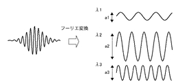
したがって、白色干渉信号(=インターフェログラム)をフーリエ変換して得られる情報は、干渉計の分光分布特性を示す情報を含む。これを図4、5の概念図を参照して更に具体的に説明する。図4の左側には、白色干渉信号が示されている。図4の右側には、該白色干渉信号をフーリエ変換した際の波長λ1、λ2、λ3の成分が示されている。振幅a1、a2、a3は、白色干渉信号をフーリエ変換して得られる結果の実部と虚部から算出される。即ち、振幅a1、a2、a3は、波長λ1、λ2、λ3に対応する周波数f1、f2、f3における振幅の大きさに比例する。 Therefore, the information obtained by Fourier transforming the white light interference signal (= interferogram) includes information indicating the spectral distribution characteristics of the interferometer. This will be described more specifically with reference to the conceptual diagrams of FIGS. The white interference signal is shown on the left side of FIG. The right side of FIG. 4 shows components of wavelengths λ1, λ2, and λ3 when the white interference signal is Fourier-transformed. The amplitudes a1, a2, and a3 are calculated from the real part and the imaginary part of the result obtained by Fourier transforming the white light interference signal. That is, the amplitudes a1, a2, and a3 are proportional to the amplitudes at the frequencies f1, f2, and f3 corresponding to the wavelengths λ1, λ2, and λ3.
図5には、白色干渉信号をフーリエ変換して得られた結果の振幅分布が示されている。周波数f1、f2、f3は、図4の波長λ1、λ2、λ3にそれぞれ対応し、周波数f1、f2、f3における振幅は、図4の振幅a1、a2、a3に対応する。図4において、波長λ1、λ2、λ3の成分の位相は、白色干渉信号をフーリエ変換して得られる結果の実部と虚部から算出される。 FIG. 5 shows an amplitude distribution obtained as a result of Fourier transform of the white light interference signal. The frequencies f1, f2, and f3 correspond to the wavelengths λ1, λ2, and λ3 in FIG. 4, respectively, and the amplitudes at the frequencies f1, f2, and f3 correspond to the amplitudes a1, a2, and a3 in FIG. In FIG. 4, the phases of the components of wavelengths λ1, λ2, and λ3 are calculated from the real part and the imaginary part of the result obtained by Fourier transforming the white light interference signal.
白色干渉信号をフーリエ変換した振幅の分布が凸形状であることは、周波数に応じて振幅が異なること、即ち、白色からずれた分光分布特性を有する干渉計によって白色干渉信号が検出されたことを意味する。 The fact that the amplitude distribution obtained by Fourier transform of the white interference signal has a convex shape means that the amplitude varies depending on the frequency, that is, that the white interference signal is detected by an interferometer having a spectral distribution characteristic deviated from white. means.
図4の左側に示された白色干渉信号の位相は、該白色干渉信号をフーリエ変換した結果の位相に対応し、振幅とは無関係である。一方、白色干渉信号の包絡線の形状は、白色干渉信号をフーリエ変換した結果の振幅に対応し、位相とは無関係である。 The phase of the white interference signal shown on the left side of FIG. 4 corresponds to the phase resulting from Fourier transform of the white interference signal, and is independent of the amplitude. On the other hand, the shape of the envelope of the white light interference signal corresponds to the amplitude of the result of Fourier transform of the white light interference signal and is independent of the phase.
そこで、この実施形態では、フーリエ変換した結果の位相はそのままとする一方で、振幅を周波数に対して一定の値となるように整形し、その後、逆フーリエ変換することで、高コントラストの白色干渉信号を得る。 Therefore, in this embodiment, while maintaining the phase as a result of the Fourier transformation, the amplitude is shaped so as to be a constant value with respect to the frequency, and then subjected to inverse Fourier transformation to thereby obtain high contrast white interference. Get a signal.
以下では、より厳密に表現するために、「白色」という用語を使用せずに、「広帯域光」という用語を使用する。その理由は、例えば、青色を使用しない波長領域(例えば、500nm〜800nm)の広帯域光を使用しても本発明による効果が得られるからである。また、広帯域光は、コンピュータによる信号処理により分離可能な複数の波長(または周波数)を含む光であると定義することができる。 In the following, for the sake of more precise expression, the term “broadband light” is used without using the term “white”. The reason is that, for example, the effect of the present invention can be obtained even when broadband light in a wavelength region (for example, 500 nm to 800 nm) that does not use blue is used. Broadband light can be defined as light including a plurality of wavelengths (or frequencies) that can be separated by signal processing by a computer.
図1は、本発明の好適な実施形態の形状測定装置の概略構成を示す図である。本発明の好適な実施形態の形状測定装置200は、干渉計10と、干渉計10から出力される信号に基づいて非計測面の形状を示す情報を発生するコンピュータ100とを備える。干渉計10は、被測定面からの測定光と参照面からの参照光とによって形成される干渉光を該測定光または該参照光の光路長を変更しながら光電変換素子(典型的には、光電変換素子が二次元状に配列されたイメージセンサ)で検知する。ここで、測定光および参照光は、広帯域光から生成され、測定光は被測定面で反射された後に参照光と干渉して干渉光を形成する。なお、二次元状に配列されたイメージセンサを光電変換素子として使う場合には、被測定面を参照面に対して相対的に傾けて、測定光と参照光の波面に角度差を与えることで、傾けた方向に各光電変換素子に入射する測定光の光路長を互いに異ならせることができる。そのように構成すれば、測定光または参照光の光路長を変更しながらイメージセンサで干渉光を測定する必要がなくなる。干渉計10としては、例えば、図6、図7に例示されるようなミラウ干渉計が好適である。以下では、説明の具体化のために干渉計10が図6、7に例示された干渉計であるものとして記述するが、干渉計10として他の種々の干渉計を使用することができることに留意されたい。
FIG. 1 is a diagram showing a schematic configuration of a shape measuring apparatus according to a preferred embodiment of the present invention. A
コンピュータ100は、干渉信号取得工程110、フーリエ変換工程120、整形工程130、逆フーリエ変換工程140、形状決定工程150を実施することができるように構成されている。典型的には、コンピュータ100は、干渉信号取得工程110、フーリエ変換工程120、整形工程130、逆フーリエ変換工程140、形状決定工程150に対応するプログラム(ソフトウエア)がインストールされることによって特徴づけられうる。他の観点で表現すれば、コンピュータ100は、干渉信号取得手段、フーリエ変換手段、整形手段、逆フーリエ手段、形状決定手段を備える。干渉信号取得手段、フーリエ変換手段、整形手段、逆フーリエ手段、形状決定手段によって、それぞれ干渉信号取得工程110、フーリエ変換工程120、整形工程130、逆フーリエ変換工程140、形状決定工程150が実行される。
The
図10は、広帯域光を用いて得られる干渉信号の一例を示す。なお、この例は、シミュレーションによって求めたものである。ここでは、図6、7に示されるミラウ干渉計を干渉計10として用いることを想定し、対物レンズ610を駆動させることで、光路長を変更するモデルで求めた。
FIG. 10 shows an example of an interference signal obtained using broadband light. This example is obtained by simulation. Here, assuming that the Mirau interferometer shown in FIGS. 6 and 7 is used as the
シミュレーションにおいて、使用する広帯域光の波長は、中心波長が550nmとし、光の強度分布は、ガウス分布(6σ=300nm)とした。また、広帯域光は、被測定面620に対してほぼ垂直に入射するものとした。また、波長のピッチを10nmとした。また、被測定面620および内部参照鏡612における反射率は、各波長で1.5とした。駆動素子(ピエゾ素子)による対物レンズ610の駆動のピッチを20nmとした。
In the simulation, the wavelength of the broadband light to be used has a center wavelength of 550 nm, and the light intensity distribution is a Gaussian distribution (6σ = 300 nm). The broadband light is incident on the surface to be measured 620 substantially perpendicularly. The wavelength pitch was 10 nm. Further, the reflectivity of the
このような広帯域光を用いて得られる図10に例示される干渉信号(第1干渉信号)をフーリエ変換した振幅の分布が図14に示されている。図14の右側には拡大図が示されている。図14において、分布の形状はガウス分布であり、光源の分光分布を反映していることが判る。干渉信号取得工程110では、コンピュータ100は、図10に例示されるような干渉信号(第1干渉信号)を干渉計10から取得する。フーリエ変換工程120では、コンピュータ100は、干渉信号取得工程110で取得した干渉信号をフーリエ変換して、位相分布と、図14に例示されるような振幅分布とを得る。
FIG. 14 shows an amplitude distribution obtained by Fourier-transforming the interference signal (first interference signal) illustrated in FIG. 10 obtained using such broadband light. An enlarged view is shown on the right side of FIG. In FIG. 14, it can be seen that the shape of the distribution is a Gaussian distribution and reflects the spectral distribution of the light source. In the interference
整形工程130では、コンピュータ100は、フーリエ変換工程120でフーリエ変換して得られた振幅分布を整形する。この整形は、図15に例示されるように、平坦部を有する振幅分布が形成されるように、または、平坦部が拡大された振幅分布が形成されるようになされうる。ここで、平坦部の両端において微分不連続にならないように整形がなされることが好ましい。
In the shaping step 130, the
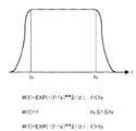
整形について、図2、3を参照しながら、より具体的に説明する。図2、図3は、整形後の振幅分布を例示している。図3は、図2における周波数fが正の部分を拡大したものである。 The shaping will be described more specifically with reference to FIGS. 2 and 3 illustrate the amplitude distribution after shaping. FIG. 3 is an enlarged view of a portion where the frequency f in FIG. 2 is positive.
整形工程130では、振幅分布が例えば次のような分布関数Wに従うように整形される。これは、各周波数における振幅の値を分布関数Wにおける振幅の値に一致するように変更すること、或いは、各周波数における振幅の値を分布関数Wにおける振幅の値で置き換えることを意味する。なお、フーリエ変換工程120でフーリエ変換して得られた位相分布については、整形工程130では変更(操作)しない。
In the shaping step 130, the amplitude distribution is shaped so as to follow the following distribution function W, for example. This means that the amplitude value at each frequency is changed to match the amplitude value at the distribution function W, or the amplitude value at each frequency is replaced with the amplitude value at the distribution function W. Note that the phase distribution obtained by Fourier transform in the
W(f)=EXP(−(f−fs)2/σ) : f<fs
W(f)=1 : fs≦f≦fe
W(f)=EXP(−(f−fe)2/σ) : f>fs
σは、ガウス関数の収束する速さを規定するものであり、ここでは、周波数のピッチの5倍の値とした。
W (f) = EXP (− (f−fs) 2 / σ ): f <fs
W (f) = 1: fs ≦ f ≦ fe
W (f) = EXP (− (f−fe) 2 / σ ): f> fs
σ prescribes the convergence speed of the Gaussian function, and here it is a value that is five times the frequency pitch.
分布関数Wの周波数fsと周波feの決定方法については後述する。 A method for determining the frequency fs and the frequency fe of the distribution function W will be described later.
逆フーリエ変換工程140では、コンピュータ100は、整形工程130で整形された振幅分布における振幅およびフーリエ変換工程120で得られた位相分布における位相を逆フーリエ変換する。これにより、図11に例示するような干渉信号(第2干渉信号)が得られる。図10(処理前)と図11(処理後)とを比較すれば明らかなように、コンピュータ100による信号処理によって干渉信号が高コントラスト化されている。
In the inverse
形状決定工程150では、コンピュータ100は、逆フーリエ変換によって得られた干渉信号に基づいて被測定面620の3次元形状を決定する。
In the
以下、コンピュータ100による高コントラスト化の効果を説明する。図12、図13は、図10(処理前)、図11(処理後)を信号の最大値が1となるようにに正規化した結果を示している。
Hereinafter, the effect of increasing the contrast by the
ここで、「コヒーレンス長」として、図8に示したように最大強度の20%以上の振幅を有する部分の横軸(垂直方向位置)の長さと定義して、図12、13を計測すると、それぞれ約3.6μm、2.6μmとなる。つまり、約30%分(1−2.6/3.6)だけコヒーレンス長が短くなっている。 Here, as “coherence length”, as shown in FIG. 8, it is defined as the length of the horizontal axis (vertical position) of the portion having the amplitude of 20% or more of the maximum intensity, and FIGS. These are about 3.6 μm and 2.6 μm, respectively. That is, the coherence length is shortened by about 30% (1-2.6 / 3.6).
高コントラスト化した広帯域光を用いた干渉信号(第2干渉信号)に基づいて形状決定工程150で被測定面の形状を決定する方法としては、前述のFDA法、位相シフト法やフーリエ変換法を使用することができる。
As a method of determining the shape of the surface to be measured in the
次に、振幅を整形するための分布関数Wの平坦部の両端の周波数fs、feを決定する方法について説明する。 Next, a method for determining the frequencies fs and fe at both ends of the flat portion of the distribution function W for shaping the amplitude will be described.
広帯域光を用いた干渉信号をフーリエ変換して得られる図5または図14に例示した振幅分布における凸形状部分の情報を十分に利用するように、分布関数Wの平坦部の両端の周波数fs、feを設定することが高コントラスト信号を得るために重要である。一方で、分布関数Wの平坦部を広く取り過ぎて測定精度を低下させることは避けるべきである。凸形状部分以外の信号を使用することは、位相情報がない部分の情報を追加することにより、測定精度を低下させる原因になる。 The frequency fs at both ends of the flat part of the distribution function W so that the information of the convex part in the amplitude distribution illustrated in FIG. 5 or FIG. 14 obtained by Fourier transforming the interference signal using the broadband light is sufficiently utilized. Setting fe is important for obtaining a high contrast signal. On the other hand, it should be avoided that the flat portion of the distribution function W is made too wide to reduce the measurement accuracy. The use of signals other than the convex portion causes a decrease in measurement accuracy by adding information of a portion without phase information.
そこで、広帯域光を用いた干渉信号をフーリエ変換して得られる位相分布における位相変化の度合いに基づいて周波数fs、feを設定することが好ましい。白色干渉の原理から、各波長における位相は、理想的な場合には、波長が変化すると徐々に位相も変化する。前述のFDAはこの現象を使用したものである。そこで、情報として信頼性が高い周波数の位相は徐々に変化するものと考え、位相変化の線形性が高い周波数領域の両端の周波数を周波数fs、feと設定することが好ましい。つまり、位相分布を示す曲線の線形性が基準値より高い周波数領域において平坦化された振幅分布が形成されるように、振幅分布の整形がなされることが好ましい。 Therefore, it is preferable to set the frequencies fs and fe based on the degree of phase change in the phase distribution obtained by Fourier transforming the interference signal using broadband light. From the principle of white interference, the phase at each wavelength is ideally changed gradually as the wavelength changes. The aforementioned FDA uses this phenomenon. Therefore, it is considered that the phase of the frequency with high reliability as information changes gradually, and it is preferable to set the frequencies at both ends of the frequency region where the linearity of the phase change is high as the frequencies fs and fe. That is, it is preferable that the amplitude distribution is shaped so that a flattened amplitude distribution is formed in a frequency region where the linearity of the curve indicating the phase distribution is higher than the reference value.
線形性が高い領域と低い領域との区別は、例えば、線形性が基準値以上であるか否かによって決定されうる。具体的には、位相を周波数で微分した値が基準値より低い領域は線形性が高い領域、該基準値より高い領域は線形性が低い領域と判断することができる。 The distinction between a region with high linearity and a region with low linearity can be determined, for example, by whether or not the linearity is equal to or higher than a reference value. Specifically, it can be determined that the region where the value obtained by differentiating the phase with respect to the frequency is lower than the reference value is a region having high linearity, and the region having a value higher than the reference value is a region having low linearity.
図16は、図10に例示される干渉信号をフーリエ変換して得られる振幅および位相の分布を示している。図16から明らかなように、フーリエ変換後の振幅の値が小さい領域でもフーリエ変換後の位相がほぼ線形である。そこで、位相の値がほぼ線形に変化している領域の両端を周波数fs、feとする分布関数Wを設定することが好ましい。 FIG. 16 shows the amplitude and phase distribution obtained by Fourier transform of the interference signal illustrated in FIG. As is apparent from FIG. 16, the phase after the Fourier transform is almost linear even in the region where the amplitude value after the Fourier transform is small. Therefore, it is preferable to set the distribution function W having the frequencies fs and fe at both ends of the region where the phase value changes almost linearly.
なお、ここまでは干渉方式としてミラウ型に関して説明をしてきたが、本発明の適用はこれに限定されず、本発明は、例えば、マイケルソン型やリニーク型のような他の干渉方式にも適用することができる。 Although the description has been made so far with respect to the Mirau type as an interference method, the application of the present invention is not limited to this, and the present invention is also applicable to other interference methods such as a Michelson type and a linique type, for example. can do.
この実施形態によれば、例えば、光源、光学系、光電変換素子の分光特性の影響を受けることなく、広帯域光を用いて高コントラストな干渉信号を得ることができる。 According to this embodiment, for example, a high-contrast interference signal can be obtained using broadband light without being affected by the spectral characteristics of the light source, the optical system, and the photoelectric conversion element.
[リソグラフィーへの応用例]
本発明は、複数の透明膜(多層膜)で構成される縦構造(積層構造)における特定の面を計測することにも適している。
[Application examples for lithography]
The present invention is also suitable for measuring a specific surface in a vertical structure (laminated structure) composed of a plurality of transparent films (multilayer films).
図17は、半導体デバイスの製造におけるリソグラフィーで使用される構造体、具体的には、シリコンウエハの上にレジストが塗布された構造体を例示的に示している。このレジストの表面形状を計測するために500nm程度の波長の光を使用する場合を考える。現在のリソグラフィーで使用されているレジストは、例えば365nm、248nm、193nmの波長を有する露光光には感光するが、500nmの波長の測定用の光に対しては透明状態である。したがって、図17に模式的に示すように、光線1のごとくレジスト表面で反射する光だけでなく、光線2のごとくレジスト裏面とシリコン基板との境界面から反射する光も発生する。よって、図示しない参照光を含めて合計で3つの光によって干渉像が形成され、これが計測誤差を生じさせ、正しくレジストの表面形状を計測することができない。
FIG. 17 exemplarily shows a structure used in lithography in manufacturing a semiconductor device, specifically, a structure in which a resist is applied on a silicon wafer. Consider a case where light having a wavelength of about 500 nm is used to measure the surface shape of the resist. The resist used in the current lithography is sensitive to exposure light having wavelengths of, for example, 365 nm, 248 nm, and 193 nm, but is transparent to measurement light having a wavelength of 500 nm. Accordingly, as schematically shown in FIG. 17, not only light reflected by the resist surface like the
この対応策として、Zygo社から”Top Slice”または”Tops Surface”と呼ぶ機能で製品に適用され効果が確認されている技術がある。この技術は、米国特許出願第2005/0078318号に開示されている。 As a countermeasure, there is a technique that has been applied to a product by a function called “Top Slice” or “Top Surface” from Zygo and its effect has been confirmed. This technique is disclosed in US Patent Application No. 2005/0078318.
本発明を”Top Slice”に適用することにより、レジスト表面の検出精度を更に向上させることができる。 By applying the present invention to “Top Slice”, the detection accuracy of the resist surface can be further improved.
まず、”Top Slice”の機能を説明する。図18Aは、広帯域光を用いた干渉信号を示している。図18Aの横軸の左側がシリコン基板方向、右側がレジスト表面方向である。干渉信号のピーク404はレジスト裏面とシリコン基板との境界面に対応し、干渉信号のピーク402は、レジスト表面に対応する。言い換えれば、図18Aの信号は、2つの干渉信号で構成されている。レジスト厚が薄くなり、レジスト裏面とシリコン基板との境界面に対応する干渉信号がレジスト表面に対応する干渉信号に影響を及ぼすと、検出精度が劣化させる可能性がある。
First, the function of “Top Slice” will be described. FIG. 18A shows an interference signal using broadband light. The left side of the horizontal axis in FIG. 18A is the silicon substrate direction, and the right side is the resist surface direction. The
そこで、”Top Slice”では、図18Bに示されるように、テンプレートとして、干渉信号の右側のピーク402(レジスト表面に対応するピーク)に対応する波形315を使用する。そして、そのテンプレートと図18Aの信号に対してマッチング処理を行い、マッチ度(図18C)に基づいてレジスト表面(図18Cの最も右側のピークの位置)を検出する。
Therefore, in “Top Slice”, as shown in FIG. 18B, a
このように、この技術は、積層構造における最表面を検出するため、”Top Slice”または”Tops Surface”と呼ばれている。レジスト裏面とシリコン基板との境界面を検出したい場合には、設定を変更して、図18C最も左側のピークの位置を検出すればよい。 As described above, this technique is called “Top Slice” or “Top Surface” in order to detect the outermost surface in the laminated structure. If it is desired to detect the boundary surface between the resist back surface and the silicon substrate, the setting may be changed to detect the position of the leftmost peak in FIG. 18C.
このように、”Top Slice”では、複数の面から反射した光による干渉信号に基づいて最表面を検出することを可能としている。 As described above, in “Top Slice”, it is possible to detect the outermost surface based on the interference signal due to the light reflected from a plurality of surfaces.
この”Top Slice”を使用しても、レジスト厚が更に薄くなり、レジスト裏面とシリコン基板との境界面に対応する干渉信号がレジスト表面に対応する干渉信号に影響を及ぼすと、検出精度が劣化する可能性がある。 Even if this “Top Slice” is used, if the resist thickness is further reduced and the interference signal corresponding to the boundary surface between the resist back surface and the silicon substrate affects the interference signal corresponding to the resist surface, the detection accuracy deteriorates. there's a possibility that.
そのような場合に、本発明を適用して信号を高コントラスト化することで、検出精度を向上させることができる。具体的には、コンピュータ100は、形状決定工程150において、逆フーリエ変換によって生成された干渉信号(第2干渉信号)の包絡線が有する複数のピークから1つのピークを選択し、その選択したピークに基づいて被測定面の形状を決定する。
In such a case, the detection accuracy can be improved by applying the present invention to increase the contrast of the signal. Specifically, the
実際のリソグラフィーにおいては、レジストの上に反射防止層やキャップ層と呼ばれる層が塗布され、それらの層の屈折率はほぼレジストと同じである。そこで、それらの層が塗布された積層構造においても、本発明を適用すると、その積層構造の表面を高精度で計測することができる。 In actual lithography, a layer called an antireflection layer or a cap layer is applied on a resist, and the refractive index of these layers is almost the same as that of the resist. Therefore, even in a laminated structure in which these layers are applied, the surface of the laminated structure can be measured with high accuracy by applying the present invention.
[第1実施例]
本発明は、被測定面に対してほぼ垂直に広帯域光を入射させる構成に限定されず、図19に例示するように、被測定面に対して斜めに広帯域光を入射させる干渉系にも適用可能である。
[First embodiment]
The present invention is not limited to the configuration in which broadband light is incident substantially perpendicularly to the surface to be measured, and is also applied to an interference system in which broadband light is incident obliquely with respect to the surface to be measured, as illustrated in FIG. Is possible.
図20は、図19に示される構成の下でシミュレーションにより求めた干渉信号を示している。このシミュレーションで使用した広帯域光の波長は400nm〜700nm(ピッチ10nm)、入射角度(θin)は75度である。計測対象物は、レジストとした。ここで、レジストの厚さを20ミクロン以上として、レジストの裏面からの反射を分離することができるようにした。参照面はSiO2とした。ピエゾによる参照ミラーの駆動のピッチは77.2nmとした。 FIG. 20 shows an interference signal obtained by simulation under the configuration shown in FIG. The wavelength of the broadband light used in this simulation is 400 nm to 700 nm (pitch 10 nm), and the incident angle (θin) is 75 degrees. The measurement object was a resist. Here, the thickness of the resist is set to 20 microns or more so that reflection from the back surface of the resist can be separated. Reference plane was SiO 2. The driving pitch of the reference mirror by the piezo was 77.2 nm.
光源としては、図9に示される分光分布の白色LEDと呼ばれる光源を使用した。 As the light source, a light source called a white LED having a spectral distribution shown in FIG. 9 was used.
この広帯域光を用いた干渉信号をフーリエ変換した振幅分布を図24に示す。図24の右側は左側の拡大図である。分布の形状は、図9の形状を反転した形状であり、光源の分光分布を反映していることが判る(反転しているのは、周波数の共役な方の分布を拡大したため)。 FIG. 24 shows an amplitude distribution obtained by Fourier transforming the interference signal using the broadband light. The right side of FIG. 24 is an enlarged view of the left side. The shape of the distribution is a shape obtained by reversing the shape of FIG. 9 and reflects the spectral distribution of the light source (the reason for the reversal is that the frequency-conjugated distribution is enlarged).
図25に例示するような分布関数Wを定義し、これを使用して逆フーリエ変換を行った結果を図21に示す。図20、21の信号をその最大値で正規化した信号を図22、図23にそれぞれ示す。コヒーレンス長を前述と同ように最大強度の20%の幅の信号の横軸の長さと定義して、図22、23を計測するとそれぞれ約13.9μm、5.8μmとなる。つまり、本発明の適用により、コヒーレンス長が約40%(5.8/13.9)になっている。 FIG. 21 shows the result of defining the distribution function W as exemplified in FIG. 25 and performing inverse Fourier transform using this. Signals obtained by normalizing the signals of FIGS. 20 and 21 with their maximum values are shown in FIGS. 22 and 23, respectively. When the coherence length is defined as the length of the horizontal axis of a signal having a width of 20% of the maximum intensity as described above, the measurement results in FIGS. 22 and 23 are about 13.9 μm and 5.8 μm, respectively. That is, the coherence length is about 40% (5.8 / 13.9) by applying the present invention.
[第2実施例]
斜入射でかつ複数の反射面を有する場合(例えば、第1実施例における構成で得られる干渉信号を「リソグラフィーへの応用例」に示す方法で処理する場合)においても本発明を適用することで高精度な計測が可能となる。
[Second Embodiment]
By applying the present invention even in the case of oblique incidence and having a plurality of reflecting surfaces (for example, when the interference signal obtained by the configuration in the first embodiment is processed by the method shown in “Application Examples to Lithography”), High-precision measurement is possible.
上記のような方法で干渉信号をフーリエ変換して得られた振幅分布を図3に示す分布関数Wに従うように整形しても、複数の透明膜(多層膜)で構成される縦構造(積層構造)によっては、高精度な検出精度が得られない可能性がある。これは、積層構造によっては反射位相(反射光の位相)が異常になる周波数が存在することに起因する。以下に、反射位相が異常な周波数とは何かの説明をする。 Even if the amplitude distribution obtained by Fourier-transforming the interference signal by the above method is shaped so as to follow the distribution function W shown in FIG. 3, a vertical structure (laminated layer) composed of a plurality of transparent films (multilayer films) Depending on the structure, there is a possibility that high-precision detection accuracy cannot be obtained. This is due to the presence of a frequency at which the reflection phase (the phase of the reflected light) becomes abnormal depending on the laminated structure. In the following, what is a frequency with an abnormal reflection phase will be described.
図27は、240nm厚のレジスト厚、78nm厚のBARK、180nm厚のSiO2をCu基板の上に積層した構造の一例を示す図である。屈折率は、レジストが1.54、BARKが1.53、SiO2が1.46、Cu基板が実部0.38、虚部2.9である。そして、この積層構造のS偏光、P偏光の波長に対する反射強度を図28に、反射位相を図29に示した。図28の縦軸は反射強度(1が反射率100%)、横軸は波長(μm)である。図29の縦軸は位相(ラジアン)、横軸は波長(μm)である。波長領域が0.4μm(400nm)から0.8μm(800nm)の範囲であるのは、図9に示した波長領域(400nmから800nm)の白色LED光源で図19に示した干渉計を用いて取得した干渉信号の例を以下に示すためである。 FIG. 27 is a view showing an example of a structure in which a resist thickness of 240 nm, a BARK thickness of 78 nm, and a SiO 2 thickness of 180 nm are stacked on a Cu substrate. The refractive indexes are 1.54 for resist, 1.53 for BARK, 1.46 for SiO 2 , real part 0.38 and imaginary part 2.9 for Cu substrate. FIG. 28 shows the reflection intensity with respect to the wavelengths of the S-polarized light and the P-polarized light of this laminated structure, and FIG. 29 shows the reflection phase. In FIG. 28, the vertical axis represents the reflection intensity (1 is the reflectance of 100%), and the horizontal axis represents the wavelength (μm). In FIG. 29, the vertical axis represents phase (radian), and the horizontal axis represents wavelength (μm). The wavelength region is in the range of 0.4 μm (400 nm) to 0.8 μm (800 nm) using the white LED light source in the wavelength region (400 nm to 800 nm) shown in FIG. 9 using the interferometer shown in FIG. This is because an example of the acquired interference signal is shown below.
図28に示した例において、S偏光の反射強度は波長500nm近傍で急激に低下し、P偏光の反射強度は波長650nm近傍で急激に低下している。一方、図29に示した例において、S偏光の反射位相は波長500nm近傍で急激に変化し、P偏光の反射位相は波長650nm近傍で急激に変化している。S偏光の600nm近傍の位相は、3ラジアンから−3ラジアンになっているので位相変化はない。このように、反射位相が急激に変化している波長近傍では、反射強度も急激に低下する。ここで、反射強度および反射位相が急激に変化する波長を反射位相が異常波長(異常周波数)と定義する。 In the example shown in FIG. 28, the reflection intensity of S-polarized light sharply decreases near the wavelength of 500 nm, and the reflection intensity of P-polarized light decreases rapidly near the wavelength of 650 nm. On the other hand, in the example shown in FIG. 29, the reflection phase of S-polarized light changes abruptly in the vicinity of a wavelength of 500 nm, and the reflection phase of P-polarized light changes abruptly in the vicinity of a wavelength of 650 nm. Since the phase of S-polarized light in the vicinity of 600 nm is changed from 3 radians to -3 radians, there is no phase change. Thus, in the vicinity of the wavelength where the reflection phase changes rapidly, the reflection intensity also decreases rapidly. Here, a wavelength at which the reflection intensity and the reflection phase change rapidly is defined as an abnormal wavelength (abnormal frequency) of the reflection phase.
前述のように、干渉信号は、白色干渉の原理から理解されるように、波長の変化に伴って位相が徐々に変化することが理想である。しかし、図27のような積層構造での干渉信号では、図28および図29に例示した反射位相が異常な異常波長(異常周波数)で反射位相が急激に変化し、理想的な干渉信号でなくなる。このことは、白色干渉信号が、複数の波長(周波数)の干渉信号の総和であることからも明らかである。 As described above, it is ideal that the phase of the interference signal gradually changes as the wavelength changes, as understood from the principle of white light interference. However, in the case of an interference signal having a laminated structure as shown in FIG. 27, the reflection phase abruptly changes at an abnormal wavelength (abnormal frequency) in which the reflection phase illustrated in FIGS. . This is apparent from the fact that the white interference signal is the sum of interference signals of a plurality of wavelengths (frequencies).
このように、積層構造によっては、反射位相が異常になる周波数が存在する干渉信号に対して図1を参照して説明した処理を行うことで、反射位相が異常になる周波数の成分が強調されうる。その結果、レジスト表面に対応する干渉信号に悪影響を及ぼしてしまい、高い検出精度が得られない可能性がある。 As described above, depending on the laminated structure, by performing the processing described with reference to FIG. 1 on the interference signal having the frequency at which the reflection phase becomes abnormal, the frequency component at which the reflection phase becomes abnormal is emphasized. sell. As a result, the interference signal corresponding to the resist surface is adversely affected, and high detection accuracy may not be obtained.
[第3実施例]
本発明の第3実施例について詳細に説明する。第3実施例の特徴は、図1を参照して説明した振幅分布の整形工程130にある。図3を参照して説明例では、位相分布の線形成の良い周波数領域を整形対象の周波数領域とし、その整形対象の周波数領域の振幅を平坦化する。
[Third embodiment]
The third embodiment of the present invention will be described in detail. The feature of the third embodiment resides in the amplitude distribution shaping step 130 described with reference to FIG. In the description example with reference to FIG. 3, a frequency region with good phase distribution line formation is set as a frequency region to be shaped, and the amplitude of the frequency region to be shaped is flattened.
図30は、第3実施例における整形工程130の手順を示す図である。第3実施例における整形工程130では、まず、工程3010において、予め定められた値以上の振幅が存在する周波数領域を整形対象の周波数領域とする。次に、工程3020において、位相分布から位相変化を算出する。次いで、工程3030において、整形対象の周波数領域のうち位相変化が異常な異常周波数領域を判断する。次いで、工程3040において、位相変化が異常であると判断した異常周波数領域の振幅が他の周波数領域の振幅に比べて小さくなるように、当該整形対象の周波数領域における振幅分布を整形する。以下において、工程3010から工程3040のより具体的な例を説明する。
FIG. 30 is a diagram showing the procedure of the shaping step 130 in the third embodiment. In the shaping step 130 in the third embodiment, first, in
スペクトル情報が存在する領域の両端には、反射位相の異常な異常周波数が含まれる場合がある。よって、位相分布を用いると整形対象の周波数領域の決定を誤ってしまう可能性がある。そこで、工程3010では、振幅分布に基づいて整形対象の周波数領域を決定する。ここで、整形対象の周波数領域は、フーリエ変換した振幅分布の最大値に対する基準の割合以上の振幅を有する周波数領域とすることができる。或いは、整形対象の周波数領域は、フーリエ変換した振幅分布の全周波数領域におけるスペクトル強度の中央値より大きな強度の周波数領域としても良い。或いは、整形対象の周波数領域は、光源の波長領域に対応する周波数領域としても良い。
There are cases where abnormal frequencies with an abnormal reflection phase are included at both ends of the region where the spectral information exists. Therefore, when the phase distribution is used, there is a possibility that the frequency domain to be shaped is erroneously determined. Therefore, in
以下では、フーリエ変換した振幅分布の全周波数領域におけるスペクトル強度の中央値より大きな強度の周波数領域を整形対象の周波数領域とする例を示す。 In the following, an example is shown in which a frequency region having an intensity greater than the median spectral intensity in the entire frequency region of the Fourier-transformed amplitude distribution is used as a shaping target frequency region.
図31は、図19に示した構成の下でシミュレーションにより求めた干渉信号である。計算条件として、光源は図9に示した白色LED光源(波長400nm〜800nm、ピッチ10nm)、入射角(θin)は75度とした。また、計測対象物は図27に示した積層構造の厚さ240nmのレジストとした。参照面はSiO2とした。ピエゾによる参照面の駆動ピッチは77.2nmとし、計測対象物に近づける方向に該参照面を駆動した。図31の横軸はピエゾ駆動位置に相当し、各位置の間隔が77.2nmで、総数数は512点である。縦軸は干渉信号の強度である。参照面とレジスト表面でそれぞれ反射する光の光路長がそろう位置は312点としている。
FIG. 31 shows an interference signal obtained by simulation under the configuration shown in FIG. As calculation conditions, the light source was a white LED light source (
図31に示す干渉信号をフーリエ変換した結果を図32、図33に示す。図32は、第1実施例において参照した図24の拡大図(フーリエ変換した振幅分布の拡大図)に相当する。ここでは、振幅分布における振幅の最大値で規格化した。縦軸は規格化後のスペクトル強度、横軸は周波数である。そして、全周波数領域の規格化後のスペクトル強度の中央値は0.1であったので、規格化後のスペクトル値が0.1以上の周波数領域を整形対象の周波数領域とした。この干渉信号では、460から488の周波数領域と、それに共役な周波数領域が整形対象の周波数領域である。 The result of Fourier transforming the interference signal shown in FIG. 31 is shown in FIGS. FIG. 32 corresponds to the enlarged view of FIG. 24 (enlarged view of the amplitude distribution obtained by Fourier transform) referred to in the first embodiment. Here, normalization was performed with the maximum value of the amplitude in the amplitude distribution. The vertical axis represents the spectral intensity after normalization, and the horizontal axis represents the frequency. Since the median value of the spectrum intensity after normalization in all frequency regions was 0.1, the frequency region having a spectrum value after normalization of 0.1 or more was determined as the frequency region to be shaped. In this interference signal, a frequency region from 460 to 488 and a frequency region conjugate to the frequency region are frequency regions to be shaped.
ここでの全周波数領域とは、光源の波長スペクトルに設定されるものではなく、図31に示す干渉信号から決まるカットオフ周波数以下の周波数領域(直流成分は除く)である。 Here, the total frequency region is not set in the wavelength spectrum of the light source, but is a frequency region (excluding the DC component) below the cutoff frequency determined from the interference signal shown in FIG.
次に、工程3020について具体的に説明する。図33に、工程3010で決定した整形対象の周波数領域(460から488)における、フーリエ変換した位相分布を示す。縦軸はラジアン、横軸は周波数である。その位相分布を用いて、整形対象の周波数領域(460から488)の前後の周波数に対する位相変化(位相分布の傾き)を求める。その結果を図34に例示する。
Next, the
工程3030では、整形対象の周波数領域(460から488)において、工程3020で求めた位相変化(位相分布の傾き)の中央値を求める。この例では、中央値は2.7ラジアンである。そして、中央値からの差の絶対値が所定量以上の周波数を異常周波数とする。所定量は、図19に示した構成の干渉計に関して、予めシミュレーションの干渉信号から積層構造に最適な量を求めておく。
In
所定量は、例えば、標準偏差の0.1倍以上3.0倍以下の値とすることができる。 The predetermined amount can be, for example, a value not less than 0.1 times and not more than 3.0 times the standard deviation.
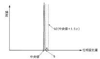
位相変化量の頻度分布は、図44Aに示すような一様分布、或いは、図44Bに示すような正規分布、或いは、図44Cに示すような二極化した分布となりうる。何れの図も横軸は位相変化量、縦軸はその頻度である。図44Aのような一様分布の場合、例えば、中央値より1.5倍のσ(σは、標準偏差)以上の差がある位相変化量を外れ値とみなすことができる。図44Aの例では、b1以下の位相変化量とb2以上の位相変化量が外れ値である。図44Bのような正規分布の場合、例えば、中央値より3.0倍のσ(σは、標準偏差)以上の差がある位相変化量を外れ値とみなすことができる。図44Bの例では、b1以下の位相変化量とb2以上の位相変化量が外れ値である。そして、外れ値とみなした位相変化量に対応する周波数を異常周波数とする。 The frequency distribution of the phase change amount can be a uniform distribution as shown in FIG. 44A, a normal distribution as shown in FIG. 44B, or a bipolar distribution as shown in FIG. 44C. In each figure, the horizontal axis represents the phase change amount, and the vertical axis represents the frequency. In the case of a uniform distribution as shown in FIG. 44A, for example, a phase change amount having a difference of σ (σ is a standard deviation) equal to or greater than 1.5 times the median value can be regarded as an outlier. In the example of FIG. 44A, a phase change amount of b1 or less and a phase change amount of b2 or more are outliers. In the case of a normal distribution as shown in FIG. 44B, for example, a phase change amount having a difference of σ (σ is a standard deviation) or more that is 3.0 times the median value can be regarded as an outlier. In the example of FIG. 44B, a phase change amount of b1 or less and a phase change amount of b2 or more are outliers. A frequency corresponding to the phase change amount regarded as an outlier is set as an abnormal frequency.
図44Cは、b以上の位相変化量に対応する周波数が異常周波数の場合を示している。また、bは、中央値以上であり、しかも、中央値に1.5倍のσ(σは標準偏差)を加算したb2以下の値である。二極化した分布の場合、前述のような正規分布や一様分布のように中央値からの差がσ(σは、標準偏差)のn倍以上を外れ値と決めることはできない。それは、計測物体により干渉信号は異なり、位相変化量の外れ値bの値が変化するからである。このような分布の場合、中央値よりn倍のσ(σは、標準偏差)以上の差がある位相変化量を外れ値とみなす。具体的には、実験的に、nを0.1以上3.0以下とすることができる。最も計測精度が良いnの値は、実験的に0.3である。 FIG. 44C shows a case where the frequency corresponding to the phase change amount equal to or greater than b is an abnormal frequency. In addition, b is equal to or greater than the median, and is equal to or less than b2 obtained by adding 1.5 times σ (σ is a standard deviation) to the median. In the case of a bipolar distribution, a difference from the median of n or more than σ (σ is a standard deviation) cannot be determined as an outlier as in the normal distribution or uniform distribution as described above. This is because the interference signal differs depending on the measurement object, and the outlier value b of the phase change amount changes. In the case of such a distribution, a phase change amount having a difference of σ (σ is a standard deviation) or more that is n times the median is regarded as an outlier. Specifically, n can be experimentally set to 0.1 or more and 3.0 or less. The value of n with the best measurement accuracy is experimentally 0.3.
図27に示すような積層構造を有する計測対象物の場合、所定量は、整形対象の周波数領域(460から488)の位相変化量の標準偏差の0.3倍である0.5ラジアンとすることができる。この所定量によると、2.2から3.2ラジアンの位相変化量は正常とみなし、それ以外は異常と判断される。その結果、整形対象の周波数領域(460から488)では、460〜462、468〜469、480〜481、486〜488の周波数が異常異常周波数とされる。 In the case of a measurement object having a laminated structure as shown in FIG. 27, the predetermined amount is 0.5 radians, which is 0.3 times the standard deviation of the phase change amount in the frequency region (460 to 488) to be shaped. be able to. According to this predetermined amount, the phase change amount of 2.2 to 3.2 radians is regarded as normal, and otherwise it is determined as abnormal. As a result, in the frequency region to be shaped (460 to 488), the frequencies of 460 to 462, 468 to 469, 480 to 481, and 486 to 488 are abnormal and abnormal frequencies.
最後に、工程3040では、整形対象の周波数領域(460から488)において、工程3030で判断した異常周波数領域の振幅を他の周波数領域(正常周波数領域)の振幅よりも小さくする。それに共役な周波数領域も同様に振幅を整形する。例えば、前述のように平坦部の両端において微分不連続にならないように、図35に示す分布関数Wに従うように振幅分布を整形する。或いは、異常周波数領域の振幅をゼロにし他の周波数の振幅を平坦にし、その振幅分布に平滑化処理を行っても良い。本実施例では、まず、460〜462、468〜469、480〜481、486〜488の周波数領域を異常周波数領域として、当該異常周波数領域の振幅をゼロにし、他の周波数領域を1とした。図36は整形後の振幅分布である。更に、この振幅分布に幅3の移動平均を行って最終的な整形後の振幅分布を得ることができる。図37は、最終的な整形後の振幅分布である。同様の操作を共役な周波数領域に行う。
Finally, in
ここまでは、レジスト厚が240nmを例に説明した。図38は、レジスト厚を100nmから300nmまで20nmピッチで変化させてシミュレーションにより求めた干渉信号に対して、第1、第3実施例に従って求められるレジストの表面位置の平均誤差量(nm)を示している。縦軸は平均誤差量(nm)である。第1実施例における平均誤差量が14nmであるのに対して、第3実施例における平均誤差量は8nm弱であり、45%の改善が認められる。 Up to this point, the resist thickness is 240 nm as an example. FIG. 38 shows the average error amount (nm) of the resist surface position obtained according to the first and third embodiments with respect to the interference signal obtained by simulation by changing the resist thickness from 100 nm to 300 nm at a 20 nm pitch. ing. The vertical axis represents the average error amount (nm). While the average error amount in the first embodiment is 14 nm, the average error amount in the third embodiment is slightly less than 8 nm, and an improvement of 45% is recognized.
以上のように、第3実施例によれば、異常周波数領域の振幅を正常周波数領域の振幅に比べ抑制することで、検出精度を向上させることができる。 As described above, according to the third embodiment, the detection accuracy can be improved by suppressing the amplitude in the abnormal frequency region as compared with the amplitude in the normal frequency region.
[第4実施例]
本発明の第4実施例について詳細に説明する。第3実施例では異常周波数領域の判断に位相分布を用いる。一方、第4実施例では、振幅分布に基づいて異常周波数領域を判断する。図28と図29を参照して説明したように、反射位相の変化が急激な周波数領域と反射強度の急激な低下とは相関を有するので、第4実施例では、位相分布を用いる代わりに振幅分布を用いる。
[Fourth embodiment]
The fourth embodiment of the present invention will be described in detail. In the third embodiment, the phase distribution is used to determine the abnormal frequency region. On the other hand, in the fourth embodiment, the abnormal frequency region is determined based on the amplitude distribution. As described with reference to FIG. 28 and FIG. 29, the frequency region where the change in the reflection phase is abrupt has a correlation with the sudden decrease in the reflection intensity. Therefore, in the fourth embodiment, the amplitude is used instead of using the phase distribution. Use the distribution.
図39は、第4実施例の手順を示している。第4実施例では、図39に示す手順を実行する前に計測対象物の干渉信号を取得し(図1の工程110)、その干渉信号のフーリエ変換を行う(図1の工程120)。その後、図39に示す手順を実行する。まず、工程3910では、透明膜で構成されていない基準プレート(例えば、オプティカルフラット、SiO2プレートなど)の干渉信号を図1の工程110と同じ干渉計で取得する。次に、工程3920では、基準プレートの干渉信号をフーリエ変換して振幅分布を算出し、その振幅分布を示すデータを保存する。その後、工程3930では、その振幅分布において、予め定められた値以上の振幅が存在する周波数領域を整形対象の周波数領域とする。
FIG. 39 shows the procedure of the fourth embodiment. In the fourth embodiment, before executing the procedure shown in FIG. 39, an interference signal of the measurement object is acquired (
工程3940では、計測対象物の振幅分布、および、基準プレートの振幅分布を規格化する。工程3950では、複数の周波数のそれぞれについて、基準プレートの干渉信号をフーリエ変換して得られる振幅に対する計測対象物の干渉信号をフーリエ変換して得られる振幅の割合を算出する。工程3960では、整形対象の周波数領域において、振幅の割合が所定値以下の周波数領域を異常周波数領域と判断する。最後に、工程3970では、異常周波数領域の振幅が整形対象の周波数領域の中の他の周波数領域の振幅に比べて小さくなるように整形対象の周波数器の周波数分布を整形する。
In
工程3910で使用する基準プレートとしては、反射強度の周波数特性が平坦であり、しかも、反射位相の急激な変化がないものを採用すべきである。 As a reference plate used in Step 3910, a plate having a flat frequency characteristic of reflection intensity and no sudden change in reflection phase should be adopted.
以下に各工程のより具体的な例を説明する。工程3910では、基準プレートをSiO2プレートとする。図1の工程110におけるものと同様の干渉計でシミュレーションにより求めた干渉信号を図40に示した。SiO2プレートの厚さは裏面からの反射光が干渉しないように十分に厚い(例えば、数mm)ものを使用し、屈折率は1.46とした。総点数は512点である。
A more specific example of each process will be described below. In step 3910, the reference plate is a SiO 2 plate. FIG. 40 shows an interference signal obtained by simulation with an interferometer similar to that in
工程3920では、工程3910で取得した干渉信号をフーリエ変換して振幅分布を算出し、その振幅分布を示すデータを保存する。図41は、図40のSiO2基準プレートの干渉信号をフーリエ変換して得られる振幅分布を規格化した結果を示す図である。
In
工程3930では、第3実施例の計測対象物の干渉信号(図31)において、460から488の周波数領域とそれに共役な周波数領域を整形対象の周波数領域として決定する。
In
工程3940では、第3実施例の計測対象物の干渉信号(図31)のフーリエ変換の振幅分布、および、工程3930で算出した基準プレートの干渉信号(図40)のフーリエ変換の振幅分布をそれぞれ規格化した。図32に、計測対象物の干渉信号をフーリエ変換して得られる振幅分布を規格化した分布(以下、規格化後の計測対象物の振幅分布とする)を示した。図42に、基準プレートの干渉信号をフーリエ変換して得られる振幅分布を規格化した分布(以下、規格化後の基準プレートの振幅分布とする)を示した。図42に示した周波数範囲は、図32と同様に整形対象の周波数領域(460から488)である。図42には、整形対象の周波数領域(460から488)で、規格化後の計測対象物についての振幅分布と規格化後の基準プレートについての振幅分布を示した。
In
工程3950では、工程3940で算出した規格化後の計測対象物の振幅分布と規格化後の基準プレートの振幅分布とに基づいて、周波数毎に、規格化後の基準プレートについての振幅に対する規格化後の計測対象物についての振幅割合を算出する。図43にその結果を示した。縦軸が割合、横軸が周波数である。
In
工程3960で使用する所定値は、計測対象物のシミュレーションの干渉信号の振幅分布と基準プレートのシミュレーションの干渉信号の振幅分布とに基づいて予め最適な値を求めておく。実験上、最適な値は、例えば、0以上1.0未満の値である。更に、実験的に、最適な値は、0.8が最も精度が良い。
The predetermined value used in the
第4実施例では、所定値を0.8とした。その結果、整形対象の周波数領域(460から488)では、460から462、468から469、480から481、486から488の周波数領域が異常周波数領域となった。 In the fourth embodiment, the predetermined value is 0.8. As a result, in the frequency region to be shaped (460 to 488), the frequency region of 460 to 462, 468 to 469, 480 to 481, and 486 to 488 became the abnormal frequency region.
工程3970は、第3実施例の工程3040と同様の操作を行った。なお、工程3910と工程3920は、光源の波長分布やセンサの分光感度が不変であれば一度だけ行い、その後は保存された基準プレートの振幅データを用いることができる。また、これら手順は、光源やセンサを変更した場合に行うようにする。
更に、計測対象物の干渉信号の取得と基準プレートの干渉信号の取得の順序は、逆であってもよい。また、図39の工程3920において、基準プレートの干渉信号をフーリエ変換し振幅分布を算出し保存する例を示したが、工程3940で規格化後の基準プレートの振幅分布を保存し用いてもよい。
Furthermore, the order of obtaining the interference signal of the measurement object and obtaining the interference signal of the reference plate may be reversed. Further, in
[第5実施例]
第3実施例と第4実施例では、位相分布から判断した異常周波数領域と振幅分布から判断した異常周波数領域が同じになる例を示したが、両者の間で異常周波数領域が異なる場合もある。
[Fifth embodiment]
In the third embodiment and the fourth embodiment, an example is shown in which the abnormal frequency region determined from the phase distribution and the abnormal frequency region determined from the amplitude distribution are the same, but the abnormal frequency region may be different between the two. .
その場合、まず、第3実施例で位相分布から判断した異常周波数領域(以下、周波数領域Pとする)と第4実施例で振幅分布から判断した異常周波数領域(以下、波数域Aとする)を求める。次に、周波数領域Pと周波数領域Aに共通な周波数領域を求め、この共通な周波数領域を異常周波数領域として振幅分布を整形する。整形の仕方は、第3実施例の工程3040に従いうる。
In that case, first, the abnormal frequency region determined from the phase distribution in the third embodiment (hereinafter referred to as frequency region P) and the abnormal frequency region determined from the amplitude distribution in the fourth embodiment (hereinafter referred to as wave number region A). Ask for. Next, a frequency region common to the frequency region P and the frequency region A is obtained, and the amplitude distribution is shaped using the common frequency region as an abnormal frequency region. The shaping method can follow the
或いは、まず、周波数領域Pと周波数領域Aを求め、周波数領域Pおよび周波数領域Aの少なくとも一方を含む周波数領域を求め、この周波数領域を異常周波数領域として振幅分布を整形してもよい。整形の仕方は、第3実施例の工程3040に従いうる。
Alternatively, first, the frequency region P and the frequency region A may be obtained, a frequency region including at least one of the frequency region P and the frequency region A may be obtained, and the amplitude distribution may be shaped using this frequency region as an abnormal frequency region. The shaping method can follow the
[第6実施例]
第3実施例、第4実施例、第5実施例では、異常周波数を干渉信号から求めた。第6実施例では、計測対象物の構造に基づいた基板表面の分光反射特性(例えば、分光反射率分布)から異常周波数領域を求める。
[Sixth embodiment]
In the third embodiment, the fourth embodiment, and the fifth embodiment, the abnormal frequency is obtained from the interference signal. In the sixth embodiment, the abnormal frequency region is obtained from the spectral reflection characteristic (for example, spectral reflectance distribution) of the substrate surface based on the structure of the measurement object.
まず、計測対象物の構造に基づいて、S偏光、P偏光の分光反射位相を計算する。次に、S偏光とP偏光の分光反射位相のそれぞれに基づいて異常周波数領域を第3実施例に従って求める。具体的には、異常周波数領域は、分光反射位相分布のうち位相変化(分光反射位相分布の傾き)の値が該分光反射位相分布の傾きの中央値と所定量以上異なる部分の波長領域に対応する周波数領域であることを
或いは、まず、計測対象物の構造に基づいてS偏光、P偏光の分光反射率を計算し、次に、S偏光とP偏光の分光反射率のそれぞれに基づいて反射率が極小値となる波長近傍を異常周波数領域としてもよい。
First, based on the structure of the measurement object, the spectral reflection phases of S-polarized light and P-polarized light are calculated. Next, an abnormal frequency region is obtained according to the third embodiment based on the spectral reflection phases of S-polarized light and P-polarized light. Specifically, the abnormal frequency region corresponds to the wavelength region of the spectral reflection phase distribution where the phase change (slope of the spectral reflection phase distribution) differs from the median of the spectral reflection phase distribution by a predetermined amount or more. First, the spectral reflectance of S-polarized light and P-polarized light is calculated based on the structure of the measurement object, and then reflected based on the spectral reflectance of S-polarized light and P-polarized light. The vicinity of the wavelength where the rate becomes the minimum value may be set as the abnormal frequency region.
最後に、干渉信号をフーリエ変換し、位相分布はそのままにする一方で、振幅分布を整形する。 Finally, the interference signal is Fourier-transformed, and the amplitude distribution is shaped while leaving the phase distribution as it is.
整形の仕方は、第3実施例の工程3040に従いうる。
The shaping method can follow the
[第7の実施例]
図26は、本発明の第7の実施例に係る露光装置の概略構成を示す図である。本発明の第7の実施例に係る露光装置500は、レジストが塗布された基板550の該レジストに潜像パターンを形成するように構成されている。露光装置500は、基板550を保持する基板ステージ560と、原版530を保持する原版ステージ520と、基板550に原版530のパターンを投影する投影光学系540とを備える。露光装置500は、更に、基板550の表面形状(典型的には、レジストの表面形状)を測定するように構成された前述の形状測定装置200とを備える。
[Seventh embodiment]
FIG. 26 is a view showing the schematic arrangement of an exposure apparatus according to the seventh embodiment of the present invention. An
10 干渉計
100 コンピュータ
200 形状測定装置
10
Claims (7)
前記干渉信号を用いて、各波長に対する前記干渉光の振幅の分布を算出する手段と、
前記振幅の分布が平坦部を有するように前記振幅の分布を変更する手段と、
変更後の振幅の分布を有する干渉光に対応する信号を算出する手段とを有することを特徴とする信号処理装置。 A signal processing apparatus for interference signals obtained by detecting interference light between reference light and measurement light,
Means for calculating the distribution of the amplitude of the interference light for each wavelength using the interference signal;
Means for changing the amplitude distribution such that the amplitude distribution has a flat portion ;
And a means for calculating a signal corresponding to the interference light having the amplitude distribution after the change.
前記干渉信号を用いて、各波長に対する前記干渉光の振幅の分布を算出するステップと、
前記振幅の分布が平坦部を有するように前記振幅の分布を変更するステップと、
変更後の振幅の分布を有する干渉光に対応する信号を算出するステップと
をコンピュータに実行させることを特徴とするプログラム。 A program for causing a computer to perform signal processing of an interference signal obtained by detecting interference light between reference light and measurement light,
Calculating the amplitude distribution of the interference light for each wavelength using the interference signal;
Changing the amplitude distribution such that the amplitude distribution has a flat portion ;
A program for causing a computer to execute a step of calculating a signal corresponding to interference light having an amplitude distribution after change.
前記参照光と前記測定光との干渉光を検出して得られた干渉信号を用いて、各波長に対する前記干渉光の振幅の分布を算出する手段と、
前記振幅の分布が平坦部を有するように前記振幅の分布を変更する手段と、
変更後の振幅の分布を有する干渉光に対応する信号を算出する手段と、
前記信号を用いて前記被測定物の構造を算出する手段と
を有することを特徴とする計測装置。 A measuring device that detects interference light between reference light and measurement light from the object to be measured, and calculates the structure of the object to be measured based on the detected interference light,
Means for calculating a distribution of the amplitude of the interference light for each wavelength, using an interference signal obtained by detecting interference light between the reference light and the measurement light;
Means for changing the amplitude distribution such that the amplitude distribution has a flat portion ;
Means for calculating a signal corresponding to the interference light having the changed amplitude distribution;
And a means for calculating the structure of the device under test using the signal.
前記干渉信号を用いて、各波長に対する前記干渉光の振幅の分布を算出するステップと、
前記振幅の分布が平坦部を有するように前記振幅の分布を変更するステップと、
変更後の振幅の分布を有する干渉光に対応する信号を算出し、前記信号を用いて前記被測定物の構造を算出するステップと
をコンピュータに実行させることを特徴とするプログラム。 A program for causing a computer to calculate the structure of the measurement object using an interference signal obtained by detecting interference light between the reference light and the measurement light from the measurement object,
Calculating the amplitude distribution of the interference light for each wavelength using the interference signal;
Changing the amplitude distribution such that the amplitude distribution has a flat portion ;
A program for calculating a signal corresponding to interference light having a changed amplitude distribution and calculating a structure of the device under test using the signal.
Priority Applications (4)
| Application Number | Priority Date | Filing Date | Title |
|---|---|---|---|
| JP2007140863A JP5013968B2 (en) | 2007-02-21 | 2007-05-28 | Signal processing device, program, and measuring device |
| US12/032,205 US7924426B2 (en) | 2007-02-21 | 2008-02-15 | Information processing apparatus for interference signal processing |
| TW097105910A TWI403858B (en) | 2007-02-21 | 2008-02-20 | Information processing apparatus,measurement apparatus,computer readable storage medium,and method for processing an interference signal. |
| KR1020080015603A KR100945314B1 (en) | 2007-02-21 | 2008-02-21 | Shape measuring apparatus, exposure apparatus, and computer |
Applications Claiming Priority (3)
| Application Number | Priority Date | Filing Date | Title |
|---|---|---|---|
| JP2007041277 | 2007-02-21 | ||
| JP2007041277 | 2007-02-21 | ||
| JP2007140863A JP5013968B2 (en) | 2007-02-21 | 2007-05-28 | Signal processing device, program, and measuring device |
Publications (3)
| Publication Number | Publication Date |
|---|---|
| JP2008233063A JP2008233063A (en) | 2008-10-02 |
| JP2008233063A5 JP2008233063A5 (en) | 2011-05-19 |
| JP5013968B2 true JP5013968B2 (en) | 2012-08-29 |
Family
ID=39906008
Family Applications (1)
| Application Number | Title | Priority Date | Filing Date |
|---|---|---|---|
| JP2007140863A Expired - Fee Related JP5013968B2 (en) | 2007-02-21 | 2007-05-28 | Signal processing device, program, and measuring device |
Country Status (3)
| Country | Link |
|---|---|
| US (1) | US7924426B2 (en) |
| JP (1) | JP5013968B2 (en) |
| TW (1) | TWI403858B (en) |
Families Citing this family (10)
| Publication number | Priority date | Publication date | Assignee | Title |
|---|---|---|---|---|
| JP4756024B2 (en) * | 2007-11-12 | 2011-08-24 | アンリツ株式会社 | 3D shape measuring device |
| CN103561193B (en) | 2009-01-19 | 2016-06-15 | 杜比实验室特许公司 | The image processing system of automatic mode and automatization |
| JP2010192470A (en) * | 2009-02-13 | 2010-09-02 | Canon Inc | Measurement apparatus, exposure apparatus, and device manufacturing method |
| CN103983205B (en) * | 2014-04-30 | 2016-05-04 | 天津大学 | Duplex measurement system and the measuring method of the complex-curved optical element of microarray type |
| US20170188010A1 (en) * | 2015-12-29 | 2017-06-29 | Canon Kabushiki Kaisha | Reconstruction of local curvature and surface shape for specular objects |
| JP6762608B2 (en) * | 2016-09-06 | 2020-09-30 | 株式会社日立ハイテクサイエンス | Three-dimensional shape measurement method using a scanning white interference microscope |
| JP7203529B2 (en) * | 2018-08-01 | 2023-01-13 | 株式会社ミツトヨ | Interferometer and arrangement adjustment method |
| CN112912717A (en) * | 2018-11-14 | 2021-06-04 | 3M创新有限公司 | Method and system for characterizing surface uniformity |
| JP2020153992A (en) * | 2020-04-21 | 2020-09-24 | 株式会社ミツトヨ | Shape measurement device by white interferometer |
| CN114354141B (en) * | 2022-01-14 | 2024-05-07 | 深圳迈塔兰斯科技有限公司 | Method and system for measuring super-surface phase based on frequency domain |
Family Cites Families (13)
| Publication number | Priority date | Publication date | Assignee | Title |
|---|---|---|---|---|
| JPS62259006A (en) * | 1986-05-02 | 1987-11-11 | Hitachi Ltd | Interference film thickness measuring instrument |
| JPH04236306A (en) * | 1991-01-18 | 1992-08-25 | Fujitsu Ltd | Device and method for measuring film thickness and manufacturing apparatus of semiconductor device provided with measuring means of film thickness |
| US5398113A (en) * | 1993-02-08 | 1995-03-14 | Zygo Corporation | Method and apparatus for surface topography measurement by spatial-frequency analysis of interferograms |
| DE19528513A1 (en) * | 1995-08-03 | 1997-02-06 | Haeusler Gerd | Process for non-contact, quick and precise detection of the surface shape of objects |
| JPH10311708A (en) * | 1997-05-13 | 1998-11-24 | Tokyo Seimitsu Co Ltd | Film thickness meter of interference type |
| US6028670A (en) * | 1998-01-19 | 2000-02-22 | Zygo Corporation | Interferometric methods and systems using low coherence illumination |
| JP2000292128A (en) * | 1999-04-12 | 2000-10-20 | Sumitomo Electric Ind Ltd | Device and method for measuring film thickness of semiconductor thin film, semiconductor wafer, and its manufacturing method |
| JP4246326B2 (en) * | 1999-08-27 | 2009-04-02 | 東レエンジニアリング株式会社 | Surface shape measuring method and apparatus |
| KR100393429B1 (en) * | 2001-04-09 | 2003-08-02 | 한국과학기술원 | Two-wavelength white-light interferometry and interferometer for measuring steps of different metallic materials |
| EP1345172A1 (en) * | 2002-02-26 | 2003-09-17 | Sony International (Europe) GmbH | Contrast enhancement for digital images |
| JP5340539B2 (en) | 2003-09-15 | 2013-11-13 | ザイゴ コーポレーション | Method and system for surface interference analysis and related applications |
| JP2006010412A (en) * | 2004-06-23 | 2006-01-12 | Nikon Corp | Interference measuring method and interferometer |
| TWI278598B (en) * | 2004-12-22 | 2007-04-11 | Univ Electro Communications | 3D shape measurement device |
-
2007
- 2007-05-28 JP JP2007140863A patent/JP5013968B2/en not_active Expired - Fee Related
-
2008
- 2008-02-15 US US12/032,205 patent/US7924426B2/en not_active Expired - Fee Related
- 2008-02-20 TW TW097105910A patent/TWI403858B/en not_active IP Right Cessation
Also Published As
| Publication number | Publication date |
|---|---|
| US20080285052A1 (en) | 2008-11-20 |
| TW200848947A (en) | 2008-12-16 |
| JP2008233063A (en) | 2008-10-02 |
| TWI403858B (en) | 2013-08-01 |
| US7924426B2 (en) | 2011-04-12 |
Similar Documents
| Publication | Publication Date | Title |
|---|---|---|
| JP5013968B2 (en) | Signal processing device, program, and measuring device | |
| JP4885212B2 (en) | Method and system for analyzing low coherence interferometer signals for information about thin film structures | |
| US7889355B2 (en) | Interferometry for lateral metrology | |
| US8319975B2 (en) | Methods and apparatus for wavefront manipulations and improved 3-D measurements | |
| JP5340539B2 (en) | Method and system for surface interference analysis and related applications | |
| JP2018515782A (en) | Topographic phase control for overlay measurement | |
| US5227861A (en) | Apparatus for and method of evaluating multilayer thin film | |
| FR3045813A1 (en) | DEVICE AND METHOD FOR MEASURING HEIGHT IN THE PRESENCE OF THIN LAYERS | |
| JP2006157023A (en) | Method for designing overlay mark | |
| Jo et al. | Thickness and surface measurement of transparent thin-film layers using white light scanning interferometry combined with reflectometry | |
| CN112629421A (en) | Film thickness measuring method based on fast Fourier transform | |
| KR100945314B1 (en) | Shape measuring apparatus, exposure apparatus, and computer | |
| KR102570084B1 (en) | The thickness measurement method using a three-dimensional reflectance surface | |
| CN112880574B (en) | Film thickness measuring method | |
| KR100747044B1 (en) | System for measurement of thickness and surface profile | |
| Niwata et al. | High-accuracy wafer topography sensor using optical spectroscopy and correction based on an optical model | |
| JP2002296012A (en) | Film thickness measuring method and film thickness measuring instrument | |
| TW202429063A (en) | Phase-resolved optical metrology for substrates | |
| KR20220109161A (en) | Measuring apparatus for thickness and profile for thin film using interference and wavenumber high frequency modulation, and measuring method using thereof | |
| KITAGAWA | Simultaneous Measurement of Film Surface Topography and Thickness Variation using Three-Wavelength Interferometry |
Legal Events
| Date | Code | Title | Description |
|---|---|---|---|
| A621 | Written request for application examination |
Free format text: JAPANESE INTERMEDIATE CODE: A621 Effective date: 20100528 |
|
| A521 | Request for written amendment filed |
Free format text: JAPANESE INTERMEDIATE CODE: A523 Effective date: 20110405 |
|
| A977 | Report on retrieval |
Free format text: JAPANESE INTERMEDIATE CODE: A971007 Effective date: 20120119 |
|
| A131 | Notification of reasons for refusal |
Free format text: JAPANESE INTERMEDIATE CODE: A131 Effective date: 20120130 |
|
| A521 | Request for written amendment filed |
Free format text: JAPANESE INTERMEDIATE CODE: A523 Effective date: 20120327 |
|
| TRDD | Decision of grant or rejection written | ||
| A01 | Written decision to grant a patent or to grant a registration (utility model) |
Free format text: JAPANESE INTERMEDIATE CODE: A01 Effective date: 20120507 |
|
| A01 | Written decision to grant a patent or to grant a registration (utility model) |
Free format text: JAPANESE INTERMEDIATE CODE: A01 |
|
| A61 | First payment of annual fees (during grant procedure) |
Free format text: JAPANESE INTERMEDIATE CODE: A61 Effective date: 20120605 |
|
| FPAY | Renewal fee payment (event date is renewal date of database) |
Free format text: PAYMENT UNTIL: 20150615 Year of fee payment: 3 |
|
| R151 | Written notification of patent or utility model registration |
Ref document number: 5013968 Country of ref document: JP Free format text: JAPANESE INTERMEDIATE CODE: R151 |
|
| FPAY | Renewal fee payment (event date is renewal date of database) |
Free format text: PAYMENT UNTIL: 20150615 Year of fee payment: 3 |
|
| LAPS | Cancellation because of no payment of annual fees |