JP5007780B2 - Piezoelectric element manufacturing method, liquid ejecting head manufacturing method, and liquid ejecting apparatus manufacturing method - Google Patents
Piezoelectric element manufacturing method, liquid ejecting head manufacturing method, and liquid ejecting apparatus manufacturing method Download PDFInfo
- Publication number
- JP5007780B2 JP5007780B2 JP2005227677A JP2005227677A JP5007780B2 JP 5007780 B2 JP5007780 B2 JP 5007780B2 JP 2005227677 A JP2005227677 A JP 2005227677A JP 2005227677 A JP2005227677 A JP 2005227677A JP 5007780 B2 JP5007780 B2 JP 5007780B2
- Authority
- JP
- Japan
- Prior art keywords
- layer
- piezoelectric
- manufacturing
- piezoelectric element
- piezoelectric layer
- Prior art date
- Legal status (The legal status is an assumption and is not a legal conclusion. Google has not performed a legal analysis and makes no representation as to the accuracy of the status listed.)
- Active
Links
- 239000007788 liquid Substances 0.000 title claims description 44
- 238000004519 manufacturing process Methods 0.000 title claims description 38
- 239000000203 mixture Substances 0.000 claims description 72
- 239000000758 substrate Substances 0.000 claims description 48
- 229910052451 lead zirconate titanate Inorganic materials 0.000 claims description 44
- 238000000034 method Methods 0.000 claims description 28
- 239000002243 precursor Substances 0.000 claims description 23
- 239000013078 crystal Substances 0.000 claims description 16
- 229910052719 titanium Inorganic materials 0.000 claims description 16
- 229910052726 zirconium Inorganic materials 0.000 claims description 13
- VYPSYNLAJGMNEJ-UHFFFAOYSA-N Silicium dioxide Chemical compound O=[Si]=O VYPSYNLAJGMNEJ-UHFFFAOYSA-N 0.000 claims description 11
- XUIMIQQOPSSXEZ-UHFFFAOYSA-N Silicon Chemical compound [Si] XUIMIQQOPSSXEZ-UHFFFAOYSA-N 0.000 claims description 9
- 229910052710 silicon Inorganic materials 0.000 claims description 9
- 239000010703 silicon Substances 0.000 claims description 9
- 229910052745 lead Inorganic materials 0.000 claims description 8
- HFGPZNIAWCZYJU-UHFFFAOYSA-N lead zirconate titanate Chemical compound [O-2].[O-2].[O-2].[O-2].[O-2].[Ti+4].[Zr+4].[Pb+2] HFGPZNIAWCZYJU-UHFFFAOYSA-N 0.000 claims description 7
- 229910044991 metal oxide Inorganic materials 0.000 claims description 6
- 150000004706 metal oxides Chemical class 0.000 claims description 6
- 235000012239 silicon dioxide Nutrition 0.000 claims description 5
- 239000000377 silicon dioxide Substances 0.000 claims description 5
- 239000004020 conductor Substances 0.000 claims description 4
- 239000010408 film Substances 0.000 description 78
- 239000010936 titanium Substances 0.000 description 33
- 238000005238 degreasing Methods 0.000 description 16
- 238000001035 drying Methods 0.000 description 16
- 238000010438 heat treatment Methods 0.000 description 16
- 230000001681 protective effect Effects 0.000 description 12
- BASFCYQUMIYNBI-UHFFFAOYSA-N platinum Chemical compound [Pt] BASFCYQUMIYNBI-UHFFFAOYSA-N 0.000 description 9
- 239000002904 solvent Substances 0.000 description 9
- 238000006073 displacement reaction Methods 0.000 description 8
- RTAQQCXQSZGOHL-UHFFFAOYSA-N Titanium Chemical compound [Ti] RTAQQCXQSZGOHL-UHFFFAOYSA-N 0.000 description 7
- 238000010304 firing Methods 0.000 description 7
- 229910052751 metal Inorganic materials 0.000 description 7
- 239000002184 metal Substances 0.000 description 7
- 238000004891 communication Methods 0.000 description 6
- 239000010409 thin film Substances 0.000 description 6
- 230000007423 decrease Effects 0.000 description 5
- 239000000463 material Substances 0.000 description 5
- -1 4.21 酸化 物) Chemical class 0.000 description 4
- QCWXUUIWCKQGHC-UHFFFAOYSA-N Zirconium Chemical compound [Zr] QCWXUUIWCKQGHC-UHFFFAOYSA-N 0.000 description 4
- MCMNRKCIXSYSNV-UHFFFAOYSA-N Zirconium dioxide Chemical compound O=[Zr]=O MCMNRKCIXSYSNV-UHFFFAOYSA-N 0.000 description 4
- 230000015572 biosynthetic process Effects 0.000 description 4
- 238000000576 coating method Methods 0.000 description 4
- 239000010931 gold Substances 0.000 description 4
- 238000004151 rapid thermal annealing Methods 0.000 description 4
- 238000009835 boiling Methods 0.000 description 3
- 239000013212 metal-organic material Substances 0.000 description 3
- 230000003647 oxidation Effects 0.000 description 3
- 238000007254 oxidation reaction Methods 0.000 description 3
- 238000005192 partition Methods 0.000 description 3
- 229910052697 platinum Inorganic materials 0.000 description 3
- 238000007789 sealing Methods 0.000 description 3
- 238000003980 solgel method Methods 0.000 description 3
- LFQSCWFLJHTTHZ-UHFFFAOYSA-N Ethanol Chemical compound CCO LFQSCWFLJHTTHZ-UHFFFAOYSA-N 0.000 description 2
- KRHYYFGTRYWZRS-UHFFFAOYSA-N Fluorane Chemical compound F KRHYYFGTRYWZRS-UHFFFAOYSA-N 0.000 description 2
- 239000004734 Polyphenylene sulfide Substances 0.000 description 2
- 229910052581 Si3N4 Inorganic materials 0.000 description 2
- 229910045601 alloy Inorganic materials 0.000 description 2
- 239000000956 alloy Substances 0.000 description 2
- 239000003054 catalyst Substances 0.000 description 2
- 239000002131 composite material Substances 0.000 description 2
- 238000005520 cutting process Methods 0.000 description 2
- 238000009792 diffusion process Methods 0.000 description 2
- PCHJSUWPFVWCPO-UHFFFAOYSA-N gold Chemical compound [Au] PCHJSUWPFVWCPO-UHFFFAOYSA-N 0.000 description 2
- 229910052737 gold Inorganic materials 0.000 description 2
- 229910052741 iridium Inorganic materials 0.000 description 2
- GKOZUEZYRPOHIO-UHFFFAOYSA-N iridium atom Chemical compound [Ir] GKOZUEZYRPOHIO-UHFFFAOYSA-N 0.000 description 2
- 239000007769 metal material Substances 0.000 description 2
- 238000000059 patterning Methods 0.000 description 2
- 229920000069 polyphenylene sulfide Polymers 0.000 description 2
- HQVNEWCFYHHQES-UHFFFAOYSA-N silicon nitride Chemical compound N12[Si]34N5[Si]62N3[Si]51N64 HQVNEWCFYHHQES-UHFFFAOYSA-N 0.000 description 2
- 238000004544 sputter deposition Methods 0.000 description 2
- POAOYUHQDCAZBD-UHFFFAOYSA-N 2-butoxyethanol Chemical compound CCCCOCCO POAOYUHQDCAZBD-UHFFFAOYSA-N 0.000 description 1
- 229910001151 AlNi Inorganic materials 0.000 description 1
- 238000000018 DNA microarray Methods 0.000 description 1
- 229910002367 SrTiO Inorganic materials 0.000 description 1
- 229910010037 TiAlN Inorganic materials 0.000 description 1
- 229910010413 TiO 2 Inorganic materials 0.000 description 1
- ATJFFYVFTNAWJD-UHFFFAOYSA-N Tin Chemical compound [Sn] ATJFFYVFTNAWJD-UHFFFAOYSA-N 0.000 description 1
- 239000000853 adhesive Substances 0.000 description 1
- 230000001070 adhesive effect Effects 0.000 description 1
- 229910052782 aluminium Inorganic materials 0.000 description 1
- XAGFODPZIPBFFR-UHFFFAOYSA-N aluminium Chemical group [Al] XAGFODPZIPBFFR-UHFFFAOYSA-N 0.000 description 1
- RKTYLMNFRDHKIL-UHFFFAOYSA-N copper;5,10,15,20-tetraphenylporphyrin-22,24-diide Chemical compound [Cu+2].C1=CC(C(=C2C=CC([N-]2)=C(C=2C=CC=CC=2)C=2C=CC(N=2)=C(C=2C=CC=CC=2)C2=CC=C3[N-]2)C=2C=CC=CC=2)=NC1=C3C1=CC=CC=C1 RKTYLMNFRDHKIL-UHFFFAOYSA-N 0.000 description 1
- 238000010586 diagram Methods 0.000 description 1
- 238000007599 discharging Methods 0.000 description 1
- 239000007772 electrode material Substances 0.000 description 1
- 238000005530 etching Methods 0.000 description 1
- 238000001704 evaporation Methods 0.000 description 1
- RVLXVXJAKUJOMY-UHFFFAOYSA-N lanthanum;oxonickel Chemical compound [La].[Ni]=O RVLXVXJAKUJOMY-UHFFFAOYSA-N 0.000 description 1
- 239000004973 liquid crystal related substance Substances 0.000 description 1
- 238000001459 lithography Methods 0.000 description 1
- PXHVJJICTQNCMI-UHFFFAOYSA-N nickel Substances [Ni] PXHVJJICTQNCMI-UHFFFAOYSA-N 0.000 description 1
- 150000004767 nitrides Chemical class 0.000 description 1
- 230000001590 oxidative effect Effects 0.000 description 1
- RVTZCBVAJQQJTK-UHFFFAOYSA-N oxygen(2-);zirconium(4+) Chemical compound [O-2].[O-2].[Zr+4] RVTZCBVAJQQJTK-UHFFFAOYSA-N 0.000 description 1
- 230000002093 peripheral effect Effects 0.000 description 1
- 238000007639 printing Methods 0.000 description 1
- 230000000630 rising effect Effects 0.000 description 1
- 229910052814 silicon oxide Inorganic materials 0.000 description 1
- 239000010935 stainless steel Substances 0.000 description 1
- 229910001220 stainless steel Inorganic materials 0.000 description 1
- 208000024891 symptom Diseases 0.000 description 1
- 229910001928 zirconium oxide Inorganic materials 0.000 description 1
Images


Landscapes
- Particle Formation And Scattering Control In Inkjet Printers (AREA)
- General Electrical Machinery Utilizing Piezoelectricity, Electrostriction Or Magnetostriction (AREA)
Description
本発明は、エピタキシャル成長によって形成される圧電体層を具備する圧電素子を用いたアクチュエータ装置及びその製造方法、液滴を噴射するための駆動源としてアクチュエータ装置を具備する液体噴射ヘッド並びに液体噴射装置に関する。 The present invention relates to an actuator device using a piezoelectric element including a piezoelectric layer formed by epitaxial growth, a manufacturing method thereof, a liquid ejecting head including an actuator device as a drive source for ejecting liquid droplets, and a liquid ejecting apparatus. .
電圧を印加することにより変位する圧電素子を具備するアクチュエータ装置は、例えば、液滴を噴射する液体噴射装置に搭載される液体噴射ヘッドの液体吐出手段として用いられる。このような液体噴射装置としては、例えば、ノズル開口と連通する圧力発生室の一部を振動板で構成し、この振動板を圧電素子により変形させて圧力発生室のインクを加圧してノズル開口からインク滴を吐出させるインクジェット式記録ヘッドを具備するインクジェット式記録装置が知られている。 An actuator device including a piezoelectric element that is displaced by applying a voltage is used, for example, as a liquid ejecting unit of a liquid ejecting head mounted on a liquid ejecting apparatus that ejects droplets. As such a liquid ejecting apparatus, for example, a part of the pressure generation chamber communicating with the nozzle opening is configured by a vibration plate, and the vibration plate is deformed by a piezoelectric element so as to pressurize the ink in the pressure generation chamber and press the nozzle opening. There is known an ink jet recording apparatus including an ink jet recording head for discharging ink droplets.
インクジェット式記録ヘッドには、圧電素子の軸方向に伸長、収縮する縦振動モードのアクチュエータ装置を搭載したものと、たわみ振動モードのアクチュエータ装置を搭載したものの2種類が実用化されている。そして、たわみ振動モードのアクチュエータ装置を使用したものとしては、例えば、振動板の表面全体に亙って成膜技術により均一な圧電体膜を形成し、この圧電体層をリソグラフィ法により圧力発生室に対応する形状に切り分けることによって各圧力発生室毎に独立するように圧電素子を形成したものがある。 Two types of ink jet recording heads have been put into practical use: those equipped with an actuator device in a longitudinal vibration mode that expands and contracts in the axial direction of the piezoelectric element, and those equipped with an actuator device in a flexural vibration mode. As a device using a flexural vibration mode actuator device, for example, a uniform piezoelectric film is formed by a film forming technique over the entire surface of the diaphragm, and the piezoelectric layer is formed by a lithography method. In some cases, piezoelectric elements are formed so as to be independent for each pressure generating chamber by cutting into shapes corresponding to the above.
印刷品質を向上するために、このような圧電素子の配列の高密度化が図られてきているが、近年、さらなる高密度化が望まれている。しかしながら、圧電素子の超高密度化を図ろうとすると、これに伴って圧電素子を小型化する必要があり、小型化した圧電素子では、所定の変位量が得られないという問題がある。このため、比較的小さな駆動電圧でも大きな変形を得ることができる圧電素子が要望されている。 In order to improve the printing quality, the density of such an arrangement of piezoelectric elements has been increased. In recent years, a further increase in density has been desired. However, when trying to increase the density of the piezoelectric element, it is necessary to reduce the size of the piezoelectric element. Accordingly, there is a problem that a predetermined amount of displacement cannot be obtained with the reduced size of the piezoelectric element. Therefore, there is a demand for a piezoelectric element that can obtain a large deformation even with a relatively small driving voltage.
このような要望に対し、例えば、シリコン基板上にエピタキシャル成長したバッファ層と、バッファ層上にエピタキシャル成長した下部電極と、下部電極上にエピタキシャル成長した強誘電体薄膜(圧電体層)と、強誘電体薄膜上に形成された上部電極とで圧電素子を構成するようにしたものがある(例えば、特許文献1参照)。このように強誘電体薄膜がエピタキシャル成長により形成された圧電素子では、圧電特性が向上するため、比較的小さな駆動電圧であっても、ある程度の変位量を得ることはできる。 In response to such a demand, for example, a buffer layer epitaxially grown on the silicon substrate, a lower electrode epitaxially grown on the buffer layer, a ferroelectric thin film (piezoelectric layer) epitaxially grown on the lower electrode, and a ferroelectric thin film There is one in which a piezoelectric element is constituted by an upper electrode formed on the upper electrode (see, for example, Patent Document 1). As described above, in the piezoelectric element in which the ferroelectric thin film is formed by epitaxial growth, the piezoelectric characteristics are improved, so that a certain amount of displacement can be obtained even with a relatively small driving voltage.
この特許文献1に記載の強誘電体薄膜は、下部電極上にエピタキシャル成長によって形成されているため、強誘電体薄膜の結晶は、下部電極の結晶の結晶性と整合性を保つように成長する。このように、エピタキシャル成長により圧電体層を設けた場合、形成される圧電体層は圧電体層の下地の影響を受けるため、下地と圧電体層との格子不整合により発生した応力が、圧電体層の結晶系に歪みを生じさせ、アクチュエータの変位を阻害するという問題がある。なお、このような問題は、インクジェット式記録ヘッドだけでなく、勿論、他の液体噴射ヘッドにおいても同様に発生する。 Since the ferroelectric thin film described in Patent Document 1 is formed by epitaxial growth on the lower electrode, the crystal of the ferroelectric thin film grows so as to maintain the crystallinity and consistency of the crystal of the lower electrode. As described above, when the piezoelectric layer is provided by epitaxial growth, the formed piezoelectric layer is affected by the base of the piezoelectric layer, and therefore stress generated by lattice mismatch between the base and the piezoelectric layer is caused by the piezoelectric body. There is a problem that the crystal system of the layer is distorted and the displacement of the actuator is hindered. Such a problem occurs not only in the ink jet recording head but also in other liquid ejecting heads.
本発明は、このような事情に鑑み、歪のない結晶からなり良好な変位を有する圧電体層を具備するアクチュエータ装置、液滴を噴射するための駆動源としてアクチュエータ装置を具備する液体噴射ヘッド及び液体噴射装置並びにアクチュエータ装置の製造方法を提供することを課題とする。 In view of such circumstances, the present invention provides an actuator device including a piezoelectric layer made of a crystal without distortion and having a good displacement, a liquid ejecting head including an actuator device as a drive source for ejecting droplets, and It is an object of the present invention to provide a method for manufacturing a liquid ejecting apparatus and an actuator device.
本発明の第1の態様は、下電極上に導電性の材料からなる面方位(100)のバッファ層を形成する工程と、前記バッファ層上にエピタキシャル成長によりPb、Zr、Tiを含むペロブスカイト構造を有する金属酸化物からなる圧電体層を形成する工程と、前記圧電体層上に上電極を形成する工程とを備え、前記圧電体層を形成する工程で、前記バッファ層上に形成したPb、Zr、Tiを含む前駆体膜を400℃以上に昇温する前に180〜350℃で一定時間保持した後、焼成することにより組成を厚さ方向に連続的に変化させた組成傾斜層を形成し、この組成傾斜層上にPb、Zr、Tiを含むペロブスカイト構造を有する金属酸化物からなる圧電体層本体を積層し前記組成傾斜層と前記圧電体層本体とで前記圧電体層とすることを特徴とする圧電素子の製造方法にある。
かかる第1の態様では、焼成工程前に180〜350℃で一定時間保持することにより、組成が厚さ方向に連続的に変化する組成傾斜層となる。このように組成が傾斜した層をバッファ層と圧電体層本体との境界部分に存在させることにより、圧電体層をエピタキシャル成長により形成する際の下地層との格子不整合を低減することができる。そのため変位の阻害要因となる応力の発生を抑制できるので、圧電素子を高密度に配列した場合でも、良好な変位を生ずる圧電素子となる。
本発明の第2の態様は、シリコン単結晶基板上の二酸化シリコンからなる弾性膜の上側に前記下電極を形成する工程を含むことを特徴とする第1の態様に記載する圧電素子の製造方法にある。
本発明の第3の態様は、前記組成傾斜層は、チタン酸ジルコン酸鉛からなることを特徴とする第1または2の態様に記載する圧電素子の製造方法にある。
本発明の第4の態様は、前記圧電体層本体は、チタン酸ジルコン酸鉛からなることを特徴とする第1〜3のいずれかの態様に記載する圧電素子の製造方法にある。
本発明の第5の態様は、第1〜4のいずれかの態様に記載する圧電素子の製造方法により圧電素子を形成する工程を含むことを特徴とする液体噴射ヘッドの製造方法にある。
本発明の第6の態様は、第5の態様に記載する液体噴射ヘッドの製造方法により液体噴射ヘッドを形成する工程を含むことを特徴とする液体噴射装置の製造方法にある。
According to a first aspect of the present invention, there is provided a step of forming a surface orientation (100) buffer layer made of a conductive material on a lower electrode, and a perovskite structure containing Pb, Zr, Ti by epitaxial growth on the buffer layer. Pb formed on the buffer layer in the step of forming the piezoelectric layer, comprising the step of forming a piezoelectric layer made of a metal oxide and a step of forming an upper electrode on the piezoelectric layer . The precursor film containing Zr and Ti is held at 180 to 350 ° C. for a certain period of time before being heated to 400 ° C. or higher, and then fired to form a composition gradient layer in which the composition is continuously changed in the thickness direction. Then, a piezoelectric layer body made of a metal oxide having a perovskite structure containing Pb, Zr, and Ti is laminated on the composition gradient layer, and the composition gradient layer and the piezoelectric layer body constitute the piezoelectric layer. The In the method for manufacturing a piezoelectric element in the symptoms.
In the first aspect, the composition gradient layer in which the composition continuously changes in the thickness direction is obtained by holding at 180 to 350 ° C. for a predetermined time before the firing step. By providing the layer having the composition gradient at the boundary portion between the buffer layer and the piezoelectric layer body, lattice mismatch with the base layer when the piezoelectric layer is formed by epitaxial growth can be reduced. Since the occurrence of stress becomes an impediment to other Me Displacement can be suppressed, even if an array of piezoelectric elements in high density, a piezoelectric element produces a good displacement.
According to a second aspect of the present invention, there is provided a method for manufacturing a piezoelectric element according to the first aspect, comprising the step of forming the lower electrode on an upper side of an elastic film made of silicon dioxide on a silicon single crystal substrate. It is in.
According to a third aspect of the present invention, there is provided the piezoelectric element manufacturing method according to the first or second aspect, wherein the composition gradient layer is made of lead zirconate titanate.
According to a fourth aspect of the present invention, in the piezoelectric element manufacturing method according to any one of the first to third aspects, the piezoelectric layer body is made of lead zirconate titanate.
According to a fifth aspect of the present invention, there is provided a method of manufacturing a liquid jet head including a step of forming a piezoelectric element by the method for manufacturing a piezoelectric element according to any one of the first to fourth aspects.
According to a sixth aspect of the present invention, there is provided a method of manufacturing a liquid ejecting apparatus including a step of forming a liquid ejecting head by the method of manufacturing a liquid ejecting head described in the fifth aspect.
以下に本発明を実施形態に基づいて詳細に説明する。
(実施形態1)
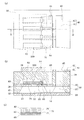
図1は、本発明の実施形態1に係る液体噴射ヘッドの概略を示す分解斜視図であり、図2は、図1の平面図(図2(a))及びA−A′断面図(図2(b))並びに圧電素子部の拡大図(図2(c))である。
Hereinafter, the present invention will be described in detail based on embodiments.
(Embodiment 1)
FIG. 1 is an exploded perspective view schematically showing a liquid jet head according to Embodiment 1 of the present invention, and FIG. 2 is a plan view of FIG. 2 (b)) and an enlarged view of the piezoelectric element portion (FIG. 2C).
図示するように、流路形成基板10は、本実施形態では面方位(110)のシリコン単結晶基板からなり、その一方面には二酸化シリコンからなる、厚さ0.5〜2μmの弾性膜50が形成されている。なお、この弾性膜50は、本実施形態では、シリコン単結晶基板である流路形成基板10を熱酸化することにより形成した酸化シリコンからなるアモルファス(非晶質)膜であり、流路形成基板10の表面状態をそのまま維持した平滑な表面状態を有している。また、この弾性膜50上には、酸化ジルコニウム(ZrO2)等の膜がさらに設けられていてもよい。
As shown in the drawing, the flow
この流路形成基板10には、シリコン単結晶基板をその一方面側から異方性エッチングすることにより、複数の隔壁11によって区画された圧力発生室12が幅方向に並設されている。また、その長手方向外側には、後述する保護基板30のリザーバ部32と連通される連通部13が形成されている。また、この連通部13は、各圧力発生室12の長手方向一端部でそれぞれインク供給路14を介して連通されている。なお、このインク供給路14の幅は、本実施形態では、圧力発生室12の幅よりも小さくなっており、連通部13から圧力発生室12に流入するインクの流路抵抗を一定に保持している。
In the flow
このような圧力発生室12等が形成される流路形成基板10の厚さは、圧力発生室12を配設する密度に合わせて最適な厚さを選択することが好ましい。例えば、1インチ当たり180個(180dpi)程度に圧力発生室12を配置する場合には、流路形成基板10の厚さは、180〜280μm程度、より望ましくは、220μm程度とするのが好適である。また、例えば、360dpi程度と比較的高密度に圧力発生室12を配置する場合には、流路形成基板10の厚さは、100μm以下とするのが好ましい。これは、隣接する圧力発生室12間の隔壁11の剛性を保ちつつ、配列密度を高くできるからである。
As the thickness of the flow
また、流路形成基板10の開口面側には、各圧力発生室12のインク供給路14とは反対側で連通するノズル開口21が穿設されたノズルプレート20が接着剤や熱溶着フィルム等を介して固着されている。
Further, a
一方、流路形成基板10の開口面とは反対側の弾性膜50の上には、厚さが例えば、約0.2μmの下電極膜60と、厚さが例えば、約1μmの圧電体層70と、厚さが例えば、約0.05μmの上電極膜80とからなる圧電素子300が形成されている。ここで、圧電素子300は、下電極膜60、圧電体層70、及び上電極膜80を含む部分をいう。一般的には、圧電素子300の何れか一方の電極を共通電極とし、他方の電極及び圧電体層70を圧力発生室12毎にパターニングして構成する。そして、ここではパターニングされた何れか一方の電極及び圧電体層70から構成され、両電極への電圧の印加により圧電歪みが生じる部分を圧電体能動部という。本実施形態では、下電極膜60は圧電素子300の共通電極とし、上電極膜80を圧電素子300の個別電極としているが、駆動回路や配線の都合でこれを逆にしても支障はない。何れの場合においても、圧力発生室毎に圧電体能動部が形成されていることになる。また、ここでは、圧電素子300と当該圧電素子300の駆動により変位が生じる振動板とを合わせてアクチュエータ装置と称する。
On the other hand, on the
なお、このような各圧電素子300の上電極膜80には、例えば、金(Au)等からなるリード電極85がそれぞれ接続されている。このリード電極85は、各圧電素子300の長手方向端部近傍から引き出され、インク供給路14に対応する領域の弾性膜50上にそれぞれ延設されて後述する駆動ICと接続されている。
Note that a
ここで、下電極膜60は、例えば、イリジウム(Ir)、白金(Pt)等の金属材料で形成されている。また、下電極膜60は、これらの金属材料からなる複数の層を積層したものであってもよい。なお、積層した場合には、後のプロセスにより、結果的に混合層となってもよい。下電極膜60の配向には特に制限はなく、例えば(111)配向でも、(100)配向でもよい。本実施形態では、白金(Pt)で(111)配向のものを下電極膜60とした。
Here, the
この下電極膜60上には、導電性の材料からなり面方位(100)のバッファ層65が0.5〜200nm程度の厚さで設けられている。バッファ層65上にエピタキシャル成長により形成される圧電体層70を面方位(100)とするためにバッファ層65は面方位(100)である必要があり、また、圧電素子300として機能するためにバッファ層65も導電性であることが必要である。なお、バッファ層65は、正方晶または立方晶であることが好ましい。
On the
また、バッファ層65は、後述する圧電体層本体75との格子定数、特にa軸の格子定数の差が8%以下であることが好ましい。このように格子定数の差が小さいと、圧電体層70を構成する組成傾斜層71及び圧電体層本体75を、バッファ層65上に良好にエピタキシャル成長させることができ、アクチュエータ装置としての変位が特に良好になる。
Further, the
バッファ層65の格子定数は、圧電体層本体75の格子定数よりも、大きくても小さくてもよい。圧電体層本体75をa軸の格子定数が4.03ÅのPZTとした場合、圧電体層本体75の格子定数(a軸)よりも大きな格子定数(a軸)を有するものとしては、MgO(a軸の格子定数は4.211Å。以下括弧内はa軸の格子定数を表す。)、TiO2(4.177Å)、NiO(4.177Å)、Cu2O(4.217Å)、NbO(4.211Å)等の金属酸化物、AlN(4.045Å)、TiN(4.242Å)、Ti2N(4.14Å)、TiAlN(4.112Å)、CrN(4.14Å)、CoN(4.28Å)等の金属窒化物、Al3Ni2(4.065Å)等の合金、MgNiO2(4.193Å)、CoNiO2(4.24Å)等の複合酸化物が挙げられる。しかしながら、後述するように製法上、バッファ層65の格子定数(a軸)は、圧電体層本体75の格子定数(a軸)よりも小さいことが好ましい。圧電体層本体75をa軸の格子定数が4.03ÅのPZTとした場合、4.03Åより小さい格子定数(a軸)を有するものとしては、WO3(3.714Å)等の金属酸化物、Al0.64Ti0.36(4.0296Å)、Al3Ti(3.972Å)、AlNi3(3.78Å)、CoTi(3.964Å)等の合金、CaTiO(3.895Å)、SrTiO(3.905Å)、Sr2TiO4(3.886Å)、SrCoO2.29(3.912Å)、ランタンニッケルオキサイド(LNO)(3.861Å)等の複合酸化物を挙げることができる。なお、本実施形態では、バッファ層65は、LNOであり、80nm程度の厚さとしている。
The lattice constant of the
圧電体層70は、チタン酸ジルコン酸鉛(PZT)からなる強誘電体薄膜であり、(100)面配向のバッファ層65上にエピタキシャル成長によって形成されている。そして、このように結晶がエピタキシャル成長した圧電体層70は、下地であるバッファ層65の拘束を受けて結晶化しているため、バッファ層65と同様に(100)面配向となっている。PZTからなる圧電体層70が面方位(100)であると、菱面体晶系であるとき、特に圧電特性を高めることができる。
The
この圧電体層70は、バッファ層65との境界部分に設けられ組成を厚さ方向に連続的に変化させた組成傾斜層71、及びこの組成傾斜層71上に積層された圧電体層本体75を有する。この組成傾斜層71は、例えば、10〜100nm程度の厚さを有し、圧電体層本体75は例えば、0.2〜5μm程度の厚さを有する。圧電体層本体75と同材料であるPZTからなる層が、バッファ層65と圧電体層本体75との間に存在しており、この層の組成を傾斜させることにより、バッファ層65と圧電体層70の格子定数を極めて近い値にできる。これにより、圧電体層70をエピタキシャル成長し易く、格子の不整合による応力がほとんど発生しない。なお、組成傾斜層71の存在によりバッファ層65と圧電体層70のa軸の格子定数を近い値にした場合は、b軸やc軸を調整した場合よりも、バッファ層と組成傾斜層、組成傾斜層と圧電体層本体の格子定数の不整合が小さくなるため、圧電体層をエピタキシャル成長し易く下地層との格子不整合による応力の発生が特に抑えられる。また、圧電体層本体75は実質的に組成傾斜していないことが好ましい。常に安定した圧電特性が得られるようにするためである。
The
ここで、組成傾斜とは、PZTを構成する元素の比率が、厚さ方向に連続的に変化していることをいい、例えば、Zr/Ti(モル比)が厚さ方向に徐々に減少している又は増大していることをいう。本実施形態の組成傾斜層71は、Zr/Ti(モル比)が厚さ方向に連続的に変化したものである。このようにZr/Ti(モル比)が変化すると、組成傾斜層71のa軸の格子定数は、厚さ方向に連続的に変化する。
Here, the composition gradient means that the ratio of elements constituting PZT changes continuously in the thickness direction. For example, Zr / Ti (molar ratio) gradually decreases in the thickness direction. It is said to be increasing or increasing. In the
本発明において、バッファ層65から厚さ方向に離れるにしたがって、組成傾斜層71の格子定数、特にa軸の格子定数は、バッファ層65の格子定数と圧電体層本体75の格子定数との間の値で、バッファ層65の格子定数に近い値から圧電体層本体75の格子定数に近い値へと連続的に変化する。すなわち、組成傾斜層71の格子定数は、バッファ層65側ではバッファ層65に近い値であり、厚さ方向にバッファ層65から離れるにしたがって徐々に小さくなる又は徐々に大きくなっていき、圧電体層本体75側では、圧電体層本体75の格子定数に近い値となる。
In the present invention, as the distance from the
具体的には、例えばバッファ層65の格子定数が圧電体層本体75の格子定数よりも大きい場合は、組成傾斜層71の格子定数は、バッファ層65に接する部分ではバッファ層65の格子定数に近い値であり、バッファ層65から厚さ方向に離れるにしたがって徐々に小さくなっていき、圧電体層本体75に接する部分では、圧電体層本体75の格子定数に近い値となる。一方、例えばバッファ層65の格子定数が圧電体層本体75の格子定数よりも小さい場合は、組成傾斜層71の格子定数は、バッファ層65に接する部分ではバッファ層65の格子定数に近い値であり、バッファ層65から厚さ方向に離れるにしたがって徐々に大きくなっていき、圧電体層本体75に接する部分では、圧電体層本体75の格子定数に近い値となる。
Specifically, for example, when the lattice constant of the
このように、バッファ層65の格子定数に近い値から圧電体層本体75の格子定数に近い値へと格子定数を一定方向に変化させた組成傾斜層71を間に有することで、バッファ層65上に圧電体層本体75を直接設けた場合よりも、格子定数の不整合が緩和されるため、応力の発生が抑えられる。また、組成傾斜層71の格子定数が連続的に変化するので、組成傾斜層71を形成する際にも応力の発生が抑制される。したがって圧電体層を構成するPZTの結晶系に歪みが生じないため、良好な変位を有するアクチュエータ装置となる。
As described above, the
特に、圧電体層本体75の格子定数(a軸)よりも格子定数(a軸)が小さいものをバッファ層65とし、Zr/Ti(モル比)をバッファ層65から厚さ方向に離れるにしたがって漸大させた組成傾斜層71とすることが好ましい。組成傾斜層71のZr/Ti(モル比)をバッファ層65から厚さ方向に離れるにしたがって漸大させることは簡便な方法で行えるので、容易に組成傾斜層71の格子定数(a軸)をバッファ層65から厚さ方向に離れるにしたがって漸大させることができるためである。詳述すると、後述する簡便な製造方法で製造すると、組成傾斜層71は、バッファ層65側ではZr/Tiが小さくバッファ層65から圧電体層本体75へと厚さ方向に離れるにしたがってZr/Tiが徐々に増大する。これは、組成傾斜層形成の初期にジルコニウムよりもチタンの酸化が進みジルコニアが微量でチタンの含有量が多いPZTがバッファ層65側に多く生成するためと推測される。このチタンの含有量が多いPZTのa軸の格子定数はチタン含有量のより少ないPZTよりも小さく、Zrが漸大するとa軸の格子定数は漸大するため、後述する簡便な製造方法で製造すると、組成傾斜層71のa軸の格子定数は、バッファ層65から圧電体層本体75へと厚さ方向に離れるにしたがって大きくなる。従って、製法上容易なので、圧電体層本体75の格子定数(a軸)よりも格子定数(a軸)が小さいものをバッファ層65とし、Zr/Ti(モル比)をバッファ層65から厚さ方向に離れるにしたがって漸大させた組成傾斜層71とすることが好ましい。
In particular, the
圧電体層本体75は特に限定されないが、a軸の格子定数が4.03Å前後のチタン酸ジルコン酸鉛(Pb1.14〜1.25(Zr0.50〜0.55Ti0.50〜0.45)O3)であることが好ましい。本実施形態では圧電体層本体75としてPb1.18(Zr0.516Ti0.484)O3を用い、また、バッファ層65としてa軸の格子定数が3.861Åで、圧電体層本体75との格子定数(a軸)の差が4.19%であるLNOを用いて、厚さ10nmの組成傾斜層71と厚さ1μmの圧電体層本体75からなる圧電体層70を設けている。この、組成傾斜層71は、バッファ層65から厚さ方向に離れるにしたがって、Zr/Ti(モル比)が実質的に0から1へと徐々に変化するようにし、組成傾斜層71の格子定数(a軸)を徐々に圧電体層本体75の4.03Åに近づくように形成した。このような組成傾斜層71を間に設けることにより、下地(バッファ層65)と圧電体層70の格子不整合が緩和されるので、当該下地上に設けた圧電体層70に発生する応力が低減され、結晶系に歪みのない圧電体層70となる。
The
このような圧電素子300が設けられた側の流路形成基板10上には、圧電素子300の運動を阻害しない程度の空間を確保する圧電素子保持部31を有する保護基板30が接合され、圧電素子300はこの圧電素子保持部31内に形成されている。なおこの圧電素子保持部31は、空間が密封されていてもよいし、密封されていなくてもよい。また、保護基板30には、各圧力発生室12に共通するリザーバ90の少なくとも一部を構成するリザーバ部32が設けられ、このリザーバ部32は、上述のように流路形成基板10の連通部13と連通されてリザーバ90を構成している。
A
さらに、保護基板30の圧電素子保持部31とリザーバ部32との間には、この保護基板30を厚さ方向に貫通する接続孔33が設けられている。また、保護基板30の圧電素子保持部31側とは反対側の表面には、各圧電素子300を駆動するための駆動IC34が実装されている。そして、各圧電素子300から引き出されたリード電極85は、接続孔33まで延設されており、図示しないが、例えば、ワイヤボンディング等からなる接続配線を介して駆動IC34と接続されている。
Further, a
保護基板30上には、封止膜41及び固定板42とからなるコンプライアンス基板40が接合されている。ここで、封止膜41は、剛性が低く可撓性を有する材料(例えば、厚さが6μmのポリフェニレンサルファイド(PPS)フィルム)からなる。また、固定板42は、金属等の硬質の材料(例えば、厚さが30μmのステンレス鋼(SUS)等)で形成される。この固定板42のリザーバ90に対向する領域には、厚さ方向に完全に除去された開口部43が形成され、リザーバ90の一方面は可撓性を有する封止膜41のみで封止されている。
On the
なお、このような液体噴射ヘッドは、図示しない外部液体供給手段から液体を取り込み、リザーバ90からノズル開口21に至るまで内部を液体で満たした後、図示しない駆動回路からの記録信号に従い、圧力発生室12に対応するそれぞれの下電極膜60と上電極膜80との間に電圧を印加し、弾性膜50、下電極膜60及び圧電体層70をたわみ変形させることにより、各圧力発生室12内の圧力が高まりノズル開口21から液滴が吐出する。
Such a liquid ejecting head takes in liquid from an external liquid supply means (not shown), fills the interior from the
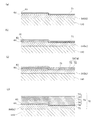
ここで、このようなインクジェット式記録ヘッドの製造方法について、図3〜図7を参照して説明する。なお、図3〜図7は、圧力発生室12の長手方向の断面図である。まず、図3(a)に示すように、シリコンウェハである流路形成基板用ウェハ110を約1100℃の拡散炉で熱酸化し、その表面に弾性膜50を構成する二酸化シリコン膜51を形成する。なお、上述したように、この二酸化シリコン膜51は、アモルファス膜である。また、本実施形態では、流路形成基板用ウェハ110として、膜厚が約625μmと比較的厚く剛性の高いシリコンウェハを用いている。
Here, a method of manufacturing such an ink jet recording head will be described with reference to FIGS. 3 to 7 are cross-sectional views of the
次に、図3(b)に示すように、弾性膜50上に下電極膜60を形成する。例えば、本実施形態では、流路形成基板用ウェハ110の全面に、スパッタリング法によって白金(Pt)からなる金属層61を形成し、その後、この金属層61を所定形状にパターニングすることによって下電極膜60を形成した。このように形成された下電極膜60は、面方位(111)となる。
Next, as shown in FIG. 3B, the
その後、図3(c)に示すように、この下電極膜60上に、導電性材料からなる面方位(100)のバッファ層65を形成する。本実施形態では、スパッタリング法によりLNO(100)のバッファ層65を形成している。なお、このバッファ層65の厚さは特に限定されないが、例えば、0.5nm〜200nm程度の厚さであることが好ましく、本実施形態では、80nm程度としている。
Thereafter, as shown in FIG. 3C, a
次いで、図4に示すように、このバッファ層65上に、チタン酸ジルコン酸鉛(PZT)からなる圧電体層70を形成する。本実施形態では、Pb、Zr及びTiをそれぞれ含む金属有機物を触媒に溶解・分散したいわゆるゾルを塗布乾燥してゲル化し、さらに高温で焼成することでPZTからなる圧電体層70を得る、いわゆるゾル−ゲル法を用いて圧電体層70を形成した。なお、圧電体層70はエピタキシャル成長により製造されていればゾル−ゲル法に限定されず、例えば、スパッタリング法、MOCVD法(有機金属気相成長法)やMOD(Metal-Organic Decomposition)法等であってもよい。
Next, as shown in FIG. 4, a
具体的には、バッファ層65上に、まず組成傾斜層71を形成する(図4(a))。組成傾斜層71の形成手順としては、まず、バッファ層65上にPZTを構成する金属を含む膜(PZT前駆体膜)を成膜する。すなわち、バッファ層65上に、Pb、Zr及びTiをそれぞれ含む金属有機物を含むゾル(溶液)を塗布する(塗布工程)。次いで、PZT前駆体膜を、例えば、140℃〜170℃で、5〜50分間程度加熱させてゾルの溶媒を蒸発させることで、PZT前駆体膜を乾燥させる(乾燥工程)。本実施形態では、140℃で5分間加熱した。
Specifically, the
その後、このPZT前駆体膜を180〜350℃、好ましくは200〜240℃、さらに好ましくは220℃に加熱して、その温度で一定時間、例えば5〜60分間加熱する(組成傾斜工程)。400℃より高温に昇温する前に180〜350℃で一定時間保持することにより、後述する脱脂工程及び焼成工程後の組成傾斜層71は、バッファ層65側から圧電体層本体75側にいくにしたがって、Zr/Ti(モル比)が徐々に増大する。180〜350℃で一定時間加熱することにより、ジルコニウムよりもチタンの酸化が進みジルコニアが微量でチタンの含有量が多いPZTがバッファ層65側に多く生成するため、バッファ層65側がTiリッチな組成傾斜層71が製造されるものと推測される。なお、本実施形態では、220℃で20分間加熱した。
Thereafter, the PZT precursor film is heated to 180 to 350 ° C., preferably 200 to 240 ° C., more preferably 220 ° C., and heated at that temperature for a certain time, for example, 5 to 60 minutes (composition gradient step). By keeping the temperature at 180 to 350 ° C. for a certain period of time before raising the temperature from 400 ° C. to higher than 400 ° C., the
このように、PZT前駆体膜を焼成工程前に180〜350℃で一定時間保持させることにより、Zr/Ti組成を傾斜させた組成傾斜層71を得ることができる。なお、この組成傾斜工程でゾルの溶媒の除去が併せて行えるのであれば、上述の乾燥工程は省略してもよい。
In this way, by maintaining the PZT precursor film at 180 to 350 ° C. for a predetermined time before the firing step, it is possible to obtain the
次いで、一定の温度で一定時間、例えば、350〜450℃で15〜30分程度PZT前駆体膜を脱脂する(脱脂工程)。なお、ここで言う脱脂とは、ゾル膜の有機成分を、例えば、NO2、CO2、H2O等として離脱させることである。本実施形態では、400℃で10分間加熱した。ただし、上記組成傾斜工程で脱脂が併せて行えるのであれば、この脱脂工程は省略してもよい。 Next, the PZT precursor film is degreased at a certain temperature for a certain time, for example, at 350 to 450 ° C. for about 15 to 30 minutes (degreasing step). Here, degreasing refers, the organic components of the sol film, for example, is to be detached as NO 2, CO 2, H 2 O or the like. In this embodiment, heating was performed at 400 ° C. for 10 minutes. However, this degreasing step may be omitted if degreasing can be performed in the composition gradient step.
その後、このPZT前駆体膜を、例えば680〜900℃で5〜30分程度加熱処理することによって、結晶化させて組成傾斜層71を形成する(焼成工程)。本実施形態では、680℃で5分間加熱した。このように形成した組成傾斜層71は(100)面配向のバッファ層65上にエピタキシャル成長しており、結晶は(100)面に優先配向する。なお、優先配向とは、結晶の配向方向が無秩序ではなく、特定の結晶面がほぼ一定の方向に向いている状態をいう。
Thereafter, the PZT precursor film is crystallized by, for example, heat treatment at 680 to 900 ° C. for about 5 to 30 minutes to form the composition gradient layer 71 (firing step). In this embodiment, heating was performed at 680 ° C. for 5 minutes. The
ここで、乾燥工程、組成傾斜工程、脱脂工程及び焼成工程で用いる加熱装置としては、例えば、ホットプレートや赤外線ランプの照射により加熱するRTA(Rapid Thermal Annealing)装置などが挙げられる。 Here, examples of the heating device used in the drying step, the composition gradient step, the degreasing step, and the firing step include an RTA (Rapid Thermal Annealing) device that heats by irradiation with a hot plate or an infrared lamp.
次に、組成傾斜層71上にPZTからなる圧電体層本体75を形成する。本実施形態では、ゾル−ゲル法を用いて圧電体層本体75を形成している。圧電体層本体75は、塗布工程、脱脂工程及び焼成工程を順に行うことにより製造することができ、各工程の製造条件は、上記組成傾斜層71の製造における各工程と同様の条件とすることができる。すなわち、上記組成傾斜層71の製造方法において、組成傾斜工程を行わないことで、製造することができる。なお、圧電体層本体75は実質的に組成傾斜していないことが好ましい。常に安定した圧電特性が得られるようにするためである。実質的に組成傾斜していない圧電体層本体75の具体的な形成方法を、以下に例示する。
Next, a
まず、図4(b)に示すように、組成傾斜層71上に、Pb、Zr及びTiをそれぞれ含む金属有機物を含むゾル(溶液)を塗布しPZT前駆体膜72を形成する(塗布工程)。次いで、PZT前駆体膜72を、室温からゾルの主溶媒である溶剤の沸点よりも低い温度に加熱して一定時間乾燥させ、ゾルの溶媒を蒸発させることでPZT前駆体膜72を乾燥させる(第1の乾燥工程)。
First, as shown in FIG. 4B, a sol (solution) containing a metal organic material containing Pb, Zr and Ti is applied on the
ここで、ゾルの主溶媒は、特に限定されないが、例えば、エタノール系の溶剤を用いることが好ましく、本実施形態では、沸点が176℃である2−n−ブトキシエタノールを用いている。このため、本実施形態では、第1の乾燥工程において、塗布したゾルを溶剤の沸点である176℃以下、例えば、約140℃程度に加熱して3分間程度保持することで、PZT前駆体膜72を乾燥させている。
Here, the main solvent of the sol is not particularly limited, but for example, an ethanol-based solvent is preferably used, and in this embodiment, 2-n-butoxyethanol having a boiling point of 176 ° C. is used. For this reason, in the present embodiment, in the first drying step, the applied sol is heated to a boiling point of the solvent of 176 ° C. or lower, for example, about 140 ° C. and held for about 3 minutes, whereby the
次いで、PZT前駆体膜72を再び加熱することにより、例えば、本実施形態では、第1の乾燥工程よりも高い温度まで上昇させて一定時間保持し、ゾルの主溶媒をさらに蒸発させてPZT前駆体膜72を乾燥させる(第2の乾燥工程)。第2の乾燥工程における到達温度は、140℃〜170℃に設定されている。乾燥時間は、5〜50分間程度であることが好ましい。
Next, by heating the
このような乾燥工程で用いる加熱装置としては、例えば、クリーンオーブン(拡散炉)、あるいはベーク装置等が挙げられるが、特に、ベーク装置を用いることが好ましい。クリーンオーブンでは、熱風を当てることによって温度を制御しているため、流路形成基板用ウェハの面内方向で、PZT前駆体膜の特性がばらつきやすいからである。 Examples of the heating device used in such a drying step include a clean oven (diffusion furnace), a baking device, and the like. In particular, it is preferable to use a baking device. This is because in a clean oven, the temperature is controlled by applying hot air, so that the characteristics of the PZT precursor film are likely to vary in the in-plane direction of the flow path forming substrate wafer.
このような第1及び第2の乾燥工程によってPZT前駆体膜72を乾燥後、上記組成傾斜層71の形成の際に記載した組成傾斜工程を経ずに、さらに大気雰囲気下において一定の温度で一定時間、PZT前駆体膜72を脱脂する(脱脂工程)。
After the
脱脂工程における加熱方法は、特に限定されないが、本実施形態では、ホットプレート上に流路形成基板用ウェハを載置して、PZT前駆体膜72を所定の温度まで上昇させている。昇温レートを低下させる際には、流路形成基板用ウェハ110よりも外径が若干大きい所定厚さのアルミ板である治具を介してウェハを加熱することとしている。脱脂工程での脱脂温度は、350℃〜450℃の範囲の温度に設定されている。
The heating method in the degreasing step is not particularly limited, but in this embodiment, the flow path forming substrate wafer is placed on the hot plate, and the
また、圧電体層70の結晶性を向上させるためには、脱脂工程における昇温レートが重要である。具体的には、脱脂工程における昇温レートは15[℃/sec]以上にされている。なお、ここで言う「昇温レート」とは、加熱開始時の温度(室温)と到達温度との温度差の20%上昇した温度から、温度差の80%の温度に達するまでの温度の時間変化率と規定する。例えば、室温25℃から100℃まで50秒で昇温させた場合の昇温レートは、(100−25)×(0.8−0.2)/50=0.9[℃/sec]となる。
Further, in order to improve the crystallinity of the
そして、このような塗布工程・第1の乾燥工程・第2の乾燥工程・脱脂工程を所定回数、例えば、本実施形態では、2回繰り返すことで、図4(c)に示すように、所定厚のPZT前駆体膜73を形成する。なお、本実施形態では、塗布工程・第1の乾燥・第2の乾燥・脱脂工程を2回繰り返すことで所定厚のPZT前駆体膜73を形成したが、勿論、繰り返し回数は2回に限らず、1回のみでもよいし、3回以上でもよい。
Then, by repeating the coating process, the first drying process, the second drying process, and the degreasing process a predetermined number of times, for example, twice in this embodiment, as shown in FIG. A thick
その後、このPZT前駆体膜73を加熱処理することによって結晶化させ、圧電体膜74を形成する(焼成工程)。本実施形態では、例えば、680℃以上で5〜30分間加熱を行ってPZT前駆体膜73を焼成して圧電体膜74を形成した。加熱装置としては、RTA(Rapid Thermal Annealing)装置が使用され、焼成工程の昇温レートは100[℃/sec]〜150[℃/sec]に設定され、急速加熱されるようになっている。
Thereafter, the
そして、上述した塗布工程・第1及び第2の乾燥工程・脱脂工程・焼成工程を、複数回繰り返すことで、図4(d)に示すように、複数層、本実施形態では、5層の圧電体膜74からなる所定厚さの圧電体層本体75を形成する。例えば、ゾルの塗布1回あたりの膜厚が0.1μm程度の場合には、圧電体層本体75全体の膜厚は約1μmとなる。このようにして得られた圧電体層本体75は、組成が実質的に傾斜していない。この圧電体層本体75と組成傾斜層71とで、圧電体層70となる。
And by repeating the application | coating process, 1st and 2nd drying process, degreasing process, and baking process mentioned above several times, as shown in FIG.4 (d), as shown in FIG.4 (d), in this embodiment, 5 layers. A piezoelectric layer
以上述べたように、非常に簡単な方法で、Zr/Tiを漸大させた組成傾斜層71をバッファ層65との境界部分に有する圧電体層70を得ることができる。このような組成傾斜層71は格子定数(a軸)がバッファ層65から圧電体層本体75に向けて漸大しており、この組成傾斜層71がバッファ層65と圧電体層本体75との間に挟まれているため、圧電体層70とバッファ層65との格子定数の不整合が緩和される。したがって、バッファ層65上に圧電体層70をエピタキシャル成長により設ける際に発生する応力が抑制されるため、結晶歪のない圧電体層70を得ることができる。よって、本発明の製造方法によれば、圧電特性が大幅に向上したアクチュエータ装置となる。なお、バッファ層65を圧電体層本体75よりも大きい格子定数を有するものとした場合、組成傾斜層71の格子定数がバッファ層65から離れるにしたがって漸小する、すなわち、Zr/Tiが漸小するように組成傾斜層71を製造するには、例えば、触媒等を添加して、チタンよりもジルコニウムの酸化を促進させることにより、ジルコニウムの含有量が多いPZTをバッファ層65側に多く生成させる等の方法で行えばよい。
As described above, the
このように圧電体層70を形成した後は(図5(a))、図5(b)に示すように、例えば、イリジウムからなる上電極膜80を流路形成基板用ウェハ110の全面に形成する。次いで、図5(c)に示すように、バッファ層65、圧電体層70及び上電極膜80を各圧力発生室に対向する領域にパターニングして圧電素子300を形成する。次いで、図6(a)に示すように、流路形成基板用ウェハ110の全面に亘って、例えば、金(Au)等からなる金属層86を形成し、その後、この金属層86を圧電素子300毎にパターニングすることによりリード電極85を形成する。
After the
次に、図6(b)に示すように、流路形成基板用ウェハ110の圧電素子300側に、例えば、厚さが400nm程度のシリコンウェハからなり複数の保護基板30となる保護基板用ウェハ130を接合する。次いで、図6(c)に示すように、流路形成基板用ウェハ110をある程度の厚さとなるまで研磨した後、さらにフッ硝酸によってウェットエッチングすることにより流路形成基板用ウェハ110を所定の厚みにする。次いで、図7(a)に示すように、流路形成基板用ウェハ110上に、例えば、窒化シリコン(SiN)からなるマスク膜52を新たに形成し、所定形状にパターニングする。そして、このマスク膜52を介して流路形成基板用ウェハ110を異方性エッチングすることにより、図7(b)に示すように、流路形成基板用ウェハ110に圧力発生室12、連通部13及びインク供給路14等を形成する。
Next, as shown in FIG. 6B, the protective substrate wafer is formed of, for example, a silicon wafer having a thickness of about 400 nm on the side of the
なお、その後は、流路形成基板用ウェハ110及び保護基板用ウェハ130の外周縁部の不要部分を、例えば、ダイシング等により切断することによって除去する。そして、流路形成基板用ウェハ110の保護基板用ウェハ130とは反対側の面にノズル開口21が穿設されたノズルプレート20を接合すると共に、保護基板用ウェハ130にコンプライアンス基板40を接合し、流路形成基板用ウェハ110等を図1に示すような一つのチップサイズの流路形成基板10等に分割することによってインクジェット式記録ヘッドとする。
After that, unnecessary portions of the outer peripheral edge portions of the flow path forming
(他の実施形態)
以上、本発明の実施形態を説明したが、本発明の構成は上述したものに限定されるものではない。また、このような本発明の液体噴射ヘッドは、液体カートリッジ等と連通する液体流路を具備する噴射ヘッドユニットの一部を構成して、液体噴射装置に搭載される。図8は、その液体噴射装置の一例を示す概略図である。
(Other embodiments)
As mentioned above, although embodiment of this invention was described, the structure of this invention is not limited to what was mentioned above. In addition, such a liquid jet head according to the present invention constitutes a part of a jet head unit including a liquid flow path communicating with a liquid cartridge or the like, and is mounted on the liquid jet apparatus. FIG. 8 is a schematic diagram illustrating an example of the liquid ejecting apparatus.
図8に示すように、液体噴射ヘッドを有する噴射ヘッドユニット1A及び1Bは、液体供給手段を構成するカートリッジ2A及び2Bが着脱可能に設けられ、この噴射ヘッドユニット1A及び1Bを搭載したキャリッジ3は、装置本体4に取り付けられたキャリッジ軸5に軸方向移動自在に設けられている。この噴射ヘッドユニット1A及び1Bは、液体として、例えば、それぞれブラックインク組成物及びカラーインク組成物を吐出するものとしている。
As shown in FIG. 8, in the
そして、駆動モータ6の駆動力が図示しない複数の歯車およびタイミングベルト7を介してキャリッジ3に伝達されることで、噴射ヘッドユニット1A及び1Bを搭載したキャリッジ3はキャリッジ軸5に沿って移動される。一方、装置本体4にはキャリッジ軸5に沿ってプラテン8が設けられており、図示しない給紙ローラなどにより給紙された紙等の記録媒体である記録シートSがプラテン8上に搬送されるようになっている。
Then, the driving force of the driving
また、本発明の基本的構成は上述したものに限定されるものではない。本発明は、広く液体噴射ヘッドの全般を対象としたものであり、例えば、プリンタ等の画像記録装置に用いられるインクジェット式記録ヘッド等の各種の記録ヘッド、液晶ディスプレー等のカラーフィルタの製造に用いられる色材噴射ヘッド、有機ELディスプレー、FED(面発光ディスプレー)等の電極形成に用いられる電極材料噴射ヘッド、バイオchip製造に用いられる生体有機物噴射ヘッド等にも適用することができる。勿論、このような液体噴射ヘッドを搭載した液体噴射装置も特に限定されるものではない。さらに、本発明は、液体噴射ヘッドに利用されるアクチュエータ装置に限定されず、他のあらゆる装置に搭載されるアクチュエータ装置にも適用できる。例えば、アクチュエータ装置は、上述したヘッドの他に、センサー等にも適用することができる。 The basic configuration of the present invention is not limited to the above-described one. The present invention covers a wide range of liquid ejecting heads, and is used for manufacturing various recording heads such as ink jet recording heads used in image recording apparatuses such as printers and color filters such as liquid crystal displays. The present invention can also be applied to a color material ejecting head, an organic EL display, an electrode material ejecting head used for forming an electrode such as an FED (surface emitting display), a bioorganic matter ejecting head used for biochip production, and the like. Needless to say, a liquid ejecting apparatus including such a liquid ejecting head is not particularly limited. Furthermore, the present invention is not limited to an actuator device used for a liquid ejecting head, and can also be applied to an actuator device mounted on any other device. For example, the actuator device can be applied to a sensor or the like in addition to the head described above.
10 流路形成基板、11 隔壁、12 圧力発生室、13 連通部、14 インク供給路、20 ノズルプレート、21 ノズル開口、30 保護基板、31 圧電素子保持部、32 リザーバ部、40 コンプライアンス基板、50 弾性膜、60 下電極膜、65 バッファ層、70 圧電体層、71 組成傾斜層、74 圧電体膜、75 圧電体層本体、80 上電極膜、90 リザーバ
DESCRIPTION OF
Claims (6)
前記バッファ層上にエピタキシャル成長によりPb、Zr、Tiを含むペロブスカイト構造を有する金属酸化物からなる圧電体層を形成する工程と、
前記圧電体層上に上電極を形成する工程とを備え、
前記圧電体層を形成する工程で、前記バッファ層上に形成したPb、Zr、Tiを含む前駆体膜を400℃以上に昇温する前に180〜350℃で一定時間保持した後、焼成することにより組成を厚さ方向に連続的に変化させた組成傾斜層を形成し、この組成傾斜層上にPb、Zr、Tiを含むペロブスカイト構造を有する金属酸化物からなる圧電体層本体を積層し前記組成傾斜層と前記圧電体層本体とで前記圧電体層とすることを特徴とする圧電素子の製造方法。 Forming a surface orientation (100) buffer layer made of a conductive material on the lower electrode;
Forming a piezoelectric layer made of a metal oxide having a perovskite structure containing Pb, Zr, Ti by epitaxial growth on the buffer layer;
Forming an upper electrode on the piezoelectric layer,
In the step of forming the piezoelectric layer, the precursor film containing Pb, Zr, and Ti formed on the buffer layer is held at 180 to 350 ° C. for a predetermined time before being heated to 400 ° C. or higher, and then fired. Thus, a composition gradient layer whose composition is continuously changed in the thickness direction is formed, and a piezoelectric layer body made of a metal oxide having a perovskite structure containing Pb, Zr, Ti is laminated on the composition gradient layer. A method for manufacturing a piezoelectric element , wherein the composition gradient layer and the piezoelectric layer main body constitute the piezoelectric layer.
Priority Applications (1)
| Application Number | Priority Date | Filing Date | Title |
|---|---|---|---|
| JP2005227677A JP5007780B2 (en) | 2005-08-05 | 2005-08-05 | Piezoelectric element manufacturing method, liquid ejecting head manufacturing method, and liquid ejecting apparatus manufacturing method |
Applications Claiming Priority (1)
| Application Number | Priority Date | Filing Date | Title |
|---|---|---|---|
| JP2005227677A JP5007780B2 (en) | 2005-08-05 | 2005-08-05 | Piezoelectric element manufacturing method, liquid ejecting head manufacturing method, and liquid ejecting apparatus manufacturing method |
Publications (3)
| Publication Number | Publication Date |
|---|---|
| JP2007042983A JP2007042983A (en) | 2007-02-15 |
| JP2007042983A5 JP2007042983A5 (en) | 2008-09-18 |
| JP5007780B2 true JP5007780B2 (en) | 2012-08-22 |
Family
ID=37800666
Family Applications (1)
| Application Number | Title | Priority Date | Filing Date |
|---|---|---|---|
| JP2005227677A Active JP5007780B2 (en) | 2005-08-05 | 2005-08-05 | Piezoelectric element manufacturing method, liquid ejecting head manufacturing method, and liquid ejecting apparatus manufacturing method |
Country Status (1)
| Country | Link |
|---|---|
| JP (1) | JP5007780B2 (en) |
Families Citing this family (5)
| Publication number | Priority date | Publication date | Assignee | Title |
|---|---|---|---|---|
| JP5056139B2 (en) * | 2007-04-20 | 2012-10-24 | 日立電線株式会社 | Piezoelectric thin film element |
| JP5754198B2 (en) * | 2011-03-24 | 2015-07-29 | セイコーエプソン株式会社 | Liquid ejecting head, liquid ejecting apparatus, and piezoelectric actuator |
| WO2014024695A1 (en) * | 2012-08-08 | 2014-02-13 | コニカミノルタ株式会社 | Piezoelectric element, piezoelectric device, ink-jet head, and ink-jet printer |
| JP6596634B2 (en) | 2014-10-23 | 2019-10-30 | アドバンストマテリアルテクノロジーズ株式会社 | Ferroelectric ceramics, electronic parts, and manufacturing method of ferroelectric ceramics |
| CN109829203B (en) * | 2019-01-07 | 2020-11-24 | 重庆大学 | Production method of fabric base material in building space membrane structure |
Family Cites Families (4)
| Publication number | Priority date | Publication date | Assignee | Title |
|---|---|---|---|---|
| JP3482883B2 (en) * | 1998-08-24 | 2004-01-06 | 株式会社村田製作所 | Ferroelectric thin film element and method of manufacturing the same |
| JP2004066600A (en) * | 2002-08-05 | 2004-03-04 | Seiko Epson Corp | Liquid ejection head and liquid ejector |
| JP4521751B2 (en) * | 2003-03-26 | 2010-08-11 | 国立大学法人東京工業大学 | Lead zirconate titanate-based film, dielectric element, and method for manufacturing dielectric film |
| JP2004296919A (en) * | 2003-03-27 | 2004-10-21 | Seiko Epson Corp | Process for fabricating capacitor, memory, and electronic apparatus |
-
2005
- 2005-08-05 JP JP2005227677A patent/JP5007780B2/en active Active
Also Published As
| Publication number | Publication date |
|---|---|
| JP2007042983A (en) | 2007-02-15 |
Similar Documents
| Publication | Publication Date | Title |
|---|---|---|
| JP4984018B2 (en) | Piezoelectric element, liquid ejecting head, and liquid ejecting apparatus | |
| JP4333686B2 (en) | Actuator device, liquid jet head, and liquid jet device | |
| JP5251031B2 (en) | Piezoelectric element, liquid ejecting head, liquid ejecting apparatus, sensor | |
| JP5158299B2 (en) | Piezoelectric element, actuator device, liquid ejecting head, liquid ejecting apparatus, and method of manufacturing piezoelectric element | |
| JP5007780B2 (en) | Piezoelectric element manufacturing method, liquid ejecting head manufacturing method, and liquid ejecting apparatus manufacturing method | |
| JP5737540B2 (en) | Piezoelectric element, liquid ejecting head, sensor and motor | |
| JP5741799B2 (en) | Liquid ejecting head, liquid ejecting apparatus, and piezoelectric element | |
| JP5578311B2 (en) | Liquid ejecting head, liquid ejecting apparatus, and method of manufacturing liquid ejecting head | |
| JP2010241021A (en) | Liquid-ejecting head, liquid-ejecting apparatus, and actuator | |
| JP5858209B2 (en) | Method for manufacturing piezoelectric element and method for manufacturing liquid jet head | |
| JP5152461B2 (en) | Piezoelectric element, manufacturing method thereof, liquid jet head, and liquid jet apparatus | |
| JP2006286911A (en) | Piezoelectric element, liquid injection head, and liquid injection apparatus using the same | |
| JP2011181556A (en) | Method for manufacturing actuator | |
| JP2006261412A (en) | Piezoelectric element, manufacturing method thereof, liquid jetting head using same piezoelectric element, and liquid jetting apparatus | |
| JP5104609B2 (en) | Liquid ejecting head, liquid ejecting apparatus, and piezoelectric element | |
| JP5304976B2 (en) | Method for manufacturing laminated film, method for manufacturing actuator device, method for manufacturing liquid jet head, and actuator device | |
| JP2011238710A (en) | Manufacturing method of liquid injection head and liquid injection device using the same, and manufacturing method of piezo-electric element | |
| JP2007042949A (en) | Method of manufacturing piezoelectric element and piezoelectric element as well as liquid injection head and liquid injection device | |
| JP5716939B2 (en) | Liquid ejecting head, liquid ejecting apparatus, and actuator device | |
| JP2009076819A (en) | Actuator device, liquid jetting head and liquid jetting device | |
| JP6083190B2 (en) | Liquid ejecting head, liquid ejecting apparatus, and actuator device | |
| US8529024B2 (en) | Piezoelectric element, liquid ejecting head, and liquid ejecting apparatus | |
| JP5670017B2 (en) | Liquid ejecting head, liquid ejecting apparatus, and actuator device | |
| JP5679636B2 (en) | Liquid ejecting head and actuator device | |
| JP2006216685A (en) | Single crystal ferroelectric thin film, liquid injection head using the same and liquid fuel injection device |
Legal Events
| Date | Code | Title | Description |
|---|---|---|---|
| A521 | Request for written amendment filed |
Free format text: JAPANESE INTERMEDIATE CODE: A523 Effective date: 20080804 |
|
| A621 | Written request for application examination |
Free format text: JAPANESE INTERMEDIATE CODE: A621 Effective date: 20080804 |
|
| A977 | Report on retrieval |
Free format text: JAPANESE INTERMEDIATE CODE: A971007 Effective date: 20120105 |
|
| A131 | Notification of reasons for refusal |
Free format text: JAPANESE INTERMEDIATE CODE: A131 Effective date: 20120201 |
|
| A521 | Request for written amendment filed |
Free format text: JAPANESE INTERMEDIATE CODE: A523 Effective date: 20120402 |
|
| TRDD | Decision of grant or rejection written | ||
| A01 | Written decision to grant a patent or to grant a registration (utility model) |
Free format text: JAPANESE INTERMEDIATE CODE: A01 Effective date: 20120502 |
|
| A01 | Written decision to grant a patent or to grant a registration (utility model) |
Free format text: JAPANESE INTERMEDIATE CODE: A01 |
|
| A61 | First payment of annual fees (during grant procedure) |
Free format text: JAPANESE INTERMEDIATE CODE: A61 Effective date: 20120515 |
|
| R150 | Certificate of patent or registration of utility model |
Free format text: JAPANESE INTERMEDIATE CODE: R150 Ref document number: 5007780 Country of ref document: JP Free format text: JAPANESE INTERMEDIATE CODE: R150 |
|
| FPAY | Renewal fee payment (event date is renewal date of database) |
Free format text: PAYMENT UNTIL: 20150608 Year of fee payment: 3 |
|
| S531 | Written request for registration of change of domicile |
Free format text: JAPANESE INTERMEDIATE CODE: R313531 |
|
| R350 | Written notification of registration of transfer |
Free format text: JAPANESE INTERMEDIATE CODE: R350 |