JP4989552B2 - Electronic components - Google Patents
Electronic components Download PDFInfo
- Publication number
- JP4989552B2 JP4989552B2 JP2008122368A JP2008122368A JP4989552B2 JP 4989552 B2 JP4989552 B2 JP 4989552B2 JP 2008122368 A JP2008122368 A JP 2008122368A JP 2008122368 A JP2008122368 A JP 2008122368A JP 4989552 B2 JP4989552 B2 JP 4989552B2
- Authority
- JP
- Japan
- Prior art keywords
- electronic component
- recess
- stress
- heat
- insulating member
- Prior art date
- Legal status (The legal status is an assumption and is not a legal conclusion. Google has not performed a legal analysis and makes no representation as to the accuracy of the status listed.)
- Expired - Fee Related
Links
Images


Classifications
-
- H—ELECTRICITY
- H10—SEMICONDUCTOR DEVICES; ELECTRIC SOLID-STATE DEVICES NOT OTHERWISE PROVIDED FOR
- H10W—GENERIC PACKAGES, INTERCONNECTIONS, CONNECTORS OR OTHER CONSTRUCTIONAL DETAILS OF DEVICES COVERED BY CLASS H10
- H10W40/00—Arrangements for thermal protection or thermal control
- H10W40/20—Arrangements for cooling
- H10W40/22—Arrangements for cooling characterised by their shape, e.g. having conical or cylindrical projections
-
- H—ELECTRICITY
- H05—ELECTRIC TECHNIQUES NOT OTHERWISE PROVIDED FOR
- H05K—PRINTED CIRCUITS; CASINGS OR CONSTRUCTIONAL DETAILS OF ELECTRIC APPARATUS; MANUFACTURE OF ASSEMBLAGES OF ELECTRICAL COMPONENTS
- H05K3/00—Apparatus or processes for manufacturing printed circuits
- H05K3/0058—Laminating printed circuit boards onto other substrates, e.g. metallic substrates
- H05K3/0061—Laminating printed circuit boards onto other substrates, e.g. metallic substrates onto a metallic substrate, e.g. a heat sink
-
- H—ELECTRICITY
- H05—ELECTRIC TECHNIQUES NOT OTHERWISE PROVIDED FOR
- H05K—PRINTED CIRCUITS; CASINGS OR CONSTRUCTIONAL DETAILS OF ELECTRIC APPARATUS; MANUFACTURE OF ASSEMBLAGES OF ELECTRICAL COMPONENTS
- H05K1/00—Printed circuits
- H05K1/02—Details
- H05K1/03—Use of materials for the substrate
- H05K1/0306—Inorganic insulating substrates, e.g. ceramic, glass
-
- H—ELECTRICITY
- H05—ELECTRIC TECHNIQUES NOT OTHERWISE PROVIDED FOR
- H05K—PRINTED CIRCUITS; CASINGS OR CONSTRUCTIONAL DETAILS OF ELECTRIC APPARATUS; MANUFACTURE OF ASSEMBLAGES OF ELECTRICAL COMPONENTS
- H05K2201/00—Indexing scheme relating to printed circuits covered by H05K1/00
- H05K2201/09—Shape and layout
- H05K2201/09009—Substrate related
- H05K2201/09054—Raised area or protrusion of metal substrate
-
- H—ELECTRICITY
- H05—ELECTRIC TECHNIQUES NOT OTHERWISE PROVIDED FOR
- H05K—PRINTED CIRCUITS; CASINGS OR CONSTRUCTIONAL DETAILS OF ELECTRIC APPARATUS; MANUFACTURE OF ASSEMBLAGES OF ELECTRICAL COMPONENTS
- H05K2201/00—Indexing scheme relating to printed circuits covered by H05K1/00
- H05K2201/09—Shape and layout
- H05K2201/09209—Shape and layout details of conductors
- H05K2201/09654—Shape and layout details of conductors covering at least two types of conductors provided for in H05K2201/09218 - H05K2201/095
- H05K2201/09745—Recess in conductor, e.g. in pad or in metallic substrate
-
- H—ELECTRICITY
- H05—ELECTRIC TECHNIQUES NOT OTHERWISE PROVIDED FOR
- H05K—PRINTED CIRCUITS; CASINGS OR CONSTRUCTIONAL DETAILS OF ELECTRIC APPARATUS; MANUFACTURE OF ASSEMBLAGES OF ELECTRICAL COMPONENTS
- H05K3/00—Apparatus or processes for manufacturing printed circuits
- H05K3/30—Assembling printed circuits with electric components, e.g. with resistors
- H05K3/32—Assembling printed circuits with electric components, e.g. with resistors electrically connecting electric components or wires to printed circuits
- H05K3/34—Assembling printed circuits with electric components, e.g. with resistors electrically connecting electric components or wires to printed circuits by soldering
- H05K3/341—Surface mounted components
Landscapes
- Engineering & Computer Science (AREA)
- Manufacturing & Machinery (AREA)
- Microelectronics & Electronic Packaging (AREA)
- Cooling Or The Like Of Semiconductors Or Solid State Devices (AREA)
- Cooling Or The Like Of Electrical Apparatus (AREA)
Description
本発明は、応力に強い電子部品に関する。 The present invention relates to an electronic component resistant to stress.
一般的に、電子部品100は、図9に示すように、絶縁基板12を介して電子素子10を熱拡散板14に実装した構造で使用されることが多い。このような実装構造とした場合、電子部品に冷熱サイクルが加えられた際に熱応力や残留応力によって絶縁基板12にクラック等が発生し、最終的には電子素子10の特性に悪影響を及ぼすこともある。
In general, as shown in FIG. 9, the
そこで、絶縁基板12と熱拡散板14との間に複数の貫通穴が形成されたアルミニウムの応力緩衝部材16を設ける構造が開示されている(特許文献1)。これにより、絶縁基板12と熱拡散板14との間の熱伝導が優れたものになり、電子素子10からの熱の放熱性能が向上し、貫通穴からなる応力吸収空間の働きにより応力による影響を低減できるとされている。
Therefore, a structure is disclosed in which an aluminum
また、セラミック基板と、セラミック基板の表面に直接接合され、主としてアルミニウムからなる金属板とを備えるセラミック回路基板において、金属板の外周縁部内側に金属板の実装面となる部分の厚さの1/6以上5/6以下である薄肉部を設けることによって応力の影響を低減しようとする技術が開示されている(特許文献2)。 Further, in a ceramic circuit board that includes a ceramic substrate and a metal plate that is directly bonded to the surface of the ceramic substrate and is mainly made of aluminum, the thickness of the portion that becomes the mounting surface of the metal plate is 1 inside the outer peripheral edge of the metal plate The technique which tries to reduce the influence of stress by providing the thin part which is / 6 or more and 5/6 or less is disclosed (patent document 2).
また、基材となる銅板と電子部品であるシリコンチップとをはんだを介して接合する場合に、シリコンチップの接合面の外周部全域に亘って切り欠き部を設けて接合することによって、応力の分散及び緩和を実現しようとする技術が開示されている(特許文献3)。 In addition, when joining a copper plate as a base material and a silicon chip as an electronic component via solder, by providing a notch portion over the entire outer peripheral portion of the bonding surface of the silicon chip, the stress can be reduced. A technique for achieving dispersion and relaxation has been disclosed (Patent Document 3).
このように、積層構造の電子部品においては冷熱サイクル等に対する応力の影響を低減する構造を有することが必要とされる。 As described above, an electronic component having a laminated structure is required to have a structure that reduces the influence of stress on a cooling cycle or the like.
しかしながら、これまでの電子部品では、積層構造の一部にクラックが発生すると接合界面にクラックが伸展して電子素子の直下部まで至り、電子素子から熱拡散部材までの熱抵抗の増加を招いたり、絶縁不良等を増加させたりして電子部品の信頼性や寿命を高めることを阻害していた。 However, in conventional electronic components, if a crack occurs in a part of the laminated structure, the crack extends to the joint interface and reaches directly below the electronic element, leading to an increase in thermal resistance from the electronic element to the heat diffusion member. In addition, it has hindered increasing the reliability and life of electronic parts by increasing insulation defects and the like.
また、このようなクラックの伸展を抑制するために、応力緩衝部材等の特別な部材を設ける必要があり、電子部品の製造コストを増大させる等の二次的な問題を生じさせていた。 Moreover, in order to suppress the extension of such cracks, it is necessary to provide a special member such as a stress buffer member, which causes secondary problems such as increasing the manufacturing cost of electronic components.
本発明の1つの態様は、電子素子を搭載する第1部材と、前記第1部材を搭載する第2部材と、を備える電子部品であって、前記第1部材の熱膨張係数は前記第2部材の熱膨張係数よりも小さく、前記第2部材の表面に設けられた凹み部内に前記第1部材が埋め込まれるように搭載されていることを特徴とする電子部品である。 One aspect of the present invention is an electronic component comprising a first member on which an electronic element is mounted and a second member on which the first member is mounted, wherein the thermal expansion coefficient of the first member is the second member. An electronic component having a coefficient of thermal expansion smaller than that of the member and mounted so as to be embedded in a recess provided on the surface of the second member.
これにより、電子部品に熱応力が発生した際に前記第1部材の熱変形が第2部材に追随し易くなり、側面への応力が広がるため、前記1部材の底面と側面とがつくる角への応力の集中を緩和することができる。また、電子素子の直下部までのクラックの伸展を抑制することができる。 As a result, when a thermal stress is generated in the electronic component, the thermal deformation of the first member easily follows the second member, and the stress on the side surface spreads, so that the angle formed by the bottom surface and the side surface of the one member is increased. It is possible to alleviate the stress concentration. In addition, it is possible to suppress the extension of cracks up to the lower part of the electronic element.
前記凹み部は、前記第2部材の表面から突出する段差部に設けられていることが好適である。例えば、前記第2部材の表面に枠状に設けられた前記段差部に前記凹み部を設ける。前記段差部の枠厚を薄くすることによって前記第2部材の膨張による前記第1部材への影響を低減し、本発明の効果を顕著にすることができる。 It is preferable that the recess is provided in a stepped portion protruding from the surface of the second member. For example, the recessed portion is provided in the stepped portion provided in a frame shape on the surface of the second member. By reducing the frame thickness of the stepped portion, the influence on the first member due to the expansion of the second member can be reduced, and the effects of the present invention can be made remarkable.
前記凹み部の深さは、前記第1部材の厚さの1/4以上とすることが好適である。これにより、前記第1部材の厚さの1/4以上を前記凹み部に埋め込むことができ、本発明の効果を顕著にすることができる。 It is preferable that the depth of the recessed portion is ¼ or more of the thickness of the first member. Thereby, 1/4 or more of the thickness of the first member can be embedded in the recessed portion, and the effect of the present invention can be made remarkable.
また、前記凹み部の角が曲面状に加工されていることが好適である。例えば、前記第2部材の前記凹み部の側面同士が形成する隅を曲面状に加工することが好適である。また、例えば、前記凹み部の底と内側面とがつくる隅を曲面状に加工することが好適である。また、例えば、前記凹み部の内側面と前記凹み部の表面とがつくる隅を曲面状に加工することが好適である。 In addition, it is preferable that the corner of the recess is processed into a curved surface. For example, it is preferable to process the corner formed by the side surfaces of the recessed portion of the second member into a curved shape. In addition, for example, it is preferable to process the corner formed by the bottom and the inner surface of the recess into a curved surface. In addition, for example, it is preferable to process a corner formed by the inner surface of the recess and the surface of the recess into a curved surface.
また、前記凹み部の角は逃げ構造に加工されていることが好適である。これにより、前記凹み部の加工が容易となる。また、前記第2部材の熱膨張の影響を前記逃げ構造により緩和することができる。なお、前記逃げ構造は前記凹み部の長辺に沿って、前記凹み部の短辺側に突出するように設けることが好適である。 In addition, it is preferable that the corner of the recess is processed into a relief structure. Thereby, the process of the said recessed part becomes easy. Further, the effect of thermal expansion of the second member can be mitigated by the escape structure. It is preferable that the relief structure is provided so as to protrude along the long side of the recessed portion toward the short side of the recessed portion.
また、前記第1部材及び前記第2部材は、前記凹み部に充填されたハンダ材で固着されていることが好適である。前記ハンダ材は、前記第1部材の線膨張係数より大きく、前記第2部材の線膨張係数より小さい線膨張係数を有することが好適である。 Further, it is preferable that the first member and the second member are fixed with a solder material filled in the recess. It is preferable that the solder material has a linear expansion coefficient larger than that of the first member and smaller than that of the second member.
本発明によれば、電子部品における応力の影響を低減することができる。 According to the present invention, it is possible to reduce the influence of stress on an electronic component.
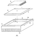
本発明の実施の形態における電子部品200は、図1の断面図に示すように、電子素子20、絶縁部材22及び熱拡散部材24を含んで構成される。絶縁部材22は熱拡散部材24の表面上に搭載され、電子素子20は絶縁部材22の表面上に搭載される。
As shown in the cross-sectional view of FIG. 1, the
電子素子20は、半導体集積回路(IC)、抵抗素子、コンデンサ、インダクタ等を含んで構成される。電子素子20は、電子素子チップをDIPタイプ,SIPタイプ,BGAタイプ等のパッケージに収めることによって構成することができる。本実施の形態における電子部品200は、冷熱サイクル等によって生ずる応力に強いものであるので、例えば、素子の使用時に発熱が大きいIGBTやパワーMOSFET等の大電力用の電子素子を含む場合により効果を発揮することができる。
The
絶縁部材22は、電子素子20と熱拡散部材24との間の電気的な接続を防ぐ部材である。本実施の形態における絶縁部材22は、図2の組立分解図に示すように、短辺L1,長辺L2及び厚さTを有する板状の部材とする。
The insulating
絶縁部材22は、必要とされる絶縁特性、熱伝達率及び機械的な強度を満たしていればどのような材料で構成してもよい。例えば、酸化アルミニウムや窒化アルミニウム等のセラミックから構成することができる。
The insulating
絶縁部材22の表面上に回路層が形成され、回路層に電子素子20のピン20aがハンダ付け等によって接合されて電気的に接続される。回路層は、導電性に優れたアルミニウム、銅、銀、金等の導電性材料によって形成される。また、絶縁部材22と電子素子20との間はハンダ接合、もしくは熱伝導を高めるために、絶縁部材22と電子素子との間に有機ケイ素化合物重合体等のグリース26を塗布して挟み込む構造としてもよい。
A circuit layer is formed on the surface of the insulating
熱拡散部材24は、電子素子20から発生する熱を放散させることによって、電子部品200の温度を下げることを目的にした部材である。放熱器や放熱板と呼ばれることもある。熱拡散部材24は、絶縁部材22よりも線膨張係数が高く、熱伝導率が高いアルミニウムや銅等の金属を材料として形成することが好適である。
The
熱拡散部材24の性能は、熱抵抗によって表される。熱抵抗が小さいほど性能が高く、加えられた熱を効率良く放熱することができる。熱抵抗は、熱拡散部材24の材質、大きさ、形状などによって決定される。熱拡散部材24の熱伝達性能を上げるために表面積が広くなるようにフィン24a等を設けた形状とすることが好適である。熱拡散部材24を冷却する冷媒は空気等の気体であってもよいし、水等の液体であってもよい。また、冷却能力を高めるためにファンやポンプなどを設けて強制的に冷媒によって冷却してもよい。
The performance of the
本実施の形態では、図1の断面図及び図2の組立分解図に示すように、熱拡散部材24の表面に凹み部24bが設けられる。熱拡散部材24の凹み部24b内にハンダ材28を充填し、絶縁部材22の電子素子20が搭載されていない裏面側から、絶縁部材22を凹み部24b内に埋め込むように熱拡散部材24に固定する。このように、ハンダ材28を介して熱拡散部材24に絶縁部材22が搭載される。
In the present embodiment, as shown in the cross-sectional view of FIG. 1 and the exploded view of FIG. 2, a
ハンダ材28は、通常の鉛と錫の合金であるハンダを用いてもよいが、環境に配慮して鉛フリーハンダを用いることも好適である。ハンダ材28は、熱拡散部材24の線膨張係数より小さく、絶縁部材22の線膨張係数よりも大きい線膨張係数を有するものとすることが好適である。
As the
また、凹み部24bの短辺W1及び長辺W2は絶縁部材22の短辺L1及び長辺L2よりもそれぞれ僅かに大きくすることが好適である。このようにすることによって、絶縁部材22を凹み部24b内に配置することができる。また、凹み部24bの深さDは絶縁部材22の厚さTの少なくとも1/4以上とすることが好適である。このように、深さDを絶縁部材22の厚さTの少なくとも1/4以上とし、絶縁部材22の厚さの1/4以上を凹み部24bに埋め込むことが好適である。
Further, it is preferable that the short side W1 and the long side W2 of the
このように熱拡散部材24の凹み部24b内に埋め込むように絶縁部材22を配置することによって、熱拡散部材24と絶縁部材22との線膨張率の違いによる影響を低減することができる。
By disposing the insulating
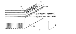
図3は、従来の埋込み型でない積層構造を有する電子部品における熱拡散部材24と絶縁部材22との接合部分における応力の強さをシミュレーションした結果を示す。また、図4は本実施の形態における電子部品200における熱拡散部材24と絶縁部材22との接合部分における応力の強さをシミュレーションした結果を示す。図3及び図4は、ハンダ材28の接合温度である約230℃に電子部品を保持した状態において応力が無いとし、電子部品を0℃に保持した場合における熱応力をシミュレーションした結果を示している。シミュレーションにおいて絶縁部材の線膨張係数は10ppm/Kとし、熱拡散部材の線膨張係数は20ppm/Kに設定した。
FIG. 3 shows the result of simulating the strength of stress at the joint between the
図3及び図4から明らかなように、従来の電子部品よりも本実施の形態の電子部品200において熱拡散部材24と絶縁部材22との間に印加される応力が緩和されていることが分かる。特に、絶縁部材22の角部近傍のように一般的な応力が集中する部分において、従来よりも本実施の形態の電子部品200に加わる応力が小さくなる。具体的には、ハンダ材28に掛る応力は埋め込みなしの場合は−1227MPaであるのに対して、埋め込み有りの場合には−378MPaまで低下している。これは、絶縁部材22が、ハンダ材28を介して埋め込まれたことにより、絶縁部材22の熱変形挙動が熱拡散部材24に追随し易くなり、その結果、主たる熱膨張方向X−Y面にかかる応力が軽減されると共に、凹みハンダ材を介して、側面へ応力が拡散される。さらに、埋め込み構造における各部材間の接合開放端の界面方向が凹み深さ方向Zであるのに対し、Z方向の接合長さは短いため、熱膨張差は小さくなり開放端部での応力集中も起こり難くなったものと考えられる。
As apparent from FIGS. 3 and 4, it can be seen that the stress applied between the
また、絶縁部材22と熱拡散部材24との間に埋め込まれたハンダ材28に生じるクラック30は、図5の概念図に示すように、絶縁部材22や熱拡散部材24の主たる熱膨張方向である平面方向X−Yに対して直交する熱拡散部材24の凹み部24bの深さ方向Zにも延伸する。すなわち、従来の積層構造を有する電子部品では部材間の接合が平面内で行われており、応力に基づくクラック30の伸展方向が応力による部材の伸縮方向と一致してしまっており、本実施の形態では埋め込み構造を採ることによってクラック30の伸展方向をハンダ材28の深さ方向にすることによって平面方向への伸展を抑制できたものと推定される。
Further, the
これにより、絶縁部材22における電子素子20の直下の領域へのクラック30の延伸が抑制され、電子部品200の信頼性を向上できる。特に、絶縁部材22における電子素子20の直下の領域へクラック30が延伸した場合、電子素子20から熱拡散部材24までの熱抵抗が大きくなり、電子素子20の冷却効率が著しく低下するので、それを防ぐことができる点で有利である。
Thereby, the extension of the
また、凹み部24bを設けたことによって、絶縁部材22を熱拡散部材24へ組み込む際の位置合わせ及び保持が容易となる利点もある。
In addition, the provision of the
さらに、ハンダ材28が凹み部24b内に充填されるため、ハンダ材28が熱拡散部材24の表面上にはみ出してしまうことを防ぐこともできる。
Furthermore, since the
<変形例1>
図6に、本発明の実施の形態における変形例の電子部品202の断面図を示す。本変形例では、熱拡散部材24の表面側に凹み部24bを設けるための段差24cを設けている。他の構成については上記実施の形態と同様である。このような構成においても上記実施の形態と同様の作用・効果を得ることができる。
<
FIG. 6 shows a cross-sectional view of an
なお、本変形例では段差24cとしてその枠厚が薄くなったため、平面方向への熱膨張量が小さくなり、熱拡散部材24の熱膨張による絶縁部材22への影響をより小さくすることができる。
In this modification, since the frame thickness of the
<変形例2>
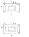
図7に、本発明の実施の形態における変形例の電子部品202の平面図を示す。本変形例では、熱拡散部材24に設けられた凹み部24bの角を曲面状に加工又は逃げ構造に加工している。
<Modification 2>
In FIG. 7, the top view of the
図7(a)では、熱拡散部材24に設けられた凹み部24bの側面同士がつくる角24dを熱拡散部材24の表面側からみて円弧状に加工している。また、図7(b)では、熱拡散部材24に設けられた凹み部24bの角から突出するように半円状の凹み端部24eを設けている。
In FIG. 7A, the
このように、熱拡散部材24に設けられた凹み部24bの角を曲面状に加工又は逃げ構造に加工することによって、熱拡散部材24の凹み部24bの角に掛る応力をより緩和・分散させることができる。なお、凹み部24bの長辺に沿った熱膨張量は短辺に沿った熱膨張量よりも大きいので、図7(b)に示すように、凹み端部24eは凹み部24bの長辺に沿って短辺から突出するように設けることがより好適である。
In this way, by processing the corners of the
なお、本変形例の構成は、上記実施の形態及び変形例1の構成のいずれにも適用することができ、いずれの場合にも熱拡散部材24の凹み部24bの角に掛る応力をより緩和・分散させることができる。
Note that the configuration of the present modification can be applied to both the above-described embodiment and the configuration of
<変形例3>
図8に、本発明の実施の形態における変形例の電子部品206の局所断面図を示す。図8は、絶縁部材22が埋め込まれた凹み部24bを拡大して示した図である。
<Modification 3>
FIG. 8 shows a local cross-sectional view of an
図8(a)は、凹み部24bの底部24fと内側面24gとがつくる隅を曲面状に加工したものである。また、図8(b)は、凹み部24bの内側面24gと表面24hとがつくる隅を曲面状に加工したものである。
FIG. 8A shows a corner formed by the bottom 24f and the
このように、熱拡散部材24に設けられた凹み部24bの角を曲面状に加工することによって、熱拡散部材24の凹み部24bの角に掛る応力をより緩和・分散させることができる。なお、図8(a)及び図8(b)の構成を同時に適用することによって、より高い効果を得ることができる。また、本変形例は、上記実施の形態、変形例1及び2のいずれとも組み合わせ可能である。
In this way, by processing the corners of the
10,20 電子素子、12 絶縁基板、14 熱拡散板、16 応力緩衝部材、20a ピン、22 絶縁部材、24 熱拡散部材、24a フィン、24b 凹み部、24c 段差、24d 角、24e 端部、24f 底部、24g 内側面、24h 表面、26 グリース、28 ハンダ材、30 クラック、100,200,202,206 電子部品。 10, 20 Electronic element, 12 Insulating substrate, 14 Thermal diffusion plate, 16 Stress buffer member, 20a Pin, 22 Insulating member, 24 Thermal diffusion member, 24a Fin, 24b Recessed portion, 24c Step, 24d square, 24e End, 24f Bottom, 24g inner surface, 24h surface, 26 grease, 28 solder material, 30 cracks, 100, 200, 202, 206 electronic components.
Claims (4)
前記第1部材の熱膨張係数は前記第2部材の熱膨張係数よりも小さく、
前記第2部材の表面に設けられた凹み部内に前記第1部材が埋め込まれるように搭載され、
前記凹み部は、前記第2部材の表面から突出する段差部に設けられ、
前記凹み部の角が曲面状に加工されていることを特徴とする電子部品。 An electronic component comprising: a first member on which an electronic element is mounted; and a second member on which the first member is mounted;
The thermal expansion coefficient of the first member is smaller than the thermal expansion coefficient of the second member,
It is mounted so that the first member is embedded in a recess provided on the surface of the second member ,
The recess is provided in a stepped portion protruding from the surface of the second member,
An electronic component, wherein a corner of the recess is processed into a curved surface .
前記第1部材の熱膨張係数は前記第2部材の熱膨張係数よりも小さく、
前記第2部材の表面に設けられた凹み部内に前記第1部材が埋め込まれるように搭載され、
前記凹み部は、前記第2部材の表面から突出する段差部に設けられ、
前記凹み部の角は逃げ構造に加工されていることを特徴とする電子部品。 An electronic component comprising: a first member on which an electronic element is mounted; and a second member on which the first member is mounted;
The thermal expansion coefficient of the first member is smaller than the thermal expansion coefficient of the second member,
It is mounted so that the first member is embedded in a recess provided on the surface of the second member,
The recess is provided in a stepped portion protruding from the surface of the second member,
An electronic component characterized in that corners of the recess are processed into a relief structure .
前記凹み部の深さは、前記第1部材の厚さの1/4以上であることを特徴とする電子部品。 The electronic component according to claim 1 or 2,
The depth of the said recessed part is 1/4 or more of the thickness of a said 1st member, The electronic component characterized by the above-mentioned.
前記第1部材及び前記第2部材は、前記凹み部に充填されたハンダ材で固着されていることを特徴とする電子部品。
The electronic component according to any one of claims 1 to 3 ,
The electronic component, wherein the first member and the second member are fixed with a solder material filled in the recess.
Priority Applications (3)
| Application Number | Priority Date | Filing Date | Title |
|---|---|---|---|
| JP2008122368A JP4989552B2 (en) | 2008-05-08 | 2008-05-08 | Electronic components |
| US12/436,976 US8446727B2 (en) | 2008-05-08 | 2009-05-07 | Electronic component |
| CN200910138567.4A CN101577257B (en) | 2008-05-08 | 2009-05-08 | Electronic component |
Applications Claiming Priority (1)
| Application Number | Priority Date | Filing Date | Title |
|---|---|---|---|
| JP2008122368A JP4989552B2 (en) | 2008-05-08 | 2008-05-08 | Electronic components |
Publications (2)
| Publication Number | Publication Date |
|---|---|
| JP2009272487A JP2009272487A (en) | 2009-11-19 |
| JP4989552B2 true JP4989552B2 (en) | 2012-08-01 |
Family
ID=41266715
Family Applications (1)
| Application Number | Title | Priority Date | Filing Date |
|---|---|---|---|
| JP2008122368A Expired - Fee Related JP4989552B2 (en) | 2008-05-08 | 2008-05-08 | Electronic components |
Country Status (3)
| Country | Link |
|---|---|
| US (1) | US8446727B2 (en) |
| JP (1) | JP4989552B2 (en) |
| CN (1) | CN101577257B (en) |
Families Citing this family (11)
| Publication number | Priority date | Publication date | Assignee | Title |
|---|---|---|---|---|
| JP5949213B2 (en) * | 2012-06-28 | 2016-07-06 | セイコーエプソン株式会社 | Shift register circuit, electro-optical device, and electronic apparatus |
| JP5673627B2 (en) * | 2012-08-03 | 2015-02-18 | トヨタ自動車株式会社 | Semiconductor device and manufacturing method thereof |
| DE102012222959B4 (en) * | 2012-12-12 | 2015-04-02 | Semikron Elektronik Gmbh & Co. Kg | Power component device |
| JP6138500B2 (en) * | 2013-01-30 | 2017-05-31 | 株式会社 日立パワーデバイス | Power semiconductor device |
| WO2015080161A1 (en) * | 2013-11-29 | 2015-06-04 | 株式会社神戸製鋼所 | Base plate, and semiconductor device provided with base plate |
| JP6409846B2 (en) * | 2016-10-18 | 2018-10-24 | トヨタ自動車株式会社 | Semiconductor device |
| JP2018157201A (en) * | 2017-03-16 | 2018-10-04 | 三菱マテリアル株式会社 | Resistance device and method of manufacturing resistance device |
| JP7031172B2 (en) * | 2017-08-24 | 2022-03-08 | 富士電機株式会社 | Semiconductor device |
| EP3817041B1 (en) * | 2018-06-26 | 2023-08-16 | Kyocera Corporation | Electronic element mounting substrate, electronic device, and electronic module |
| CN110488886B (en) * | 2019-08-29 | 2020-12-15 | 中国科学院国家天文台 | A kind of electronic device working temperature control method and device |
| CN116364666A (en) * | 2023-02-03 | 2023-06-30 | 江苏宏微科技股份有限公司 | Power module packaging structure |
Family Cites Families (32)
| Publication number | Priority date | Publication date | Assignee | Title |
|---|---|---|---|---|
| US4012832A (en) * | 1976-03-12 | 1977-03-22 | Sperry Rand Corporation | Method for non-destructive removal of semiconductor devices |
| US4092697A (en) * | 1976-12-06 | 1978-05-30 | International Business Machines Corporation | Heat transfer mechanism for integrated circuit package |
| JPS577989A (en) * | 1980-06-17 | 1982-01-16 | Matsushita Electric Ind Co Ltd | Mount for semiconductor laser |
| JPS6420645A (en) * | 1987-07-15 | 1989-01-24 | Mitsubishi Electric Corp | Semiconductor device |
| JP2697229B2 (en) | 1990-02-27 | 1998-01-14 | 三菱電機株式会社 | Heat dissipation metal plate |
| US5137836A (en) * | 1991-05-23 | 1992-08-11 | Atmel Corporation | Method of manufacturing a repairable multi-chip module |
| US5168926A (en) * | 1991-09-25 | 1992-12-08 | Intel Corporation | Heat sink design integrating interface material |
| JPH0562048U (en) | 1992-01-24 | 1993-08-13 | 日本電子機器株式会社 | Power element fixing structure |
| US5268814A (en) * | 1992-05-20 | 1993-12-07 | International Business Machines Corporation | Module packaging |
| US5396403A (en) * | 1993-07-06 | 1995-03-07 | Hewlett-Packard Company | Heat sink assembly with thermally-conductive plate for a plurality of integrated circuits on a substrate |
| JPH07312474A (en) | 1994-05-18 | 1995-11-28 | Toyota Autom Loom Works Ltd | Electronic component mounting structure |
| US5663106A (en) * | 1994-05-19 | 1997-09-02 | Tessera, Inc. | Method of encapsulating die and chip carrier |
| US5642262A (en) * | 1995-02-23 | 1997-06-24 | Altera Corporation | High-density programmable logic device in a multi-chip module package with improved interconnect scheme |
| US6578263B2 (en) * | 1996-06-04 | 2003-06-17 | Yazaki Corporation | Method of manufacturing a wire harness |
| US5932925A (en) * | 1996-09-09 | 1999-08-03 | Intricast, Inc. | Adjustable-pressure mount heatsink system |
| JP4427154B2 (en) | 2000-03-14 | 2010-03-03 | 株式会社東芝 | Ceramic circuit board |
| JP2002043479A (en) * | 2000-07-26 | 2002-02-08 | Hitachi Ltd | Semiconductor device |
| JP2002043480A (en) * | 2000-07-26 | 2002-02-08 | Hitachi Ltd | Semiconductor device |
| JP3923258B2 (en) * | 2001-01-17 | 2007-05-30 | 松下電器産業株式会社 | Power control system electronic circuit device and manufacturing method thereof |
| JP2002217346A (en) * | 2001-01-19 | 2002-08-02 | Toyota Motor Corp | Electronic element chip module |
| US6573592B2 (en) * | 2001-08-21 | 2003-06-03 | Micron Technology, Inc. | Semiconductor die packages with standard ball grid array footprint and method for assembling the same |
| US6752204B2 (en) * | 2001-09-18 | 2004-06-22 | Intel Corporation | Iodine-containing thermal interface material |
| US6758263B2 (en) * | 2001-12-13 | 2004-07-06 | Advanced Energy Technology Inc. | Heat dissipating component using high conducting inserts |
| US6757170B2 (en) * | 2002-07-26 | 2004-06-29 | Intel Corporation | Heat sink and package surface design |
| US7173334B2 (en) * | 2002-10-11 | 2007-02-06 | Chien-Min Sung | Diamond composite heat spreader and associated methods |
| US7057277B2 (en) * | 2003-04-22 | 2006-06-06 | Industrial Technology Research Institute | Chip package structure |
| US6816378B1 (en) * | 2003-04-28 | 2004-11-09 | Hewlett-Packard Development Company, L.P. | Stack up assembly |
| JP4621531B2 (en) | 2005-04-06 | 2011-01-26 | 株式会社豊田自動織機 | Heat dissipation device |
| US7787570B2 (en) * | 2005-07-13 | 2010-08-31 | Skyworks Solutions, Inc. | Polar loop radio frequency (RF) transmitter having increased dynamic range amplitude control |
| CN101026133A (en) * | 2006-02-24 | 2007-08-29 | 日月光半导体制造股份有限公司 | Semiconductor package structure with heat sink and manufacturing method thereof |
| CN2894066Y (en) * | 2006-03-09 | 2007-04-25 | 黄敬党 | Voltage frequency converter |
| KR101463075B1 (en) * | 2008-02-04 | 2014-11-20 | 페어차일드코리아반도체 주식회사 | Heat sink package |
-
2008
- 2008-05-08 JP JP2008122368A patent/JP4989552B2/en not_active Expired - Fee Related
-
2009
- 2009-05-07 US US12/436,976 patent/US8446727B2/en not_active Expired - Fee Related
- 2009-05-08 CN CN200910138567.4A patent/CN101577257B/en not_active Expired - Fee Related
Also Published As
| Publication number | Publication date |
|---|---|
| CN101577257B (en) | 2014-09-17 |
| JP2009272487A (en) | 2009-11-19 |
| US20090279276A1 (en) | 2009-11-12 |
| US8446727B2 (en) | 2013-05-21 |
| CN101577257A (en) | 2009-11-11 |
Similar Documents
| Publication | Publication Date | Title |
|---|---|---|
| JP4989552B2 (en) | Electronic components | |
| TWI620289B (en) | Substrate with heat sink power module, substrate for cooling power module and power module | |
| JP4207896B2 (en) | Semiconductor device | |
| CN109314063B (en) | Power semiconductor device | |
| CN100390977C (en) | Semiconductor device and its manufacturing method | |
| CN107078115B (en) | semiconductor module | |
| CN101789404A (en) | Heat radiator | |
| WO2015046040A1 (en) | Crimped heat sink and power module with integrated heat sink | |
| JPWO2017221730A1 (en) | Power semiconductor device and method for manufacturing power semiconductor device | |
| JP2009283741A (en) | Semiconductor device | |
| JP4683043B2 (en) | Manufacturing method of semiconductor device | |
| JP7237647B2 (en) | Circuit boards and electronic devices | |
| JP5222838B2 (en) | Control device | |
| KR20180059778A (en) | A substrate for a light emitting module, a light emitting module, a substrate for a light emitting module formed with a cooler, and a method for manufacturing a substrate for a light emitting module | |
| JP2004356625A (en) | Semiconductor device and manufacturing method thereof | |
| CN100385652C (en) | Semiconductor device with a plurality of semiconductor chips | |
| JP2009200258A (en) | Semiconductor module | |
| WO2019163941A1 (en) | Substrate for power modules, and power module | |
| JP2007142097A (en) | Semiconductor device | |
| JP6992913B2 (en) | Lead frame wiring structure and semiconductor module | |
| CN1835223B (en) | Semiconductor device and insulating substrate for the semiconductor device | |
| JP2004343035A (en) | Heat dissipation components, circuit boards and semiconductor devices | |
| JP2007012725A (en) | Semiconductor device | |
| KR102930091B1 (en) | Semiconductor package | |
| WO2014045711A1 (en) | Semiconductor module |
Legal Events
| Date | Code | Title | Description |
|---|---|---|---|
| A621 | Written request for application examination |
Free format text: JAPANESE INTERMEDIATE CODE: A621 Effective date: 20110221 |
|
| A977 | Report on retrieval |
Free format text: JAPANESE INTERMEDIATE CODE: A971007 Effective date: 20120209 |
|
| A131 | Notification of reasons for refusal |
Free format text: JAPANESE INTERMEDIATE CODE: A131 Effective date: 20120214 |
|
| A521 | Request for written amendment filed |
Free format text: JAPANESE INTERMEDIATE CODE: A523 Effective date: 20120323 |
|
| TRDD | Decision of grant or rejection written | ||
| A01 | Written decision to grant a patent or to grant a registration (utility model) |
Free format text: JAPANESE INTERMEDIATE CODE: A01 Effective date: 20120410 |
|
| A01 | Written decision to grant a patent or to grant a registration (utility model) |
Free format text: JAPANESE INTERMEDIATE CODE: A01 |
|
| A61 | First payment of annual fees (during grant procedure) |
Free format text: JAPANESE INTERMEDIATE CODE: A61 Effective date: 20120427 |
|
| FPAY | Renewal fee payment (event date is renewal date of database) |
Free format text: PAYMENT UNTIL: 20150511 Year of fee payment: 3 |
|
| R250 | Receipt of annual fees |
Free format text: JAPANESE INTERMEDIATE CODE: R250 |
|
| R250 | Receipt of annual fees |
Free format text: JAPANESE INTERMEDIATE CODE: R250 |
|
| R250 | Receipt of annual fees |
Free format text: JAPANESE INTERMEDIATE CODE: R250 |
|
| LAPS | Cancellation because of no payment of annual fees |