JP4989461B2 - Elastic wave touch screen - Google Patents
Elastic wave touch screen Download PDFInfo
- Publication number
- JP4989461B2 JP4989461B2 JP2007508575A JP2007508575A JP4989461B2 JP 4989461 B2 JP4989461 B2 JP 4989461B2 JP 2007508575 A JP2007508575 A JP 2007508575A JP 2007508575 A JP2007508575 A JP 2007508575A JP 4989461 B2 JP4989461 B2 JP 4989461B2
- Authority
- JP
- Japan
- Prior art keywords
- substrate
- touch sensor
- transducer
- conductive layer
- layer
- Prior art date
- Legal status (The legal status is an assumption and is not a legal conclusion. Google has not performed a legal analysis and makes no representation as to the accuracy of the status listed.)
- Expired - Fee Related
Links
Images


Classifications
-
- G—PHYSICS
- G06—COMPUTING; CALCULATING OR COUNTING
- G06F—ELECTRIC DIGITAL DATA PROCESSING
- G06F3/00—Input arrangements for transferring data to be processed into a form capable of being handled by the computer; Output arrangements for transferring data from processing unit to output unit, e.g. interface arrangements
- G06F3/01—Input arrangements or combined input and output arrangements for interaction between user and computer
- G06F3/03—Arrangements for converting the position or the displacement of a member into a coded form
- G06F3/041—Digitisers, e.g. for touch screens or touch pads, characterised by the transducing means
- G06F3/043—Digitisers, e.g. for touch screens or touch pads, characterised by the transducing means using propagating acoustic waves
- G06F3/0436—Digitisers, e.g. for touch screens or touch pads, characterised by the transducing means using propagating acoustic waves in which generating transducers and detecting transducers are attached to a single acoustic waves transmission substrate
Description
本発明はタッチセンサーに関する。より詳細には、本発明は、機能性を有する狭いボーダーおよび感度が増加したタッチ検知エリアを備えた弾性波タッチセンサーおよび弾性波タッチスクリーンに関する。 The present invention relates to a touch sensor. More particularly, the present invention relates to an elastic wave touch sensor and an elastic wave touch screen having a narrow border having functionality and a touch detection area with increased sensitivity.
弾性波タッチセンサーは、タッチセンサー基板を横切って伝搬(または伝播)する弾性波に加えられるタッチ効果に起因してタッチの存在および位置を検知できるタッチ検知エリアを備えている。かかる弾性波タッチセンサーは、レイリー波(擬似レイリー波を含む)、ラム波、剪断波、または種々の弾性波の組合せを用いている。 The elastic wave touch sensor includes a touch detection area that can detect the presence and position of a touch due to a touch effect applied to an elastic wave that propagates (or propagates) across the touch sensor substrate. Such an elastic wave touch sensor uses a Rayleigh wave (including a pseudo Rayleigh wave), a Lamb wave, a shear wave, or a combination of various elastic waves.
図1は、従来の弾性波タッチセンサー、弾性波タッチスクリーン1の作動形態を示している。タッチスクリーン1は、タッチされた二次元座標の位置を決めるタッチ検知エリア2を有している。例えば、タッチ検知エリア2は、点線16(ベゼル10の内側境界を表している点線)によって境界付けられたエリアを含んでいる。第1送信トランスデューサー3aは、タッチ検知エリア2の外側に配置されており、弾性波を伝えるようにタッチスクリーン1の表面に連結されている。第1送信トランスデューサー3aによって、タッチスクリーン1の上端にて平行に伝搬するように(一般的にはタッチスクリーン1の面にて伝搬するように)弾性波信号が弾性波11aの形態で送られる。弾性波11aの伝搬経路には、部分反射弾性波要素4の第1直線状アレイ13aが配置されている。弾性波要素4の各々は、弾性波信号を(約90°の角度で)部分的に反射させて送信しており、それによって、タッチ検知エリア2を垂直に伝搬する複数の弾性波(例えば、5a,5bおよび5c)が生じることになる。反射要素4の間隔は、弾性波信号の減衰が補われるように、第1トランスミッター3aからの離れるほど変化している。反射要素4が一様に離隔している場合であっても、反射要素4の反射強度を変えることによって信号を均一化することができる。弾性波5a,5bおよび5cは、部分弾性反射要素4の第2直線状アレイ13bによって再度反射して、第1受信トランスデューサー6aの方向に向かって略90°(矢印11bで示される方向)に方向を変える。そして、第1受信トランスデューサー6aによって弾性波5a、5bおよび5cが検知された後、電気信号に変換されてデータ処理される。このような構成と同様の構成は、タッチスクリーン1の左側エッジおよび右側エッジに沿うように設けられている。第2送信トランスデューサー3bは、右側エッジに沿うように弾性波12aを発生させる。弾性波反射要素4の第3直線状アレイ13cによって、弾性波12aは、タッチ検知エリア2を水平方向(X軸と平行)に横切って進行する複数の弾性波(例えば7a、7bおよび7c)にされる。弾性波7a、7bおよび7cは、弾性波反射要素4の第4直線状アレイ13dによって、受信トランスデューサー6bの方向(矢印12bの方向)へと向きを変えられる。そして、受信トランスデューサー6bでは弾性波7a、7bおよび7cが検知され、電気信号に変換されることになる。
FIG. 1 shows an operation mode of a conventional acoustic wave touch sensor and acoustic
タッチ検知エリア2では、指またはスタイラス等の物体によって参照番号8で示す位置がタッチされると、弾性波5bおよび7aのエネルギーの幾らかがタッチした物体によって吸収される。その結果、減衰が生じ、受信トランスデューサー6a、6bにおいて、弾性波信号の変動(または摂動)が検知される。マイクロプロセッサー(図示せず)を用いてデータの時間遅れを解析すると、タッチされた位置8の座標を決定することができる。図1のデバイスは、送信トランスデューサーおよび受信トランスデューサーと2種類のトランスデューサーを用いたタッチスクリーンとして機能し得る。
In the
図1の点線で表されているハウジング9は、タッチスクリーン1と関連を有するものである。このハウジングは、例えば成形ポリマーまたはシート材料などの適当な材料から形成することができる。ハウジング9には、ベゼル10(図1ではベゼルの内側輪郭を点線16で表し、ベゼルの外側輪郭を点線17で示している)が含まれている。内側点線16によって、ハウジング9とタッチスクリーン1の外周部との重なりが表されている。ハウジング9によって、送信トランスデューサー、受信トランスデューサーおよび他の要素を外から見えないように隠すことができる一方、タッチ検知エリア2を露出させることができる。このような構成では、隠された要素が汚染および/または損傷から保護されることになる。また、美的外観が供されると共にユーザーのためのタッチ検知エリアが規定される。
A housing 9 represented by a dotted line in FIG. 1 is related to the
タッチスクリーンは、ディスプレイ・パネル上に設けられた別個のフェースプレートを有し成る。フェースプレートは典型的にはガラスから形成されるものの、他のいずれの適当な基板を用いてもよい。ディスプレイ・パネルは、陰極線管(CRT)、液晶ディスプレイ(LCD)、プラズマ・ディスプレイ、エレクトロルミネセント・ディスプレイ(または電子発光ディスプレイ)もしくは有機発光ダイオード・ディスプレイ(OLEDディスプレイ)であってよく、あるいは他の種類のディスプレイであってもよい。 The touch screen comprises a separate face plate provided on the display panel. The faceplate is typically formed from glass, but any other suitable substrate may be used. The display panel may be a cathode ray tube (CRT), liquid crystal display (LCD), plasma display, electroluminescent display (or electroluminescent display) or organic light emitting diode display (OLED display), or other It may be a type of display.
図1に示すように、タッチ検知エリア2は、ボーダー領域15によって包囲されている。尚、このボーダー領域15には、反射要素4、送信トランスデューサー3aおよび受信トランスデューサー3bが配置されている。ボーダー領域15の幅が減少すると、タッチ検知エリア2が増加することになる。タッチスクリーン等の透明タッチセンサーを用いたタッチセンサー用途では、ボーダーの幅が特に重要となる。タッチセンサーのボーダー領域15がより狭いと、表示画像の周囲のボーダー部が狭い表示モニターに対してタッチセンサーを組み込むことができる。このような特徴は、モニター等のデバイスがしゃれたデザインを有し、機械的にコンパクトなデザインを有するものが一般的な傾向となってきている点を踏まえると、望ましいといえる。また、ボーダー領域15がより狭いタッチセンサーは、より容易に封止できるだけでなく、より軽量であり、より多くの検知エリアを有している。競合するタッチスクリーン技術(例えば弾性波タッチスクリーン技術、容量式タッチスクリーン技術、抵抗式タッチスクリーン技術および赤外式タッチスクリーン技術など)の中でも、弾性波タッチスクリーンは、より広いボーダー部を有するといえる。
As shown in FIG. 1, the
弾性波タッチセンサーの基板の上方に位置するタッチ検知面に対して、弾性波の実質的な送信および受信を行うトランスデューサーを設けることは既知である。弾性波に対しては、反射アレイを組み込むことに代えて、トランスミッター−検出器から成る経路を用いてタッチセンサーのタッチ検知領域を横切るように弾性波を方向付けることができるものの、多くのトランスデューサーを用いる必要がある。用いられるトランスデューサーは、タッチ面に設けられるウエッジ・トランスデューサー(wedge tranducer)であるので、それによって貴重なボーダー・スペースが占有されてしまうことになる。米国特許第6756973号に開示されているように、櫛歯型トランスデューサーを用いて、反射アレイを用いないタッチスクリーンを設計することもできる(米国特許第6756973号の開示内容は引用することにより本明細書に組み込まれる)。米国特許第6756973号に開示されている櫛歯型トランスデューサーは、タッチスクリーンの上面に配置されるので、それによって貴重なボーダー・スペースが占有されてしまう。これまでのところ、幾つかのトランスデューサーおよび反射アレイを用いて弾性波をタッチセンサーを通過するように方向付けるタッチセンサーでは、タッチ検知領域と同じ基板面のボーダーにアレイが配置されているので、それによってボーダー・スペースが占有されている。 It is known to provide a transducer for substantially transmitting and receiving elastic waves to a touch detection surface located above the substrate of the elastic wave touch sensor. For acoustic waves, instead of incorporating a reflective array, a transducer-detector path can be used to direct the acoustic wave across the touch sensing area of the touch sensor, but many transducers Must be used. The transducer used is a wedge transducer provided on the touch surface, thereby occupying valuable border space. As disclosed in US Pat. No. 6,756,973, a touch screen without a reflective array can also be designed using a comb-type transducer (the disclosure of US Pat. No. 6,756,973 is incorporated herein by reference). Incorporated in the description). The comb-shaped transducer disclosed in US Pat. No. 6,756,973 is placed on the top surface of the touch screen, thereby occupying valuable border space. So far, in touch sensors that use several transducers and reflective arrays to direct elastic waves through the touch sensor, the array is located on the same board surface border as the touch sensing area, This occupies border space.
弾性波を送信および受信するトランスデューサーを弾性波タッチセンサーの基板の側壁に設けることも既知である。そのような場合でも、反射アレイをタッチ面に配置しなければならないので、それによって貴重なボーダー・スペースが占有されてしまう。 It is also known to provide a transducer for transmitting and receiving elastic waves on the side wall of the substrate of the elastic wave touch sensor. Even in such a case, the reflective array must be placed on the touch surface, thereby occupying valuable border space.
米国特許第6636201号(その内容は引用することによって本明細書に組み込まれる)に記載されているように、ボーダー領域に弾性波を集めるべく導波路を用いてタッチスクリーンのボーダー領域を減少させることは可能である。しかしながら、タッチセンサー基板のタッチ表面に導波路を設けなくても済むような別の解決策が望まれている。 Reducing the border area of a touch screen using a waveguide to collect elastic waves in the border area, as described in US Pat. No. 6,636,201, the contents of which are incorporated herein by reference. Is possible. However, another solution is desired that eliminates the need to provide a waveguide on the touch surface of the touch sensor substrate.
タッチセンサーのボーダー領域を減じることに加えて、タッチセンサーをできる限りフラットにすることが望ましい。このことは、タッチセンサーをLCDパネルと一体化してタッチスクリーンを製作できる点で特に有利となる。タッチセンサーが非常にフラットでLCDパネルと平行となっている場合には、タッチセンサーとLCDパネルとを容易に組み合わせることができ、それによって、封止を容易に行えるコンパクトなシステムを構築できる。タッチセンサーが嵩高いベゼルおよびボーダー領域を有していると、LCDパネルとタッチセンサーとの間の封止は複雑になる。 In addition to reducing the border area of the touch sensor, it is desirable to make the touch sensor as flat as possible. This is particularly advantageous in that the touch sensor can be integrated with the LCD panel to produce a touch screen. If the touch sensor is very flat and parallel to the LCD panel, the touch sensor and the LCD panel can be easily combined, thereby creating a compact system that can be easily sealed. If the touch sensor has a bulky bezel and border area, the sealing between the LCD panel and the touch sensor becomes complicated.
上述のような理由から、ボーダー領域が非常に狭くなった新しい弾性波タッチセンサー設計が望まれている。更に、センサーがフラットで、平面状デバイス(例えばLCDモニター)と容易に一体化できて封止できる新しい弾性波タッチセンサー設計も望まれている。 For the above reasons, a new elastic wave touch sensor design with a very narrow border area is desired. There is also a need for a new acoustic wave touch sensor design that is flat and can be easily integrated and sealed with planar devices (eg, LCD monitors).
ある態様では、タッチセンサーは、弾性波を伝搬させることが可能な基板を有して成る。基板は、タッチ検知領域を有する第1面、および、第1面と第1エッジにて交差している第1側壁を含んでいる。基板の第1側壁には、トランスミッターが設けられている。トランスミッターは、第1側壁から直接的に伝搬する弾性波を発生させる。かかる弾性波が、タッチ検知領域の少なくとも一部を通過する。 In one embodiment, the touch sensor includes a substrate capable of propagating elastic waves. The substrate includes a first surface having a touch detection area, and a first side wall intersecting the first surface at a first edge. A transmitter is provided on the first side wall of the substrate. The transmitter generates an elastic wave that propagates directly from the first sidewall. Such elastic waves pass through at least a part of the touch detection area.
別の態様では、タッチセンサー・システムは、弾性波を伝搬させることが可能な基板を有して成る。基板は、タッチ検知領域を有する第1面を含んでいる。第1側壁および第2側壁は第1面と交差している。基板の第1側壁にはトランスミッターが設けられている。トランスミッターは第1側壁から直接的に伝搬する弾性波を発生させており、かかる弾性波がタッチ検知領域の少なくとも一部を横切るように伝搬する。基板の第2側壁には検出器が設けられており、それによって、タッチ検知領域の少なくとも一部を横断した後の弾性波が検出されることになる。 In another aspect, the touch sensor system comprises a substrate capable of propagating elastic waves. The substrate includes a first surface having a touch detection area. The first side wall and the second side wall intersect the first surface. A transmitter is provided on the first side wall of the substrate. The transmitter generates an elastic wave that propagates directly from the first side wall, and the elastic wave propagates across at least a part of the touch detection area. A detector is provided on the second side wall of the substrate, whereby the elastic wave after crossing at least a part of the touch detection area is detected.
別の態様として、弾性波を伝搬させることが可能な基板のタッチ検知領域に対して行われたタッチを検出する方法が供される。この方法に用いられる基板は、タッチ検知領域を有する第1面、および、その第1面と交差している第1側壁および第2側壁を含んでいる。かかる方法では、基板の第1側壁の近傍において弾性波を発生させる。弾性波が基板の第1側壁の一部を通るように基板を伝搬した後、タッチ検知領域の少なくとも一部を横切るように、弾性波を方向付ける。その後、弾性波を基板の第2側壁の近傍で検出する。 As another aspect, a method for detecting a touch performed on a touch detection region of a substrate capable of propagating an elastic wave is provided. A substrate used in this method includes a first surface having a touch detection area, and first and second sidewalls intersecting the first surface. In such a method, an elastic wave is generated in the vicinity of the first side wall of the substrate. After the elastic wave propagates through the substrate so as to pass through a part of the first side wall of the substrate, the elastic wave is directed so as to cross at least a part of the touch detection area. Thereafter, an elastic wave is detected in the vicinity of the second side wall of the substrate.
別の態様では、タッチセンサーは、弾性波を伝搬させることが可能な基板を有して成る。基板は、タッチ検知領域を有する第1面を含んでいる。基板にはトランスデューサーが形成されている。トランスデューサーは、基板に形成された後で熱硬化に付された圧電素子を有して成る。トランスデューサーは、弾性波の発生または弾性波の検出の少なくとも一方を行うように構成されている。 In another aspect, the touch sensor includes a substrate capable of propagating elastic waves. The substrate includes a first surface having a touch detection area. A transducer is formed on the substrate. The transducer comprises a piezoelectric element that is formed on a substrate and then subjected to thermosetting. The transducer is configured to perform at least one of generation of elastic waves and detection of elastic waves.
別の態様では、タッチセンサーは、弾性波を伝搬させることが可能な基板を有して成る。基板は、タッチ検知領域を有する第1面を含んでいる。トランスデューサーは、弾性波の発生または受信の少なくとも一方を行うように構成されている。トランスデューサーは、圧電材料を含んで成るストリップを含んでいる。ストリップは基板に取り付けられている。 In another aspect, the touch sensor includes a substrate capable of propagating elastic waves. The substrate includes a first surface having a touch detection area. The transducer is configured to generate and / or receive elastic waves. The transducer includes a strip comprising a piezoelectric material. The strip is attached to the substrate.
別の態様では、タッチセンサー基板上にトランスデューサーを形成する方法が供される。この方法で用いられる基板は、タッチ検知領域を有する第1面を含んでいる。かかる方法では、基板に導電層を供する(または形成する)。第1導電層の少なくとも一部が被われるように圧電層を基板に供する(第1導電層の少なくとも一部が圧電層によって被われる)。圧電層は、基板に供給された後で熱硬化に付す。 In another aspect, a method is provided for forming a transducer on a touch sensor substrate. The substrate used in this method includes a first surface having a touch detection area. In such a method, a conductive layer is provided (or formed) on the substrate. The piezoelectric layer is provided on the substrate so that at least part of the first conductive layer is covered (at least part of the first conductive layer is covered by the piezoelectric layer). The piezoelectric layer is subjected to heat curing after being supplied to the substrate.
上述した記載および以下で行う本発明の或る態様についての詳細な説明は、図面を参照することによって、より理解が深まるであろう。尚、本発明は、図面に示す構成および手段に制限されないことを理解されよう。 The foregoing description and the following detailed description of certain aspects of the present invention will become better understood with reference to the drawings. It will be understood that the present invention is not limited to the arrangements and instrumentality shown in the drawings.
図1に示すような従来の反射アレイは、約9〜26個の弾性波波長に相当する約5mm〜15mmの幅を有している(約5MHzの常套の周波数が約0.57mmの波長に相当すると仮定している)。より幅の狭い反射アレイは典型的にはより小さいスクリーンに用いられる。 The conventional reflective array as shown in FIG. 1 has a width of about 5 mm to 15 mm corresponding to about 9 to 26 elastic wave wavelengths (a conventional frequency of about 5 MHz has a wavelength of about 0.57 mm). Assumed to be equivalent). Narrower reflective arrays are typically used for smaller screens.
図2は、本発明の態様に従って、タッチ面24、エッジ22および側壁32を有するタッチセンサー基板20を示している。基板の対向するエッジ26は、基板20の第2面28に相当する面と各々の側壁32に相当する面とが交差する箇所に形成されている。基板20の形成には、ガラス、セラミックおよび金属(例えばアルミニウムまたはスチール)等の適当な材料を用いてもよい。ある用途では、弾性波の損失が少ないガラスが望ましくなる。例えば、ホウケイ酸ガラスは、損失が少なく、受信された信号振幅が増加し得るので、タッチセンサー・エリアをより大きくすることが可能となる。
FIG. 2 illustrates a
側壁32がタッチ面24と当接する箇所に形成される角度42および角度44は90°であるか、あるいは20°〜90°となっており、側壁32がタッチ面24に対して垂直または実質的に垂直となっている。側壁32は実質的に欠陥のないように又は無きずで(free of defect)形成されており、欠けあと(chip)、筋状部(striation)、凹み、不均一領域など、側壁32におけるデビエーション部(またはズレをもたらす部分、deviation)が、弾性波波長(例えばレイリー波の波長)よりも短い寸法を有しており、好ましくは、レイリー波の波長の20%未満の寸法を有している。
The
クリーンな側壁(clean sidewall)32は、基板20の形成に用いる材料に適した方法で形成することができる。例えば、ガラスを切断および機械加工してクリーンな側壁32を得ることができる。場合によっては、慎重に実施できるのであれば、ガラスをけがき折断してよく、それによって、けがき折断された面の反対側にクリーンな側壁32を形成することができる。別法にて、例えば局所的なレーザー加熱法およびガス噴射による冷却法を用いた熱応力で割れ目(または裂け目、fracture)を制御して更に進行させることによって、クリーンな側壁32を形成してもよい。更に、エッジ22を、クリーンな側壁32と同様に実質的に欠陥のないように形成してもよい。
The
図3は、本発明の態様に従って弾性波発生または弾性波検出を行う機構52〜58を側壁32に備えたタッチセンサー50を示している。側壁32は、分かりやすくするために側壁34〜40として表している。タッチセンサー50は、タッチ検知面24を有する基板20を有して成る。側壁34〜40に対してそれぞれ配置された機構52〜58は、各々、弾性波の発生および/または検出を行う。それゆえ、基板20のタッチ面24に反射アレイなどの機構を形成する必要がない。場合によっては、各々の機構52〜58が、基板20を超えて延在するようなタブ(tab)60〜66を有しており、電気接続が行われる。
FIG. 3 shows a touch sensor 50 having mechanisms 52-58 on the
例えば、機構52および機構56の2つは弾性波を発生させることができる一方、機構54および58の2つは弾性波を検出することできる。機構52および機構56は、矩形基板20の一方の対角線に略平行な方向(矢印71で示すような方向)に進行する弾性波(例えばバルク剪断波)を形成する。
For example, two of
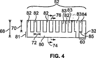
図4は、本発明の態様に従って、側壁32に形成された弾性波発生または弾性波受信を行う機構52を示している。第1導電層または第1電極84が側壁32に形成されている。第1電極84は、側壁32の面を全体的又は略全体的に被うように形成され得る。第1電極84上には、圧電材料83の層(例えば、圧電ポリマー・フィルムまたは焼成圧電セラミック材料)が適用される。例えばタブ60などにおいて電気接続が可能となるように、第1電極84の一部85は、圧電層83を超えるように延在していてもよい。基礎部81およびそれから延在する周期的に連続する構造(例えばフィンガー82)を備えた第2電極80は、圧電層83上にて側壁32に沿うように配置されている。第2電極80は、銅などの材料から形成され得る。フィンガー(finger)82は、弾性波を所望の方向にコヒーレントに(または干渉作用で、coherently)発生または受信するトランスミッターまたはレシーバーのアレイ(位相合わせされたアレイ)として機能する。別法にて、図4に示す機構52を、基板20とは別個に形成されるピエゾ・ストリップ(または細長いピエゾ、piezo strip)として形成してもよい。そのようなピエゾ・ストリップは、以下にて説明する図9のピエゾ・ストリップと同様のピエゾ・ストリップ12〜14であり得る。
FIG. 4 illustrates a
機構52を用いて、剪断波、ラム波またはレイリー波を発生させたり、または、それらを受信したりしてもよい。第1電極84をアース接続し、振動電圧(図示せず)を第2電極に加えてもよい。剪断波を使用した態様について、以下にてより詳細に説明する。剪断波が用いられる場合、フィンガー82の長さ70が側壁32の高さ方向(側壁高さの略全体を占めるように)または基板20の深さ60方向に延在して基礎部81が小さく形成されていると、機構52の最適化を図ることができる。その一方、レイリー波が用いられる場合では、レイリー波が基板20のタッチ面24付近に多く存在するので、フィンガー82の長さ70を弾性波の波長λの2倍未満または弾性波の波長λ未満とすることによって機構52の最適化を図ることができる。フィンガー82は、その中心間または端部間(図示されるような端部間)で測定される距離72離れるように相互に間隔を空けて設けられているが、かかる距離72を発生又は受信する弾性波の波長λよりも大きくすることができる。λ/距離72の比は、基板側壁32の法線方向に対する放出角(もしくは発生角度)または受信角の正弦の値に等しい。
図5は、本発明の態様に従って図4の基板20上に形成された層の断面74,76を示している。断面74は、第2電極80のフィンガー82を含んだ部分を示している。断面76は、フィンガー82の間の部分を示しており、第2電極80が基礎部81を成している。
FIG. 5 illustrates the cross-sections 74 and 76 of the layers formed on the
図6は、本発明の態様に従って基板20のタッチ面24上に形成されたタッチ・エリア102〜108を表している。図3と同様に分かり易くすべく側壁34〜40が表されている。タッチ・エリア102〜108の各々では、常套的に用いられるデカルト座標の「X」および「Y」座標ではなく、対角線方向の弾性波経路「U」または「V」が用いられている。矢印122〜128は、基板20の一方の側部から隣接する他方の側部へと向かうそれぞれの弾性波経路の方向を示している。例えば、側壁38に設けられた機構に起因して生じる信号は、矢印122にU1(タッチ・エリア102)へと進行して、側壁36の機構によって受信される。また、側壁38に設けられた機構に起因して生じる信号は、矢印126の方向にV1(タッチ・エリア106)へと進行して、側壁40の機構によって受信される。4つの対角線方向に進行する信号U1,U2,V1およびV2から二次元座標を再構築することができる。
FIG. 6 illustrates touch areas 102-108 formed on the
図7は、本発明の態様に従って形成されたタッチセンサー100のジオメトリー(または幾何図形的外形もしくは形状寸法)を表している。基板20の側壁34,38には送信機構52,56が配置され、基板20の側壁36,40には受信機構54,58が配置されている。例えば、基板20が高さ116および幅118(高さ116:幅118=3:4)を有する矩形状である場合、送信機構52,56上に形成された電極フィンガー82の間隔136は5λ/4となり、受信機構54,58上に形成された電極フィンガー82の間隔138は5λ/3となる。送信機構52,56の電極フィンガー82の間隔が1波長よりも大きいと、所望の方向にコヒーレント結合が達成される。
FIG. 7 illustrates the geometry (or geometrical outline or shape dimension) of the
図8は、本発明の態様に従って櫛歯電極(または、櫛歯状に相互に入り組むように形成された電極、interdigital electrode)を有する送信機構52または受信機構52を示している。圧電材料83は、接地電極(図示せず)上に設けられ得る(または適用され得る)。第1電極88および第2電極90の各々は、周期的に連続する構造を有しており、例えば、圧電材料83上にそれぞれ形成された電極フィンガー92および94を有する櫛歯電極を成している。フィンガー92は相互に規則正しい間隔で離隔しており、フィンガー94も相互に規則正しい間隔で離隔しているが、そのような間隔は、図4で上述したように決められている。例えば、フィンガー92は距離72(図4)を有するように相互に間隔を空けて配置されており、1つのフィンガー92と隣のフィンガー94との間の間隔は、かかる距離72の半分となっている。
FIG. 8 shows a
送信機構および受信機構52〜58を側壁32に配置するに先立って、それらを相互に組合せてもよい。例えば、ポリマー・フィルム・センサー(polymer−film sensor)のストリップを用いてよい。電場に付された際に膨張および収縮する特性を有するようなポリマー(炭素骨格の長鎖を有する材料)から成る特定のサブセットは、圧電特性を有している。圧電ポリマーは、絶縁性を有する連続薄膜である。このようなストリップは、圧電ポリマー層を有して成る。圧電ポリマーとしては、例えば、ポリフッ化ビニリデン(PVDF)またはフッ化ビニリデンのコポリマー(フッ化ビニリデンとトリフルオロエチレンとのコポリマー:p(VDF−TrFE))を挙げることができる。圧電材料83は、接地電極と櫛歯電極88,90との間に存在しており、銅トレース(copper trace)または金属化アルミニウム(metalized aluminum)から形成することができる。圧電材料83またはポリマーは、フィンガー92,94の幅寸法よりも小さい薄い寸法(例えば30ミクロン)を典型的に有している。ストップは適当な方法で側壁32に設けることができる。好ましくは、ポリマー圧電要素と基板20(例えばガラス)との間で効率的に剪断歪みを結合するような層(例えば厚さの薄い硬質の接着層)を用いることによってストリップを形成する。可撓ケーブルを用いると、コントローラー(図示せず)からストリップへと電気接続を行うことができる。場合によっては、トランスデューサーまたは機構52〜58の圧電材料としても機能する同一のポリマー・フィルム基板を連続的に設けて電気接続を行ってもよい。
Prior to placing the transmission and reception mechanisms 52-58 on the
接地電極(図示せず)はアース接続されており、フィンガー92,94が、異極性でもって励起される。機構52は、弾性波の送信および/または受信を行うことができ、フィンガー92,94は、180°位相をずらして弾性波を送信する。第1電極88および第2電極90が異極性でもって励起されると、ポリマーのピエゾ材料または圧電材料83は、矢印98に示すような面にて膨張および収縮する傾向を有している。例えば、負電圧がフィンガー94に加えられると、圧電材料83は収縮する。フィンガー92および94は、多少、膨張および収縮するものの、より重要なことは、対応する応力が基板20の側壁32に加えられることである。
A ground electrode (not shown) is grounded and the
図9は、本発明の態様に従って、斜めの弾性波経路から成る「U」座標または「V」座標を発生および受信するポリマー・フィルムから成る圧電モードのピエゾ・ストリップ250を示している。ピエゾ・ストリップ250では、ポリマー・ピエゾ・フィルム254の第1側部258に第1電極252が設けられている。第2電極256は、ポリマー・ピエゾ・フィルム254の第2側部260に設けられている。ピエゾ・ストリップ250は可撓性を有し得、それゆえ、硬質および/または脆い材料と比べて容易に組み立てたり、相互接続できたりする。ピエゾ・ストリップ250の第1部分262は、エッジ22に隣接するように基板20の第2面28に接着剤で取り付けられ得る。あるいは、接着剤を用いなくとも、ピエゾ・ストリップ250の第1部分262は、第2面28に単に取り付けてもよい。ピエゾ・ストリップ250の第2部分264は、基板20から延在していてもよく、それゆえ、第1電極252および第2電極256に電気接続部(図示せず)を容易に取り付けることができる。
FIG. 9 illustrates a piezoelectric mode
製造および組立てに対して柔軟性がもたらされるように、ピエゾ・ストリップ250は基板20と別個に形成される。それゆえ、「ピエゾ・ストリップ250を有して成る材料が硬化に付される際の高温に起因して基板20内で生じ得る歪み(もしくは反り)および/または他の破壊」という事項は考慮しなくてよい。これによって、更なる材料を、基板20として使用できたり、製品設計や使用環境などの可能性のある空き領域に用いることができる。
The
図10は、本発明の態様に従って第2面28に取り付けられたピエゾ・ストリップ250を備えた基板20の側面図を示している。格子266は、ピエゾ・ストリップ250と対向するように、エッジ22に隣接してタッチ面24に形成されている。場合によっては、固形材料268をピエゾ・ストリップ250上に形成または取り付けることによって、ピエゾ・ストリップ250に慣性質量を供し、それによって、結合効率を向上させてもよい。
FIG. 10 illustrates a side view of the
図11は、本発明の態様に従ってタッチ面24に形成された格子266を示している。ピエゾ・ストリップ250(図示せず)は、活性面(ピエゾ・ストリップ250の第1部分262に相当している)を有しており、かかる活性面が格子状トランスデューサー(grating transducer)266によってカバーされている。第1電極252および第2電極256が励起されると、矢印244の方向に弾性波が生じることになる。
FIG. 11 illustrates a
図12は、本発明の態様に従って弾性波の発生および受信を行う代替的なポリマー・フィルムから成るピエゾ・ストリップ270を示している。ピエゾ・ストリップ270では、ポリマー・ピエゾ・フィルム274の第1側部278に第1電極272が設けられている。第2電極276は、ポリマー・ピエゾ・フィルム274の第2側部280に設けられている。第2電極276はフィンガー282を有している。ピエゾ・ストリップ270の第1部分284は、エッジ22に隣接するように基板20のタッチ面24に取り付けられている。ピエゾ270の第2部分286は基板20を越えるように延在し得、それゆえ、第1電極272および第2電極276に電気接続部(図示せず)を容易に取り付けることができる。
FIG. 12 illustrates a
図13は、本発明の態様に従って弾性波の発生および受信を行う別の代替的なポリマー・フィルムから成るピエゾ・ストリップ290を示している。ピエゾ・ストリップ290では、ポリマー・ピエゾ・フィルム294の第1側部300に接地電極292が設けられている。第1電極296および第2電極298は、櫛歯状フィンガー(interdigital finger)308および310を有しており、ポリマー・ピエゾ・フィルム294の第2側部302に設けられている。ピエゾ・ストリップ290の第1部分304は、基板20のタッチ面24に取り付けられている。ピエゾ290の第2部分306は基板20を越えるように延在し得、それゆえ、接地電極292、第1電極296および第2電極298に対して電気接続部(図示せず)を容易に取り付けることができる。
FIG. 13 illustrates a
図14は本発明の態様に従って弾性波の発生および受信を行うポリマー・フィルムから成るピエゾ・トランスデューサー320を示している。ピエゾ・トランスデューサー320では、ポリマー・ピエゾ・フィルム324の第1側部330に接地電極322が設けられている。第1電極326および第2電極328は、櫛歯状フィンガー372および374を有しており、ポリマー・ピエゾ・フィルム324の第2側部332に設けられている。ピエゾ・トランスデューサー320の第1部分334は、基板20の2つ以上のコーナーに隣接するように基板20のタッチ面34に取り付けられている。ピエゾ・トランスデューサー320の第2部分336は基板20を越えて延在し得、それゆえ、接地電極322、第1電極326および第2電極328に対して電気接続部を容易に取り付けることができる。ピエゾ・トランスデューサー320を、エッジ22に隣接してタッチ面24に形成された反射アレイ(上述したような図1の直線状アレイ13a〜13d)と組み合わせることによって、タッチスクリーンを形成してもよい。
FIG. 14 illustrates a
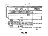
図15は、本発明の態様に従って側壁から弾性波を発生および受信する別の代替的なポリマー・フィルムから成るピエゾ・ストリップ350を示している。ピエゾ・ストリップ350では、ポリマー・ピエゾ・フィルム354の第1側部360に接地電極352が設けられている。第1電極356および第2電極358は、櫛歯状フィンガー360および370を有しており、ポリマー・ピエゾ・フィルム354の第2側部362に設けられている。ピエゾ・ストリップ350の第1部分364は、基板20の側壁32に取り付けられている。ピエゾ350の第2部分366は基板20を越えて延在し得、それゆえ、接地電極352、第1電極356および第2電極358に対して電気接続部を容易に取り付けることができる。側壁32に結合したピエゾ・ストリップ350は、図3の機構52に対して適用され得るオプションである。
FIG. 15 illustrates a
図16は、本発明の態様に従って形成されたタッチセンサー340のジオメトリーを示している。タッチセンサー340は、タッチ面24を有する基板20を有して成る。ピエゾ・ストリップ342〜348は、例えば接着剤を用いて、タッチ面24の外周部338に取り付けられている。例えば、ピエゾ・ストリップ342〜348は、図12に示すピエゾ・ストリップまたは図13に示すピエゾ・ストリップのいずれか一方であり得る。ストリップ342〜348は、矢印376の方向に示すような方向に弾性波を発生させたり、またはその方向の弾性波を受信したりする。ピエゾ・ストリップ342〜348は分かり易いように表しており、タッチセンサー340のサイズに応じて表していないことに留意されたい。
FIG. 16 illustrates the geometry of
図17は、本発明の態様に従って形成された図3の弾性波の発生または検出を行う機構52の側面図を示している。機構52は、第1電極84、圧電層83および外側電極86(例えば、図8に示すような櫛歯型の第1電極88および第2電極90、または図4に示すような第2電極)を有するように構成されている。機構52の第1電極84は、例えばエポキシなどから成る接着剤層85を用いることによって、側壁32に結合している。場合によっては、電極84,86に電気接続部を取り付けることができるように、機構52はタッチ面24を成す平面またはそれと対向する基板20の側部28のいずれか一方または双方を越えて延在してよい。
17 shows a side view of a
図18は、本発明の態様のU1方向(図6)における電極フィンガー82(図4)の相互の間隔または距離を示している。無次元水平偏波の剪断波(ZOHPS波または「GAW」として知られている)の送信および受信が所望の角度を成して行われるようになり、図6に示すような「U」弾性波経路および「V」弾性波経路が得られるように、図4で説明した電極フィンガー82の相互の間隔を調整することができる。基板20は、高さ116および幅118を有している。実線110および点線111は、水平側面113から生じた弾性波の最大および最少(最大の場合と同様の大きさを有する最も負となる振幅)をそれぞれ表している。水平軸方向に水平側面113に投影された最大箇所の間隔はSwとして表される。水平側面113から生じた弾性波は、矢印112で示すように垂直側面114に向かって進行する。垂直側面114に投影された最大箇所(および最少箇所)の間隔はSHとして表される。SwおよびSHの量は次の式で表される:
Sw=λ(H2+W2)1/2/W
SH=λ(H2+W2)1/2/H
波長λは、タッチ検知用にタッチセンサーで用いられる弾性波モードの位相速度Vおよび動作周波数fから決められる(関係式λ=V/f)。SwおよびSHを用いて電極フィンガー82の間隔を上述のように設定すると、矩形状タッチ面20の対角線に平行な弾性波にコヒーレント結合がもたらされ、タッチ・エリアにて二次元座標の測定を可能にするU1,U2,V1およびV2弾性波経路がもたらされる。
FIG. 18 illustrates the mutual spacing or distance of the electrode fingers 82 (FIG. 4) in the U1 direction (FIG. 6) of aspects of the present invention. Transmission and reception of dimensionless horizontally polarized shear waves (known as ZOHPS waves or “GAW”) are made at a desired angle, resulting in a “U” elastic wave as shown in FIG. The mutual spacing of the
S w = λ (H 2 + W 2 ) 1/2 / W
S H = λ (H 2 + W 2 ) 1/2 / H
The wavelength λ is determined from the phase velocity V and the operating frequency f of the elastic wave mode used in the touch sensor for touch detection (relational expression λ = V / f). When using S w and S H to set the interval of
図19は、本発明の態様に従って、圧電材料83などの電場に起因して膨張および収縮する圧電フィルム(例えばPVDFフィルムまたは焼成圧電セラミック層)と弾性波とが結合されるU1領域の結合機構を示している。黒矢印120は剪断弾性波の動きを表している。中抜き矢印124は、図8に示すような送信機構52(例えば、櫛歯電極88,90および圧電材料83)に起因する水平側面114沿った力を表している。同様の受信機構52が、垂直側面113に沿って設けられている。膨張する領域140は「+」記号で表され、収縮する領域142が「−」記号で表されている。
FIG. 19 shows a coupling mechanism in the U1 region where a piezoelectric film (eg, PVDF film or fired piezoelectric ceramic layer) that expands and contracts due to an electric field, such as the
圧電材料83が焼成圧電コーティングまたはポリマー層(PVDF層など)である場合、圧電挙動を呈するように、電場を用いて双極子モーメントを誘発して圧電材料83を分極処理(またはポーリング)する。図17を用いて説明する。市販の電極構造を用いると、側壁32に垂直な方向に圧電材料83を最も容易に分極処理できる。矢印144の方向に分極処理された圧電材料83においては、第1電極84および外側電極86に電圧が加えられると、加えられた電場に平行な方向144に膨張または収縮が生じると共に(本明細書では「33」結合と呼ぶ)、電場に垂直な方向であって側壁32に平行な方向146に膨張または収縮が生じることになる(本明細書では「31」結合と呼ぶ)。圧電材料83の特性に依存して、「31」結合に起因した146の方向の収縮または膨張は、基板20のタッチ面24に対して平行となるか又は垂直となり得る(または両方の場合もある)。このような圧電材料による3種類の結合の全て、即ち「33」結合および2種類の「31」結合は、所望の弾性波が発生する及び受信されるような結合を供すべく利用される。
When the
図19では、無次元の水平偏波の剪断波(ZOHPS)などの水平偏波の剪断波の間の結合が示されている。黒矢印120は剪断波の動きを表しており、中抜き矢印124は、ピエゾ材料83の「31」結合に起因する力を表している(尚、矢印146は、タッチ面24の面内に存在するものである)。図示していないが、圧電材料83における「33」結合を用い、側壁32に垂直な剪断波動きの成分(黒矢印120の方向に示すような方向の成分)を励起して弾性波を発生させることができる。対角線方向に伝搬するレイリー波は3つの全ての軸に沿うような側壁32における材料運動と関連するので、「33」結合および2種類の「31」結合を用いて、レイリー波およびラム波を励起させることができる。
In FIG. 19, the coupling between horizontally polarized shear waves such as dimensionless horizontally polarized shear waves (ZOHPS) is shown. The black arrow 120 represents the movement of the shear wave, and the
例えば、所望の弾性波モードを最も効率的に発生または受信するように結合を利用し、望ましくない寄生弾性モードへの結合を最小限に抑えたタッチセンサー50または100の設計が望ましい。更に、トランスデューサー(例えば機構52または上述の他の機構)の設計は、所望モードの深さプロファイルに一部依存している。例えば、剪断波は、基板20の深さの全てまたは大部分を通るように進行し得、一方、レイリー波は、基板20のタッチ面24付近にのみ結合し得る。
For example, a
図20には、本発明の態様に従って、基板20内の無次元水平偏波の剪断波(ZOHPSまたは市場では「GAW」とも呼ばれる)の弾性波密度が表されている。ZOHPSまたはGAWは、矢印152〜156に示すように、基板20全体にわたって一様な弾性波エネルギー密度を有している。かかる弾性波の励起および検出を行うために、送信または受信を行うアクティブ機構52(圧電材料83から成る層を有して成り得る)が、側壁32に沿って深さ158方向に一様に結合していることが好ましい。
FIG. 20 illustrates the elastic wave density of a dimensionless horizontally polarized shear wave (also called ZOHPS or “GAW” in the market) in the
図21は、本発明の態様に従って、より高い次元のプレート波の送信状態を示している。機構52は、それぞれ対向する反対の極性の第1圧電素子164および第2圧電素子166を有している。第1圧電素子164および第2圧電素子166は、基板20の上部(タッチ面24)および底部(第2面28)に隣接するように側壁32に形成されている。従って、より高次元の水平偏波の剪断波(または別のより高次元のプレート波)が、タッチ面24近傍にて矢印168,170に示すように送信されると共に、第2面28近傍にて矢印172,174に示すように送信されることになる。
FIG. 21 illustrates a higher dimensional plate wave transmission state in accordance with an aspect of the present invention. The
図22は、本発明の態様に従って、レイリー波が送信される状態を示している。レイリー波の弾性波密度は、矢印192,194で示すように、タッチ面24付近で高くなっている。方向146がタッチ面24に対して垂直となっている場合に「31」結合を行うには、レイリー波の約1波長λ176分の距離だけ基板20のタッチ面24から離れる領域までに、機構52の圧電材料83の活性エリアを制限することが望ましい。機構52の深さ158がレイリー波の1波長λ176に相当するように示しているものの、圧電材料83の活性エリアをタッチ面24からレイリー波の約1波長λ176以内のエリアに制限するのであれば、機構52の深さ158方向の長さはより大きくてもよいことを理解されよう。
FIG. 22 illustrates a state in which a Rayleigh wave is transmitted according to an aspect of the present invention. The elastic wave density of the Rayleigh wave is high near the
図23は、本発明の態様に従って、主として「33」結合を介してレイリー波と結合する機構52の圧電材料83を示している。矢印196,198に示すようなレイリー波の縦運動の位相は、極性が深さ158方向において反転している。それゆえ、機構52の活性圧電材料83の層が、異なる深さにて異なる極性で励起される。一般的に、シミュレーションと実験とを組み合わせることによって、所望の弾性波モードおよび分極した圧電層の圧電特性に応じて、機構52の活性圧電材料83の層の構造を決定することができる。
FIG. 23 illustrates a
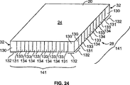
図24は、本発明の態様に従って、周期的な変調層(periodic modulation layer)134を有するトランスデューサー構造を示している。図2に示すような基板20を用いることができる。上述したように、基板20は、ガラス、セラミックおよび金属(アルミニウムまたはスチール)などのいずれの材料から形成してもよい。ある用途では、弾性波の損失が少ないガラスを使用することが望ましい。上述したように、基板の側壁32はクリーンな状態となっている。
FIG. 24 illustrates a transducer structure having a
基板20の側壁32の各々に第1導電層130を設けてもよく(または塗布によって第1導電層130を設けてもよく)、その場合、第1導電層130は、圧電トランスデューサー用の第1電極として機能し得る。導電層の材料としては、銀フリット、銅トレースまたはスクリーン印刷可能な導電性インクなどの適当な材料を用いることができる。例えば、第1導電層130は、スクリーン印刷用のインクを側壁32に塗布した後で高温下(例えば450℃)に付して焼成したものであってよい。
A first
その後、圧電材料層131が側壁32に適用されるが、圧電材料層131は第1導電層130上に適用される。圧電層131として用いることができる材料としては、制限するわけではないが、ポリマー圧電材料および焼成圧電セラミック材料を挙げることができる。場合によっては、第1導電層130への電気接続を可能とするために、コーナー付近に領域132を残しておいてもよい。
Thereafter, the
次いで、第2導電層133が設けられる。第2導電層133は、圧電トランスデューサー用の第2電極として機能し得る。典型的には、第1導電層130が、電磁的干渉に対する影響を最小限にするように、接地電極として機能し得、第2導電層133が、励起電極または受信信号電極として機能し得る。図4に示す電極80と違って、第2導電層133は圧電層131を被うように連続的に形成されており、それゆえ、櫛歯状フィンガーの電極構造を有していない。その代わりに、周期的な変調層134が、第2導電層133上に設けられている。
Next, a second
周期的な変調層134は、周期的な構造から成っており、基板20の上部(またはタッチ面24)から底部(または第2面28)まで実質的に延在しており、側壁32に沿って「ストリップ」として周期的に設けられた材料を含んで成る。それゆえ、側壁32には、第1導電層130、圧電層131、第2導電層133および周期的な変調層134が積み重なるように配置されており、それによって、トランスデューサー141(タッチセンサー50のタッチ領域40を横断する弾性波を発生または検出するためのトランスデューサー)が構築されている。
The
トランスデューサー141の周期的な変調層134は、トランスデューサー141によって送信または検出される弾性波を空間的に変調するように機能する。周期的な変調層134が存在すると、圧電層131の送信特性が変調されることになる。第1電極130と第2電極133との間で振動電圧が加えられると、圧電層131が機械的に励起される。圧電特性の「33」結合によって、側壁32に垂直な方向に圧電層131が膨張および収縮するので、側壁32の垂直面に対して力が生じる。圧電性の「33」結合の2つの方向によって、側壁32の面に対して平行な方向に膨張および収縮が生じるので、側壁32の垂直面に対して2方向の剪断力が加えられることになる。このような圧電結合の1つ以上は、所望の弾性波モードを発生および受信するのに有用である。例えば、弾性波にコヒーレント結合して、弾性波経路U1,U2,V1,V2を形成するには、図18で説明したように、弾性波の最大箇所と最小箇所との間隔を調整して、圧電トランスデューサーを調整しなければならない。周期的な変調層134を用いない場合では、側壁32に垂直な方向に弾性波がコヒーレント的に発生する。しかしながら、周期的な変調層134を用いて、対角線方向に伝搬する弾性波に対してコヒーレント結合する場合では、圧電特性の「33」結合を用いて、水平偏波の剪断波(例えばZOHPS)の励起および検出を行うことができる。水平偏波の剪断波が用いられたタッチセンサー50,100は、剪断波が水汚染に対して感度をほとんど有していないので、ある用途にとっては望ましいといえる。
The
周期的な変調層134によって、側壁32上の圧電トランスデューサーと基板20上の圧電トランスデューサーとの間の結合の振幅または位相が調整され得る。周期的な変調層134は、共振手段、位相シフト手段または吸収手段を有して成り得る。3つのケースが考えられる:
(1)圧電層131の厚さがλ/2よりも相当に小さく、周期的な変調層134が共振によって振幅を変調することを意図している場合に好ましいとされるケース(λは、基板20における圧力波ではなく、圧電層131における圧力波の波長);
(2)圧電層131の厚さがλ/2よりも幾分小さく、周期的な変調層134が共振周波数をシフトして位相を変調することを意図している場合に好ましいとされるケース;および
(3)圧電層131の厚さがほぼλ/2に等しく、周期的な変調層134が減衰効果によって振幅を変調することを意図している場合に好ましいとされるケース。
The
(1) The case where the thickness of the
(2) A case that is preferable when the thickness of the
図25および図26は、本発明の様態に従って、圧電機構206が1/2波長よりも相当に小さい厚さを有する圧電層を有して成る第1ケースの例を示している。圧電層131は、基板20上に一旦形成された後においては(焼成された後においては)、上述のポリマー−ピエゾ・ストリップよりも非常に硬いものである。図25に示す圧電機構206の部分には、周期的な変調層134が適用されておらず、圧電機構206がタッチセンサー50の動作周波数よりも相当に高い共振周波数(または共鳴周波数)を有することになる。圧電層131の膨張および収縮は、弾性波の発生または検出がされるように基板20へと効率的に結合していない。周期的な変調層134を備えた圧電機構206の部分は図26に示されている。周期的な変調層134を備えた圧電機構206が、タッチセンサー50(図3)の動作周波数(例えば5MHz)にて共振(または共鳴)するように、周期的な変調層134を選択して効率をより向上させることができる。弾性波減衰が少ない材料(例えばガラス・フリット)を用いて、圧電機構206を形成および調整してもよい。別法にて、厚さ200が1/2波長に設定されている場合、周期的な変調層134を用いて圧電機構206を離調(またはデチューン、detune)してもよい。
25 and 26 show an example of a first case in which the
図27は、本発明の態様に従って、圧電機構208が1/2波長よりも僅かに薄い厚さ200を有する圧電層131を有して成り、位相をシフトさせて変調を行う第2ケースの例を示している。図27に示す圧電機構208は変調層134を有しておらず、タッチセンサー50の動作周波数よりもわずかに高い共鳴周波数を有するように設計されている。図28に示す圧電機構208は変調層134を有しており、タッチセンサー50の動作周波数よりもわずかに低い共鳴周波数を有するように設計されている。
FIG. 27 shows an example of a second case in which the
図29は、本発明の態様に従って、ω0における共鳴を介して結合される位相および振幅の依存性を示している。実線150は、正規化された共振振幅A(グラフの左側の軸)を表している。点線151は、位相(°)(グラフの右側の軸)を表している。図29からは、共振する位相に対して位相を、ω0から例えば±45°または±60°シフトさせても、相当大きい振幅(最大振幅の約2/3程度の振幅)が存在しているので、共振振幅を依然多く残しつつ90°〜120°の範囲で位相変調を行うことができる。弾性波減衰の少ない材料を用いて、位相シフト変調層134を形成してもよい。
FIG. 29 shows the dependence of the phase and amplitude coupled via resonance at ω 0 in accordance with aspects of the present invention. A
第3ケース(図示せず)では、変調層134は吸収体として機能する。変調層134を備えていないトランスデューサー141が、基板へと強く結合するように動作周波数にて共振するように設計されている。吸収変調層134が設けられている箇所では、弾性波共振が大きく減衰する。吸収変調層の材料としては、金属(例えばタングステン)を含んだエポキシまたは他の超音波吸収材料を挙げることができる。
In the third case (not shown), the
図30は、本発明の態様に従って、レイリー波を発生させるように設計された圧電機構210を示している。機構52(図13および図14の機構52など)がレイリー波の深さプロファイルと適合するように深さが制限されていると、レイリー波用のエッジ・トランスデューサー(図4および図8の機構52など)は、より効率的となり、弾性波寄生信号をあまり生じない。それゆえ、図30において、圧電層131の活性領域の深さ212は、レイリー波の深さプロファイルと適合するように制限されている。このことは、圧電層131、第2電極133、変調層134、導電層130またはそれらの種々の組合せの深さ222に制限することによって、達成することができる。場合によっては、レイリー波を除く全ての弾性波モードを減衰させることが可能な層(図示せず)を基板20の底部(または第2面28)に設けることが望ましい場合がある。そのような減衰をもたらす層としては、基板20とデバイス(例えばディスプレイ)との間にてエポキシ層を有して成る硬質の光学結合部材が挙げられる。
FIG. 30 illustrates a
例えば付着させて周期的な変調層134を導電層133上に設けることができるが、他の手法によって周期的な変調を達成してもよい。例えば、周期的になるように選択領域をアニーリングにより不活性にすることによって、圧電層131自体を変調することができる。例えば、相転移点(例えばセラミック材料のキュリー点)よりも高く圧電材料を局所的に加熱することによって、圧電層131自体を変調してもよい。
For example, the
図31は、本発明の態様に従って、基板20を周期的に変化させて変調を得る例を示している。例えば、レーザー・ビーム等の局所的なエネルギー源を用いて基板20を周期的にマーキング処理135して、周期的構造を形成することができる。基板20がガラスである場合、3倍周波数のNd:YAG(355nm)を用いて、基板20の内部領域にて微細にガラス加工することができる。微細に加工されたガラスの弾性波特性は変化し得(例えば減衰または散乱が増加する)、そのようなガラスは、弾性波へのコヒーレント結合を周期的に変調させるのに用いることができる。換言すれば、基板20の内側にて複数のマーキング処理部135が規則正しい間隔を空けるように、光学的回折格子を形成することができる。一般的に、側壁32に設けたトランスデューサー141の弾性波挙度を調整する他の手段を用いると、周期的な変調層134を用いなくてもよい。例えば、圧電層131は、圧力モード・ピエゾであってよい。
FIG. 31 shows an example of obtaining modulation by periodically changing the
図24を参照して説明すると、連続的に設けられた層(第1導電層130、圧電層131、第2導電層133)を焼成してトランスデューサー141を形成してもよい。つまり、層130,131および133は、未硬化材料の形態で供した後に熱硬化に付す。変調層134も「焼成」してよい。焼結温度が比較的低い銀含有セラミックは、ガラス基板に導電トレース(conductive trace)を形成するのに用いられる材料として良く知られており、スクリーン印刷可能な形態で利用することができる。例えば、導電層130,133を形成するのに、銀フリットを用いることができる。図16Bおよび図17Bに示すような変調層134に対しては、弾性波損失の少ない硬い材料を用いてよく、その場合、製造の便宜上、導電層130,133に用いる材料と同じ材料を用いてよい。別法にて、変調層134を減衰層として機能させる場合では、変調層134を熱硬化性タングステンポリマーから形成してよい。
Referring to FIG. 24, the
焼成された層を有する図24に示される構造の態様では、層131に用いる圧電材料の適用な例として、Al2O3ゾル−ゲル溶液中に分散したPZT粒子およびPZTゾル−ゲル溶液中に分散したLiTaO3粒子などのゾル−ゲル状の圧電材料を挙げることができる。そのようなゾル−ゲル溶液を焼成処理することによって、50〜100μmの厚さのフィルムを得ることができる。他の圧電材料を用いてよく、例えば、Sr添加ニオブ酸カリウムナトリウム、または、ビスマス含有圧電セラミックなどの鉛フリー圧電セラミックを用いてもよい。スクリーン印刷またはスプレーコーティングなどの適当な方法によって、そのような圧電材料を塗布することができる。変調層134に用いられる上述のような材料は、未硬化状態で塗布した後、加熱により硬化に付され得る。層130,131,133および134の材料は、それぞれ連続的に塗布して硬化に付したり、または、全て塗布した後で同じ加熱サイクルで同時に硬化してもよく、あるいは、それらを組み合わせたような態様(ある層まで連続的に塗布して硬化させた後で残りの層については同じ加熱サイクルで同時に硬化させる態様)でもよい。
In the embodiment of the structure shown in FIG. 24 having a fired layer, as an example of application of the piezoelectric material used for the
圧電層131の圧電材料として焼成処理される材料を用いる場合、それを圧電体として機能させるために分極処理を施す必要がある。分極処理は、導電層130と導電層133との間に大きな電圧を加え、それによって、圧電層131の材料に大きい電場を発生させることによって行うことができる。このような分極処理は、圧電材料の強誘電キュリー点を越える温度で行われ得る処理工程の後で行わなければならない。
When a material to be fired is used as the piezoelectric material of the
電層131の圧電材料として焼成処理される材料を用いる場合、基板材料は、圧電材料の焼成温度および引き続くアニーリング温度(または焼なまし温度)に耐えることができるように選択しなければならない。例えば、コーニング1737を用いることができる。コーニング1737のアニーリング点は721℃であり、軟化点は957℃であり、いずれも、上述のゾル−ゲル組成物(Al2O3ゾル−ゲル溶液中に分散したPZT粒子およびPZTゾル−ゲル溶液中に分散したLiTaO3粒子)の焼成温度(450℃)およびアニーリング温度(650℃)よりも高くなっている。
When a material to be fired is used as the piezoelectric material of the
圧電トランスデューサー141を基板20とは別個に形成し、圧電トランスデューサー141をアッセンブリとして適用してもよい。例えば、かかるアッセンブリは、接着剤または他の適当な結合手段を用いて基板20に結合されたストリップ(上記で説明したようなストリップ)であってよい。接着剤層または結合層は、タッチセンサー50の弾性波作用に与える影響を最小限とするように薄いことが好ましく、満足のいく程度の範囲で弾性波減衰をもたらさないものが好ましい。第1導電層130、圧電層131、第2導電層133およびオプションとしての変調層134を有して成る層状アッセンブリは、例えば、厚さ100〜120μmのガラスのマイクロシート134を有して成るストリップ材料上に形成することができる。その場合、層状アッセンブリを更に分割(例えば、ダイシング)すると、複数の基板20に結合させることができる複数のトランスデューサー141を得ることができる。
The
図32は、本発明の態様に従って、基板20に形成された格子状トランスデューサー400を示している。第1トレース406が第2面28に形成されている。第1トレース406は、銀フリットなどの導電材料を含んで成る。第1トレース406は、スクリーン印刷法、パッド印刷法または他の付着法を用いて、塗布され得る。圧力モードの圧電素子408の第1側部410は、第1トレース406の一部上に設けられ、その第1トレース406の一部と相互に接続されている。第2トレース414は第2面28上に形成されている。第2トレース414は、圧電素子408の側面418および第2側部412に設けられており、それらと相互に接続されている。以下で更に説明するが、圧電素子408を励起させる電気接続部が、第1トレース406および第2トレース414の各々と相互に接続されている。
FIG. 32 illustrates a
格子要素402がタッチ面24に形成されている。格子要素402は、レイリー波の波長に相当する間隔404を空けて形成されている。格子要素402は、上述したようなスクリーン印刷またはエッチング等によって、材料を供したり又は除去したりすることによって形成さえ得る。また、反射アレイ416がタッチ面24に形成されている。反射アレイ416も、材料を供したり又は除去したりすることによって形成され得る。
A
図33は、本発明の態様に従って、基板20に形成された櫛状トランスデューサー420を示している。図32の場合と同様、格子要素432がタッチ面24に形成されている。第1トレース422は、格子要素432上に位置するようにタッチ面24に形成されている。厚さモードの圧電素子426の第1側部424は、第1トレース422の一部の上に適用され、その一部と相互に接続されている。第2トレース430がタッチ面24に形成されている。第2トレース430は、圧電素子426の側面434および第2側部428に適用され、それらと相互に接続されている。
FIG. 33 illustrates a
図34は、本発明の態様に従って、基板20に形成された櫛歯型トランスデューサー(interdigital transducer)440を示している。第1トレース442および第2トレース444が基板20のタッチ面24に形成されている。第1トレース442および第2トレース444は、図8の第1電極88および第2電極90等の櫛歯状フィンガー(図示せず)を有している。圧電素子448は、第1トレース442および第2トレース444の上に適用されており、それらと相互に接続されている。
FIG. 34 illustrates an
図35は、本発明の態様に従って、タッチ面24の外周部486に形成されたトランスデューサー452〜458を備えたタッチセンサー450を示している。反射要素460は、エッジ462〜468に対して45°の角度を成すように設けられており、外周部486内で反射アレイを形成している。
FIG. 35 shows a
トランスデューサー452〜458は、図32〜図34に示すトランスデューサー400,420または440のいずれか1つを成すものである。第1トレースおよび第2トレース470〜484は、エッジ466,468に隣接するようにタッチ面24に印刷されており、図示する適切なトランスデューサー452〜458と相互に接続されている。かかる相互接続は、用いられるトランスデューサーの種類によって決められる。第1トレースおよび第2トレース470〜484は、はんだ付け等によってケーブル488と相互に接続されている。
The transducers 452-458 constitute any one of the
図36は、本発明の態様に従って、基板20に形成された代替的なトランスデューサー490を示している。第1トレース492および第2トレース494はタッチ面24に適用されている。図36では1つのトレースしか示していない。第1トレース492および第2トレース494では、図34で説明したような櫛歯電極が形成されている。圧電素子498の第1側部550は、第1トレース492および第2トレース494上に適用されている。接地電極548は、タッチ面24、圧電素子498の第2側部552および側面554に適用されている。
FIG. 36 illustrates an
図37は、本発明の態様に従って、タッチ面24の外周部544に形成されたトランスデューサー502〜508を備えたタッチセンサー500を示している。反射アレイ510は、エッジ512〜518に対して45°を成すように設けられている。
FIG. 37 illustrates a
トランスデューサー502〜508は、図36のトランスデューサー490を成し得る。接地トレース、第1トレースおよび第2トレース520〜542は、タッチ面24に印刷されており、適切なトランスデューサー502〜508と相互に接続されている。接地トレース、第1トレースおよび第2トレース520〜542は、はんだ付け等によってケーブル546と相互に接続され得るものである。
The transducers 502-508 can form the
図35および図37を参照して説明する。コントローラー(図示せず)は、必要に応じて、第1電極および第2電極を介してトランスデューサーに電気信号を送るように機能し、また、接地電極を介してアース部に電気信号を送るように機能する。一回につき1つのトランスデューサーのみが活性化される。図示する態様では、4つのトランスデューサーが用いられている。そのうちの2つのトランスデューサーは送信トランスデューサーとして機能し得、別の2つのトランスデューサーは受信トランスデューサーとして機能し得る。送信または受信を行う2つまたは3つのトランスデューサーを有する他の形態または送信と受信との双方を行う2つまたは3つのトランスデューサーを有する他の形態を構築してタッチセンサーからの信号を受信してもよく、あるいは、タッチ面24の種々の部分またはエリアを被うような他の形態を構築してもよいことを理解されよう。
This will be described with reference to FIGS. 35 and 37. FIG. A controller (not shown) functions to send an electrical signal to the transducer via the first electrode and the second electrode, if necessary, and to send an electrical signal to the grounding part via the ground electrode. To work. Only one transducer is activated at a time. In the embodiment shown, four transducers are used. Two of them can function as transmitting transducers and the other two can function as receiving transducers. Build other forms with two or three transducers to transmit or receive or other forms with two or three transducers to both transmit and receive to receive signals from touch sensors It will be appreciated that other forms may be constructed, or alternatively, cover various portions or areas of the
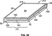
図38は、本発明の態様に従って形成された代替的なタッチセンサー214を示している。側壁32およびエッジ22は、上述したようなクリーンな状態となっている。基板20の側壁32には、トランスデューサー160、導波路161および反射アレイ162が配置されている。反射アレイ162は、エッジ22に隣接して形成され得るか、または、エッジ22を横断するように形成され得る。各々の側壁32に設けられているトランスデューサー160、導波路161および反射アレイ162は、機構171と呼ぶことができる。場合によっては、基板20のタッチ面24に、付加的な導波路および関連するアレイを形成してもよい。図38に示すように、弾性波の発生、方向付けおよび検出を行うタッチセンサー機構171に必要とされる導波路161および反射アレイ162を側壁32に配置することによって、ボーダー・エリア216を更に減じることができる。反射アレイ162および導波路161は、基板20に設けられた溝として形成してよく、または、基板20の側壁32に供された材料から成る突出部として形成してもよい。トランスデューサー160は、導波路161に結合される弾性波を発生させる。導波路161のコア部では弾性エネルギーが集束する。弾性波エネルギーは、アレイ162によって、表面弾性波として基板20に結合され得る。トランスデューサー160、導波路161およびアレイ162を有して成る機構171は、弾性波を発生させ、それをタッチセンサー214のタッチ領域24を横切るように方向付けるように機能し得、または、タッチセンサー214のタッチ領域24を横断した後の弾性波を検出するように機能し得る。
FIG. 38 illustrates an
弾性波が導波路161に沿って進行するつれ、そのエネルギーが損失していくことになる。多くのタッチセンサー214用途では、検出器(機構171など)によって受け取られる弾性波エネルギーが、通ってきた経路の長さに強く依存されないことが望ましい。それゆえ、経路長さに応じて信号振幅を均等化するように設計された種々の反射アレイ等、種々の弾性波信号等化方式を組み込んでもよい。信号振幅を均等化する設計には、反射アレイを構成する反射要素の高さの変更または幅の変更、または、反射要素の寸法の変更が挙げられる。
As the elastic wave travels along the
図39は、本発明の態様に従って信号の均等化を行うように配置された導波路161を示している。トランスデューサー160、導波路161および反射アレイ162は、タッチセンサー基板20の側壁32に配置されるものとして表している。導波路161は、側壁32の長さ218方向に湾曲して形成されている。導波路161は、その内部における弾性波エネルギーが最も高くなるトランスデューサー160付近の第1端部220においては、アレイ162から最も離れるように配置されている。その一方、トランスデューサー160から離れた第2端部222(導波路161は、その内部における弾性波エネルギーが最も小さくなる)においては、アレイ162により近づくように配置されている及び/又はアレイ162と交差するように配置されている及び/またはアレイ162の上部に配置されている。そのように導波路161が湾曲しているので、信号の均等化を行うことができる。
FIG. 39 illustrates a
図40は、本発明の態様に従って、信号の均等化を行うように形成された導波路161を示している。導波路161のコア部は、トランスデューサー160から離れるにつれ(または第1端部220から第2端部222へと向かう方向に)狭く形成されており、効果的にコアの影響を弱めている。コア部の幅が減じられるにつれ、弾性波は導波路161に制限されなくなって広がることになり、反射アレイ161と重なる弾性波が増えることになる。この場合、テーパー形状の導波路のコアにおける波速度の効果をより際立たせるために、反射アレイ162の要素163の相互の間隔を変更してよい。図39および図40に示すように形成および/または配置された導波路161によってもたらされる信号均等化は、導波路161がタッチ面24に配置された態様であっても等しく好ましく適用され得ることを理解されよう。
FIG. 40 illustrates a
図41は、本発明の態様に従って形成されたタッチセンサー224の別の態様を示している。クリーンな側壁32を有する基板20が設けられている(図2参照)。ストリップ180(その軸方向に弾性波を伝搬させることが可能なストリップ)が設けられている。かかるストリップ180は、図38〜40の導波路161と同様の機能を有する導波路である。ストリップ180において伝搬する弾性波は、伸縮波、たわみ板波(もしくは曲げ板)または、他の種類の弾性波であり得る。ストリップ180は、ガラス基板20の側壁32に配置されている。ストリップ180は、結合要素187を有して成る結合層186を介して、側壁32と結合している。ストリップ180の一方の端部181には、圧力モードの圧電素子183が設けられており、ストリップ180の対向する端部182には、エネルギー・ダンプ領域(energy dump region)184が必要に応じて設けられている。エネルギー・ダンプ領域184は、ストリップ180の一方の端部に設けられ得、それによって、反射が抑えられる。エネルギー・ダンプ領域184は、基板20の弾性波インピーダンスと適合するように調整することが可能な適当な材料(例えばタングステン含有エポキシ)を含んで成るものであってよい。ストリップ180で生じた弾性波は、基板面24で行われるタッチに対して感度を有するものであり、基板20にて弾性波に結合される。
FIG. 41 illustrates another embodiment of a
ストリップ180は、弾性波が伝搬できる材料(例えば金属またはガラス)を含んで成り得る。ストリップ材料の熱膨張係数(CTE)は、基板の熱膨張係数と近い値である。ある用途では、ストリップ180の高さ(側壁32の高さ方向に測定される高さ)がガラス基板厚さと略等しいことが有利となり得る。ストリップ180の厚さ(ストリップ高さに垂直な方向に測定される厚さ)は、基板20から大きく離れて延在しないように薄いことが好ましく、それによって、タッチセンサー224の外側エッジのサイズを最小限に維持することができる。ストリップ材料としては、ガラス・ロッドおよびガラスのCTEに近いCTEを有する金属ストリップ(例えば、Invar(登録商標)などのニッケル・アロイまたはそれに関連のある材料)を挙げることができる。ストリップ材料の断面形状の適当な例は、3mm×1mmの矩形状の断面および1/2mm×1/2mmの正方形状の断面である。
The
圧電素子183が電気的に励起されることによって、例えば、ストリップ180に沿って長手方向に伝搬する波が生じ得る。ストリップ180の断面に起因した境界条件に起因して、ストリップ180における波は、純粋な圧力波ではなく、伸縮波、対角線方向に向かう波、またはより次元の低い対称的なラム波といえる。長手方向成分を有する波が伝搬するので、ストリップ180の材料は、波の伝搬方向に対して平行に動く成分(即ち、ストリップ180の長さ方向に動く成分)を有している。
Electrical excitation of the
結合層186によって機械的な結合が供され、周期的に離隔した結合要素187の間隔によって、ストリップ180で生じた波が基板20へと形成される弾性波へと散乱する際の散乱角が決められる。結合要素187は、反射アレイと同様な周期的な構造を有するように形成される。例えばタッチセンサー224が矩形であって、側壁32に対して90°で散乱されることが望ましい場合、結合要素187の間隔をストリップ180の弾性波の波長に等しくしなければならない。90°の散乱は、図41にて矢印188で表されている。結合機構の1つの例として説明すると、結合要素187が剪断力を移動させるので、ストリップ180における波の長手方向の運動が、図41の矢印189に示されるように基板20における剪断波の横断方向の運動へと結合することになる。結合要素187の圧縮剛性によって、ストリップにおける波の横断方向運動が、基板20でのタッチ検知波運動(例えばレイリー波の運動)の長手方向成分と結合され得る(かかる結合態様は図示していない)。また、ストリップ180は、基板20からの弾性波を受信するようにも機能し得る。
The
図42は、本発明の態様に従ってストリップ180が組み込まれたタッチセンサー226を示している。ストリップ180は、分かりやすくするために、ストリップ228および230として表している。圧電素子232を有する第1ストリップ228は、基板20の第1側壁234に沿って配置されている。圧電素子236を有する第2ストリップ230は、基板20の第2側壁238に沿って配置されている。矢印190で示されるように、圧電素子232で生じた後、ストリップ228によって基板20に向かうように方向付けられた剪断波は、側壁240で反射し得、その後、ストリップ228で方向を変えられ、圧電素子232によって検出されることになる。矢印191で示すように、圧電素子236で生じた後、ストリップ230によって基板20に向かうように方向付けられた剪断波は、側壁242で反射し得、その後、ストリップ230で方向を変えられ、圧電素子236によって検出されることになる。圧電素子232および236に接続されている電子機器(図示せず)は、信号を時分割多重して、送信モードと受信モードとの間を調整するのに用いられ得る。
FIG. 42 illustrates a
別法にて、タッチセンサーは、全ての側壁32にストリップが設けられているものでもよい(図示せず)。例えば矩形の基板20に対しては、4つのストリップ180が用いられる。その場合、そのうちの2つのストリップ180を送信モードで機能させ、また、別の2つのストリップ180を受信モードで機能させてもよい。
Alternatively, the touch sensor may be provided with strips on all side walls 32 (not shown). For example, for the
基板20の側壁32に設けられているストリップ180が基板20にてレイリー波を励起するように設計されている場合では、図22および図23に示すレイリー波へと効率的に結合するように、結合要素187が、タッチ面20からレイリー波の約1波長分だけ離れた領域内にて側壁32に結合している必要がある。ストリップ180の深さ寸法は、結合要素187の深さ寸法と適合していてよいし、適合してなくてもよい。
In the case where the
ストリップ180と基板20との結合強さは、結合要素の堅さ、厚さまたは結合エリアのいずれか1つ以上によって影響を受けるものである。好ましくは、基板20へと結合する弾性波の振幅は、結合が行われる側壁32上のポイントからは独立している。ストリップ180と基板20との結合に影響を与えるパラメーターを用いることによって、基板20に沿った距離に応じて(または基板20に沿った距離の関数として)弾性波信号の振幅を均等化させることができる。
The bond strength between the
図41は、結合材料が存在している箇所(結合要素187)と結合材料が存在していない箇所とが交互に設けられた結合層186のケースを示している。このような結合層186では、ストリップ180と基板20との結合強さが空間的に調整されている。別の手段によっても、結合を空間的に所望に調整できる。例えば、結合材料の機械的性質が調整されるように、空気ギャップが存在しない結合層が考えられる。ストリップ181および結合要素187を基板20とは別個に形成した後、それらをアッセンブリとして取り付けてもよいことを理解されよう。
FIG. 41 shows a case of the
図43は、本発明の態様に従って基板20の側壁32に形成されたトランスデューサー562を備えたタッチセンサー560を示している。励起されると、トランスデューサー562は、エッジ22に沿って進行するエッジ波を発生させる。かかるエッジ波は、反射アレイ564によって、タッチ面24を横切るように反射することになる。このようなタッチセンサーは、米国仮特許出願第60/562461号(代理人整理番号ELG064−US1)に開示されており、かかる仮出願の内容は、引用することにより本明細書に組み込まれる。トランスデューサー562は、スクリーン印刷または他の上述した手法で側壁32に印刷された圧電材料を含んでいるものでもよい。別法にて、トランスデューサー562は、個々に形成された後で側壁32に結合された圧電材料を含んでいるものであってよい。
FIG. 43 illustrates a
本明細書で説明したタッチセンサーのいずれの態様の場合であっても、タッチセンサーを、電気的相互接続手段によって、コントローラーと接続させることができる。例えば、ケーブルハーネスなどの適当な相互接続手段を用いることができる。別法にて、タッチセンサーをタッチセンサー・システムに直接的に組み込んでもよい。例えば、タッチセンサーとディスプレイとを一体化してタッチスクリーンを形成してもよい。場合によっては、真空蛍光ディスプレイに使用される基板の面(例えばインストルメント・パネル)に対してスクリーン印刷を行ってもよい。例えば、基板が、真空蛍光ディスプレイ等のディスプレイ・デバイスの外側層を成すものであってもよい。 In any aspect of the touch sensor described herein, the touch sensor can be connected to the controller by electrical interconnection means. For example, suitable interconnection means such as a cable harness can be used. Alternatively, the touch sensor may be incorporated directly into the touch sensor system. For example, a touch screen may be formed by integrating a touch sensor and a display. In some cases, screen printing may be performed on a surface of a substrate (for example, an instrument panel) used in a vacuum fluorescent display. For example, the substrate may form the outer layer of a display device such as a vacuum fluorescent display.
上記で説明した装置の構成は単に例示的に本発明の原理の応用例を説明したにすぎず、本発明の概念および範囲を逸脱しないことを前提として他の態様および変更も可能であることを理解されよう。尚、上述のような本発明は、次の態様を包含している:
第1の態様:弾性波を伝搬させることが可能な基板であって、タッチ検知領域を有する第1面および該第1面と第1エッジにて交差している第1側壁を含んだ基板、ならびに
基板の第1側壁に設けられたトランスミッターであって、タッチ検知領域の少なくとも一部を通るように第1側壁から直接的に伝搬する弾性波を発生させるトランスミッター
を有して成るタッチセンサー。
第2の態様:上記第1の態様において、第1面と第1側壁とは第1エッジにて約90°の角度を成すように交差しているタッチセンサー。
第3の態様:上記第1の態様において、トランスミッターが弾性波の向きを第1側壁に対して垂直な方向に変えるタッチセンサー。
第4の態様:上記第1の態様において、トランスミッターが、第1側壁に沿って周期的に連続するように形成された構造の第1電極を更に有して成るタッチセンサー。
第5の態様:上記第1の態様において、トランスミッターが第1電極および第2電極を更に有して成り、第1電極および第2電極の各々が、第1側壁に沿って相互に交互に配置された連続的なフィンガーを含んでいる、タッチセンサー。
第6の態様:上記第1の態様において、側壁が第1端部および第2端部を有して成り、トランスミッターが第1端部に配置されており、
側壁が、それに沿うように方向付けられた導波路および第1面に隣接するように側壁に沿って配置された反射アレイを更に有して成る、タッチセンサー。
第7の態様:上記第1の態様において、トランスミッターは、側壁の高さ方向に向きを揃えたフィンガーを有する電極を含んでおり、フィンガーは、タッチ検知領域を横切るように向けられる弾性波の角度を調整するように相互に間隔を空けて配置されている、タッチセンサー。
第8の態様:上記第1の態様において、トランスミッターが、タッチ検知領域の少なくとも一部を伝搬する弾性波として、剪断波、ラム波またはレイリー波のいずれか1つを発生させるタッチセンサー。
第9の態様:上記第1の態様において、タッチ検知領域を横切って伝搬する弾性波が、第1側壁に対して鋭角を成す方向に伝搬するタッチセンサー。
第10の態様:上記第1の態様において、基板の第2側壁に設けられた検出器を更に有して成り、検出器がタッチ検知領域の少なくとも一部を横断した後の弾性波を検出する、タッチセンサー。
第11の態様:上記第1の態様において、トランスミッターが周期的な構造の第1トランスデューサーおよび第2トランスデューサーを更に有して成り、
第1トランスデューサーおよび第2トランスデューサーが、基板の対向する第1側壁および第2側壁にそれぞれ設けられ、第1トランスデューサーおよび第2トランスデューサーが、対向する第1側壁および第2側壁に対して鋭角を成す方向に伝搬する第1弾性波および第2弾性波を発生させる、タッチセンサー。
第12の態様:上記第1の態様において、トランスミッターが、弾性波を変調させる変調層を更に有して成り、それによって、弾性波の減衰、共振周波数に対する弾性波の同調および離調、または、弾性波の位相のシフトのいずれか1つが行われる、タッチセンサー。
第13の態様:弾性波を伝搬させることが可能な基板であって、タッチ検知領域を有する第1面および該第1面と交差している第1側壁および第2側壁を含んだ基板、
基板の第1側壁に設けられたトランスミッターであって、タッチ検知領域の少なくとも一部を横切るように第1側壁から直接的に伝搬する弾性波を発生させるトランスミッター、ならびに
基板の第2側壁に設けられた検出器であって、タッチ検知領域の少なくとも一部を横断した後の弾性波を検知する検出器
を有して成るタッチセンサー・システム。
第14の態様:上記第13の態様において、トランスミッターが第1電極および第2電極を更に有して成り、第1電極および第2電極の各々が第1側壁に沿って周期的な構造を有する、タッチセンサー・システム。
第15の態様:上記第13の態様において、トランスミッターは、基板の対向する第1側壁および第3側壁にそれぞれ設けられた第1櫛歯型トランスデューサーおよび第2櫛歯型トランスデューサーを更に有して成り、第1櫛歯型トランスデューサーおよび第2櫛歯型トランスデューサーが、対向する第1側壁および第3側壁に対して鋭角を成す方向に伝搬する第1弾性波および第2弾性波を発生させる、タッチセンサー・システム。
第16の態様:上記第13の態様において、側壁が第1端部および第2端部を有して成り、トランスミッターが第1端部に配置され、また、側壁が、それに沿うように方向付けられた導波路および第1面に隣接するように側壁に沿って配置された反射アレイを更に有して成り、
導波路が側壁に結合されたストリップまたは側壁から材料を取り除いて形成した溝のいずれか一方である、タッチセンサー・システム。
第17の態様:弾性波が伝搬することが可能な基板のタッチ検知領域にてタッチを検出する方法であって、基板にはタッチ検知領域を有する第1面が含まれ、基板が、第1面と交差している第1側壁および第2側壁を有しており、
基板の第1側壁の近傍で弾性波を発生させる工程、
基板の第1側壁の一部を通ってから基板へと進行し、その後、タッチ検知領域の少なくとも一部を横切るように弾性波を方向付ける工程、および
基板の第2側壁の近傍で弾性波を検出する工程
を含んで成る方法。
第18の態様:上記第17の態様において、タッチされた位置が示唆される弾性波における摂動を検出することが検出工程に更に含まれる方法。
第19の態様:上記第17の態様において、弾性波がタッチ検知領域の少なくとも一部を通過するように、第1側壁に沿って配置された波源から延びる直線方向へと弾性波を方向付け、弾性波が反射することなく単一の経路のみ進行することが検出工程に更に含まれる、方法。
第20の態様:上記第17の態様において、第1側壁に沿うように弾性波の向きを変え、弾性波を反射させることが、弾性波を方向付ける工程に更に含まれる、方法。
第21の態様:弾性波を伝搬させることが可能であって、タッチ検知領域を有する第1面を含んだ基板、および
基板に形成されたトランスデューサー
を有して成るタッチセンサーであって、
トランスデューサーが、基板に設けた後で熱硬化に付した圧電素子を有して成り、また、トランスデューサーが、弾性波の発生または弾性波の検出の少なくとも一方を行うように構成されている、タッチセンサー。
第22の態様:上記第21の態様において、圧電素子がスクリーン印刷またはパッド印刷のいずれか一方を用いて基板に形成されている、タッチセンサー。
第23の態様:上記第21の態様において、基板が第1面に平行な第2面を更に有して成り、トランスデューサーが、第1面に形成された格子要素を更に有して成り、格子要素に対向するように圧電素子が第2面に形成されている、タッチセンサー。
第24の態様:上記第21の態様において、トランスデューサーが、第1面に形成された格子要素を更に有して成り、格子要素上に圧電素子が形成されている、タッチセンサー。
第25の態様:上記第21の態様において、トランスデューサーが、
基板に形成された第1導電層、
第1導電層上に形成された、圧電素子を含んで成る第2導電層、
第2導電層上に形成された第3導電層
を更に有して成り、
第1導電層と第3導電層とが、第1電気接続部および第2電気接続部を用いて相互に接続されている、タッチセンサー。
第26の態様:上記第21の態様において、トランスデューサーが
基板に形成された第1層、
第1層上に形成された第2層、および
第2層上に形成された第3導電層
を更に有して成り、
第1層とアース接続部とが相互に接続されており、第2層が圧電素子を含んで成り、また、第3導電層が第1電極および第2電極を含んで成り、第1電極および第2電極と第1電気接続部および第2電気接続部とが相互に接続されている、タッチセンサー。
第27の態様:上記第21の態様において、基板が、ディスプレイ・デバイスの外側層を成している、タッチセンサー。
第28の態様:上記第21の態様において、トランスデューサーが、
基板に形成された第1導電層、
第1導電層上に形成された、圧電素子を含んで成る第2導電層、
第2導電層上に形成された第3導電層、および
第3導電層上に形成された、周期的に適用された材料を含んで成る第4変調層
を更に有して成り、
第1導電層および第3導電層が電気接続部と相互に接続されている、タッチセンサー。
第29の態様:弾性波を伝搬させることが可能であって、タッチ検知領域を有する第1面を含んだ基板、および
弾性波の発生または受信の少なくとも一方を行うように構成されているトランスデューサー
を有して成るタッチセンサーであって、
トランスデューサーが、圧電材料を有して成るストリップを含み、ストリップが基板に取り付けられている、タッチセンサー。
第30の態様:上記第29の態様において、圧電材料は、ポリマーのピエゾ材料を含んで成る、タッチセンサー。
第31の態様:上記第29の態様において、ストリップが、導電材料から成る層を少なくとも2つ更に有して成り、圧電材料が、その導電材料から成る2つの層の間に形成されている、タッチセンサー。
第32の態様:上記第29の態様において、第1面は、外周部を有するタッチ・エリアを更に有して成り、基板が、第1面に平行な第2面を更に有して成り、タッチセンサーが第1面の外周部内に形成された格子状トランスデューサーを更に有して成り、ストリップが格子状トランスデューサーと対向するように第2面に取り付けられている、タッチセンサー。
第33の態様:タッチ検知領域を有する第1面を含んだタッチセンサー基板にトランスデューサーを形成する方法であって、
基板に第1導電層を供する工程、
第1導電層の少なくとも一部が被われるように、基板に圧電層を供する工程、および
圧電層を熱硬化させる工程
を含んで成る方法。
第34の態様:上記第33の態様において、第2導電層によって圧電層の少なくとも一部が被われるように、基板に第2導電層を供する工程を更に含んで成る、方法。
第35の態様:上記第33の態様において、基板に第2導電層を供する工程、ならびに
第1導電層および第2導電層にそれぞれ第1電圧および第2電圧を加えて、圧電層を分極処理する工程
を更に含んで成る、方法。
第36の態様:上記第33の態様において、圧電層を供する工程には、圧電材料のスクリーン印刷が更に含まれる、方法。
第37の態様:上記第33の態様において、基板から材料を取り除くことによって基板に格子要素を形成することを更に含んで成り、第1導電層を供する工程および圧電層を供する工程には、第1導電層および圧電層を格子要素上に供することが更に含まれる、方法。
第38の態様:上記第33の態様において、
基板に導電トレースを形成する工程、および
電気信号が導電層に送られることになるように、導電性トレースと導電層とを相互に接続する工程
を更に含んで成る、方法。
第39の態様:上記第33の態様において、圧電材料がゾル−ゲル材料を含んで成る方法。
第40の態様:上記第33の態様において、基板が、第1面に対して実質的に垂直となるように第1面とエッジにて交差している側壁を更に有して成る方法。
The configuration of the apparatus described above is merely illustrative of an application example of the principle of the present invention, and that other modes and modifications are possible without departing from the concept and scope of the present invention. It will be understood. The present invention as described above includes the following aspects:
1st aspect: The board | substrate which can propagate an elastic wave, Comprising: The board | substrate including the 1st side which has a touch detection area | region, and the 1st side wall which cross | intersects this 1st surface at the 1st edge, And
A transmitter provided on a first side wall of a substrate, wherein the transmitter generates an elastic wave that propagates directly from the first side wall so as to pass through at least a part of the touch detection region.
Comprising a touch sensor.
Second aspect: The touch sensor according to the first aspect, wherein the first surface and the first side wall intersect each other at an angle of about 90 ° at the first edge.
Third aspect: The touch sensor according to the first aspect, wherein the transmitter changes the direction of the elastic wave in a direction perpendicular to the first side wall.
Fourth aspect: The touch sensor according to the first aspect, wherein the transmitter further includes a first electrode having a structure formed so as to be periodically continuous along the first side wall.
Fifth aspect: In the first aspect, the transmitter further includes a first electrode and a second electrode, and the first electrode and the second electrode are alternately arranged along the first side wall. Touch sensor, including a continuous finger.
Sixth aspect: In the first aspect, the side wall has a first end and a second end, and the transmitter is disposed at the first end.
A touch sensor, wherein the side wall further comprises a waveguide oriented along the side and a reflective array disposed along the side wall adjacent to the first surface.
Seventh aspect: In the first aspect, the transmitter includes an electrode having fingers oriented in the height direction of the side wall, and the fingers are angled of elastic waves directed across the touch sensing area. Touch sensors that are spaced apart from each other to adjust.
Eighth aspect: The touch sensor according to the first aspect, in which the transmitter generates any one of a shear wave, a Lamb wave, and a Rayleigh wave as an elastic wave propagating through at least a part of the touch detection region.
Ninth aspect: The touch sensor according to the first aspect, wherein the elastic wave propagating across the touch detection region propagates in a direction that forms an acute angle with the first side wall.
Tenth aspect: In the first aspect, the detector further includes a detector provided on the second side wall of the substrate, and the detector detects an elastic wave after crossing at least a part of the touch detection area. ,Touch sensor.
Eleventh aspect: In the first aspect, the transmitter further includes a first transducer and a second transducer having a periodic structure;
A first transducer and a second transducer are provided on opposite first and second side walls of the substrate, respectively, and the first and second transducers are opposed to the opposite first and second side walls. A touch sensor that generates a first elastic wave and a second elastic wave that propagate in a direction that forms an acute angle.
Twelfth aspect: In the first aspect, the transmitter further includes a modulation layer that modulates the elastic wave, thereby damping the elastic wave, tuning and detuning of the elastic wave with respect to the resonance frequency, or A touch sensor in which any one of the phase shifts of elastic waves is performed.
Thirteenth aspect: A substrate capable of propagating an elastic wave, the substrate including a first surface having a touch detection region, and first and second sidewalls intersecting the first surface;
A transmitter provided on a first side wall of the substrate for generating an elastic wave that propagates directly from the first side wall across at least a portion of the touch sensing region; and
A detector provided on the second side wall of the substrate for detecting an elastic wave after traversing at least a part of the touch detection area
A touch sensor system comprising:
Fourteenth aspect: In the thirteenth aspect, the transmitter further includes a first electrode and a second electrode, and each of the first electrode and the second electrode has a periodic structure along the first side wall. Touch sensor system.
Fifteenth aspect: In the thirteenth aspect, the transmitter further includes a first comb-shaped transducer and a second comb-shaped transducer respectively provided on the first and third side walls facing each other. The first comb-shaped transducer and the second comb-shaped transducer generate the first elastic wave and the second elastic wave that propagate in a direction that forms an acute angle with respect to the opposing first and third side walls. Let the touch sensor system.
Sixteenth aspect: In the thirteenth aspect, the side wall has a first end and a second end, the transmitter is disposed at the first end, and the side wall is oriented along the same. And further comprising a reflective array disposed along the side wall adjacent to the waveguide and the first surface,
A touch sensor system in which the waveguide is either a strip coupled to the sidewall or a groove formed by removing material from the sidewall.
Seventeenth aspect: A method for detecting a touch in a touch detection region of a substrate capable of propagating elastic waves, the substrate including a first surface having a touch detection region, wherein the substrate is a first Having a first side wall and a second side wall intersecting the surface;
Generating an elastic wave in the vicinity of the first side wall of the substrate;
Passing through a portion of the first side wall of the substrate and then to the substrate and then directing the elastic wave across at least a portion of the touch sensing area; and
A step of detecting an elastic wave in the vicinity of the second side wall of the substrate
Comprising a method.
Eighteenth aspect: The method according to the seventeenth aspect, wherein the detection step further includes detecting a perturbation in the elastic wave that indicates the touched position.
Nineteenth aspect: In the seventeenth aspect, the elastic wave is directed in a linear direction extending from a wave source disposed along the first side wall so that the elastic wave passes through at least a part of the touch detection region. A method wherein the detecting step further includes traveling only a single path without reflection of the elastic wave.
Twentieth aspect: The method according to the seventeenth aspect, wherein the step of redirecting the elastic wave includes changing the direction of the elastic wave along the first side wall and reflecting the elastic wave.
Twenty-first aspect: a substrate that is capable of propagating elastic waves and includes a first surface having a touch detection region, and
Transducer formed on the substrate
A touch sensor comprising:
The transducer includes a piezoelectric element that is subjected to thermosetting after being provided on the substrate, and the transducer is configured to perform at least one of generation of elastic waves or detection of elastic waves; Touch sensor.
Twenty-second aspect: The touch sensor according to the twenty-first aspect, wherein the piezoelectric element is formed on the substrate by using either screen printing or pad printing.
Twenty-third aspect: In the twenty-first aspect, the substrate further includes a second surface parallel to the first surface, and the transducer further includes a lattice element formed on the first surface, A touch sensor, wherein a piezoelectric element is formed on the second surface so as to face the lattice element.
Twenty-fourth aspect: The touch sensor according to the twenty-first aspect, wherein the transducer further includes a lattice element formed on the first surface, and a piezoelectric element is formed on the lattice element.
Twenty-fifth aspect: In the twenty-first aspect, the transducer comprises:
A first conductive layer formed on the substrate;
A second conductive layer formed on the first conductive layer and comprising a piezoelectric element;
Third conductive layer formed on the second conductive layer
And further comprising
A touch sensor in which a first conductive layer and a third conductive layer are connected to each other using a first electrical connection portion and a second electrical connection portion.
Twenty-sixth aspect: in the twenty-first aspect, the transducer is
A first layer formed on the substrate;
A second layer formed on the first layer; and
Third conductive layer formed on the second layer
And further comprising
The first layer and the ground connection portion are connected to each other, the second layer includes a piezoelectric element, and the third conductive layer includes a first electrode and a second electrode, The touch sensor in which the second electrode, the first electrical connection portion, and the second electrical connection portion are connected to each other.
Twenty-seventh aspect: The touch sensor according to the twenty-first aspect, wherein the substrate forms an outer layer of the display device.
Twenty-eighth aspect: In the twenty-first aspect, the transducer comprises:
A first conductive layer formed on the substrate;
A second conductive layer formed on the first conductive layer and comprising a piezoelectric element;
A third conductive layer formed on the second conductive layer; and
A fourth modulation layer comprising a periodically applied material formed on the third conductive layer
And further comprising
A touch sensor, wherein the first conductive layer and the third conductive layer are interconnected with the electrical connection portion.
Twenty-ninth aspect: a substrate that is capable of propagating elastic waves and includes a first surface having a touch detection region, and
A transducer configured to generate and / or receive elastic waves
A touch sensor comprising:
A touch sensor, wherein the transducer includes a strip comprising a piezoelectric material, and the strip is attached to the substrate.
30th aspect: The touch sensor according to the 29th aspect, wherein the piezoelectric material comprises a polymer piezo material.
Thirty-first aspect: In the twenty-ninth aspect, the strip further includes at least two layers made of a conductive material, and the piezoelectric material is formed between the two layers made of the conductive material. Touch sensor.
Thirty-second aspect: In the twenty-ninth aspect, the first surface further includes a touch area having an outer peripheral portion, and the substrate further includes a second surface parallel to the first surface, The touch sensor, further comprising a lattice-shaped transducer formed in the outer peripheral portion of the first surface, wherein the strip is attached to the second surface so as to face the lattice-shaped transducer.
Thirty-third aspect: A method of forming a transducer on a touch sensor substrate including a first surface having a touch detection area,
Providing a first conductive layer on the substrate;
Providing a piezoelectric layer on the substrate such that at least a portion of the first conductive layer is covered; and
Process for thermosetting the piezoelectric layer
Comprising a method.
Thirty-fourth aspect: The method according to the thirty-third aspect, further comprising the step of providing a second conductive layer on the substrate so that at least a part of the piezoelectric layer is covered with the second conductive layer.
Thirty-fifth aspect: in the thirty-third aspect, the step of providing a second conductive layer on the substrate; and
Applying a first voltage and a second voltage to the first conductive layer and the second conductive layer, respectively, to polarize the piezoelectric layer
A method further comprising:
Thirty-sixth aspect: The method according to the thirty-third aspect, wherein the step of providing a piezoelectric layer further includes screen printing of a piezoelectric material.
Thirty-seventh aspect: In the thirty-third aspect, the method further includes forming a lattice element on the substrate by removing material from the substrate, wherein the step of providing the first conductive layer and the step of providing the piezoelectric layer include: A method further comprising providing a conductive layer and a piezoelectric layer on the lattice element.
Thirty-eighth aspect: in the thirty-third aspect,
Forming conductive traces on the substrate; and
Interconnecting conductive traces and conductive layers such that an electrical signal will be sent to the conductive layers
A method further comprising:
Thirty-ninth aspect: The method according to the thirty-third aspect, wherein the piezoelectric material comprises a sol-gel material.
40th aspect: The method according to the 33rd aspect, wherein the substrate further comprises a side wall intersecting the first surface at the edge so as to be substantially perpendicular to the first surface.
関連出願の相互参照
本出願は、米国仮特許出願第60/562,461号(発明の名称:「弾性波タッチセンサー」、出願日:2004年4月14日)および米国仮特許出願第60/562,455(発明の名称:「弾性波タッチセンサー」、出願日:2004年4月14日)と関連があるものであり、その開示内容は引用することにより本明細書に組み込まれる。
CROSS-REFERENCE TO RELATED APPLICATIONS This application claims the benefit of US Provisional Application No. 60 / 562,461 No. (entitled "acoustic touch sensor", filed on Apr. 14, 2004) and U.S. Provisional Patent Application No. 60 / 562,455 (Title of Invention: “Acoustic Wave Touch Sensor”, filing date: April 14, 2004), the disclosure of which is incorporated herein by reference.
Claims (8)
基板に形成されたトランスデューサー
を有して成るタッチセンサーであって、
トランスデューサーが、基板に設けた後で熱硬化に付した圧電セラミック素子を有して成り、また、トランスデューサーが、弾性波の発生または弾性波の検出の少なくとも一方を行うように構成されている、タッチセンサー。A touch sensor capable of propagating an acoustic wave, comprising a substrate including a first surface having a touch detection region, and a transducer formed on the substrate,
The transducer includes a piezoelectric ceramic element that is heat-cured after being provided on the substrate, and the transducer is configured to perform at least one of generation of elastic waves or detection of elastic waves. ,Touch sensor.
基板に形成された第1導電層、
第1導電層上に形成された、圧電セラミック素子を含んで成る第2導電層、
第2導電層上に形成された第3導電層
を更に有して成り、
第1導電層と第3導電層とが、第1電気接続部および第2電気接続部を用いて相互に接続されている、請求項1に記載のタッチセンサー。The transducer
A first conductive layer formed on the substrate;
A second conductive layer comprising a piezoelectric ceramic element formed on the first conductive layer;
And further comprising a third conductive layer formed on the second conductive layer,
The touch sensor according to claim 1, wherein the first conductive layer and the third conductive layer are connected to each other using the first electrical connection portion and the second electrical connection portion.
基板に形成された第1層、
第1層上に形成された第2層、および
第2層上に形成された第3導電層
を更に有して成り、
第1層とアース接続部とが相互に接続されており、第2層が圧電セラミック素子を含んで成り、また、第3導電層が第1電極および第2電極を含んで成り、第1電極および第2電極と第1電気接続部および第2電気接続部とが相互に接続されている、請求項1に記載のタッチセンサー。A first layer in which a transducer is formed on a substrate;
A second conductive layer formed on the first layer; and a third conductive layer formed on the second layer;
The first layer and the ground connection portion are connected to each other, the second layer includes a piezoelectric ceramic element, and the third conductive layer includes a first electrode and a second electrode. The touch sensor according to claim 1, wherein the second electrode, the first electrical connection portion, and the second electrical connection portion are connected to each other.
基板に形成された第1導電層、
第1導電層上に形成された、圧電セラミック素子を含んで成る第2導電層、
第2導電層上に形成された第3導電層、および
第3導電層上に形成された、周期的に適用された材料を含んで成る第4変調層
を更に有して成り、
第1導電層および第3導電層が電気接続部と相互に接続されており、また
前記第4変調層の前記周期的に適用された前記材料が、共振材、移相材または吸収材を含んで成る、請求項1に記載のタッチセンサー。The transducer
A first conductive layer formed on the substrate;
A second conductive layer comprising a piezoelectric ceramic element formed on the first conductive layer;
A third conductive layer formed on the second conductive layer; and a fourth modulation layer formed on the third conductive layer and comprising a periodically applied material.
The first conductive layer and the third conductive layer are interconnected with electrical connections, also
The touch sensor according to claim 1, wherein the periodically applied material of the fourth modulation layer comprises a resonance material, a phase shift material, or an absorption material .
Applications Claiming Priority (3)
| Application Number | Priority Date | Filing Date | Title |
|---|---|---|---|
| US56245504P | 2004-04-14 | 2004-04-14 | |
| US60/562,455 | 2004-04-14 | ||
| PCT/US2005/012891 WO2005103872A2 (en) | 2004-04-14 | 2005-04-13 | Acoustic touch sensor |
Related Child Applications (2)
| Application Number | Title | Priority Date | Filing Date |
|---|---|---|---|
| JP2010080377A Division JP2010232664A (en) | 2004-04-14 | 2010-03-31 | Elastic wave touch screen |
| JP2010292087A Division JP2011123904A (en) | 2004-04-14 | 2010-12-28 | Elastic wave touch screen |
Publications (3)
| Publication Number | Publication Date |
|---|---|
| JP2007533039A JP2007533039A (en) | 2007-11-15 |
| JP2007533039A5 JP2007533039A5 (en) | 2010-05-20 |
| JP4989461B2 true JP4989461B2 (en) | 2012-08-01 |
Family
ID=34966016
Family Applications (3)
| Application Number | Title | Priority Date | Filing Date |
|---|---|---|---|
| JP2007508575A Expired - Fee Related JP4989461B2 (en) | 2004-04-14 | 2005-04-13 | Elastic wave touch screen |
| JP2010080377A Pending JP2010232664A (en) | 2004-04-14 | 2010-03-31 | Elastic wave touch screen |
| JP2010292087A Pending JP2011123904A (en) | 2004-04-14 | 2010-12-28 | Elastic wave touch screen |
Family Applications After (2)
| Application Number | Title | Priority Date | Filing Date |
|---|---|---|---|
| JP2010080377A Pending JP2010232664A (en) | 2004-04-14 | 2010-03-31 | Elastic wave touch screen |
| JP2010292087A Pending JP2011123904A (en) | 2004-04-14 | 2010-12-28 | Elastic wave touch screen |
Country Status (5)
| Country | Link |
|---|---|
| JP (3) | JP4989461B2 (en) |
| CN (2) | CN101387933B (en) |
| AU (1) | AU2005236440A1 (en) |
| GB (3) | GB2449809A (en) |
| WO (1) | WO2005103872A2 (en) |
Families Citing this family (27)
| Publication number | Priority date | Publication date | Assignee | Title |
|---|---|---|---|---|
| JP4772460B2 (en) * | 2005-11-10 | 2011-09-14 | 宸鴻光電科技股▲分▼有限公司 | Contact control panel wiring structure |
| EP2017703A1 (en) * | 2007-07-09 | 2009-01-21 | Sensitive Object | Touch control system and method for localising an excitation |
| US8743091B2 (en) | 2008-07-31 | 2014-06-03 | Apple Inc. | Acoustic multi-touch sensor panel |
| CN102339175A (en) * | 2010-07-15 | 2012-02-01 | 汉王科技股份有限公司 | Touch sensitive locating device and method |
| KR101815006B1 (en) * | 2013-05-13 | 2018-01-09 | 삼성전자주식회사 | Apparatus and method for sensing bending and touch using optical waveguide |
| US20150102994A1 (en) * | 2013-10-10 | 2015-04-16 | Qualcomm Incorporated | System and method for multi-touch gesture detection using ultrasound beamforming |
| US20150220214A1 (en) * | 2014-01-31 | 2015-08-06 | Samsung Display Co., Ltd. | Multi-touch acoustic beam sensing apparatus and driving method thereof |
| KR20160008359A (en) * | 2014-07-14 | 2016-01-22 | 주식회사 코아로직 | Pressure sensor for touch panel |
| US9952095B1 (en) | 2014-09-29 | 2018-04-24 | Apple Inc. | Methods and systems for modulation and demodulation of optical signals |
| CN105761623B (en) * | 2014-12-29 | 2019-03-08 | 乐金显示有限公司 | Display device |
| US11048902B2 (en) | 2015-08-20 | 2021-06-29 | Appple Inc. | Acoustic imaging system architecture |
| US10671222B2 (en) | 2015-09-30 | 2020-06-02 | Apple Inc. | Touch sensor pattern for edge input detection |
| US11036318B2 (en) | 2015-09-30 | 2021-06-15 | Apple Inc. | Capacitive touch or proximity detection for crown |
| US11402950B2 (en) | 2016-07-29 | 2022-08-02 | Apple Inc. | Methodology and application of acoustic touch detection |
| US11686611B2 (en) | 2017-02-24 | 2023-06-27 | Vestel Elektronik Sanayi Ve Ticaret A.S. | Acousto-optic transducer, array and method |
| US10606418B2 (en) | 2017-03-31 | 2020-03-31 | Apple Inc. | Ultrasonic touch detection on stylus |
| US11157115B2 (en) | 2017-03-31 | 2021-10-26 | Apple Inc. | Composite cover material for sensitivity improvement of ultrasonic touch screens |
| US11144158B2 (en) | 2017-05-24 | 2021-10-12 | Apple Inc. | Differential acoustic touch and force sensing |
| US11334196B2 (en) | 2017-05-24 | 2022-05-17 | Apple Inc. | System and method for acoustic touch and force sensing |
| CN114911374A (en) | 2017-05-24 | 2022-08-16 | 苹果公司 | Systems and methods for acoustic touch and force sensing |
| CN109427975B (en) * | 2017-08-23 | 2021-01-22 | 京东方科技集团股份有限公司 | Flexible substrate, preparation method thereof, bending detection method and flexible display device |
| US10949030B2 (en) | 2017-09-26 | 2021-03-16 | Apple Inc. | Shear-poled curved piezoelectric material |
| US10802651B2 (en) | 2018-01-30 | 2020-10-13 | Apple Inc. | Ultrasonic touch detection through display |
| US11366552B2 (en) | 2018-02-06 | 2022-06-21 | Apple, Inc. | Ultrasonic polarizer |
| CN112204573A (en) * | 2018-06-04 | 2021-01-08 | 指纹卡有限公司 | Acoustic biometric imaging system with acoustic impedance matched opaque mask layer and method of manufacture |
| US10725573B2 (en) | 2018-08-06 | 2020-07-28 | Apple Inc. | Annular piezoelectric structure for ultrasonic touch sensing |
| US11950512B2 (en) | 2020-03-23 | 2024-04-02 | Apple Inc. | Thin-film acoustic imaging system for imaging through an exterior surface of an electronic device housing |
Family Cites Families (13)
| Publication number | Priority date | Publication date | Assignee | Title |
|---|---|---|---|---|
| WO1984000427A1 (en) * | 1982-07-10 | 1984-02-02 | Syrinx Precision Instr | Data input device |
| US4564928A (en) * | 1982-09-30 | 1986-01-14 | New York Institute Of Technology | Graphical data apparatus |
| JPS6266689A (en) * | 1985-09-19 | 1987-03-26 | Sumitomo Bakelite Co Ltd | Manufacture of composite sheet with piezoelectric or pyroelectric property |
| JP3882231B2 (en) * | 1996-07-31 | 2007-02-14 | 住友電気工業株式会社 | Manufacturing method of composite piezoelectric material |
| US5852433A (en) * | 1996-08-09 | 1998-12-22 | Toda; Kohji | Elastic wave position-sensing device |
| US6091406A (en) * | 1996-12-25 | 2000-07-18 | Elo Touchsystems, Inc. | Grating transducer for acoustic touchscreens |
| JP3959533B2 (en) * | 1997-03-03 | 2007-08-15 | 耕司 戸田 | Ultrasonic touch panel |
| US6087599A (en) * | 1997-11-24 | 2000-07-11 | The Whitaker Corporation | Touch panels having plastic substrates |
| JP2001014094A (en) * | 1999-06-30 | 2001-01-19 | Touch Panel Systems Kk | Acoustic contact detecter |
| JP2001111133A (en) * | 1999-10-05 | 2001-04-20 | Masashige Morise | Method of manufacturing piezoelectric microactuator |
| JP2002041232A (en) * | 2000-07-21 | 2002-02-08 | Daicel Chem Ind Ltd | Acoustic touch sensing device |
| JP4562294B2 (en) * | 2001-01-26 | 2010-10-13 | 富士通株式会社 | Touch panel device |
| JP3862516B2 (en) * | 2001-05-15 | 2006-12-27 | 富士通株式会社 | Touch panel device |
-
2005
- 2005-04-13 GB GB0816653A patent/GB2449809A/en not_active Withdrawn
- 2005-04-13 GB GB0723396A patent/GB2443744B/en not_active Expired - Fee Related
- 2005-04-13 AU AU2005236440A patent/AU2005236440A1/en not_active Abandoned
- 2005-04-13 CN CN2008101609327A patent/CN101387933B/en not_active Expired - Fee Related
- 2005-04-13 JP JP2007508575A patent/JP4989461B2/en not_active Expired - Fee Related
- 2005-04-13 WO PCT/US2005/012891 patent/WO2005103872A2/en active Application Filing
- 2005-04-13 GB GB0622184A patent/GB2428092B/en not_active Expired - Fee Related
- 2005-04-13 CN CNB2005800113297A patent/CN100530057C/en not_active Expired - Fee Related
-
2010
- 2010-03-31 JP JP2010080377A patent/JP2010232664A/en active Pending
- 2010-12-28 JP JP2010292087A patent/JP2011123904A/en active Pending
Also Published As
| Publication number | Publication date |
|---|---|
| CN1977236A (en) | 2007-06-06 |
| GB2449809A (en) | 2008-12-03 |
| GB2428092B (en) | 2008-04-16 |
| CN101387933B (en) | 2011-05-18 |
| GB2443744A (en) | 2008-05-14 |
| AU2005236440A1 (en) | 2005-11-03 |
| GB0723396D0 (en) | 2008-01-09 |
| JP2010232664A (en) | 2010-10-14 |
| GB0622184D0 (en) | 2006-12-20 |
| CN101387933A (en) | 2009-03-18 |
| JP2011123904A (en) | 2011-06-23 |
| GB2443744B (en) | 2008-10-29 |
| WO2005103872A3 (en) | 2006-04-06 |
| GB0816653D0 (en) | 2008-10-22 |
| JP2007533039A (en) | 2007-11-15 |
| CN100530057C (en) | 2009-08-19 |
| WO2005103872A2 (en) | 2005-11-03 |
| GB2428092A (en) | 2007-01-17 |
Similar Documents
| Publication | Publication Date | Title |
|---|---|---|
| JP4989461B2 (en) | Elastic wave touch screen | |
| US9310939B2 (en) | Acoustic touch sensor | |
| JP3800274B2 (en) | Acoustic contact detection device | |
| JP4682333B2 (en) | Surface acoustic wave excitation device | |
| EP1639442B1 (en) | Acoustic touch sensor with low-profile diffractive grating transducer assembly | |
| KR101163254B1 (en) | Acoustic touch sensor | |
| WO2001002945A1 (en) | Acoustic touch sensor | |
| JP3749608B2 (en) | Touch coordinate input device | |
| WO2001002943A1 (en) | Acoustic touch sensor |
Legal Events
| Date | Code | Title | Description |
|---|---|---|---|
| A521 | Request for written amendment filed |
Free format text: JAPANESE INTERMEDIATE CODE: A523 Effective date: 20080411 |
|
| A621 | Written request for application examination |
Free format text: JAPANESE INTERMEDIATE CODE: A621 Effective date: 20080411 |
|
| A521 | Request for written amendment filed |
Free format text: JAPANESE INTERMEDIATE CODE: A523 Effective date: 20100331 |
|
| A977 | Report on retrieval |
Free format text: JAPANESE INTERMEDIATE CODE: A971007 Effective date: 20101020 |
|
| A131 | Notification of reasons for refusal |
Free format text: JAPANESE INTERMEDIATE CODE: A131 Effective date: 20101102 |
|
| A601 | Written request for extension of time |
Free format text: JAPANESE INTERMEDIATE CODE: A601 Effective date: 20110201 |
|
| A602 | Written permission of extension of time |
Free format text: JAPANESE INTERMEDIATE CODE: A602 Effective date: 20110208 |
|
| A601 | Written request for extension of time |
Free format text: JAPANESE INTERMEDIATE CODE: A601 Effective date: 20110301 |
|
| A602 | Written permission of extension of time |
Free format text: JAPANESE INTERMEDIATE CODE: A602 Effective date: 20110308 |
|
| A02 | Decision of refusal |
Free format text: JAPANESE INTERMEDIATE CODE: A02 Effective date: 20110809 |
|
| A521 | Request for written amendment filed |
Free format text: JAPANESE INTERMEDIATE CODE: A523 Effective date: 20111208 |
|
| A911 | Transfer to examiner for re-examination before appeal (zenchi) |
Free format text: JAPANESE INTERMEDIATE CODE: A911 Effective date: 20120123 |
|
| TRDD | Decision of grant or rejection written | ||
| A01 | Written decision to grant a patent or to grant a registration (utility model) |
Free format text: JAPANESE INTERMEDIATE CODE: A01 Effective date: 20120410 |
|
| A01 | Written decision to grant a patent or to grant a registration (utility model) |
Free format text: JAPANESE INTERMEDIATE CODE: A01 |
|
| A61 | First payment of annual fees (during grant procedure) |
Free format text: JAPANESE INTERMEDIATE CODE: A61 Effective date: 20120427 |
|
| R150 | Certificate of patent or registration of utility model |
Free format text: JAPANESE INTERMEDIATE CODE: R150 |
|
| FPAY | Renewal fee payment (event date is renewal date of database) |
Free format text: PAYMENT UNTIL: 20150511 Year of fee payment: 3 |
|
| FPAY | Renewal fee payment (event date is renewal date of database) |
Free format text: PAYMENT UNTIL: 20150511 Year of fee payment: 3 |
|
| S111 | Request for change of ownership or part of ownership |
Free format text: JAPANESE INTERMEDIATE CODE: R313113 |
|
| FPAY | Renewal fee payment (event date is renewal date of database) |
Free format text: PAYMENT UNTIL: 20150511 Year of fee payment: 3 |
|
| R350 | Written notification of registration of transfer |
Free format text: JAPANESE INTERMEDIATE CODE: R350 |
|
| R250 | Receipt of annual fees |
Free format text: JAPANESE INTERMEDIATE CODE: R250 |
|
| LAPS | Cancellation because of no payment of annual fees |