JP4985772B2 - Optical subassembly manufacturing method and optical subassembly - Google Patents
Optical subassembly manufacturing method and optical subassembly Download PDFInfo
- Publication number
- JP4985772B2 JP4985772B2 JP2009520261A JP2009520261A JP4985772B2 JP 4985772 B2 JP4985772 B2 JP 4985772B2 JP 2009520261 A JP2009520261 A JP 2009520261A JP 2009520261 A JP2009520261 A JP 2009520261A JP 4985772 B2 JP4985772 B2 JP 4985772B2
- Authority
- JP
- Japan
- Prior art keywords
- melting point
- glass
- point glass
- lens member
- optical
- Prior art date
- Legal status (The legal status is an assumption and is not a legal conclusion. Google has not performed a legal analysis and makes no representation as to the accuracy of the status listed.)
- Expired - Fee Related
Links
- 230000003287 optical effect Effects 0.000 title claims description 289
- 238000004519 manufacturing process Methods 0.000 title claims description 37
- 238000002844 melting Methods 0.000 claims description 333
- 239000011521 glass Substances 0.000 claims description 322
- 230000008018 melting Effects 0.000 claims description 283
- 238000006243 chemical reaction Methods 0.000 claims description 51
- 238000000034 method Methods 0.000 claims description 39
- 239000000758 substrate Substances 0.000 claims description 29
- 230000001678 irradiating effect Effects 0.000 claims description 12
- 238000001459 lithography Methods 0.000 claims description 4
- 229910000679 solder Inorganic materials 0.000 description 37
- 238000010586 diagram Methods 0.000 description 20
- 230000000694 effects Effects 0.000 description 14
- 235000011449 Rosa Nutrition 0.000 description 13
- 229910052751 metal Inorganic materials 0.000 description 13
- 239000002184 metal Substances 0.000 description 13
- 230000005540 biological transmission Effects 0.000 description 10
- 238000001816 cooling Methods 0.000 description 10
- 239000013307 optical fiber Substances 0.000 description 10
- 229920002120 photoresistant polymer Polymers 0.000 description 8
- VYPSYNLAJGMNEJ-UHFFFAOYSA-N Silicium dioxide Chemical compound O=[Si]=O VYPSYNLAJGMNEJ-UHFFFAOYSA-N 0.000 description 5
- 238000002834 transmittance Methods 0.000 description 5
- 230000015572 biosynthetic process Effects 0.000 description 3
- 239000000463 material Substances 0.000 description 3
- CSCPPACGZOOCGX-UHFFFAOYSA-N Acetone Chemical compound CC(C)=O CSCPPACGZOOCGX-UHFFFAOYSA-N 0.000 description 2
- 235000012489 doughnuts Nutrition 0.000 description 2
- 239000012535 impurity Substances 0.000 description 2
- 238000007789 sealing Methods 0.000 description 2
- 229910001020 Au alloy Inorganic materials 0.000 description 1
- ZOXJGFHDIHLPTG-UHFFFAOYSA-N Boron Chemical compound [B] ZOXJGFHDIHLPTG-UHFFFAOYSA-N 0.000 description 1
- 102000004190 Enzymes Human genes 0.000 description 1
- 108090000790 Enzymes Proteins 0.000 description 1
- OAICVXFJPJFONN-UHFFFAOYSA-N Phosphorus Chemical compound [P] OAICVXFJPJFONN-UHFFFAOYSA-N 0.000 description 1
- 229910001128 Sn alloy Inorganic materials 0.000 description 1
- ATJFFYVFTNAWJD-UHFFFAOYSA-N Tin Chemical compound [Sn] ATJFFYVFTNAWJD-UHFFFAOYSA-N 0.000 description 1
- 238000010521 absorption reaction Methods 0.000 description 1
- PNEYBMLMFCGWSK-UHFFFAOYSA-N aluminium oxide Inorganic materials [O-2].[O-2].[O-2].[Al+3].[Al+3] PNEYBMLMFCGWSK-UHFFFAOYSA-N 0.000 description 1
- 239000006117 anti-reflective coating Substances 0.000 description 1
- 238000004380 ashing Methods 0.000 description 1
- 229910052796 boron Inorganic materials 0.000 description 1
- 239000000919 ceramic Substances 0.000 description 1
- 238000005229 chemical vapour deposition Methods 0.000 description 1
- 238000004140 cleaning Methods 0.000 description 1
- 238000004891 communication Methods 0.000 description 1
- 238000005260 corrosion Methods 0.000 description 1
- 230000007797 corrosion Effects 0.000 description 1
- 125000004122 cyclic group Chemical group 0.000 description 1
- 238000005516 engineering process Methods 0.000 description 1
- 238000005530 etching Methods 0.000 description 1
- 230000031700 light absorption Effects 0.000 description 1
- 238000012986 modification Methods 0.000 description 1
- 230000004048 modification Effects 0.000 description 1
- 238000012544 monitoring process Methods 0.000 description 1
- 239000012299 nitrogen atmosphere Substances 0.000 description 1
- 239000003960 organic solvent Substances 0.000 description 1
- TWNQGVIAIRXVLR-UHFFFAOYSA-N oxo(oxoalumanyloxy)alumane Chemical compound O=[Al]O[Al]=O TWNQGVIAIRXVLR-UHFFFAOYSA-N 0.000 description 1
- 238000000059 patterning Methods 0.000 description 1
- 239000012466 permeate Substances 0.000 description 1
- 229910052698 phosphorus Inorganic materials 0.000 description 1
- 239000011574 phosphorus Substances 0.000 description 1
- 230000035945 sensitivity Effects 0.000 description 1
- 239000000377 silicon dioxide Substances 0.000 description 1
- 238000000992 sputter etching Methods 0.000 description 1
- 239000000126 substance Substances 0.000 description 1
- 238000001771 vacuum deposition Methods 0.000 description 1
- 238000003466 welding Methods 0.000 description 1
Images


Classifications
-
- H—ELECTRICITY
- H01—ELECTRIC ELEMENTS
- H01L—SEMICONDUCTOR DEVICES NOT COVERED BY CLASS H10
- H01L31/00—Semiconductor devices sensitive to infrared radiation, light, electromagnetic radiation of shorter wavelength or corpuscular radiation and specially adapted either for the conversion of the energy of such radiation into electrical energy or for the control of electrical energy by such radiation; Processes or apparatus specially adapted for the manufacture or treatment thereof or of parts thereof; Details thereof
- H01L31/02—Details
- H01L31/0203—Containers; Encapsulations, e.g. encapsulation of photodiodes
-
- G—PHYSICS
- G02—OPTICS
- G02B—OPTICAL ELEMENTS, SYSTEMS OR APPARATUS
- G02B6/00—Light guides; Structural details of arrangements comprising light guides and other optical elements, e.g. couplings
- G02B6/24—Coupling light guides
- G02B6/42—Coupling light guides with opto-electronic elements
- G02B6/4201—Packages, e.g. shape, construction, internal or external details
- G02B6/4246—Bidirectionally operating package structures
-
- G—PHYSICS
- G02—OPTICS
- G02B—OPTICAL ELEMENTS, SYSTEMS OR APPARATUS
- G02B6/00—Light guides; Structural details of arrangements comprising light guides and other optical elements, e.g. couplings
- G02B6/24—Coupling light guides
- G02B6/42—Coupling light guides with opto-electronic elements
- G02B6/43—Arrangements comprising a plurality of opto-electronic elements and associated optical interconnections
-
- H—ELECTRICITY
- H01—ELECTRIC ELEMENTS
- H01L—SEMICONDUCTOR DEVICES NOT COVERED BY CLASS H10
- H01L31/00—Semiconductor devices sensitive to infrared radiation, light, electromagnetic radiation of shorter wavelength or corpuscular radiation and specially adapted either for the conversion of the energy of such radiation into electrical energy or for the control of electrical energy by such radiation; Processes or apparatus specially adapted for the manufacture or treatment thereof or of parts thereof; Details thereof
- H01L31/02—Details
- H01L31/0232—Optical elements or arrangements associated with the device
- H01L31/02325—Optical elements or arrangements associated with the device the optical elements not being integrated nor being directly associated with the device
-
- H—ELECTRICITY
- H01—ELECTRIC ELEMENTS
- H01L—SEMICONDUCTOR DEVICES NOT COVERED BY CLASS H10
- H01L31/00—Semiconductor devices sensitive to infrared radiation, light, electromagnetic radiation of shorter wavelength or corpuscular radiation and specially adapted either for the conversion of the energy of such radiation into electrical energy or for the control of electrical energy by such radiation; Processes or apparatus specially adapted for the manufacture or treatment thereof or of parts thereof; Details thereof
- H01L31/12—Semiconductor devices sensitive to infrared radiation, light, electromagnetic radiation of shorter wavelength or corpuscular radiation and specially adapted either for the conversion of the energy of such radiation into electrical energy or for the control of electrical energy by such radiation; Processes or apparatus specially adapted for the manufacture or treatment thereof or of parts thereof; Details thereof structurally associated with, e.g. formed in or on a common substrate with, one or more electric light sources, e.g. electroluminescent light sources, and electrically or optically coupled thereto
- H01L31/125—Composite devices with photosensitive elements and electroluminescent elements within one single body
-
- H—ELECTRICITY
- H01—ELECTRIC ELEMENTS
- H01S—DEVICES USING THE PROCESS OF LIGHT AMPLIFICATION BY STIMULATED EMISSION OF RADIATION [LASER] TO AMPLIFY OR GENERATE LIGHT; DEVICES USING STIMULATED EMISSION OF ELECTROMAGNETIC RADIATION IN WAVE RANGES OTHER THAN OPTICAL
- H01S5/00—Semiconductor lasers
- H01S5/02—Structural details or components not essential to laser action
- H01S5/022—Mountings; Housings
- H01S5/023—Mount members, e.g. sub-mount members
- H01S5/02325—Mechanically integrated components on mount members or optical micro-benches
- H01S5/02326—Arrangements for relative positioning of laser diodes and optical components, e.g. grooves in the mount to fix optical fibres or lenses
-
- G—PHYSICS
- G02—OPTICS
- G02B—OPTICAL ELEMENTS, SYSTEMS OR APPARATUS
- G02B6/00—Light guides; Structural details of arrangements comprising light guides and other optical elements, e.g. couplings
- G02B6/24—Coupling light guides
- G02B6/42—Coupling light guides with opto-electronic elements
- G02B6/4201—Packages, e.g. shape, construction, internal or external details
- G02B6/4204—Packages, e.g. shape, construction, internal or external details the coupling comprising intermediate optical elements, e.g. lenses, holograms
- G02B6/4214—Packages, e.g. shape, construction, internal or external details the coupling comprising intermediate optical elements, e.g. lenses, holograms the intermediate optical element having redirecting reflective means, e.g. mirrors, prisms for deflecting the radiation from horizontal to down- or upward direction toward a device
-
- G—PHYSICS
- G02—OPTICS
- G02B—OPTICAL ELEMENTS, SYSTEMS OR APPARATUS
- G02B6/00—Light guides; Structural details of arrangements comprising light guides and other optical elements, e.g. couplings
- G02B6/24—Coupling light guides
- G02B6/42—Coupling light guides with opto-electronic elements
- G02B6/4201—Packages, e.g. shape, construction, internal or external details
- G02B6/4219—Mechanical fixtures for holding or positioning the elements relative to each other in the couplings; Alignment methods for the elements, e.g. measuring or observing methods especially used therefor
- G02B6/4228—Passive alignment, i.e. without a detection of the degree of coupling or the position of the elements
- G02B6/4232—Passive alignment, i.e. without a detection of the degree of coupling or the position of the elements using the surface tension of fluid solder to align the elements, e.g. solder bump techniques
-
- G—PHYSICS
- G02—OPTICS
- G02B—OPTICAL ELEMENTS, SYSTEMS OR APPARATUS
- G02B6/00—Light guides; Structural details of arrangements comprising light guides and other optical elements, e.g. couplings
- G02B6/24—Coupling light guides
- G02B6/42—Coupling light guides with opto-electronic elements
- G02B6/4201—Packages, e.g. shape, construction, internal or external details
- G02B6/4249—Packages, e.g. shape, construction, internal or external details comprising arrays of active devices and fibres
-
- H—ELECTRICITY
- H01—ELECTRIC ELEMENTS
- H01L—SEMICONDUCTOR DEVICES NOT COVERED BY CLASS H10
- H01L2224/00—Indexing scheme for arrangements for connecting or disconnecting semiconductor or solid-state bodies and methods related thereto as covered by H01L24/00
- H01L2224/01—Means for bonding being attached to, or being formed on, the surface to be connected, e.g. chip-to-package, die-attach, "first-level" interconnects; Manufacturing methods related thereto
- H01L2224/02—Bonding areas; Manufacturing methods related thereto
- H01L2224/04—Structure, shape, material or disposition of the bonding areas prior to the connecting process
- H01L2224/05—Structure, shape, material or disposition of the bonding areas prior to the connecting process of an individual bonding area
- H01L2224/0554—External layer
- H01L2224/0556—Disposition
- H01L2224/05568—Disposition the whole external layer protruding from the surface
-
- H—ELECTRICITY
- H01—ELECTRIC ELEMENTS
- H01L—SEMICONDUCTOR DEVICES NOT COVERED BY CLASS H10
- H01L2224/00—Indexing scheme for arrangements for connecting or disconnecting semiconductor or solid-state bodies and methods related thereto as covered by H01L24/00
- H01L2224/01—Means for bonding being attached to, or being formed on, the surface to be connected, e.g. chip-to-package, die-attach, "first-level" interconnects; Manufacturing methods related thereto
- H01L2224/02—Bonding areas; Manufacturing methods related thereto
- H01L2224/04—Structure, shape, material or disposition of the bonding areas prior to the connecting process
- H01L2224/05—Structure, shape, material or disposition of the bonding areas prior to the connecting process of an individual bonding area
- H01L2224/0554—External layer
- H01L2224/05573—Single external layer
-
- H—ELECTRICITY
- H01—ELECTRIC ELEMENTS
- H01L—SEMICONDUCTOR DEVICES NOT COVERED BY CLASS H10
- H01L2224/00—Indexing scheme for arrangements for connecting or disconnecting semiconductor or solid-state bodies and methods related thereto as covered by H01L24/00
- H01L2224/01—Means for bonding being attached to, or being formed on, the surface to be connected, e.g. chip-to-package, die-attach, "first-level" interconnects; Manufacturing methods related thereto
- H01L2224/10—Bump connectors; Manufacturing methods related thereto
- H01L2224/15—Structure, shape, material or disposition of the bump connectors after the connecting process
- H01L2224/16—Structure, shape, material or disposition of the bump connectors after the connecting process of an individual bump connector
- H01L2224/161—Disposition
- H01L2224/16151—Disposition the bump connector connecting between a semiconductor or solid-state body and an item not being a semiconductor or solid-state body, e.g. chip-to-substrate, chip-to-passive
- H01L2224/16221—Disposition the bump connector connecting between a semiconductor or solid-state body and an item not being a semiconductor or solid-state body, e.g. chip-to-substrate, chip-to-passive the body and the item being stacked
- H01L2224/16225—Disposition the bump connector connecting between a semiconductor or solid-state body and an item not being a semiconductor or solid-state body, e.g. chip-to-substrate, chip-to-passive the body and the item being stacked the item being non-metallic, e.g. insulating substrate with or without metallisation
-
- H—ELECTRICITY
- H01—ELECTRIC ELEMENTS
- H01L—SEMICONDUCTOR DEVICES NOT COVERED BY CLASS H10
- H01L2924/00—Indexing scheme for arrangements or methods for connecting or disconnecting semiconductor or solid-state bodies as covered by H01L24/00
- H01L2924/0001—Technical content checked by a classifier
- H01L2924/00014—Technical content checked by a classifier the subject-matter covered by the group, the symbol of which is combined with the symbol of this group, being disclosed without further technical details
-
- H—ELECTRICITY
- H01—ELECTRIC ELEMENTS
- H01S—DEVICES USING THE PROCESS OF LIGHT AMPLIFICATION BY STIMULATED EMISSION OF RADIATION [LASER] TO AMPLIFY OR GENERATE LIGHT; DEVICES USING STIMULATED EMISSION OF ELECTROMAGNETIC RADIATION IN WAVE RANGES OTHER THAN OPTICAL
- H01S5/00—Semiconductor lasers
- H01S5/02—Structural details or components not essential to laser action
- H01S5/022—Mountings; Housings
- H01S5/0225—Out-coupling of light
- H01S5/02253—Out-coupling of light using lenses
-
- H—ELECTRICITY
- H01—ELECTRIC ELEMENTS
- H01S—DEVICES USING THE PROCESS OF LIGHT AMPLIFICATION BY STIMULATED EMISSION OF RADIATION [LASER] TO AMPLIFY OR GENERATE LIGHT; DEVICES USING STIMULATED EMISSION OF ELECTROMAGNETIC RADIATION IN WAVE RANGES OTHER THAN OPTICAL
- H01S5/00—Semiconductor lasers
- H01S5/02—Structural details or components not essential to laser action
- H01S5/022—Mountings; Housings
- H01S5/0225—Out-coupling of light
- H01S5/02255—Out-coupling of light using beam deflecting elements
-
- H—ELECTRICITY
- H01—ELECTRIC ELEMENTS
- H01S—DEVICES USING THE PROCESS OF LIGHT AMPLIFICATION BY STIMULATED EMISSION OF RADIATION [LASER] TO AMPLIFY OR GENERATE LIGHT; DEVICES USING STIMULATED EMISSION OF ELECTROMAGNETIC RADIATION IN WAVE RANGES OTHER THAN OPTICAL
- H01S5/00—Semiconductor lasers
- H01S5/02—Structural details or components not essential to laser action
- H01S5/022—Mountings; Housings
- H01S5/0235—Method for mounting laser chips
- H01S5/02355—Fixing laser chips on mounts
- H01S5/0237—Fixing laser chips on mounts by soldering
Landscapes
- Physics & Mathematics (AREA)
- General Physics & Mathematics (AREA)
- Engineering & Computer Science (AREA)
- Microelectronics & Electronic Packaging (AREA)
- Condensed Matter Physics & Semiconductors (AREA)
- Electromagnetism (AREA)
- Computer Hardware Design (AREA)
- Power Engineering (AREA)
- Optics & Photonics (AREA)
- Chemical & Material Sciences (AREA)
- Composite Materials (AREA)
- Semiconductor Lasers (AREA)
- Optical Couplings Of Light Guides (AREA)
- Light Receiving Elements (AREA)
Description
この発明は、サーバシステムやネットワーク装置の光インタコネクトなどに適用される光サブアセンブリの製造方法、光サブアセンブリおよびこの光サブアセンブリを適用した光インタコネクト用デバイス、WDM発振器および受信回路に関する。 The present invention relates to an optical subassembly manufacturing method applied to an optical interconnect of a server system or a network device, an optical subassembly, an optical interconnect device to which the optical subassembly is applied, a WDM oscillator, and a receiving circuit.
光ファイバ群を用いて、チップ間、ボード間またはラック間でデータを並列伝送する光インタコネクトにおいては、電気信号を光信号に変換する送信光サブアセンブリ(TOSA:Transmitter Optical SubAssembly)や、光信号を電気信号に変換する受信光サブアセンブリ(ROSA:Receiver Optical SubAssembly)が用いられる(たとえば、下記特許文献1〜5参照。)。 In an optical interconnect that transmits data in parallel between chips, boards, or racks using an optical fiber group, a transmitter optical subassembly (TOSA) that converts an electrical signal into an optical signal, or an optical signal A receiving optical subassembly (ROSA: Receiver Optical SubAssembly) is used (see, for example, Patent Documents 1 to 5 below).
図26は、光インタコネクトモジュールを示す斜視図である。図26に示すように、光インタコネクトモジュール2610は、ボード2620間を光ファイバ2630によって接続するための接続モジュールである。光インタコネクトモジュール2610は、光送信モジュール2640と、光受信モジュール2650と、を備えている。
FIG. 26 is a perspective view showing an optical interconnect module. As shown in FIG. 26, the
光送信モジュール2640は、送信回路2641と、光サブアセンブリ2642と、を備えている。送信回路2641は、ボード2620の回路素子から伝送されたデータ信号に基づく電気信号を光サブアセンブリ2642へ出力する。光サブアセンブリ2642は、LD(Laser Diode)を備え、送信回路2641から出力された電気信号に基づく光信号を光ファイバ2630を介して出射するTOSAである。
The
光受信モジュール2650は、光サブアセンブリ2651と、受信回路2652と、を備えている。光サブアセンブリ2651は、PD(Photo Ditector)を備え、光ファイバ2630を介して受光した光信号に基づく電気信号を受信回路2652へ出力するROSAである。受信回路2652は、光サブアセンブリ2651から出力された電気信号をデータ信号に復調し、復調したデータ信号をボード2620の回路素子へ出力する。
The
図27は、従来の光サブアセンブリを示す正面断面図である。図27に示すように、従来の光サブアセンブリ2700は、配線基板2710上に配置されたLDなどの光電変換素子2720と、光電変換素子2720を気密封止する金属キャップ2730と、を備えている。配線基板2710には、光電変換素子と接続するリードピンなどが設けられている。金属キャップ2730にはレンズ部材2740が設けられている。
FIG. 27 is a front sectional view showing a conventional optical subassembly. As shown in FIG. 27, a conventional
光電変換素子2720がLDの場合、光サブアセンブリ2700は、LDによって生成した光信号をレンズ部材2740を介して出射する。光電変換素子2720がPDの場合、光サブアセンブリ2700は、レンズ部材2740を介して入射された光信号をPDによって受光する。また、金属キャップ2730には光ファイバ接続用のフェルールなどが取り付けられる。
When the
図28は、従来の光サブアセンブリの光軸合わせを示す正面断面図である。図28において、符号2721は光電変換素子2720の光軸を示している。符号2741はレンズ部材2740の光軸を示している。従来の光サブアセンブリ2700においては、光学特性を向上させるため、光軸2721と光軸2741とが一致するように、配線基板2710に配置された光電変換素子2720に対してレンズ部材2740を位置決めする。
FIG. 28 is a front sectional view showing optical axis alignment of a conventional optical subassembly. In FIG. 28,
光電変換素子2720がLDである場合、LDから出射されてレンズ部材2740を通過した光信号をモニタし、モニタした光信号の強度が最大となるようにレンズ部材2740を位置決めする。光電変換素子2720がPDである場合、レンズ部材2740を介して入射された光信号に基づいてPDから出力された電気信号をモニタし、モニタした電気信号の強度が最大となるようにレンズ部材2740を位置決めする。
When the
レンズ部材2740を位置決めした状態で、溶接などの方法により金属キャップ2730を配線基板2710に固定する。これにより、配線基板2710および金属キャップ2730によって光電変換素子2720が気密封止される。光電変換素子2720が気密封止された空間は、たとえば直径5〜6mm×高さ5〜6mmの円柱形である。
With the
また、配線基板2710に対して光電変換素子2720を位置決めする場合に、配線基板2710上に配置した半田バンプに光電変換素子2720の電極を配置し、半田バンプを加熱して溶融させることで、溶融した半田バンプの表面張力に起因して光電変換素子2720が配線基板2710に対して自己整合的に位置決めされるセルフアライメント効果が利用されている(たとえば、下記非特許文献1参照。)。
Further, when positioning the
しかしながら、上述した従来技術では、光電変換素子2720を気密封止するための金属キャップ2730が必要であり、レンズ部材2740と金属キャップ2730との接合部分が存在するため光サブアセンブリ2700が大型化(たとえば直径5mm×高さ5mm)するという問題がある。このため、たとえば光インタコネクトにおいて要求される実装密度(たとえば0.25mm間隔の配列)を満たすことができないという問題がある。
However, in the above-described conventional technology, the
また、光電変換素子2720の出力信号をモニタしながらレンズ部材2740を位置決めする必要があるため、レンズ部材2740の位置決めに時間がかかり、光サブアセンブリ2700の製造に時間がかかるという問題がある。また、光電変換素子2720の出力信号をモニタするモニタ装置や、レンズ部材2740の位置決めを行う位置決め装置が必要となるため、光サブアセンブリ2700の製造コストが高くなるという問題がある。
Further, since it is necessary to position the
この発明は、上述した問題点を解消するものであり、光サブアセンブリの小型化を図りつつ、光サブアセンブリの低コスト化を図ることができる光サブアセンブリの製造方法、光サブアセンブリおよびこの光サブアセンブリを適用した光インタコネクト用デバイス、WDM発振器および受信回路を提供することを目的とする。 The present invention solves the above-described problems, and provides a method of manufacturing an optical subassembly, an optical subassembly, and the light capable of reducing the cost of the optical subassembly while reducing the size of the optical subassembly. An object of the present invention is to provide an optical interconnect device, a WDM oscillator, and a receiving circuit to which a subassembly is applied.
この発明にかかる光サブアセンブリの製造方法は、接続電極と凸状の高融点ガラスとを互いの相対位置を決めて配線基板上に形成する形成工程と、前記接続電極上に光電変換素子を位置決めして接続する位置決め工程と、前記高融点ガラス上に前記高融点ガラスよりも融点が低い低融点ガラスを配置する配置工程と、前記高融点ガラスに合わせた形状の突起部とレンズ部とを有し、前記突起部と前記レンズ部の光軸との相対位置が前記接続電極と前記高融点ガラスとの相対位置に応じて決められたレンズ部材の前記突起部を前記低融点ガラス上に配置して固定する固定工程と、を含み、前記固定工程では、前記低融点ガラスを溶融させることで前記高融点ガラスに対して前記レンズ部材を位置決めすることを特徴とする。 The optical subassembly manufacturing method according to the present invention includes a forming step of forming a connection electrode and a convex refractory glass on a wiring board by determining relative positions of each other, and positioning a photoelectric conversion element on the connection electrode A positioning step for connecting, a disposing step for disposing a low melting point glass having a melting point lower than that of the high melting point glass on the high melting point glass, and a protrusion and a lens portion having a shape matched to the high melting point glass. The projection of the lens member, the relative position of the projection and the optical axis of the lens of which is determined according to the relative position of the connection electrode and the high melting point glass, is disposed on the low melting point glass. A fixing step of fixing the lens member, wherein the lens member is positioned with respect to the high melting point glass by melting the low melting point glass.
上記構成によれば、溶融した低融点ガラスの表面張力に起因するセルフアライメント効果を利用してレンズ部材を配線基板および高融点ガラスに対して自動的、高精度かつ高速に位置決めできる。このため、光サブアセンブリの製造時間を短縮することができる。 According to the above configuration, the lens member can be automatically and accurately positioned at high speed with respect to the wiring board and the high melting point glass by utilizing the self-alignment effect resulting from the surface tension of the molten low melting point glass. For this reason, the manufacturing time of an optical subassembly can be shortened.
また、前記形成工程では、前記接続電極を囲む環状に前記高融点ガラスを形成し、前記レンズ部材の前記突起部は前記高融点ガラスに合わせた環状に形成され、前記固定工程では、前記配線基板、前記高融点ガラス、前記低融点ガラスおよび前記レンズ部材によって前記光電変換素子を気密封止することを特徴とする。 Further, in the forming step, the high melting point glass is formed in an annular shape surrounding the connection electrode, and the protrusion of the lens member is formed in an annular shape matching the high melting point glass, and in the fixing step, the wiring board is formed. The photoelectric conversion element is hermetically sealed by the high melting point glass, the low melting point glass, and the lens member.
上記構成によれば、接続電極を囲む環状にレンズ部材の突起部、高融点ガラスおよび低融点ガラスを形成することで、金属キャップを用いることなくレンズ部材によって光電変換素子を気密封止できる。このため、光サブアセンブリを小型化することができる。 According to the said structure, a photoelectric conversion element can be airtightly sealed with a lens member, without using a metal cap by forming the projection part of a lens member, high melting glass, and low melting glass in the annular | circular shape surrounding a connection electrode. For this reason, an optical subassembly can be reduced in size.
この発明によれば、光サブアセンブリの小型化を図りつつ、光サブアセンブリの低コスト化を図ることができるという効果を奏する。 According to the present invention, it is possible to reduce the cost of the optical subassembly while reducing the size of the optical subassembly.
以下に添付図面を参照して、この発明にかかる光サブアセンブリの製造方法および光サブアセンブリの好適な実施の形態を詳細に説明する。 Exemplary embodiments of an optical subassembly manufacturing method and an optical subassembly according to the present invention will be explained below in detail with reference to the accompanying drawings.
(実施の形態1)
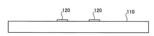
図1は、実施の形態1にかかる光サブアセンブリを示す正面断面図である。実施の形態1にかかる光サブアセンブリ100は、入力された電気信号に応じた光信号を生成して出射するTOSAである。図1に示すように、光サブアセンブリ100は、配線基板110と、接続電極120と、半田バンプ130と、高融点ガラス140と、低融点ガラス150と、LD160と、レンズ部材170と、を備えている。
(Embodiment 1)
FIG. 1 is a front sectional view showing an optical subassembly according to the first embodiment. The
配線基板110は、たとえばアルミナ(酸化アルミニウム)などのセラミック基板である。接続電極120は、配線基板110とLD160とを接続する電極であり、配線基板110上に形成されている。半田バンプ130(第二低融点部材)は、接続電極120よりも融点が低く、接続電極120上に配置されている。半田バンプ130は金とすずの合金(半田金属)である。
高融点ガラス140(高融点部材)は、配線基板110上に凸状に形成されている。高融点ガラス140は、配線基板110との相対位置を決めて配線基板110上に形成されている。高融点ガラス140はたとえばシリカガラスである。低融点ガラス150(低融点部材)は、高融点ガラス140よりも融点が低いガラス部材である。低融点ガラス150は、高融点ガラス140上に配置されている。低融点ガラス150は、たとえば燐やボロンなどの不純物を添加したシリカガラスである。
The high melting point glass 140 (high melting point member) is formed in a convex shape on the
LD160(光電変換素子)は、半田バンプ130を介して接続電極120に接続されている。LD160は、発光部161と発光部161に電気信号を伝送する電極162とを有している。LD160の電極162は半田バンプ130上に配置されている。また、LD160は、配線基板110、高融点ガラス140、低融点ガラス150およびレンズ部材170によって気密封止されている。
The LD 160 (photoelectric conversion element) is connected to the
レンズ部材170は、高融点ガラス140に合わせた形状の突起部171とレンズ部172とを有する。高融点ガラス140に合わせた突起部171の形状とは、突起部171を高融点ガラス140上に配置した場合に、互いの接合面の形状がほぼ一致する形状である。特に、この接合面の形状が完全に一致する形状に突起部171を形成することで、後述するセルフアライメント効果による位置決めの精度を高めることができる。
The
たとえば、高融点ガラス140と突起部171とを同半径の円環状に形成し、互いの接合面を同半径の円形状とする。また、レンズ部材170は、突起部171を低融点ガラス150上に配置して高融点ガラス140および配線基板110に対して固定される。また、レンズ部材170は、低融点ガラス150を溶融させることに起因するセルフアライメント効果によって高融点ガラス140に対して位置決めされた状態で、高融点ガラス140と接合されている。
For example, the
また、突起部171とレンズ部172とを備えるレンズ部材170を一体の透過部材によって構成することで、突起部171にも光透過性を持たせることができる。また、レンズ部材170には、低融点ガラス150よりも高い融点(たとえば高融点ガラス140と同程度の融点)を有する透過部材を用いる。レンズ部材170のレンズ部172の光軸173は、LD160の発光部161の光軸163と一致している。
In addition, by forming the
図2は、実施の形態1にかかる光サブアセンブリの配線基板およびLDを示す一部透過平面図である。図1は図2のAA’断面図である。図2に示すように、発光部161はLD160の表面に設けられ、電極162はLD160の裏面に4つ設けられている。4つの電極162は、LD160の裏面の四隅に、発光部161の光軸163からの距離が互いに等しくなるように設けられている。
FIG. 2 is a partially transparent plan view showing the wiring board and LD of the optical subassembly according to the first embodiment. 1 is a cross-sectional view taken along the line AA 'of FIG. As shown in FIG. 2, the
接続電極120は、配線基板110上に4つ形成されている。4つの接続電極120は、4つの電極162に対応した位置にそれぞれ形成され、それぞれ半田バンプ130を介してLD160の電極162と接合している。高融点ガラス140は、配線基板110上で接続電極120を囲む円環状(ドーナツ型)に形成されている。
Four
また、高融点ガラス140は、4つの接続電極120の中心点を中心とした円環状(半径をrとする)に形成されている。接続電極120に接続されたLD160の光軸163は4つの接続電極120の中心点を通過するため、高融点ガラス140は、LD160の光軸163を中心とした円環状に形成される。
The
なお、ここでは、LD160の4つの電極162の形状は、それぞれ4つの接続電極120に合わせた形状である。LD160の4つの電極162は、4つの半田バンプ130を溶融させることに起因するセルフアライメント効果によってそれぞれ4つの接続電極120に対して位置決めされた状態で接合されている。
Here, the shape of the four
図3は、実施の形態1にかかる光サブアセンブリのレンズ部材を示す一部透過平面図である。図3に示すように、レンズ部材170のレンズ部172はレンズ部材170の表面に設けられ、突起部171はレンズ部材170の裏面に設けられている。レンズ部材170の突起部171は、高融点ガラス140に合わせた円環状に形成されている。また、レンズ部材170の突起部171と光軸173との相対位置は、接続電極120と高融点ガラス140との相対位置に応じて決められる。
FIG. 3 is a partially transparent plan view illustrating the lens member of the optical subassembly according to the first embodiment. As shown in FIG. 3, the
ここでは、高融点ガラス140は4つの接続電極120の中心点を中心とした半径rの円環状(図2参照)であるため、レンズ部材170の突起部171は、レンズ部材170の光軸173を中心とした半径rの円環状に形成されている。このため、高融点ガラス140とレンズ部材170の突起部171とを位置を合わせて接合することで、4つの接続電極120の中心点を通過する発光部161の光軸163と、レンズ部172の光軸173と、が一致する。
Here, since the
図4は、実施の形態1にかかる光サブアセンブリの製造工程の一例を示すフローチャートである。図4に示すように、まず、LD160の電極162が配置される配線基板110上の位置に接続電極120を形成する(ステップS401)。つぎに、ステップS401によって形成した接続電極120との相対位置を決めて配線基板110上に高融点ガラス140を形成する(ステップS402)。
FIG. 4 is a flowchart of an example of the manufacturing process of the optical subassembly according to the first embodiment. As shown in FIG. 4, first, the
つぎに、ステップS402によって形成した高融点ガラス140上に低融点ガラス150を配置する(ステップS403)。つぎに、ステップS401によって形成した接続電極120上に半田バンプ130を配置する(ステップS404)。つぎに、ステップS404によって配置した半田バンプ130上にLD160を配置する(ステップS405)。
Next, the low
つぎに、半田バンプ130を溶融させることによって配線基板110に対してLD160を位置決めする(ステップS406)。つぎに、半田バンプ130を冷却することによって配線基板110に対してLD160を固定する(ステップS407)。つぎに、ステップS403によって配置した低融点ガラス150上にレンズ部材170を配置する(ステップS408)。
Next, the
つぎに、低融点ガラス150を溶融させることによって配線基板110に対してレンズ部材170を位置決めする(ステップS409)。つぎに、低融点ガラス150を冷却することによって配線基板110に対してレンズ部材170を固定し(ステップS410)、一連の光サブアセンブリ100の製造工程を終了する。
Next, the
図5は、図4のステップS401に対応した工程図である。ここでは、LD160の4つの電極162に対応した配線基板110上の位置に接続電極120を4つ形成する。図6〜図9は、図4のステップS402およびS403に対応した工程図(その1)〜(その4)である。まず、図6に示すように、化学的気相堆積法などによって高融点ガラス140の層、低融点ガラス150の層の順に配線基板110上に成膜する。
FIG. 5 is a process diagram corresponding to step S401 in FIG. Here, four
つぎに、図7に示すように、エッチング後の高融点ガラス140と接続電極120との相対位置が上述した位置となるように、低融点ガラス150上にフォトレジスト710を円環状にパターニングする。つぎに、図8に示すように、化学的イオンエッチング法などによって、高融点ガラス140および低融点ガラス150のうちフォトレジスト710がパターニングされていない部分を除去する。
Next, as shown in FIG. 7, a
つぎに、図9に示すように、酵素プラズマを用いた灰化および洗浄などによってフォトレジスト710を除去する。これによって、配線基板110上に高融点ガラス140および低融点ガラス150が形成される。図10〜図12は、図4のステップS404に対応した工程図(その1)〜(その3)である。図10に示すように、配線基板110の表面のうち接続電極120を除いた部分にフォトレジスト1010をパターニングする。
Next, as shown in FIG. 9, the
つぎに、図11に示すように、真空蒸着法などによって半田金属130aの層を成膜する。つぎに、図12に示すように、アセトンなどの有機溶剤に浸透させるリフトオフ法などによって、フォトレジスト1010およびフォトレジスト1010上の半田金属130aを除去する。これによって、接続電極120上に残った半田金属130aを半田バンプ130として説明する。
Next, as shown in FIG. 11, a layer of
図13は、図4のステップS405に対応した工程図である。図13に示すように、半田バンプ130上にLD160の電極162を配置する。この工程においては、LD160の電極162は半田バンプ130上に正確に位置決めされている必要はなく、電極162が半田バンプ130上に乗っている状態にすればよい。
FIG. 13 is a process diagram corresponding to step S405 in FIG. As shown in FIG. 13, the
図14は、図4のステップS406およびS407に対応した工程図である。ステップS406では、たとえば配線基板110および配線基板110上の素子全体を300℃程度に加熱して半田バンプ130のみを溶融させる。この場合、半田バンプ130を除く全ての素子の融点を300℃よりも高くしておく。半田バンプ130を溶融させると、図14に示すように、溶融した半田バンプ130の表面張力に起因するセルフアライメント効果によって、LD160の電極162が接続電極120に対して一意に位置決めされる。
FIG. 14 is a process diagram corresponding to steps S406 and S407 of FIG. In step S406, for example, the
このため、LD160を配線基板110の所定位置に位置決めすることができる。つぎに、溶融した半田バンプ130を冷却して凝固させることで、配線基板110上に位置決めした状態でLD160を固定することができる。溶融した半田バンプ130の冷却は、たとえば自然冷却により行う。
For this reason, the
図15は、図4のステップS408に対応した工程図である。図15に示すように、低融点ガラス150上にレンズ部材170の突起部171を配置する。この工程においては、突起部171は低融点ガラス150上に正確に位置決めされている必要はなく、突起部171が低融点ガラス150上に乗っている状態にすればよい。
FIG. 15 is a process diagram corresponding to step S408 in FIG. As shown in FIG. 15, the
図4のステップS409およびS410に対応した工程図は、図1と同様であるため図示を省略する。低融点ガラス150を溶融させるために、たとえば低融点ガラス150にレーザを照射する。低融点ガラス150に照射するレーザには、たとえばフェムト秒レーザを用いる。これにより、低融点ガラス150を瞬間的に加熱することができる。
The process diagram corresponding to steps S409 and S410 in FIG. 4 is the same as that in FIG. In order to melt the
また、レンズ部材170の突起部171はレーザを透過させる光透過性を有する。これにより、図15の符号1510に示すように、突起部171を介して低融点ガラス150にレーザを照射することで低融点ガラス150の温度を上昇させ、低融点ガラス150を溶融させることができる。
Further, the
このとき、レーザのビーム焦点を低融点ガラス150に合わせることで、非線形な光吸収現象(二光子吸収)により、低融点ガラス150の温度を局部的に上昇させることができる。このため、半田バンプ130、高融点ガラス140、LD160、レンズ部材170などの低融点ガラス150周辺の素子を損傷させることなく低融点ガラス150を溶融させることができる。
At this time, by focusing the laser beam on the low-melting
たとえば、低融点ガラス150の円環に沿ってレーザの照射装置を回転させながらレーザを照射することで、低融点ガラス150全体を同時に溶融した状態にすることができる。レーザが照射され溶融した低融点ガラス150が自然冷却により再度固化状態となるまでの時間をΔt、レーザのスポットが低融点ガラス150の円環を回る周期をTとする。
For example, the entire low-melting
この場合、時間Δtよりも周期Tが短くなるように、レーザパルスの照射エネルギー(10〜100nJ/パルス)、パルス発生頻度(1k〜10kパルス/秒)、ビームの移動速度(0.1〜10mm/s)を制御することで、低融点ガラス150全体が同時に溶融した状態とすることができる。また、レーザの照射装置を複数用意して、複数の照射装置を低融点ガラス150の円環に沿って回転させてもよい。
In this case, laser pulse irradiation energy (10 to 100 nJ / pulse), pulse generation frequency (1 k to 10 k pulse / second), beam moving speed (0.1 to 10 mm) so that the period T is shorter than the time Δt. By controlling / s), the entire low-melting
たとえば2つの照射装置を、低融点ガラス150の円環上の互いに離れた位置に設けて同時に回転させることで、1回転毎に低融点ガラス150に対してレーザを2回照射することができる。このため、たとえばビームの移動速度(照射装置の回転速度)を半分にすることができる。なお、低融点ガラス150に対するレーザの照射は乾燥窒素雰囲気中で行うとよい。
For example, by providing two irradiation devices at positions separated from each other on the ring of the low
また、突起部171を介して低融点ガラス150にレーザを照射する場合の、レンズ部材170におけるレーザの入射部174は、突起部171と低融点ガラス150の接合面と平行に形成されている。これにより、入射部174に対してレーザを垂直に入射すると、レーザが低融点ガラス150まで直進するため、低融点ガラス150に対してレーザを精度よく照射することができる。
In addition, the
また、入射部174の表面に無反射コーティングを施してもよい。これにより、入射部174におけるレーザの反射を防ぐことができ、低融点ガラス150に対してレーザを効率よく照射することができる。また、入射部174と、突起部171における低融点ガラス150との接合面と、の距離は、円環状に形成された突起部171の各部分において等しくなるように形成する。これにより、照射装置を回転させながらレーザを低融点ガラス150に照射する場合に、レーザのビーム焦点を一定にしておくことができる。
Further, an antireflective coating may be applied to the surface of the
低融点ガラス150を溶融させると、図1に示すように、溶融した低融点ガラス150の表面張力に起因するセルフアライメント効果によって、レンズ部材170の突起部171が高融点ガラス140に対して一意に位置決めされる。このため、レンズ部材170を配線基板110の所定位置に位置決めし、LD160の光軸163とレンズ部材170の光軸173とを高精度に一致させることができる。
When the low-melting
つぎに、溶融した低融点ガラス150を冷却して凝固させることで、配線基板110上に位置決めした状態でレンズ部材170を固定することができる。溶融した低融点ガラス150の冷却は、たとえば自然冷却により行う。これにより、配線基板110、高融点ガラス140、低融点ガラス150およびレンズ部材170によってLD160が気密封止される。
Next, the
このように、実施の形態1にかかる光サブアセンブリ100の製造方法および光サブアセンブリ100によれば、溶融した低融点ガラス150の表面張力に起因するセルフアライメント効果を利用してレンズ部材170を配線基板110および高融点ガラス140に対して自動的、高精度かつ高速に位置決めできる。このため、光サブアセンブリ100の製造時間を短縮し、光サブアセンブリ100の低コスト化を図ることができる。
As described above, according to the manufacturing method of the
たとえば、実施の形態1にかかる光サブアセンブリ100の製造方法ではレンズ部材170の位置決めと、LD160の気密封止と、を低融点ガラス150の溶融によって同時に行うため、これらの作業時間を低融点ガラス150の溶融および冷却にかかる10秒程度にすることができる。
For example, in the method of manufacturing the
また、LD160を囲む環状にレンズ部材170の突起部171、高融点ガラス140および低融点ガラス150を形成することで、金属キャップを用いることなくレンズ部材170によってLD160を気密封止できる。このため、光サブアセンブリ100を小型化することができる。また、光サブアセンブリ100の接合部を減らすことができ、光サブアセンブリ100を高精度に構成することができる。また、光サブアセンブリ100の部品数を減らし、光サブアセンブリ100の低コスト化を図ることができる。
Further, by forming the
また、レンズ部材170の突起部171に光透過性を持たせ、突起部171を介して低融点ガラス150にレーザを照射することで、容易に低融点ガラス150のみを加熱して溶融させることができる。このため、低融点ガラス150周辺の素子を損傷させることなく低融点ガラス150を溶融させることができる。レンズ部172はレンズの特性として光透過性を有するため、一体の透過部材によりレンズ部材170を形成することで、突起部171に容易に光透過性を持たせることができる。
Further, the
また、低融点ガラス150を円環状に形成し、レーザの照射装置を回転させながら低融点ガラス150にレーザを照射することで、低融点ガラス150全体を効率的に加熱して溶融させることができる。また、回転させるレーザの照射装置を複数設けることで、低融点ガラス150全体をさらに効率的に加熱して溶融させることができる。
Further, the low
また、接続電極120および高融点ガラス140をリソグラフィによって形成することで、接続電極120と高融点ガラス140との相対位置を高精度に決めることができる。さらに、半田バンプ130および低融点ガラス150のセルフアライメント効果を利用することで、接続電極120に対してLD160、高融点ガラス140に対してレンズ部材170を高精度に位置決めすることができる。このため、LD160の光軸163とレンズ部材170の光軸173とを容易かつ高精度に一致させ、光サブアセンブリ100の光学特性を向上させることができる。
Further, by forming the
たとえば、リソグラフィによる接続電極120および高融点ガラス140の位置決め精度は±0.1μm、半田バンプ130によるセルフアライメント効果を利用したLD160位置決め精度は0.5μm以下、低融点ガラス150によるセルフアライメント効果を利用したレンズ部材170の位置決め精度は0.5μm以下となり、これらを合わせた位置合わせ精度は最大で±1.2μmとなる。
For example, the positioning accuracy of the
これにより、レンズ部材170の光軸173とLD160の光軸163との位置決めに要求される光軸調整精度(たとえば±2.5μm以下)を満たすことができる。また、高融点部材および低融点部材に高融点ガラス140および低融点ガラス150などのガラス部材を用いることで、配線基板110とレンズ部材170との接合部分の強度や耐腐食性が向上し、LD160を安定して気密封止することができる。
Thereby, the optical axis adjustment accuracy (for example, ± 2.5 μm or less) required for positioning the
(実施の形態2)
図16は、実施の形態2にかかる光サブアセンブリを示す正面断面図である。図17は、実施の形態2にかかる光サブアセンブリの配線基板およびLDを示す一部透過平面図である。図16および図17において、図1および図2に示した構成と同様の構成については同一の符号を付して説明を省略する。図16は図17のAA’断面図である。
(Embodiment 2)
FIG. 16 is a front sectional view of the optical subassembly according to the second embodiment. FIG. 17 is a partially transparent plan view showing the wiring board and LD of the optical subassembly according to the second embodiment. 16 and 17, the same components as those shown in FIGS. 1 and 2 are denoted by the same reference numerals, and description thereof is omitted. 16 is a cross-sectional view taken along the line AA ′ of FIG.
図16および図17に示すように、実施の形態2にかかる光サブアセンブリ100の配線基板110には、4つ(複数)の高融点ガラス140が点在して形成されている。4つの高融点ガラス140は、ここではそれぞれ円柱形の凸状に形成されている。4つの高融点ガラス140は、配線基板110上に、LD160の光軸163を中心とした半径Rの円周上に等間隔で設けられている。低融点ガラス150は、4つの高融点ガラス140に対応して4つ設けられ、複数の高融点ガラス140上にそれぞれ配置されている。
As shown in FIGS. 16 and 17, four (plurality) of high
また、配線基板110には、4つの高融点ガラス140の他に高融点ガラス1610(第二高融点部材)が形成されている。高融点ガラス1610は、配線基板110上で接続電極120を囲む円環状(ドーナツ型)に形成されている。また、高融点ガラス1610は、4つの接続電極120の中心点を中心とした半径rの円環状に形成されている。高融点ガラス1610はたとえば高融点ガラス140と同じ材質である。
In addition to the four high
また、レンズ部材170の突起部1630はレーザを透過させる光透過性を有する。たとえば、突起部171、レンズ部172および突起部1630を備えるレンズ部材170を一体の透過部材によって構成することで、突起部171および突起部1630に光透過性を持たせることができる。
Further, the
接続電極120に接続されたLD160の発光部161の光軸163は4つの接続電極120の中心点を通過するため、高融点ガラス1610は、LD160の発光部161の光軸163を中心とした円環状に形成される。高融点ガラス1610上には、高融点ガラス1610よりも融点が低い低融点ガラス1620(第三低融点部材)がそれぞれ配置されている。
Since the
低融点ガラス1620はたとえば低融点ガラス150と同じ材質である。レンズ部材170の突起部171は、4つの高融点ガラス140に対応して4つ設けられている。また、レンズ部材170は、4つの突起部171の他に、高融点ガラス1610に合わせた円環状の突起部1630(第二突起部)を有している。
The low
また、レンズ部材170は、4つの突起部171をそれぞれ複数の低融点ガラス150上に配置するとともに、突起部1630を低融点ガラス1620上に配置した状態で配線基板110に対して固定される。また、レンズ部材170は、4つの低融点ガラス150を溶融させることで高融点ガラス140に対して位置決めされている。
In addition, the
図18は、実施の形態2にかかる光サブアセンブリのレンズ部材を示す一部透過平面図である。図18において、図3に示した構成と同様の構成については同一の符号を付して説明を省略する。図18に示すように、レンズ部材170は、4つ高融点ガラス140に合わせて突起部171を4つ有している。4つの突起部171は、高融点ガラス140の円柱形の凸状に合わせて円柱形の凸状に形成されている。また、4つの突起部171は、レンズ部172の光軸173を中心とした半径Rの円周上に等間隔で設けられている。
FIG. 18 is a partially transparent plan view illustrating a lens member of the optical subassembly according to the second embodiment. 18, the same components as those illustrated in FIG. 3 are denoted by the same reference numerals, and description thereof is omitted. As shown in FIG. 18, the
レンズ部材170の突起部1630は、高融点ガラス1610に合わせた円環状に形成されている。また、レンズ部材170の突起部1630とレンズ部172の光軸173との相対位置は、接続電極120と高融点ガラス140との相対位置に応じて決められる。ここでは、レンズ部材170の突起部1630は、レンズ部材170のレンズ部172の光軸173を中心とした半径rの円環状に形成されている。
The
これにより、低融点ガラス150を溶融させることで、4つ高融点ガラス140と4つの突起部171とを位置合わせすることができる。また、溶融した低融点ガラス150を冷却することで、4つ高融点ガラス140と4つの突起部171とを位置合わせした状態で接合して固定することができる。このため、レンズ部172の光軸173と、4つ高融点ガラス140の中心点を通過する発光部161の光軸163と、が一致する。
Thus, the four high
また、低融点ガラス1620を溶融して冷却することで、高融点ガラス1610とレンズ部材170の突起部1630と接合して固定することができる。これにより、配線基板110、高融点ガラス1610、低融点ガラス1620およびレンズ部材170によってLD160を気密封止することができる。
Further, by melting and cooling the low
図19は、実施の形態2にかかる光サブアセンブリの製造工程の一例を示すフローチャートである。図19に示すように、まず、LD160の電極162が配置される配線基板110上の位置に接続電極120を形成する(ステップS1901)。接続電極120の形成については図5に示した工程図の通りであるため詳細な説明を省略する。
FIG. 19 is a flowchart of an example of the manufacturing process of the optical subassembly according to the second embodiment. As shown in FIG. 19, first, the
つぎに、ステップS1901によって形成した接続電極120との相対位置を決めて配線基板110上に高融点ガラス140および1610を形成する(ステップS1902)。つぎに、ステップS1902によって形成した高融点ガラス140および1610上に低融点ガラス150および1620をそれぞれ配置する(ステップS1903)。
Next, relative positions with respect to the
具体的には、図6〜図9に示した工程図において、接続電極120、高融点ガラス140および高融点ガラス1610との相対位置が上述した位置となるように低融点ガラス150上にフォトレジスト710をパターニングすることで、高融点ガラス140および高融点ガラス1610を形成し、低融点ガラス150および低融点ガラス1620を配置することができる。
Specifically, in the process diagrams shown in FIGS. 6 to 9, a photoresist is formed on the low
つぎに、ステップS1901によって形成した接続電極120上にLD160を位置決めして接続する(ステップS1904)。LD160の位置決めおよび接続については、図10〜図14に示した工程図の通りであるため詳細な説明を省略する。つぎに、ステップS1903によって配置した低融点ガラス150上にレンズ部材170を配置する(ステップS1905)。
Next, the
つぎに、低融点ガラス150を溶融させることによって配線基板110に対してレンズ部材170を位置決めする(ステップS1906)。つぎに、低融点ガラス150を冷却することによって配線基板110に対してレンズ部材170を固定する(ステップS1907)。つぎに、低融点ガラス1620を溶融して冷却することで高融点ガラス1610とレンズ部材170の突起部1630と接合し、LD160を気密封止して(ステップS1908)一連の光サブアセンブリ100の製造工程を終了する。
Next, the
図20は、図19のステップS1906およびS1908に対応した工程図である。ステップS1906においては、図20の符号2010に示すように、レンズ部材170の突起部171を介してフェムト秒レーザなどのレーザを低融点ガラス150に照射することで、低融点ガラス150を溶融させる。
FIG. 20 is a process diagram corresponding to steps S1906 and S1908 of FIG. In step S1906, as shown by
ここで、低融点ガラス150は、4つの高融点ガラス140に対応して点在して4つ設けられているため、レーザの照射装置を4つ用いてこれらの低融点ガラス150に対して同時にレーザを照射すれば、これらの低融点ガラス150を同時に溶融させることが容易となる。このため、配線基板110に対してレンズ部材170を高速かつ高精度に位置決めすることができる。
Here, four low-melting
また、ステップS1908においては、符号2020に示すように、突起部1630を介してフェムト秒レーザなどのレーザを低融点ガラス1620に照射することで、低融点ガラス1620を溶融させる。低融点ガラス1620は、円環状に形成されているため、上述した実施の形態1にかかる低融点ガラス150と同様の方法で溶融させることができる。
In step S1908, as indicated by
ここで、ステップS1906によってレンズ部材170の位置決めは済んでいるため、ステップS1908においては位置決めの精度は必要なく、LD160を円環状の低融点ガラス1620で気密封止できればよい。このため、高融点ガラス1630およびレンズ部材170の突起部1630は、高融点ガラス140およびレンズ部材170の突起部171ほど高精度に形成する必要はない。
Here, since the positioning of the
たとえば、低融点ガラス150にレンズ部材170の突起部171を配置したときに、突起部1630が低融点ガラス1620に接触しないように突起部1630を短めに形成しておいてもよい。この場合、突起部1630は、低融点ガラス1620に高精度に合わせた形状でなくてもよい。
For example, when the
そして、ステップS1908において、まず突起部1630に対してレーザを照射して突起部1630を溶融させることで、溶融した突起部1630が自重で低融点ガラス1620に接触するまで垂れ下がるようにする。つぎに、低融点ガラス1620にレーザを照射して溶融させて突起部1630と接合することで、LD160を確実に気密封止することができる。
In step S1908, the
このように、実施の形態2にかかる光サブアセンブリ100の製造方法および光サブアセンブリ100によれば、実施の形態1の効果を奏するとともに、点在させた低融点ガラス150によって精度よくレンズ部材170を位置決めすることができるとともに、円環状に形成した低融点ガラス1620によってLD160を気密封止することができる。
As described above, according to the manufacturing method of the
なお、上述した各実施の形態において、高融点ガラス140などを配線基板110に設けることによって配線基板110上に高融点部材を形成する構成について説明したが、配線基板110自体を高融点の材質にし、たとえば配線基板110上に溝を設けて配線基板110の一部を凸状にすることで配線基板110上に高融点部材を形成してもよい。
In each of the embodiments described above, the configuration in which the high melting point member is formed on the
また、上述した各実施の形態において、光電変換素子としてLD160を接続電極120上に設けることで光サブアセンブリ100をTOSAとして構成する場合について説明したが、LD160に代えてPDを接続電極120上に設けることで、光サブアセンブリ100をROSAとして構成することができる。この場合、レンズ部材170のレンズ部172の光軸173をPDの光軸(PDの受光感度が最も高くなる光路)と一致させる。
In each of the above-described embodiments, the case where the
また、上述した各実施の形態において、高融点部材および低融点部材として高融点ガラス140および低融点ガラス150を用いる構成について説明したが、高融点部材および低融点部材はこれらのガラス部材に限らない。すなわち、高融点部材および低融点部材は、互いに融点が異なり、溶融によって接合が可能な部材であればよい。
Moreover, in each embodiment mentioned above, although the structure which uses the
また、上述した各実施の形態において、接続電極120上に半田バンプ130を配置し、半田バンプ130上にLD160の電極162を配置する方法について説明したが、LD160を位置決めする方法はこれに限らない。たとえば、あらかじめLD160の電極162に半田バンプ130を溶接しておき、接続電極120上に半田バンプ130とLD160とをまとめて配置してもよい。
In each of the above-described embodiments, the method of disposing the
また、上述した実施の形態1において、高融点ガラス140は、配線基板110上で接続電極120を囲む円環状(ドーナツ型)に形成する構成について説明したが、高融点ガラス140の形状は円環に限らない。たとえば、高融点ガラス140は、接続電極120を囲む環状の矩形や、接続電極120を囲む環状の楕円形としてもよい。実施の形態2にかかる高融点ガラス1610についても同様である。
In the first embodiment described above, the
また、上述した実施の形態1において、低融点ガラス150の円環に沿ってレーザの照射装置を回転させながらレーザを照射させる方法について説明したが、レーザの照射方法はこれに限らず、複数の照射装置を低融点ガラス150の円環に沿って並べ、低融点ガラス150全体に同時にレーザを照射してもよい。実施の形態2にかかる低融点ガラス1620についても同様である。
In Embodiment 1 described above, the method of irradiating the laser while rotating the laser irradiation device along the ring of the low-melting
また、上述した実施の形態2において、高融点ガラス140、低融点ガラス150およびレンズ部材170の突起部171をそれぞれ4つずつ設ける構成について説明したが、これらはそれぞれ4つずつに限らない。たとえば、高融点ガラス140が円柱である場合、これらを少なくともそれぞれ2つずつ設けることで、セルフアライメント効果によるレンズ部材170の位置決めを行うことができる。各実施の形態の接続電極120、半田バンプ130およびLD160の電極162についても同様である。
Moreover, in Embodiment 2 mentioned above, although the structure which provides the
また、上述した実施の形態2において、低融点ガラス150に対応してレーザの照射装置を4つ用いてこれらの低融点ガラス150に対してレーザを照射する方法について説明したが、レーザの照射方法はこれに限らず、1つの照射装置を移動させながら4つの低融点ガラス150に対して順次レーザを照射し、4つの低融点ガラス150を同時に溶融させてもよい。
Further, in Embodiment 2 described above, the method of irradiating laser to these
(実施例1)
図21は、本発明の実施例1にかかるOSAアレイを示す正面断面図である。本発明の実施例1にかかる光サブアセンブリ(OSA)アレイ2100は、本発明の実施の形態1にかかる光サブアセンブリ100を複数アレイ状に配置した実施例である。図21に示すように、OSAアレイ2100は、複数の光サブアセンブリ100と、ガイドピン2110と、フェルール2120と、複数の光ファイバ2130と、を備えている。
Example 1
FIG. 21 is a front sectional view showing the OSA array according to Example 1 of the present invention. An optical subassembly (OSA)
複数の光サブアセンブリ100は、上述したようにLD160を備え、TOSAとして構成されている。複数の光サブアセンブリ100はアレイ状に並んでおり、それぞれの配線基板110が一体的に構成されている。複数の光サブアセンブリ100は、上述したセルフアライメント効果を利用して配線基板110に対して位置決めされている。
As described above, the plurality of
ガイドピン2110は、複数の光サブアセンブリ100の一体的に構成された配線基板110に対してフェルール2120を固定する。フェルール2120は、複数の光ファイバ2130を、複数の光サブアセンブリ100のレンズ部材170のそれぞれの光軸173上に位置決めする。フェルール2120は、たとえばMT(Mechanically Transferable)フェルールである。
The guide pins 2110 fix the
光サブアセンブリ100は、LD160によって生成した光信号を光ファイバ2130を介して出射する。また、LD160に代えてPDを備え、光サブアセンブリ100をROSAとして構成した場合、光サブアセンブリ100は、光ファイバ2130を介して受光した光信号を電気信号に変換する。
The
本発明の実施例1にかかるOSAアレイ2100によれば、光サブアセンブリ100のサイズを0.2mm(直径)×0.2mm(高さ)程度にすることができる。このため、複数の光サブアセンブリ100をたとえば0.25mm間隔でアレイ状に実装することができ、光インタコネクトにおいて要求される実装密度を満たすことができる。
According to the
(実施例2)
図22は、本発明の実施例2にかかる光インタコネクト用デバイスを示す正面断面図である。本発明の実施例2にかかる光インタコネクト用デバイス2200は、チップやボード上で光信号を空間伝搬によって伝送する光インタコネクト用デバイスに本発明の実施の形態1にかかる光サブアセンブリ100を適用した実施例である。図22に示すように、光インタコネクト用デバイス2200は、TOSA2210と、ROSA2220と、を備えている。
(Example 2)
FIG. 22 is a front sectional view showing an optical interconnect device according to the second embodiment of the present invention. In the
TOSA2210は、実施の形態1にかかる光サブアセンブリ100においてレンズ部材170を変形させた構成となっている。レンズ部材170は、LD160から垂直に出射された光を直角に反射させる反射ミラー2211を備えている。また、レンズ部材170のレンズ部172は、LD160から出射され反射ミラー2211によって反射した光を通過させる位置に設けられている。
The
レンズ部172の光軸173は、LD160から出射され反射ミラー2211によって反射した光の光路2212(所定光路)と一致している。これにより、LD160から出射された光は、配線基板110に対して水平となってレンズ部172から出射される。TOSA2210およびROSA2220は水平方向に実装され、それぞれの配線基板110は一体的に構成されている。
The
ROSA2220は、実施の形態1にかかる光サブアセンブリ100においてレンズ部材170を変形させ、LD160に代えてPD2221を備えた構成となっている。ROSA2220におけるレンズ部材170のレンズ部172は、TOSA2210から水平に出射された光を通過させる位置に設けられている。レンズ部172の光軸173は、TOSA2210から水平に出射された光の光路2212と一致している。
The
また、レンズ部材170は、レンズ部172を通過した光を直角に全反射させる反射ミラー2222を備えている。反射ミラー2222は、反射させた光の光軸2223がPD2221の光軸と一致する位置に設けられている。これにより、TOSA2210から水平に出射された光は、PD2221によって受光される。このため、光インタコネクト用デバイス2200は、TOSA2210からROSA2220へ、空間伝送によって光信号を伝送することができる。
The
本発明の実施例2にかかる光インタコネクト用デバイス2200によれば、光サブアセンブリ100のサイズを0.2mm(直径)×0.2mm(高さ)程度にすることができる。このため、複数の光サブアセンブリ100をたとえば0.25mm間隔でアレイ状に実装することができ、光インタコネクト用デバイスにおいて要求される実装密度を満たすことができる。また、配線基板110に対してTOSA2210とROSA2220とのLD160およびレンズ部材170を精度よく位置決めできるため、光の伝送精度を向上させることができる。
According to the
(実施例3)
図23は、本発明の実施例3にかかるWDM発振器を示す正面断面図である。本発明の実施例3にかかる波長多重光(WDM:Wavelength Division Multiplexing)発振器2300は、異なる波長の複数の光を生成し、生成したそれぞれの光を多重化して出射する波長多重光発振器に本発明の実施の形態1にかかる光サブアセンブリ100を適用した実施例である。
Example 3
FIG. 23 is a front sectional view showing a WDM oscillator according to the third embodiment of the present invention. A wavelength division multiplexing (WDM)
図23に示すように、WDM発振器2300は、複数のTOSA2310,2320,2330,2340と、反射部材2350と、を備えている。複数のTOSA2310,2320,2330,2340は、それぞれ波長λ1〜波長4の光信号を出射する。TOSA2310は、上述したTOSA2210において、LD160が波長λ1の光を発振する構成である。
As shown in FIG. 23, the
TOSA2310は、λ1の光信号をTOSA2320へ出射する。TOSA2310,2320,2330,2340は水平方向に実装され、それぞれの配線基板110は一体的に構成されている。TOSA2320は、上述したTOSA2210において、反射ミラー2211が波長選択ミラーとなっており、LD160が波長λ2の光を発振する構成である。
The
TOSA2320の反射ミラー2211は、波長λ1の光を通過させ、波長λ2の光を反射させる。TOSA2320の反射ミラー2211は、TOSA2310から出射された光信号を通過させる位置で、TOSA2320のLD160から発振された光信号を反射させる位置に設けられている。
The
これにより、TOSA2310から出射されてTOSA2320の反射ミラー2211を通過した波長λ1の光信号と、TOSA2320のLD160から発振されて反射ミラー2211によって反射した波長λ2の光信号と、が重なり合って多重化される。TOSA2320は、多重化した光信号(λ1,λ2)をTOSA2330へ出射する。
As a result, the optical signal having the wavelength λ1 emitted from the
TOSA2330およびTOSA2340は、それぞれのLD160が発振する光信号の波長を除いてTOSA2320と同様の構成である。TOSA2330は、TOSA2320から出射された光信号(λ1,λ2)に波長λ3の光信号を多重化し、多重化した光信号(λ1〜λ3)をTOSA2340へ出射する。TOSA2340は、TOSA2330から出射された光信号(λ1〜λ3)に波長λ4の光信号を多重化し、多重化した光信号(λ1〜λ4)を反射部材2350へ出射する。
The
反射部材2350は、上述したTOSA2210において、LD160を省いた構成である。反射部材2350は、TOSA2340から出射された光信号(λ1〜λ4)を反射ミラー2211によって直角に全反射させ、配線基板110とは反対側に出射する。これにより、WDM発振器2300は、波長λ1〜λ4の光信号を多重化した光信号を出射することができる。
The reflecting
本発明の実施例3にかかるWDM発振器2300によれば、光サブアセンブリ100のそれぞれの小型化を図ることで複数の光サブアセンブリ100をアレイ状に高密度に実装することができ、WDM発振器としての小型化を図ることができる。また、光サブアセンブリ100をアレイ状に高密度に実装することができるため、光サブアセンブリ100毎の光路長差に起因する光信号の波長成分毎の誤差を小さくすることができる。
According to the
また、TOSA2310,2320,2330および2340のLD160およびレンズ部材170を配線基板110に対して精度よく位置決めできるため、それぞれの波長成分の光信号を精度よく多重化することができる。このため、高精度な波長多重光信号を出力することができる。
In addition, since the
(実施例4)
図24は、本発明の実施例4にかかる受信回路を示す概略平面図である。本発明の実施例4にかかる受信回路2400は、差動位相変調(DPSK:Differential Phase Shift Keying)がなされた光信号を分岐し、分岐信号の一方に1シンボル分の遅延を与えて干渉させるDPSK受信回路に本発明の実施の形態1にかかる光サブアセンブリ100を適用した実施例である。
Example 4
FIG. 24 is a schematic plan view illustrating a receiving circuit according to the fourth embodiment of the present invention. The receiving
図24に示すように、受信回路2400は、全反射ミラー2410と、ハーフミラー2420と、全反射ミラー2430と、全反射ミラー2440と、ハーフミラー2450と、PD2460と、PD2470と、を備えるマッハツェンダ型干渉計である。受信回路2400が備える各素子はそれぞれ光サブアセンブリ100を変形した構成であり、それぞれの配線基板110は一体的に構成されている。
As shown in FIG. 24, the receiving
全反射ミラー2410は、差動位相変調がなされた光信号を反射させてハーフミラー2420へ出射する。ハーフミラー2420は、全反射ミラー2410から出射された光信号の一部を反射させて全反射ミラー2430へ出射し、全反射ミラー2410から出射された光信号の一部を通過させてハーフミラー2450へ出射する。
全反射ミラー2430および全反射ミラー2440は、ハーフミラー2420から出射された光信号を迂回させて1シンボル分の遅延を与える迂回経路を構成する。全反射ミラー2430および全反射ミラー2440は、ハーフミラー2420から出射された光信号に遅延を与えてハーフミラー2450へ出射する。
ハーフミラー2450は、ハーフミラー2420から出射された光信号の一部を反射させてPD2460へ出射し、ハーフミラー2420から出射された光信号の一部を通過させてPD2470へ出射する。また、ハーフミラー2450は、全反射ミラー2440から出射された光信号の一部を反射させてPD2470へ出射し、全反射ミラー2440から出射された光信号の一部を通過させてPD2460へ出射する。
The
PD2460およびPD2470は、ハーフミラー2450から出射された光信号をそれぞれ受光して電気信号に変換する。PD2460が受光した光信号とPD2470が受光した光信号とは正相・逆相の関係にある。受信回路2400は、これらの正相・逆相の関係にある光信号をバランス受信することで、差動位相変調がなされた光信号を復調することができる。
図25は、本発明の実施例4にかかる受信回路を示す正面断面図である。図25は図24のAA’断面図である。図25に示すように、全反射ミラー2410は、上述した反射部材2350(図23参照)と同様の構成である。図示しないが、全反射ミラー2430および全反射ミラー2440は、上述した反射部材2350において、配線基板110と平行に出射された光を配線基板110と平行のまま直角に反射させるように反射ミラー2211を変形した構成である。
FIG. 25 is a front sectional view showing a receiving circuit according to the fourth embodiment of the present invention. 25 is a cross-sectional view taken along the line AA 'of FIG. As shown in FIG. 25, the
ハーフミラー2420およびハーフミラー2450は、上述したTOSA2210において、反射ミラー2211に代えてハーフミラー2510を備え、LD160を省いた構成である。PD2470は、上述したROSA2220(図22参照)と同様の構成である。図示しないが、PD2460も上述したROSA2220と同様の構成である。
The
本発明の実施例4にかかる受信回路2400によれば、マッハツェンダ型干渉計の各素子に光サブアセンブリ100の構成の変形例を適用することで、マッハツェンダ型干渉計の各素子を高密度に実装することができる。このため、小型のマッハツェンダ型干渉計を構成することができる。
According to the
また、全反射ミラー2410、ハーフミラー2420、全反射ミラー2430、全反射ミラー2440、ハーフミラー2450、PD2460およびPD2470の全ての素子を配線基板110に対して精度よく位置決めできるため、高精度なマッハツェンダ型干渉計を構成することができる。このため、差動位相変調がなされた光信号を高精度に復調することができる。
In addition, since all the elements of the
なお、上述した各実施例においては、本発明の実施の形態1にかかる光サブアセンブリ100を適用する例について説明したが、上述した各実施例に本発明の実施の形態2にかかる光サブアセンブリ100を適用することもできる。
In each of the above-described examples, the example in which the
以上説明したように、この発明にかかる光サブアセンブリの製造方法、光サブアセンブリによれば、光サブアセンブリの小型化を図りつつ、光サブアセンブリの低コスト化を図ることができる。また、この発明にかかる光サブアセンブリの製造方法、光サブアセンブリをOSAアレイ、光インタコネクト用デバイス、WDM発振器および受信回路に適用することで、OSAアレイ、光インタコネクト用デバイス、WDM発振器および受信回路の製造時間短縮、小型化および高精度化を図ることができる。 As described above, according to the optical subassembly manufacturing method and the optical subassembly according to the present invention, it is possible to reduce the cost of the optical subassembly while reducing the size of the optical subassembly. Also, by applying the optical subassembly manufacturing method and the optical subassembly according to the present invention to an OSA array, an optical interconnect device, a WDM oscillator, and a receiving circuit, the OSA array, the optical interconnect device, the WDM oscillator, and the reception Circuit manufacturing time can be shortened, miniaturized, and highly accurate.
以上のように、この発明にかかる光サブアセンブリの製造方法および光サブアセンブリは、サーバシステムやネットワーク装置の光インタコネクト、光インタコネクト用デバイス、WDM発振器および受信回路などに有用であり、特に、光サブアセンブリの高密度の実装が要求される場合に適している。 As described above, the optical subassembly manufacturing method and the optical subassembly according to the present invention are useful for an optical interconnect of a server system or a network device, an optical interconnect device, a WDM oscillator, a receiving circuit, and the like. Suitable when high density mounting of optical subassemblies is required.
上述した実施の形態に関し、さらに以下の付記を開示する。 The following additional notes are disclosed with respect to the embodiment described above.
(付記1)接続電極と凸状の高融点ガラスとを互いの相対位置を決めて配線基板上に形成する形成工程と、
前記接続電極上に光電変換素子を位置決めして接続する位置決め工程と、
前記高融点ガラス上に前記高融点ガラスよりも融点が低い低融点ガラスを配置する配置工程と、
前記高融点ガラスに合わせた形状の突起部とレンズ部とを有し、前記突起部と前記レンズ部の光軸との相対位置が前記接続電極と前記高融点ガラスとの相対位置に応じて決められたレンズ部材の前記突起部を前記低融点ガラス上に配置して固定する固定工程と、を含み、
前記固定工程では、前記低融点ガラスを溶融させることで前記高融点ガラスに対して前記レンズ部材を位置決めすることを特徴とする光サブアセンブリの製造方法。
(Appendix 1) A forming step of forming a connection electrode and a convex refractory glass on a wiring board by determining relative positions of each other;
A positioning step of positioning and connecting the photoelectric conversion element on the connection electrode;
An arrangement step of arranging a low melting point glass having a lower melting point than the high melting point glass on the high melting point glass,
The projection has a shape matching the high melting point glass and a lens portion, and the relative position between the projection and the optical axis of the lens portion is determined according to the relative position between the connection electrode and the high melting point glass. Fixing the projecting portion of the lens member placed and fixed on the low-melting glass,
In the fixing step, the lens member is positioned with respect to the high melting point glass by melting the low melting point glass.
(付記2)前記光電変換素子は、光電変換部と前記光電変換部に接続された電極とを有し、前記光電変換部の光軸と前記電極との相対位置は所定の位置に決められており、
前記位置決め工程は、前記配線電極よりも融点が低い第二低融点ガラスを前記配線電極上に配置する第二配置工程と、前記光電変換素子の前記電極を前記第二低融点ガラス上に配置して固定する固定工程と、を含み、
前記固定工程では、前記第二低融点ガラスを溶融させることで前記配線電極に対して前記光電変換素子を位置決めすることを特徴とする付記1に記載の光サブアセンブリの製造方法。
(Additional remark 2) The said photoelectric conversion element has a photoelectric conversion part and the electrode connected to the said photoelectric conversion part, and the relative position of the optical axis of the said photoelectric conversion part and the said electrode is decided to the predetermined position. And
In the positioning step, the second low melting point glass having a lower melting point than the wiring electrode is disposed on the wiring electrode, and the electrode of the photoelectric conversion element is disposed on the second low melting point glass. Fixing process, and
The method of manufacturing an optical subassembly according to appendix 1, wherein, in the fixing step, the photoelectric conversion element is positioned with respect to the wiring electrode by melting the second low-melting glass.
(付記3)前記形成工程では、前記接続電極を囲む環状に前記高融点ガラスを形成し、
前記レンズ部材の前記突起部は前記高融点ガラスに合わせた環状に形成され、
前記固定工程では、前記配線基板、前記高融点ガラス、前記低融点ガラスおよび前記レンズ部材によって前記光電変換素子を気密封止することを特徴とする付記1に記載の光サブアセンブリの製造方法。
(Appendix 3) In the forming step, the refractory glass is formed in an annular shape surrounding the connection electrode,
The protrusion of the lens member is formed in an annular shape that matches the high melting point glass,
2. The method of manufacturing an optical subassembly according to appendix 1, wherein in the fixing step, the photoelectric conversion element is hermetically sealed by the wiring substrate, the high melting point glass, the low melting point glass, and the lens member.
(付記4)前記形成工程では、前記配線基板上に複数の前記高融点ガラスを点在して形成し、
前記配置工程では、前記複数の高融点ガラスに複数の前記低融点ガラスをそれぞれ配置し、
前記レンズ部材は、前記複数の高融点ガラスに合わせた複数の前記突起部を有することを特徴とする付記1に記載の光サブアセンブリの製造方法。
(Appendix 4) In the forming step, a plurality of the high melting point glasses are scattered on the wiring substrate,
In the arrangement step, the plurality of low-melting glasses are arranged on the plurality of high-melting glasses,
2. The method of manufacturing an optical subassembly according to appendix 1, wherein the lens member has a plurality of the protrusions that match the plurality of high melting point glasses.
(付記5)前記接続電極を囲む環状の高融点ガラスを前記配線基板上に形成する第二形成工程と、
前記第二高融点ガラス上に前記第二高融点ガラスよりも融点が低い第三低融点ガラスを配置する第二配置工程と、をさらに含み、
前記レンズ部材は、前記第二高融点ガラスに合わせた環状の第二突起部をさらに有し、
前記固定工程では、前記レンズ部材を位置決めした後、前記第二低融点ガラスを溶融させることで前記第二高融点ガラスと前記第二突起部とを接合し、前記配線基板、前記第二高融点ガラス、前記第二低融点ガラスおよび前記レンズ部材によって前記光電変換素子を気密封止することを特徴とする付記4に記載の光サブアセンブリの製造方法。
(Additional remark 5) The 2nd formation process which forms the cyclic | annular high melting point glass surrounding the said connection electrode on the said wiring board,
A second disposing step of disposing a third low melting point glass having a melting point lower than that of the second high melting point glass on the second high melting point glass,
The lens member further includes an annular second protrusion matched to the second refractory glass,
In the fixing step, after positioning the lens member, the second low melting glass is melted to join the second high melting glass and the second protrusion, and the wiring board, the second high melting point The method of manufacturing an optical subassembly according to appendix 4, wherein the photoelectric conversion element is hermetically sealed with glass, the second low-melting glass, and the lens member.
(付記6)前記レンズ部材の前記突起部はレーザを透過させる光透過性を有し、
前記固定工程では、前記突起部を介して前記低融点ガラスにレーザを照射することによって前記低融点ガラスを溶融させることを特徴とする付記1に記載の光サブアセンブリの製造方法。
(Additional remark 6) The said projection part of the said lens member has the light transmittance which permeate | transmits a laser,
2. The method of manufacturing an optical subassembly according to claim 1, wherein, in the fixing step, the low-melting glass is melted by irradiating the low-melting glass with a laser through the protrusion.
(付記7)前記形成工程では、前記高融点ガラスおよび前記低融点ガラスを前記接続電極を囲む環状に形成し、
前記レンズ部材の前記突起部は前記高融点ガラスに合わせた環状に形成され、
前記固定工程では、前記レーザの照射装置を前記低融点ガラスに合わせた円環状に回転しながら前記突起部を介して前記低融点ガラスにレーザを照射することを特徴とする付記6に記載の光サブアセンブリの製造方法。
(Appendix 7) In the forming step, the high melting point glass and the low melting point glass are formed in an annular shape surrounding the connection electrode,
The protrusion of the lens member is formed in an annular shape that matches the high melting point glass,
7. The light according to appendix 6, wherein, in the fixing step, the low-melting glass is irradiated with the laser through the protrusion while rotating the laser irradiation device in an annular shape matching the low-melting glass. Subassembly manufacturing method.
(付記8)前記レーザはフェムト秒レーザであることを特徴とする付記6に記載の光サブアセンブリの製造方法。 (Supplementary note 8) The method of manufacturing an optical subassembly according to supplementary note 6, wherein the laser is a femtosecond laser.
(付記9)前記形成工程では、前記接続電極および前記高融点ガラスをリソグラフィによって形成することを特徴とする付記1に記載の光サブアセンブリの製造方法。 (Additional remark 9) The said formation process WHEREIN: The said connection electrode and the said high melting point glass are formed by lithography, The manufacturing method of the optical subassembly of Additional remark 1 characterized by the above-mentioned.
(付記10)前記高融点ガラスおよび前記低融点ガラスはシリカガラスであり、前記低融点ガラスは前記シリカガラスに不純物を添加することで前記高融点ガラスよりも融点が低いことを特徴とする付記1に記載の光サブアセンブリの製造方法。 (Appendix 10) The high melting point glass and the low melting point glass are silica glasses, and the low melting point glass has an melting point lower than that of the high melting point glass by adding impurities to the silica glass. The manufacturing method of the optical subassembly as described in 2.
(付記11)配線基板上に形成される接続電極と、
前記接続電極との相対位置を決めて前記配線基板上に形成される凸状の高融点ガラスと、
前記接続電極上に位置決めして接続される光電変換素子と、
前記高融点ガラス上に配置され前記高融点ガラスよりも融点が低い低融点ガラスと、
前記高融点ガラスに合わせた形状の突起部とレンズ部とを有し、前記突起部と前記レンズ部の光軸との相対位置が前記接続電極と前記高融点ガラスとの相対位置に応じて決められ、前記突起部を前記低融点ガラス上に配置して固定されるレンズ部材と、を備え、
前記レンズ部材は、前記低融点ガラスを溶融させることで前記高融点ガラスに対して位置決めされることを特徴とする光サブアセンブリ。
(Appendix 11) A connection electrode formed on the wiring board;
A convex refractory glass formed on the wiring board by determining a relative position with the connection electrode;
A photoelectric conversion element positioned and connected on the connection electrode;
A low-melting glass disposed on the high-melting glass and having a lower melting point than the high-melting glass;
The projection has a shape matching the high melting point glass and a lens portion, and the relative position between the projection and the optical axis of the lens portion is determined according to the relative position between the connection electrode and the high melting point glass. A lens member that is disposed and fixed on the low-melting-point glass.
The optical subassembly according to claim 1, wherein the lens member is positioned with respect to the high melting point glass by melting the low melting point glass.
(付記12)前記高融点ガラスは、前記接続電極を囲む環状に形成され、
前記レンズ部材の前記突起部は、前記高融点ガラスに合わせた環状に形成され、
前記光電変換素子は、前記配線基板、前記高融点ガラス、前記低融点ガラスおよび前記レンズ部材によって気密封止されることを特徴とする付記11に記載の光サブアセンブリ。
(Supplementary note 12) The high melting point glass is formed in an annular shape surrounding the connection electrode,
The protrusion of the lens member is formed in an annular shape that matches the refractory glass,
The optical subassembly according to appendix 11, wherein the photoelectric conversion element is hermetically sealed by the wiring board, the high melting point glass, the low melting point glass, and the lens member.
(付記13)前記光電変換素子から出射される光を所定光路へ反射させ、または前記所定光路から出射された光を前記光電変換素子の光軸へ反射させるミラーをさらに備え、
前記レンズ部材の前記レンズ部の光軸は前記所定光路と一致していることを特徴とする付記11に記載の光サブアセンブリ。
(Additional remark 13) The mirror which reflects the light radiate | emitted from the said photoelectric conversion element to a predetermined optical path, or reflects the light radiate | emitted from the said predetermined optical path to the optical axis of the said photoelectric conversion element, is further provided.
The optical subassembly according to appendix 11, wherein an optical axis of the lens portion of the lens member coincides with the predetermined optical path.
(付記14)前記光電変換素子が光信号を発振する発光素子であり、前記光電変換素子によって発振された光信号を前記レンズ部から出射する付記13に記載の光サブアセンブリと、
前記光電変換素子が光信号を受光して電気信号に変換する受光素子であり、前記光サブアセンブリから出射された光信号を受光する付記13に記載の光サブアセンブリと、
を備えることを特徴とする光インタコネクト用デバイス。
(Supplementary note 14) The optical subassembly according to supplementary note 13, wherein the photoelectric conversion element is a light emitting element that oscillates an optical signal, and the optical signal oscillated by the photoelectric conversion element is emitted from the lens unit;
The optical subassembly according to appendix 13, wherein the photoelectric conversion element is a light receiving element that receives an optical signal and converts the optical signal into an electrical signal, and receives the optical signal emitted from the optical subassembly;
An optical interconnect device comprising:
(付記15)付記13に記載の光サブアセンブリを複数備え、
前記複数の光サブアセンブリのそれぞれの前記光電変換素子は互いに異なる波長の光信号を発振する発光素子であり、
前記複数の光サブアセンブリのそれぞれの前記ミラーは、対応する前記光サブアセンブリの前記発光素子が発振する光信号を前記所定光路へ反射させ、他の前記光サブアセンブリから出射された光信号を通過させて前記反射させた光信号と多重化する波長選択ミラーであることを特徴とするWDM発振器。
(Supplementary note 15) A plurality of optical subassemblies according to supplementary note 13,
Each of the photoelectric conversion elements of the plurality of optical subassemblies is a light emitting element that oscillates optical signals having different wavelengths.
Each mirror of the plurality of optical subassemblies reflects an optical signal oscillated by the light emitting element of the corresponding optical subassembly to the predetermined optical path, and passes an optical signal emitted from another optical subassembly. And a wavelength selective mirror that multiplexes with the reflected optical signal.
(付記16)付記13に記載の光サブアセンブリを2つ備え、差動位相変調がなされた光信号を受信して復調する受信回路であって、
前記光電変換素子が光信号を受光して電気信号に変換する受光素子であり、
前記2つの光サブアセンブリは、前記光信号に含まれる正相信号と逆相信号とをバランス受信することを特徴とする受信回路。
(Supplementary note 16) A reception circuit that includes two optical subassemblies according to supplementary note 13, and that receives and demodulates an optical signal subjected to differential phase modulation,
The photoelectric conversion element is a light receiving element that receives an optical signal and converts it into an electrical signal,
The receiving circuit, wherein the two optical subassemblies receive a normal phase signal and a negative phase signal included in the optical signal in a balanced manner.
100 光サブアセンブリ
110 配線基板
120 接続電極
130 半田バンプ
140,1610 高融点ガラス
150,1620 低融点ガラス
160 LD
161 発光部
162 電極
163,173 光軸
170 レンズ部材
171,1630 突起部
172 レンズ部
710,1010 フォトレジスト
2100 OSAアレイ
2110 ガイドピン
2120 フェルール
2130 光ファイバ
2200 光インタコネクト用デバイス
2210,2310,2320,2330,2340 TOSA
2211,2222 反射ミラー
2220 ROSA
2300 WDM発振器
2350 反射部材
2400 受信回路
2410,2430,2440 全反射ミラー
2420,2450 ハーフミラー
DESCRIPTION OF
161
2211, 222
2300
Claims (10)
前記接続電極上に光電変換素子を位置決めして接続する位置決め工程と、
前記高融点ガラス上に前記高融点ガラスよりも融点が低い低融点ガラスを配置する配置工程と、
前記高融点ガラスに合わせた形状の突起部とレンズ部とを有し、前記突起部と前記レンズ部の光軸との相対位置が前記接続電極と前記高融点ガラスとの相対位置に応じて決められたレンズ部材の前記突起部を前記低融点ガラス上に配置して固定する固定工程と、を含み、
前記固定工程では、前記低融点ガラスを溶融させることで前記高融点ガラスに対して前記レンズ部材を位置決めすることを特徴とする光サブアセンブリの製造方法。Forming a connection electrode and a convex refractory glass on a wiring board by deciding relative positions of each other;
A positioning step of positioning and connecting the photoelectric conversion element on the connection electrode;
An arrangement step of arranging a low melting point glass having a lower melting point than the high melting point glass on the high melting point glass,
The projection has a shape matching the high melting point glass and a lens portion, and the relative position between the projection and the optical axis of the lens portion is determined according to the relative position between the connection electrode and the high melting point glass. Fixing the projecting portion of the lens member placed and fixed on the low-melting glass,
In the fixing step, the lens member is positioned with respect to the high melting point glass by melting the low melting point glass.
前記位置決め工程は、前記配線電極よりも融点が低い第二低融点ガラスを前記配線電極上に配置する第二配置工程と、前記光電変換素子の前記電極を前記第二低融点ガラス上に配置して固定する固定工程と、を含み、
前記固定工程では、前記第二低融点ガラスを溶融させることで前記配線電極に対して前記光電変換素子を位置決めすることを特徴とする請求項1に記載の光サブアセンブリの製造方法。The photoelectric conversion element includes a photoelectric conversion unit and an electrode connected to the photoelectric conversion unit, and a relative position between the optical axis of the photoelectric conversion unit and the electrode is determined at a predetermined position,
In the positioning step, the second low melting point glass having a lower melting point than the wiring electrode is disposed on the wiring electrode, and the electrode of the photoelectric conversion element is disposed on the second low melting point glass. Fixing process, and
2. The method of manufacturing an optical subassembly according to claim 1, wherein in the fixing step, the photoelectric conversion element is positioned with respect to the wiring electrode by melting the second low melting point glass.
前記レンズ部材の前記突起部は前記高融点ガラスに合わせた環状に形成され、
前記固定工程では、前記配線基板、前記高融点ガラス、前記低融点ガラスおよび前記レンズ部材によって前記光電変換素子を気密封止することを特徴とする請求項1に記載の光サブアセンブリの製造方法。In the forming step, the refractory glass is formed in an annular shape surrounding the connection electrode,
The protrusion of the lens member is formed in an annular shape that matches the high melting point glass,
2. The method of manufacturing an optical subassembly according to claim 1, wherein in the fixing step, the photoelectric conversion element is hermetically sealed by the wiring substrate, the high melting point glass, the low melting point glass, and the lens member.
前記配置工程では、前記複数の高融点ガラス上に複数の前記低融点ガラスをそれぞれ配置し、
前記レンズ部材は、前記複数の高融点ガラスに合わせた複数の前記突起部を有することを特徴とする請求項1に記載の光サブアセンブリの製造方法。In the forming step, a plurality of the high melting point glasses are scattered on the wiring board,
In the arranging step, a plurality of the low melting point glasses are respectively arranged on the plurality of high melting point glasses,
2. The method of manufacturing an optical subassembly according to claim 1, wherein the lens member has a plurality of the protrusions that match the plurality of high melting point glasses. 3.
前記第二高融点ガラス上に前記第二高融点ガラスよりも融点が低い第三低融点ガラスを配置する第二配置工程と、をさらに含み、
前記レンズ部材は、前記第二高融点ガラスに合わせた環状の第二突起部をさらに有し、
前記固定工程では、前記レンズ部材を位置決めした後、前記第二低融点ガラスを溶融させることで前記第二高融点ガラスと前記第二突起部とを接合し、前記配線基板、前記第二高融点ガラス、前記第二低融点ガラスおよび前記レンズ部材によって前記光電変換素子を気密封止することを特徴とする請求項4に記載の光サブアセンブリの製造方法。A second forming step of forming an annular second refractory glass surrounding the connection electrode on the wiring board;
A second disposing step of disposing a third low melting point glass having a melting point lower than that of the second high melting point glass on the second high melting point glass,
The lens member further includes an annular second protrusion matched to the second refractory glass,
In the fixing step, after positioning the lens member, the second low melting glass is melted to join the second high melting glass and the second protrusion, and the wiring board, the second high melting point 5. The method of manufacturing an optical subassembly according to claim 4, wherein the photoelectric conversion element is hermetically sealed with glass, the second low-melting glass, and the lens member.
前記固定工程では、前記突起部を介して前記低融点ガラスにレーザを照射することによって前記低融点ガラスを溶融させることを特徴とする請求項1に記載の光サブアセンブリの製造方法。The protrusion of the lens member has a light transmitting property to transmit a laser,
2. The method of manufacturing an optical subassembly according to claim 1, wherein in the fixing step, the low-melting glass is melted by irradiating the low-melting glass with a laser through the protrusions.
前記レンズ部材の前記突起部は前記高融点ガラスに合わせた環状に形成され、
前記固定工程では、前記レーザの照射装置を前記低融点ガラスに合わせた円環状に回転しながら前記突起部を介して前記低融点ガラスにレーザを照射することを特徴とする請求項6に記載の光サブアセンブリの製造方法。In the forming step, the high melting point glass and the low melting point glass are formed in an annular shape surrounding the connection electrode,
The protrusion of the lens member is formed in an annular shape that matches the high melting point glass,
The laser beam is irradiated to the low-melting-point glass through the protrusion while rotating the laser irradiation device in an annular shape matching the low-melting-point glass in the fixing step. Manufacturing method of optical subassembly.
前記接続電極との相対位置を決めて前記配線基板上に形成される凸状の高融点ガラスと、
前記接続電極上に位置決めして接続される光電変換素子と、
前記高融点ガラス上に配置され前記高融点ガラスよりも融点が低い低融点ガラスと、
前記高融点ガラスに合わせた形状の突起部とレンズ部とを有し、前記突起部と前記レンズ部の光軸との相対位置が前記接続電極と前記高融点ガラスとの相対位置に応じて決められ、前記突起部を前記低融点ガラス上に配置して固定されるレンズ部材と、を備え、
前記レンズ部材は、前記低融点ガラスを溶融させることで前記高融点ガラスに対して位置決めされることを特徴とする光サブアセンブリ。A connection electrode formed on the wiring board;
A convex refractory glass formed on the wiring board by determining a relative position with the connection electrode;
A photoelectric conversion element positioned and connected on the connection electrode;
A low-melting glass disposed on the high-melting glass and having a lower melting point than the high-melting glass;
The projection has a shape matching the high melting point glass and a lens portion, and the relative position between the projection and the optical axis of the lens portion is determined according to the relative position between the connection electrode and the high melting point glass. A lens member that is disposed and fixed on the low-melting-point glass.
The optical subassembly according to claim 1, wherein the lens member is positioned with respect to the high melting point glass by melting the low melting point glass.
前記レンズ部材の前記突起部は、前記高融点ガラスに合わせた環状に形成され、
前記光電変換素子は、前記配線基板、前記高融点ガラス、前記低融点ガラスおよび前記レンズ部材によって気密封止されることを特徴とする請求項9に記載の光サブアセンブリ。The refractory glass is formed in an annular shape surrounding the connection electrode,
The protrusion of the lens member is formed in an annular shape that matches the refractory glass,
The optical subassembly according to claim 9, wherein the photoelectric conversion element is hermetically sealed by the wiring board, the high melting point glass, the low melting point glass, and the lens member.
Applications Claiming Priority (1)
| Application Number | Priority Date | Filing Date | Title |
|---|---|---|---|
| PCT/JP2007/063016 WO2009001461A1 (en) | 2007-06-28 | 2007-06-28 | Method for manufacturing optical subassembly, optical subassembly, optical interconnect device, wdm oscillator and receiving circuit |
Publications (2)
| Publication Number | Publication Date |
|---|---|
| JPWO2009001461A1 JPWO2009001461A1 (en) | 2010-08-26 |
| JP4985772B2 true JP4985772B2 (en) | 2012-07-25 |
Family
ID=40185293
Family Applications (1)
| Application Number | Title | Priority Date | Filing Date |
|---|---|---|---|
| JP2009520261A Expired - Fee Related JP4985772B2 (en) | 2007-06-28 | 2007-06-28 | Optical subassembly manufacturing method and optical subassembly |
Country Status (3)
| Country | Link |
|---|---|
| US (1) | US8162547B2 (en) |
| JP (1) | JP4985772B2 (en) |
| WO (1) | WO2009001461A1 (en) |
Cited By (1)
| Publication number | Priority date | Publication date | Assignee | Title |
|---|---|---|---|---|
| US20160043528A1 (en) * | 2014-08-11 | 2016-02-11 | Ricoh Company, Ltd. | Surface-emitting laser apparatus and manufacturing method thereof |
Families Citing this family (8)
| Publication number | Priority date | Publication date | Assignee | Title |
|---|---|---|---|---|
| JP2011128290A (en) * | 2009-12-16 | 2011-06-30 | Hitachi High-Technologies Corp | Light source device, and backlight, exposure device and exposure method using the same |
| TW201348781A (en) * | 2012-05-16 | 2013-12-01 | Hon Hai Prec Ind Co Ltd | Optical-electrical converting device |
| TWI572922B (en) * | 2013-01-31 | 2017-03-01 | 鴻海精密工業股份有限公司 | Optical fiber connector |
| JP6234036B2 (en) * | 2013-02-26 | 2017-11-22 | 富士通コンポーネント株式会社 | Optical communication device |
| JP6536004B2 (en) * | 2014-08-11 | 2019-07-03 | 株式会社リコー | Surface emitting laser device and method of manufacturing the same |
| US10439720B2 (en) | 2017-05-19 | 2019-10-08 | Adolite Inc. | FPC-based optical interconnect module on glass interposer |
| JP7117133B2 (en) * | 2018-04-16 | 2022-08-12 | 日本ルメンタム株式会社 | Optical subassembly, manufacturing method thereof, and optical module |
| JP7247615B2 (en) * | 2019-01-31 | 2023-03-29 | 株式会社リコー | Surface emitting laser module, optical device and surface emitting laser substrate |
Citations (4)
| Publication number | Priority date | Publication date | Assignee | Title |
|---|---|---|---|---|
| JPH01226189A (en) * | 1988-03-07 | 1989-09-08 | Canon Inc | Packaging cap for semiconductor laser device |
| JPH03141308A (en) * | 1989-07-17 | 1991-06-17 | Nippon Telegr & Teleph Corp <Ntt> | Photodetecting module and production thereof |
| JPH11345955A (en) * | 1998-05-29 | 1999-12-14 | Sony Corp | Integrated lens solid-state image sensor and method and device for mounting lens thereof |
| JP2005116996A (en) * | 2003-09-16 | 2005-04-28 | Hamamatsu Photonics Kk | Cap member and optical semiconductor device |
Family Cites Families (11)
| Publication number | Priority date | Publication date | Assignee | Title |
|---|---|---|---|---|
| US3760237A (en) * | 1972-06-21 | 1973-09-18 | Gen Electric | Solid state lamp assembly having conical light director |
| JPS5977402A (en) * | 1982-10-26 | 1984-05-02 | Toshiba Corp | Optical link |
| JPH05134137A (en) | 1991-11-15 | 1993-05-28 | Hitachi Cable Ltd | Structure of mount for mounting fiber fused connection type quartz waveguide device |
| JP3301197B2 (en) | 1994-01-20 | 2002-07-15 | 住友電気工業株式会社 | Parallel transmission module and manufacturing method thereof |
| EP0645651B1 (en) * | 1993-03-31 | 1999-06-02 | Sumitomo Electric Industries, Ltd | Optical fiber array |
| JPH09197158A (en) | 1996-01-22 | 1997-07-31 | Hitachi Ltd | Optical semiconductor module |
| DE19755356A1 (en) * | 1997-12-12 | 1999-06-17 | Zeiss Carl Fa | VUV-resistant connection technology for lenses and frames |
| JP2005038956A (en) * | 2003-07-17 | 2005-02-10 | Matsushita Electric Ind Co Ltd | Optical component and manufacturing method thereof |
| JP2005208330A (en) * | 2004-01-22 | 2005-08-04 | Nippon Sheet Glass Co Ltd | Formed optical component with holder and manufacturing method therefor |
| JP2005340770A (en) * | 2004-04-30 | 2005-12-08 | Ricoh Co Ltd | Electric-optic conversion module and optic-electric conversion module |
| JP2005338408A (en) | 2004-05-26 | 2005-12-08 | Kyocera Corp | Optical receptacle and optical module using same |
-
2007
- 2007-06-28 WO PCT/JP2007/063016 patent/WO2009001461A1/en active Application Filing
- 2007-06-28 JP JP2009520261A patent/JP4985772B2/en not_active Expired - Fee Related
-
2009
- 2009-12-22 US US12/654,542 patent/US8162547B2/en not_active Expired - Fee Related
Patent Citations (4)
| Publication number | Priority date | Publication date | Assignee | Title |
|---|---|---|---|---|
| JPH01226189A (en) * | 1988-03-07 | 1989-09-08 | Canon Inc | Packaging cap for semiconductor laser device |
| JPH03141308A (en) * | 1989-07-17 | 1991-06-17 | Nippon Telegr & Teleph Corp <Ntt> | Photodetecting module and production thereof |
| JPH11345955A (en) * | 1998-05-29 | 1999-12-14 | Sony Corp | Integrated lens solid-state image sensor and method and device for mounting lens thereof |
| JP2005116996A (en) * | 2003-09-16 | 2005-04-28 | Hamamatsu Photonics Kk | Cap member and optical semiconductor device |
Cited By (2)
| Publication number | Priority date | Publication date | Assignee | Title |
|---|---|---|---|---|
| US20160043528A1 (en) * | 2014-08-11 | 2016-02-11 | Ricoh Company, Ltd. | Surface-emitting laser apparatus and manufacturing method thereof |
| US9966730B2 (en) * | 2014-08-11 | 2018-05-08 | Ricoh Company, Ltd. | Surface-emitting laser apparatus and manufacturing method thereof |
Also Published As
| Publication number | Publication date |
|---|---|
| US8162547B2 (en) | 2012-04-24 |
| WO2009001461A1 (en) | 2008-12-31 |
| US20100104290A1 (en) | 2010-04-29 |
| JPWO2009001461A1 (en) | 2010-08-26 |
Similar Documents
| Publication | Publication Date | Title |
|---|---|---|
| JP4985772B2 (en) | Optical subassembly manufacturing method and optical subassembly | |
| US9798087B1 (en) | Optoelectronic devices and wavelength-division multiplexing optical connectors | |
| KR100921566B1 (en) | Modular optical transceiver | |
| JP6273217B2 (en) | Coupling device having structured reflective surface for coupling optical fiber input / output | |
| JP3794552B2 (en) | Optical module, optical transmitter and optical module manufacturing method | |
| US10884216B2 (en) | Method of manufacturing an optical multiplexer | |
| US20160349470A1 (en) | Hybrid integrated optical sub-assembly | |
| KR20120016188A (en) | An optical connection system | |
| WO2012032769A1 (en) | Optical module | |
| WO2021056832A1 (en) | Optical module | |
| EP1995617A1 (en) | Compact optoelectronic device including at least one surface-emitting laser | |
| KR102167838B1 (en) | Optical modulator package for bi-directional data communication with low wavelength separation | |
| US10481353B2 (en) | Optical receptacle, optical module, and method for producing optical module | |
| WO2016143725A1 (en) | Coherent receiver | |
| EP2434322B1 (en) | Optical module | |
| JP2011164143A (en) | Optical module | |
| US20050025420A1 (en) | Optical sub-assembly laser mount having integrated microlens | |
| US9651749B1 (en) | Interposer with opaque substrate | |
| JP6494094B2 (en) | Optical module | |
| WO2007114053A1 (en) | Single-core bidirectional optical transmitting/receiving module and its manufacturing method | |
| WO2019208053A1 (en) | Optical module, optical wiring board, and production method for optical module | |
| JP2018010036A (en) | Optical coupling method | |
| JPH1168243A (en) | Optical module and optical axis adjustment method | |
| JP6566022B2 (en) | Integrated prism and integrated prism construction method | |
| JP2956332B2 (en) | Optical semiconductor module |
Legal Events
| Date | Code | Title | Description |
|---|---|---|---|
| TRDD | Decision of grant or rejection written | ||
| A01 | Written decision to grant a patent or to grant a registration (utility model) |
Free format text: JAPANESE INTERMEDIATE CODE: A01 Effective date: 20120403 |
|
| A01 | Written decision to grant a patent or to grant a registration (utility model) |
Free format text: JAPANESE INTERMEDIATE CODE: A01 |
|
| A61 | First payment of annual fees (during grant procedure) |
Free format text: JAPANESE INTERMEDIATE CODE: A61 Effective date: 20120416 |
|
| R150 | Certificate of patent or registration of utility model |
Free format text: JAPANESE INTERMEDIATE CODE: R150 |
|
| FPAY | Renewal fee payment (event date is renewal date of database) |
Free format text: PAYMENT UNTIL: 20150511 Year of fee payment: 3 |
|
| LAPS | Cancellation because of no payment of annual fees |