JP4975342B2 - Conductive adhesive - Google Patents
Conductive adhesive Download PDFInfo
- Publication number
- JP4975342B2 JP4975342B2 JP2006067582A JP2006067582A JP4975342B2 JP 4975342 B2 JP4975342 B2 JP 4975342B2 JP 2006067582 A JP2006067582 A JP 2006067582A JP 2006067582 A JP2006067582 A JP 2006067582A JP 4975342 B2 JP4975342 B2 JP 4975342B2
- Authority
- JP
- Japan
- Prior art keywords
- component
- melting point
- conductive adhesive
- low melting
- filler
- Prior art date
- Legal status (The legal status is an assumption and is not a legal conclusion. Google has not performed a legal analysis and makes no representation as to the accuracy of the status listed.)
- Expired - Fee Related
Links
Images


Description
本発明は、電子回路基板の部品実装または配線形成に用いるための導電性接着剤に関するものである。 The present invention relates to a conductive adhesive for use in component mounting or wiring formation on an electronic circuit board.
従来、電子部品を実装するための接合材料には、Sn−Pb系はんだ材料、特に63Sn−37Pb共晶組成(Sn63重量%及びPb37重量%の組成)を有するSn−Pb共晶はんだ材料が一般的に用いられていた。 Conventionally, as a bonding material for mounting an electronic component, an Sn—Pb-based solder material, in particular, an Sn—Pb eutectic solder material having a 63Sn-37Pb eutectic composition (composition of 63 wt% Sn and 37 wt% Pb) is generally used. Used.
図1に、Sn−Pb系はんだ材料を用いた接合構造の構成を示す概要図を示す。図1において、電子部品電極2と電子回路基板のランド3とは、Sn−Pb系はんだ1によって接合されている。ランド3の構成成分はCuである。Sn−Pb系はんだ1とランド3との接合界面にCu−Sn化合物層4が形成されて、電子部品電極2の電子回路基板への実装が行われている。
しかし、近年、電子部品実装において、はんだ付け部の機械的強度向上や熱衝撃強度等の信頼性特性向上への要求が高まってきている。
FIG. 1 is a schematic diagram showing a configuration of a joint structure using a Sn—Pb solder material. In FIG. 1, an
However, in recent years, in electronic component mounting, there has been an increasing demand for improvement in reliability characteristics such as improvement in mechanical strength of soldered portions and thermal shock strength.
一方、地球環境保護の関心が高まる中、電子回路基板などの産業廃棄物の処理についての法規制も進みつつあり、鉛も世界的に法規制の対象となりつつある。
そこで、接合材料も、Sn−Pb系はんだ材料から、鉛を含まないはんだ材料、いわゆる鉛フリーはんだ材料への移行が図られつつある。2種の金属を主成分とする鉛フリーはんだの例には、共晶型合金材料である材料として、Sn−Ag系はんだがある(特許文献1、特許文献2)。
On the other hand, with increasing interest in protecting the global environment, laws and regulations concerning the disposal of industrial waste such as electronic circuit boards are also progressing, and lead is also becoming a subject of legal regulations worldwide.
Therefore, the bonding material is also shifting from a Sn—Pb solder material to a solder material not containing lead, a so-called lead-free solder material. Examples of lead-free solders mainly composed of two kinds of metals include Sn—Ag solder as a material that is a eutectic alloy material (
但し、Sn−Ag系はんだの融点は、Sn−Pb系はんだの融点(約183℃)と比べて30〜40℃程度高く、それに伴って、はんだ付け温度もSn−Pb系はんだを用いる場合よりも高くなる。そのため、Sn−Ag系はんだを用いると、電子部品を実装する際の実装温度が電子部品の耐熱温度以上になる事態が生じることがあり、そのような場合には電子部品を損傷させ得るという問題点を有していた。 However, the melting point of Sn-Ag solder is about 30-40 ° C. higher than the melting point of Sn—Pb solder (about 183 ° C.), and accordingly, the soldering temperature is higher than when Sn—Pb solder is used. Also gets higher. Therefore, when Sn-Ag solder is used, there is a case where the mounting temperature when mounting the electronic component is higher than the heat resistance temperature of the electronic component, and in such a case, the electronic component may be damaged. Had a point.
そこで、電子部品の熱損傷を軽減又は防止するために、はんだに代わる材料として、硬化温度が鉛フリーはんだの融点より比較的低い導電性接着剤が注目されるようになった(特許文献3)。
一般的な導電性接着剤は、熱硬化性樹脂の中に導電性フィラーとしてのAgフィラー粒子を分散させて含んでいる。そのような導電性接着剤を用いて電子部品の接合又は配線形成を行った場合に、導電性接着剤が硬化して形成した接合部又は配線の部分は、体積抵抗率にばらつきが生じる傾向があった。また、その体積抵抗率は、バルク金属やSn−Pb系はんだの体積抵抗率よりも高くなる傾向があった。 A general conductive adhesive contains Ag filler particles as a conductive filler dispersed in a thermosetting resin. When bonding of electronic parts or wiring formation using such a conductive adhesive, the joint or wiring portion formed by curing the conductive adhesive tends to vary in volume resistivity. there were. In addition, the volume resistivity tends to be higher than that of bulk metal or Sn—Pb solder.
そのような体積抵抗率のばらつきや上昇は、硬化した導電性接着剤中で導通経路を形成するAgフィラー粒子の形状及び向きに起因すると考えられる。Agフィラー粒子は、一般に、微小な寸法のフレーク状ないしロッド状の形状を有している。1つのフィラーの3次元的な形状について、最も大きな寸法の長さ(以下、「最大長さ」とも称する)を有する方向を長軸方向(例えば、z軸方向と仮定する)とすると、その長軸方向に対して直交するいずれかの方向(前記z軸に直交するx−y平面内のいずれかの方向)については、前記最大長さよりも遙かに小さい寸法、例えば、最大長さの1%以下、0.1%以下又は0.01%以下の寸法の長さ(以下、「最小長さ」とも称する)を有している、即ち非常に大きなアスペクト比を有している。 Such a variation or increase in volume resistivity is considered to be caused by the shape and orientation of Ag filler particles that form a conduction path in the cured conductive adhesive. Ag filler particles generally have a flaky or rod-like shape with minute dimensions. When the direction having the length of the largest dimension (hereinafter also referred to as “maximum length”) in the three-dimensional shape of one filler is defined as the long axis direction (for example, the z axis direction is assumed), the length For any direction orthogonal to the axial direction (any direction in the xy plane orthogonal to the z-axis), the dimension is much smaller than the maximum length, for example, the maximum length of 1 %, 0.1% or less, or 0.01% or less in length (hereinafter also referred to as “minimum length”), that is, a very large aspect ratio.
図2に、電子部品の電極2と電子回路基板のランド3とを、従来の導電性接着剤によって接合した場合の接合部の顕微鏡観察による断面図を模式的に示す。硬化後の導電性接着剤の中で、Agフィラー粒子は、基本的にその長軸方向が3次元のあらゆる方向を向くように分散されている。電極2とランド3との間の導通経路は、隣り合うAgフィラー粒子が互いに接触し、その接触し合うAgフィラー粒子が更に接触点を延ばして、電極2とランド3との間を架橋し電気的に連絡することによって形成される。
FIG. 2 schematically shows a cross-sectional view of the joint portion when the
この場合に、Agフィラー粒子どうしは点又は比較的小さい面積の面で接触しており、安定した接触面積を確保することは困難であるので、Agフィラー粒子どうしの電気的導通は、Sn−Ag系はんだやバルク金属で接合部を形成する場合の電気的導通と比べて、あまり良好ではない。 In this case, the Ag filler particles are in contact with each other at a point or a relatively small area, and it is difficult to secure a stable contact area. Therefore, the electrical conduction between the Ag filler particles is Sn-Ag. Compared to the electrical continuity in the case where the joint is formed with a system solder or a bulk metal, it is not so good.
また、接合部を形成する導電性接着剤におけるAgフィラー粒子全体の中で、導通経路の形成への寄与が低いものの割合が相対的に大きい場合には、その接合部の体積抵抗率はバルク金属やSn−Pb系はんだを用いた場合の体積抵抗率に比べてより高くなり得る。そのために、導電性接着剤によって形成した接合部又は配線部の体積抵抗率にばらつきが生じたり、体積抵抗率が上昇したりすることになると考えられる。
このように接合部又は配線部の体積抵抗率がばらついたり上昇したりする傾向があるため、従来の導電性接着剤の用途は限定されていた。
In addition, in the case where the proportion of the Ag filler particles in the conductive adhesive forming the joint portion that has a low contribution to the formation of the conduction path is relatively large, the volume resistivity of the joint portion is a bulk metal. It can be higher than the volume resistivity when Sn-Pb solder is used. For this reason, it is considered that the volume resistivity of the joint portion or the wiring portion formed by the conductive adhesive varies, or the volume resistivity increases.
Thus, since the volume resistivity of a junction part or a wiring part tends to vary or increase, the use of the conventional conductive adhesive has been limited.
発明者らは、上述した従来の技術を考慮して、Agフィラー粒子、比較的低い融点を有する金属成分及び樹脂成分を組み合わせてなる導電性接着剤を開発し提供している。更に発明者らは、そのような導電性接着剤に関して、Agフィラー粒子と樹脂成分中のフラックス成分とが接触すると、ハロゲンを含むガスを発生するという知見を得ている。
従って、本発明は、このような課題を解決する導電性接着剤を提供すること、及びその導電性接着剤に用いることができる金属フィラーを提供することを1つの目的とする。
The inventors have developed and provided a conductive adhesive in which Ag filler particles, a metal component having a relatively low melting point, and a resin component are combined in consideration of the above-described conventional technology. Furthermore, the inventors have obtained knowledge that such a conductive adhesive generates a halogen-containing gas when the Ag filler particles come into contact with the flux component in the resin component.
Therefore, an object of the present invention is to provide a conductive adhesive that solves such problems, and to provide a metal filler that can be used for the conductive adhesive.
また、そのような導電性接着剤を用いて電気回路を形成する方法を提供することをもう1つの目的とする。
更に、その方法によって形成された電気回路を有する電気製品を提供することをもう1つの目的とする。
Another object is to provide a method of forming an electric circuit using such a conductive adhesive.
Furthermore, it is another object to provide an electrical product having an electrical circuit formed by the method.
この出願の第1の発明は、導電性接着剤用の金属フィラーを提供するものであって、その金属フィラーは、Sn、Bi及び/又はInを基本組成とする低融点金属成分とAgフィラー成分とを含んでなり、Agフィラー成分の表面が低融点金属成分によって被覆されていることを特長とする。 1st invention of this application provides the metal filler for conductive adhesives, Comprising: The metal filler is a low melting-point metal component and Ag filler component which have Sn, Bi, and / or In as a basic composition. And the surface of the Ag filler component is covered with a low melting point metal component.
この第1の発明の低融点金属成分とは、金属フィラーの成分の中で比較的低い融点、例えばSn−Pb系はんだの融点である183℃以下の融点、好ましくは170℃以下の融点、より好ましくは160℃以下、特に150℃以下の融点を有する金属からなる成分である。 The low melting point metal component of the first invention is a relatively low melting point among the metal filler components, for example, a melting point of 183 ° C. or lower, preferably 170 ° C. or lower, which is the melting point of Sn—Pb solder. The component is preferably made of a metal having a melting point of 160 ° C. or lower, particularly 150 ° C. or lower.
この出願の第1の発明に関して、低融点金属成分は、Sn―Bi系、Sn−In系又はSn―Bi−In系合金を基本組成とする。即ち、Snは必須の成分である。Bi及びInは、合金の低融点化を目的に配合するものである。従って、この金属フィラーは、Ag−Sn―Bi、Ag−Sn−In又はAg−Sn―Bi−Inという組成を種々の形態で有することができる。これらの金属成分または合金成分は、溶融状態でAgに接触した場合にAgの表面に対して良好なぬれ性を有している。 With regard to the first invention of this application, the low melting point metal component has a basic composition of Sn—Bi, Sn—In, or Sn—Bi—In. That is, Sn is an essential component. Bi and In are blended for the purpose of lowering the melting point of the alloy. Therefore, this metal filler can have a composition of Ag—Sn—Bi, Ag—Sn—In, or Ag—Sn—Bi—In in various forms. These metal components or alloy components have good wettability with respect to the Ag surface when in contact with Ag in the molten state.
この第1の発明に関して、Agフィラーは好ましくは1〜10μmの寸法を有しており、工業的に入手できる種々の形状の粒子及び/又は粉末の形態のものを用いることができる。また、加熱操作時にAgフィラーが樹脂成分に直接的に接触することを防止するため、導電性接着剤中において低融点金属成分はAgフィラーの表面を被覆した形態で用いられる。 With respect to the first invention, the Ag filler preferably has a size of 1 to 10 μm, and can be used in the form of particles and / or powders of various shapes that are commercially available. Further, in order to prevent the Ag filler from coming into direct contact with the resin component during the heating operation, the low melting point metal component is used in a form of covering the surface of the Ag filler in the conductive adhesive.
従って、この第1の発明の金属フィラーを導電性接着剤に用いる場合には、Agフィラー成分と低融点金属成分とが一体化されているので、金属フィラー成分を実質的に一成分として取り扱うことができる。即ち、Agフィラー成分と低融点金属成分とをそれぞれ別々に計量して配合するという操作を省略することができる。従って、導電性接着剤を調製する操作に要する装置及び工程数、手間等を簡略化することができる。 Therefore, when the metal filler of the first invention is used for a conductive adhesive, the Ag filler component and the low melting point metal component are integrated, so that the metal filler component is handled as one component substantially. Can do. That is, the operation of separately weighing and blending the Ag filler component and the low melting point metal component can be omitted. Therefore, it is possible to simplify the apparatus, the number of steps, labor, and the like required for the operation for preparing the conductive adhesive.
この第1の発明は、Agフィラー粒子を低融点金属成分により被覆することによって、導電性接着剤を塗布して加熱硬化させる過程において、低融点金属成分がその融点以上の温度で溶融し、更にAgフィラー粒子との界面にて、低融点金属成分に、特に低融点金属成分のSnにAgが入り込むことによって、Agと低融点金属成分とが合金を生じる(以下、本明細書において「低融点金属−Ag合金」とも称する)ことを利用する。この低融点金属−Ag合金が各Agフィラー粒子の周囲で生じることによって、隣接するAgフィラー粒子どうしの間で溶融した低融点金属−Ag合金が連絡しあい、それによって架橋を形成する。このようにして、Agフィラー粒子の間を低融点金属−Ag合金が連絡、その連絡部が延びることによって導通経路を形成することができるという作用及び効果を奏することができる。 In the first invention, the low melting point metal component is melted at a temperature equal to or higher than the melting point in the process of coating the Ag filler particles with the low melting point metal component and applying the conductive adhesive to heat cure. Ag enters the low melting point metal component, particularly Sn into the low melting point metal component at the interface with the Ag filler particles, thereby forming an alloy of Ag and the low melting point metal component (hereinafter referred to as “low melting point component” in this specification). Also referred to as “metal-Ag alloy”. The low melting point metal-Ag alloy is formed around each Ag filler particle, so that the molten low melting point metal-Ag alloy communicates between adjacent Ag filler particles, thereby forming a bridge. In this way, the low melting point metal-Ag alloy communicates between the Ag filler particles, and the conduction part can be formed by extending the communication part.
以下、説明の便宜上、「低融点金属成分によって表面が被覆されているAgフィラー」を「被覆Agフィラー」とも称する。被覆Agフィラーは、例えば、工業的に入手できるAg微粉末(例えば、1〜10μmの平均粒子寸法)に低融点金属成分組成物をメッキ法により、所定の割合になる厚さまで被覆させる等の処理を行うことによって製造することができる。 Hereinafter, for convenience of explanation, “Ag filler whose surface is coated with a low melting point metal component” is also referred to as “coated Ag filler”. The coated Ag filler is, for example, a treatment such as coating an industrially available Ag fine powder (for example, an average particle size of 1 to 10 μm) with a low melting point metal component composition to a predetermined thickness by plating. Can be manufactured.
このようにして得られた被覆Agフィラーは、Agフィラー粒子の周囲が0.1μm以上の厚さで低融点金属合金によって被覆されていることが好ましい。低融点金属合金の被覆層の厚さが0.1μmを下回ると、低融点金属成分が溶融して各Agフィラー粒子どうしの間に一種の架橋を形成するという作用を十分に果たせなくなる。被覆層の厚さは0.5〜3μmの範囲が好適である。Agフィラー成分と低融点金属成分との割合は、例えば重量比で10:1〜1:10の範囲であることが好ましい。 The coated Ag filler thus obtained is preferably coated with a low melting point metal alloy with a thickness of 0.1 μm or more around the Ag filler particles. When the thickness of the coating layer of the low melting point metal alloy is less than 0.1 μm, the low melting point metal component is not melted to form a kind of cross-linking between the Ag filler particles. The thickness of the coating layer is preferably in the range of 0.5 to 3 μm. The ratio of the Ag filler component and the low melting point metal component is preferably in the range of, for example, 10: 1 to 1:10 by weight.
この出願の第2の発明は、導電性接着剤を提供するものであって、上述した第1の発明に係る金属フィラーを含む金属フィラー成分と樹脂成分とを含んでなることを特長とする。従って、金属フィラー粒子について第1の発明に関連して説明した事項はすべて、第2の発明にも適用できる。 A second invention of this application is to provide a conductive adhesive, and is characterized by comprising a metal filler component including the metal filler according to the first invention described above and a resin component. Therefore, all matters described in relation to the first invention regarding the metal filler particles can be applied to the second invention.
第1及び第2の発明に関して、低融点金属成分中のBiの含有量は、10〜70重量%の範囲が好ましく、50〜70重量%の範囲がより好適である。低融点金属成分中のBi含有量を10〜70重量%にしたのは、Biの含有量が10重量%より少ないと低融点化の効果が十分に得られず、70重量%を超える場合にも同様に低融点化の効果が得られないためである。 With respect to the first and second inventions, the Bi content in the low melting point metal component is preferably in the range of 10 to 70% by weight, and more preferably in the range of 50 to 70% by weight. The reason why the Bi content in the low melting point metal component is set to 10 to 70% by weight is that when the Bi content is less than 10% by weight, the effect of lowering the melting point cannot be obtained sufficiently and exceeds 70% by weight. This is also because the effect of lowering the melting point cannot be obtained.
第1及び第2の発明に関して、低融点金属成分中のInの含有量は、10〜90重量%の範囲が好ましく、10〜30重量%の範囲がより好適である。低融点金属成分中のInの含有量を10〜90重量%にしたのは、Inの含有量が10重量%より少ないと低融点化の効果が十分に得られず、90重量%を超える場合にも同様に低融点化の効果が得られないためである。 With respect to the first and second inventions, the content of In in the low melting point metal component is preferably in the range of 10 to 90% by weight, and more preferably in the range of 10 to 30% by weight. The reason why the content of In in the low melting point metal component is 10 to 90% by weight is that if the content of In is less than 10% by weight, the effect of lowering the melting point cannot be obtained sufficiently and exceeds 90% by weight. Similarly, the effect of lowering the melting point cannot be obtained.
第1及び第2の発明は更に1つの態様において、低融点金属成分が、上記の基本組成に加えて、Cu、Ag及びNiの群から選ばれる少なくとも1種の金属を更に含むことができる。CuとAgとは、合金の機械的特性向上を目的に添加している。この態様に関して、低融点金属成分としてAgを用いる場合には、低融点金属成分全体が予め実質的に均一な組成を有する合金化されているものを用いる。従って、金属フィラー成分は、低融点金属成分に含まれるAg成分と、低融点金属成分に含まれないAg成分とを含むことになる。 In the first and second aspects of the present invention, in one embodiment, the low melting point metal component can further include at least one metal selected from the group consisting of Cu, Ag and Ni in addition to the basic composition. Cu and Ag are added for the purpose of improving the mechanical properties of the alloy. In this embodiment, when Ag is used as the low melting point metal component, the low melting point metal component is preliminarily alloyed with a substantially uniform composition. Therefore, the metal filler component includes an Ag component contained in the low melting point metal component and an Ag component not contained in the low melting point metal component.
第1及び第2の発明に関して、低融点金属成分中のCuの含有量は、0.1〜1.0重量%の範囲が好ましく、0.5〜0.7重量%のCu含有量がより好適である。低融点金属成分中のCu含有量を0.1〜1.0重量%としたのは、0.1重量%よりも少量であれば、その機械的特性に対する効果は得られないためであり、1.0重量%を超えると合金がより脆くなる傾向を示して機械的特性に関して逆効果となるためである。 With respect to the first and second inventions, the content of Cu in the low melting point metal component is preferably in the range of 0.1 to 1.0% by weight, and more preferably in the range of 0.5 to 0.7% by weight. Is preferred. The reason why the Cu content in the low melting point metal component is 0.1 to 1.0% by weight is that if the amount is less than 0.1% by weight, the effect on the mechanical properties cannot be obtained. This is because if the amount exceeds 1.0% by weight, the alloy tends to become more brittle, which has an adverse effect on the mechanical properties.
第1及び第2の発明に関して、低融点金属成分中のAgの含有量は、0.1〜5.0重量%の範囲が好ましく、3〜5重量%のAg含有量がより好適である。低融点金属成分中のAg含有量を0.1〜5.0重量%としたのは、0.1重量%よりも少量であれば、機械的特性に対する効果は得られず、5重量%を超えると合金の融点が急激に上昇するためである。 With respect to the first and second inventions, the content of Ag in the low melting point metal component is preferably in the range of 0.1 to 5.0% by weight, and more preferably 3 to 5% by weight. The reason why the Ag content in the low-melting-point metal component is 0.1 to 5.0% by weight is that if the amount is less than 0.1% by weight, the effect on the mechanical properties cannot be obtained. This is because the melting point of the alloy rises abruptly when exceeding.
第1及び第2の発明に関して、低融点金属成分へのNiの添加は、Snの酸化抑制を目的としている。低融点金属成分中のNiの含有量は、0.01〜0.1重量%が好適である。低融点金属成分中のNi含有量を0.01〜0.1重量%としたのは、0.01重量%よりも少量であれば、Sn酸化抑制の効果は得られず、1.0重量%を超えると強固なNi酸化膜が形成されて融点が上昇し、Sn酸化抑制の効果は得られないためである。 Regarding the first and second inventions, the addition of Ni to the low melting point metal component is aimed at suppressing the oxidation of Sn. The content of Ni in the low melting point metal component is preferably 0.01 to 0.1% by weight. The Ni content in the low-melting-point metal component is set to 0.01 to 0.1% by weight. If the amount is less than 0.01% by weight, the effect of suppressing Sn oxidation cannot be obtained, and 1.0% by weight. This is because if it exceeds 50%, a strong Ni oxide film is formed, the melting point rises, and the effect of suppressing Sn oxidation cannot be obtained.
本発明の導電性接着剤の樹脂成分としては、当業者に既知の種々の硬化性樹脂、例えば熱硬化性樹脂、光硬化性樹脂、種々の波長の電磁波による硬化性樹脂等を用いることができる。尤も、低融点金属成分を溶融させることから、熱硬化性樹脂が好ましい。本発明では、熱硬化性樹脂として、エポキシ系樹脂、アクリル系樹脂、フェノール系樹脂、ポリイミド系樹脂、熱硬化性ポリウレタン樹脂、不飽和ポリエステル樹脂等を用いることができるが、好ましい熱硬化性樹脂はエポキシ系樹脂である。エポキシ系樹脂は一液硬化型、二液硬化型など種々のものを用いることができるが、一液硬化型のものが好ましい。また、第1の発明に用いる樹脂成分が硬化性樹脂である場合には、基本的に当業者に既知の硬化性樹脂の系(特定の硬化性樹脂及びその硬化に必要とされる特定の種類の硬化剤等を必要な量で含む系)を樹脂成分に含めて用いる。 As the resin component of the conductive adhesive of the present invention, various curable resins known to those skilled in the art, for example, thermosetting resins, photocurable resins, curable resins using various wavelengths of electromagnetic waves, and the like can be used. . However, a thermosetting resin is preferable because the low melting point metal component is melted. In the present invention, an epoxy resin, an acrylic resin, a phenol resin, a polyimide resin, a thermosetting polyurethane resin, an unsaturated polyester resin, or the like can be used as the thermosetting resin. Preferred thermosetting resins are It is an epoxy resin. Various types of epoxy resins such as a one-component curable type and a two-component curable type can be used, but a one-component curable type is preferable. In addition, when the resin component used in the first invention is a curable resin, a curable resin system known to those skilled in the art (a specific curable resin and a specific type required for its curing) is basically used. A system containing a necessary amount of a curing agent, etc.) is used as a resin component.
本発明の導電性接着剤に関して、導電性接着剤組成物全体に対する金属フィラー成分の重量の割合は、導電性接着剤の用途、低融点金属成分の種類、樹脂成分の種類などに適合させて適切な範囲から選択することができる。但し、導電性接着剤組成物全体に対して、金属フィラー成分が70〜90重量%、特に80〜85重量%であることが好ましい。金属フィラー成分の割合が70重量%未満では、硬化後に十分な導電性が得られず、90重量%を超えると、導通経路のまわりを樹脂によって十分に包囲できなくなり得るためである。 Regarding the conductive adhesive of the present invention, the ratio of the weight of the metal filler component to the entire conductive adhesive composition is appropriate to suit the use of the conductive adhesive, the type of low melting point metal component, the type of resin component, etc. Can be selected from various ranges. However, it is preferable that the metal filler component is 70 to 90% by weight, particularly 80 to 85% by weight, based on the entire conductive adhesive composition. When the ratio of the metal filler component is less than 70% by weight, sufficient conductivity cannot be obtained after curing, and when it exceeds 90% by weight, the conduction path cannot be sufficiently surrounded by the resin.
本発明の導電性接着剤を用いて電極とランドとを接合する場合、例えばランド側に適量の導電性接着剤を塗布し、その塗布部に電極を対向させて載置し、これを低融点金属成分に対応する所定の温度の加熱室に所定の時間だけ入れた後、室温まで放冷して硬化させるというような操作を行う。 When joining an electrode and a land using the conductive adhesive of the present invention, for example, an appropriate amount of a conductive adhesive is applied to the land side, and the electrode is placed facing the application portion, and this is a low melting point. After putting in a heating chamber having a predetermined temperature corresponding to the metal component for a predetermined time, an operation of allowing to cool to room temperature and curing is performed.
図3に、本発明の導電性接着剤を用いて、電極2とランド3とを接合した場合の接合部(従って、導通経路)の顕微鏡観察による断面図を模式的に示す。また、この図3及び上述した図2では省略しているが、図2及び3に関して共通する事項として、電極2とランド3との間の空間は導電性接着剤の樹脂成分によって充填されているということに、留意されたい。図3に示す形態では、樹脂成分の硬化が完了した導電性接着剤中において、Agフィラーは導通経路の基本的骨格部分を形成しており、隣接するAgフィラー粒子の周囲を少なくとも部分的に合金化した低融点金属−Ag合金6が相互に連絡及び架橋して、低融点金属−Ag合金による導通経路を形成する。十分な量の低融点金属成分を用いることによって、導電性接着剤が硬化して形成した導通経路に、周囲を低融点金属成分によって包囲されていないAgフィラー粒子が実質的に残らないようにすることができる。更に、電極2とランド3との間の空間において、導通経路を形成した低融点金属成分6の周囲には樹脂成分(図示せず)が存在して、導通経路を形成した低融点金属成分6及びその内部のAgフィラー粒子の形状を固定している。
FIG. 3 schematically shows a cross-sectional view of a joint portion (accordingly, a conduction path) observed with a microscope when the
図3に示す例では、電極2とランド3との間で、例えばランド3側から電極2へ向かって電極2に達するまで、ブロック状の塊を不規則的に積み重ねたように連絡して延びる導通経路を形成している。この導通経路は、樹脂の中に分散されていた金属フィラー成分中のAgフィラー粒子を被覆していた低融点金属成分が熱によって溶融して液状となり、液状化して少なくとも部分的にAgとの合金化を生じたた低融点金属成分が互いに合一化及び連絡し合い、流体が流通し得る流路の形状を保持したまま固化することによって、樹脂媒体中で低融点金属−Ag合金が連絡し合ってその流路の形状に基づく3次元的ネットワークを形成したものであると考えることができる。従って、この導通経路は、低融点金属−Ag合金の流路の形状に基づく3次元的ネットワークによって形成されているので、電極2とランド3との間には金属成分の充填密度が非常に高い導通経路が多数形成されている。
In the example shown in FIG. 3, between the
このように本発明の導電性接着剤は、Agフィラーを被覆する低融点金属成分を用いることにより、導電性接着剤の加熱硬化過程において、比較的低い温度にて低融点金属成分を溶融させて、導通経路を形成することができる。 As described above, the conductive adhesive of the present invention uses the low melting point metal component covering the Ag filler to melt the low melting point metal component at a relatively low temperature during the heat curing process of the conductive adhesive. , A conduction path can be formed.
例えば図3に示すように、所定のランド3と電極2との間に本発明の導電性接着剤を所定量で適用すると、溶融した低融点金属成分が導通経路の骨格(又は核)となる各Agフィラー粒子を包囲してAg合金化したうえで相互に合一化又は一体化し、実質的に金属接合又は金属結合を形成してランド3と電極2との間を連絡することができる。以下、この形態を第1の形態の導通経路と称する。
For example, as shown in FIG. 3, when a predetermined amount of the conductive adhesive of the present invention is applied between a
尚、導電性接着剤の加熱硬化過程が進行する際に、加熱条件や低融点金属成分及びAgの組成等の条件にもよるが、低融点金属成分が溶融すると、溶融した金属成分中のSnにAgが入ることによって低融点金属−Agの合金化が生じ、核としてのAgフィラー粒子が残存する状態も生じ得るし、Agフィラー粒子の全体が低融点金属成分と合金化する状態も生じ得る。そして、全体が合金化した場合にも、上述した第1の導通経路の形態において低融点金属成分が導通経路を形成したのと同様に、生成した低融点金属−Ag合金が相互に合一化又は一体化して、ランド3と電極2との間を連絡する導通経路を形成する。以下、この形態を第2の形態の導通経路と称する。
Incidentally, when the heat curing process of the conductive adhesive proceeds, depending on the heating conditions, the low melting point metal component and the composition of Ag, etc., when the low melting point metal component is melted, Sn in the molten metal component The alloying of low melting point metal-Ag occurs by entering Ag into the core, and the state where the Ag filler particles as nuclei may remain or the state where the whole Ag filler particles are alloyed with the low melting point metal component may occur. . Even when the whole is alloyed, the generated low melting point metal-Ag alloy is united with each other in the same manner as the low melting point metal component forms the conduction path in the form of the first conduction path described above. Alternatively, they are integrated to form a conduction path that communicates between the
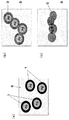
図6を参照しながら、導通経路の形態について更に説明する。図6は加熱硬化過程の前後における導電性接着剤の成分の状態を模式的に示している。尚、図6は各成分の状態を説明することを意図した図であるので、Agフィラー粒子の形状を便宜的に円形形状にしており、その形状が図2に示す形状と異なることに関して特に意味はない。図6(a)は、加熱前の状態を示しており、樹脂成分8の中に、低融点金属成分7の被覆を有するAgフィラー粒子が分散されて存在している。
The form of the conduction path will be further described with reference to FIG. FIG. 6 schematically shows the state of the components of the conductive adhesive before and after the heat curing process. 6 is a diagram intended to explain the state of each component. Therefore, the shape of the Ag filler particles is circular for convenience, and it is particularly meaningful regarding the fact that the shape is different from the shape shown in FIG. There is no. FIG. 6A shows a state before heating, in which Ag filler particles having a coating of the low melting
図6(b)は、その導電性接着剤を加熱して第1の形態の導通経路を形成した状態を示している。即ち、Agフィラー粒子が核となり、その周囲を低融点金属−Ag合金(本明細書及び図面に関して、少なくとも部分的にAgとの合金化を生じて得られた低融点金属−Ag合金を「Ag合金」とも称する)が包囲したうえで、Ag合金が相互に合一化又は一体化している。従って、図6(b)に示す例では、すべてのAgフィラー粒子をAg合金が包囲し相互に連絡して、第1の導通経路を形成している。 FIG. 6B shows a state in which the conductive adhesive is heated to form a conduction path of the first form. That is, Ag filler particles serve as nuclei, and a low melting point metal-Ag alloy (the low melting point metal-Ag alloy obtained by at least partially alloying with Ag in this specification and drawings is referred to as “Ag”. In addition, the Ag alloys are united or integrated with each other. Accordingly, in the example shown in FIG. 6B, all Ag filler particles are surrounded by an Ag alloy and are in communication with each other to form a first conduction path.
図6(c)は、加熱によってAgフィラー粒子の全体が低融点金属成分と合金化して第2の形態の導通経路を形成した状態を示している。但し、図6(c)に示す状態は、合金化が最も極端に進行した状態であって、実際には、加熱条件や低融点金属成分及びAgの組成等の条件等の種々の条件に応じて、図6(b)の状態と図6(c)の状態との間のいずれかの状態の程度にて合金化が進行すると考えるのが妥当である。尚、低融点金属成分にはAgフィラーに対して良好なぬれ性を示すものを用いており、そのことも周囲を低融点金属成分によって包囲されていないAgフィラー粒子が実質的に残らないようにすることに寄与し得る。 FIG. 6C shows a state in which the Ag filler particles as a whole are alloyed with the low melting point metal component by heating to form a conduction path of the second form. However, the state shown in FIG. 6 (c) is a state in which alloying has proceeded to the most extreme, and actually depends on various conditions such as heating conditions, conditions such as the low melting point metal component and Ag composition. Thus, it is appropriate to consider that alloying proceeds at a degree of any state between the state of FIG. 6B and the state of FIG. 6C. In addition, the low melting point metal component is one that exhibits good wettability with respect to the Ag filler, and this also prevents the Ag filler particles that are not surrounded by the low melting point metal component from substantially remaining. Can contribute to.
その後樹脂成分が硬化すると、少なくとも部分的に低融点金属−Ag合金から形成される金属塊(インゴット)によって実質的に切れ目なく連絡された導通経路を得ることができる。このようにランド3と電極2との間に、Agフィラー粒子を核として又は完全に合金化させて、低融点金属−Ag合金の金属塊によって実質的に切れ目のない導通経路が形成されているので、本発明の導電性接着剤を用いることによって、バルク金属並みでかつ安定した体積抵抗率を提供することができる。
Thereafter, when the resin component is cured, it is possible to obtain a conduction path that is substantially seamlessly connected by a metal lump (ingot) formed at least partially from a low-melting-point metal-Ag alloy. In this way, between the
尚、本発明の導電性接着剤を用いて、電子回路基板の配線を形成する場合には、図3における電極2は存在しない。しかし、基板上に未硬化の導電性接着剤組成物を所定のパターンにて塗布して加熱硬化させることによって、Agフィラー粒子を核として又は完全に合金化させて、実質的に切れ目のない低融点金属成分とAgとの合金の金属塊によって導通経路を形成することができるので、図3に示す例と同様に、実質的に切れ目のない金属塊の配線パターンを基板上に形成することができる。従って、この場合にも、本発明の導電性接着剤を用いることによって、バルク金属並みでかつ安定した体積抵抗率を達成することができる。従って、Cu等のバルク金属によって配線を形成した場合と同等の低い配線抵抗を得ることもできる。
In addition, when forming the wiring of an electronic circuit board using the conductive adhesive of this invention, the
更に、この低融点金属成分の合金は、鉛フリーはんだ材料やSn−Pb系はんだ材料よりも低い融点を示すので、より低い実装温度を達成することができる。 Furthermore, since this low melting point metal component alloy has a lower melting point than lead-free solder materials and Sn—Pb solder materials, a lower mounting temperature can be achieved.
この出願は、第3の発明として、樹脂成分が、第1の成分として硬化性樹脂を含み、第2の成分として還元性を有する樹脂を含むことを特長とする導電性接着剤を提供する。尚、導電性接着剤組成物としては、樹脂成分が還元性を有する樹脂のみを含む態様も含むことができる。硬化性樹脂及び金属フィラー成分については上述した第1及び第2の発明と同様のものを用いることができる。 This application provides, as a third invention, a conductive adhesive characterized in that the resin component includes a curable resin as the first component and a resin having a reducing property as the second component. In addition, as a conductive adhesive composition, the aspect in which a resin component contains only resin which has a reducing property can also be included. As for the curable resin and the metal filler component, those similar to those of the first and second inventions described above can be used.
例えば、従来の導電性接着剤を用いて電子部品を実装する場合に、加熱硬化過程において金属フィラー成分の粒子(金属フィラー粒子)が加熱されると、場合によって、金属フィラー粒子が溶融するよりも先に、金属フィラー粒子表面が酸化されてしまい、その結果、金属フィラー粒子の表面に酸化膜が形成されることがある。金属フィラー粒子の表面に生じた酸化膜は、金属フィラー粒子の溶融を妨害する1種の保護膜となって、導電性接着剤の加熱硬化過程における所定の温度で金属フィラー成分が溶融することを妨害したり、金属フィラー粒子どうしの接触部における電気抵抗を増大させたりして、導電性接着剤の機能を妨害し得る。その結果、加熱硬化過程を経た後に、十分に溶融し得なかった金属フィラー粒子が残ったり、体積抵抗率を上昇させたりし得る。 For example, when mounting an electronic component using a conventional conductive adhesive, if the metal filler component particles (metal filler particles) are heated in the heat curing process, the metal filler particles may be melted in some cases. First, the surface of the metal filler particles is oxidized, and as a result, an oxide film may be formed on the surface of the metal filler particles. The oxide film generated on the surface of the metal filler particles becomes a kind of protective film that hinders the melting of the metal filler particles, and the metal filler component melts at a predetermined temperature in the heat curing process of the conductive adhesive. The function of the conductive adhesive can be hindered by obstructing or increasing the electric resistance at the contact portion between the metal filler particles. As a result, after the heat curing process, metal filler particles that could not be sufficiently melted may remain, or the volume resistivity may be increased.
このような場合に、本発明の導電性接着剤を用いると、導電性接着剤中に還元性のある樹脂成分が存在しているので、加熱硬化過程中でも導電性接着剤組成物内をある程度還元性雰囲気に保つことができる。そのため、加熱硬化過程において金属フィラー粒子の表面に酸化膜が生じることを実質的に防止することができる。加熱硬化過程中における金属フィラー粒子表面の酸化を防止することによって、加熱硬化過程における低融点金属成分の溶融不良や、Agフィラー粒子表面に酸化膜が生成することを防止することができる。 In such a case, when the conductive adhesive of the present invention is used, a reducing resin component is present in the conductive adhesive, so that the inside of the conductive adhesive composition is reduced to some extent even during the heat curing process. A sex atmosphere can be maintained. Therefore, it is possible to substantially prevent the formation of an oxide film on the surface of the metal filler particles during the heat curing process. By preventing oxidation of the surface of the metal filler particles during the heat curing process, it is possible to prevent poor melting of the low melting point metal component during the heat curing process and the formation of an oxide film on the surface of the Ag filler particles.
1つの形態において、還元性のある樹脂はカルボキシル基を有する化合物、例えばカルボン酸を含むことが好ましい。樹脂中にそのような化合物を加えることによって、低融点金属の酸化膜を除去し(低融点金属の表面に酸化膜が生成することを防止し)、溶融し易くするため還元剤としての作用を発現させることができる。尚、そのような化合物には、脂肪族カルボン酸、芳香族カルボン酸、脂環式カルボン酸等の種々のカルボン酸を用いることができる。そのような化合物の例として、アジピン酸、アビチエン酸、アスコルビン酸、アクリル酸、クエン酸、ポリアクリル酸、リンゴ酸、ピメリン酸、パルミチン酸、ミリスチン酸、ラウリン酸、セバシン酸、スベリン酸、マレイン酸、コハク酸、アゼライン酸、フマル酸、グルタル酸、マロン酸等を挙げることができる。また、そのカルボン酸は、Na、Ag、Cu、K等の金属塩の形態であることが好ましい。 In one embodiment, the reducing resin preferably contains a compound having a carboxyl group, such as a carboxylic acid. By adding such a compound to the resin, the oxide film of the low melting point metal is removed (preventing the formation of an oxide film on the surface of the low melting point metal) and acts as a reducing agent to facilitate melting. Can be expressed. In addition, various carboxylic acids, such as aliphatic carboxylic acid, aromatic carboxylic acid, alicyclic carboxylic acid, can be used for such a compound. Examples of such compounds are adipic acid, abithienic acid, ascorbic acid, acrylic acid, citric acid, polyacrylic acid, malic acid, pimelic acid, palmitic acid, myristic acid, lauric acid, sebacic acid, suberic acid, maleic acid Succinic acid, azelaic acid, fumaric acid, glutaric acid, malonic acid and the like. The carboxylic acid is preferably in the form of a metal salt such as Na, Ag, Cu, or K.
もう1つの形態において、第2の樹脂成分として、金属を含む有機化合物を含有することが好ましい。常温では、金属は遊離することなく安定に有機化合物と化合又は結合しているが、加熱されると金属が有機化合物から遊離又は遊離過程となり、遊離した金属が樹脂の硬化反応を促進するようになる。その結果、短時間硬化及び保存安定性を両立させる硬化剤としての作用を果たすことができる。尚、そのような金属は、Na、Ag、Cu及びKの群の少なくとも1種であることが好ましい。 In another form, it is preferable to contain the organic compound containing a metal as a 2nd resin component. At normal temperature, the metal is stably combined with or bonded to the organic compound without being liberated, but when heated, the metal is liberated or liberated from the organic compound, and the liberated metal promotes the curing reaction of the resin. Become. As a result, it can serve as a curing agent that achieves both short-time curing and storage stability. In addition, it is preferable that such a metal is at least 1 sort (s) of the group of Na, Ag, Cu, and K.
もう1つの形態において、金属を含む有機化合物がカルボキシル基やアミノ基を含むことが好ましい。この場合には、カルボキシル基やアミノ基に由来する還元剤としての作用と、金属を含む有機化合物に由来する硬化剤としての作用とが、加熱硬化過程において相乗的に発揮され、良好な還元剤として作用させることができる。 In another embodiment, the organic compound containing a metal preferably contains a carboxyl group or an amino group. In this case, the action as a reducing agent derived from a carboxyl group or an amino group and the action as a curing agent derived from a metal-containing organic compound are synergistically exhibited in the heat curing process, and thus a good reducing agent. Can act as
第3の発明に関して、導電性接着剤組成物全体の重量に対する金属フィラー成分の重量の割合は、第1の発明の場合と同様であってよい。樹脂成分中において、第1の樹脂成分と第2の樹脂成分との割合は、重量基準で、90:10〜10:90の範囲、特に50:50〜80:20の範囲が好ましい。また、金属フィラー成分に対する第2の樹脂成分の割合は、20重量%以下が好適である。20重量%を超えると、還元剤及び/又は硬化剤としての作用にそれ以上の変化は認められないためである。尚、上記の第3の発明の効果が認められるためには、樹脂成分の割合は10重量%以上であることが好ましい。尚、第2の樹脂成分が硬化剤として作用する場合には、第1の樹脂成分に用いる硬化剤の使用量を減らすこともできる。 Regarding the third invention, the ratio of the weight of the metal filler component to the total weight of the conductive adhesive composition may be the same as in the first invention. In the resin component, the ratio of the first resin component and the second resin component is preferably in the range of 90:10 to 10:90, particularly in the range of 50:50 to 80:20, based on weight. Further, the ratio of the second resin component to the metal filler component is preferably 20% by weight or less. This is because when it exceeds 20% by weight, no further change is observed in the action as a reducing agent and / or a curing agent. In addition, in order to recognize the effect of said 3rd invention, it is preferable that the ratio of a resin component is 10 weight% or more. In addition, when the 2nd resin component acts as a hardening | curing agent, the usage-amount of the hardening | curing agent used for a 1st resin component can also be reduced.
また、この出願は、第4の発明として、第2又は第3の発明に係る導電性接着剤を用い、加熱する工程を行って所望する電気回路を形成する方法を提供する。従って、第2又は第3の発明に係る導電性接着剤を用いて基板に配線を形成し及び/又は電子部品を基板等へ接続することによって、電気回路を形成することができる。尚、この出願の第2の発明の導電性接着剤を用いることによって、170℃以下、好ましくは160℃以下、特に150℃以下の実装温度で電気回路を形成した後の導電性接着剤は、Ag合金化していることによって、適用した実装温度と同等又はそれを超える耐熱温度を具備することができる。 In addition, as a fourth invention, this application provides a method for forming a desired electric circuit by performing a heating step using the conductive adhesive according to the second or third invention. Therefore, an electric circuit can be formed by forming a wiring on a substrate and / or connecting an electronic component to the substrate or the like using the conductive adhesive according to the second or third invention. By using the conductive adhesive of the second invention of this application, the conductive adhesive after forming an electric circuit at a mounting temperature of 170 ° C. or lower, preferably 160 ° C. or lower, particularly 150 ° C. or lower, By forming an Ag alloy, it is possible to have a heat resistance temperature equal to or exceeding the applied mounting temperature.
更に、この出願は、第5の発明として、上述した電気回路を有する電気製品を提供する。得られる電気製品は、第2又は第3の発明に係る導電性接着剤によって、基板に配線が形成され及び/又は基板等に電子部品が接続された電気回路を有している。その電気回路は、第2又は第3の発明に関して本明細書に記載する特徴及び作用効果を有している。従って、この出願の第4の発明の電気回路を具備する電気製品には、実装温度と同等又はそれを超える温度環境であっても使用することができるものも含まれる。 Furthermore, this application provides an electric product having the above-described electric circuit as a fifth invention. The obtained electric product has an electric circuit in which wiring is formed on the substrate and / or electronic components are connected to the substrate or the like by the conductive adhesive according to the second or third invention. The electrical circuit has the features and advantages described herein with respect to the second or third invention. Therefore, the electric product including the electric circuit according to the fourth aspect of the present application includes one that can be used even in a temperature environment equal to or exceeding the mounting temperature.
本発明の金属フィラーは、導電性接着剤の金属フィラー成分として用いると、Agフィラーの周囲にて溶融した低融点金属成分がAgフィラー粒子と合金化して核となるAgフィラー粒子を包囲して又はAgを完全に合金化させて、隣接するAg合金どうしが合一化又は一体化して延びる導通経路を形成し、従って低融点金属−Ag合金を含む金属塊又は低融点金属−Ag合金の金属塊が実質的に切れ目なく連絡しているので、バルク金属並みでかつ安定した体積抵抗率を示す導通経路を形成することができる。 When the metal filler of the present invention is used as the metal filler component of the conductive adhesive, the low melting point metal component melted around the Ag filler surrounds the Ag filler particles which are alloyed with the Ag filler particles or Ag is completely alloyed to form a conduction path in which adjacent Ag alloys are united or integrated to extend, and thus a metal block including a low melting point metal-Ag alloy or a metal block of a low melting point metal-Ag alloy Are in contact with each other substantially without interruption, so that a conduction path having a volume resistivity equivalent to that of a bulk metal can be formed.
金属フィラー成分として、低融点金属成分によって表面が被覆されているAgフィラーを用いることによって、導電性接着剤を調製する操作に要する装置及び工程数、手間を簡略化することもできる。 By using an Ag filler whose surface is coated with a low-melting-point metal component as the metal filler component, it is possible to simplify the apparatus, the number of steps and labor required for the operation for preparing the conductive adhesive.
本発明の導電性接着剤は、金属フィラー成分の一部として比較的低融点の合金を用いるので、鉛フリーはんだ材料やSn−Pb系はんだ材料よりも低い硬化温度(または実装温度)を達成することができる。 Since the conductive adhesive of the present invention uses an alloy having a relatively low melting point as a part of the metal filler component, it achieves a lower curing temperature (or mounting temperature) than lead-free solder materials and Sn-Pb solder materials. be able to.
本発明の金属フィラーを金属フィラー成分中に含む導電性接着剤は、金属フィラーに関して上述した効果、即ち、Agフィラーの周囲にて溶融した低融点金属成分がAgフィラー粒子と合金化して核となるAgフィラー粒子を包囲して又はAgを完全に合金化させて、隣接するAg合金どうしが合一化又は一体化して延びる導通経路を形成し、従って低融点金属−Ag合金を含む金属塊又は低融点金属−Ag合金の金属塊が実質的に切れ目なく連絡しているので、バルク金属並みでかつ安定した体積抵抗率を示す導通経路を形成することができるという効果を奏することができる。 The conductive adhesive containing the metal filler of the present invention in the metal filler component has the effect described above with respect to the metal filler, that is, the low melting point metal component melted around the Ag filler is alloyed with the Ag filler particles and becomes a nucleus. Surrounding the Ag filler particles or completely alloying the Ag to form a conduction path in which adjacent Ag alloys are united or integrated to extend, and thus a metal mass containing low melting point metal-Ag alloy or low Since the metal lump of the melting point metal-Ag alloy communicates substantially seamlessly, it is possible to achieve an effect that a conduction path that is equivalent to a bulk metal and exhibits a stable volume resistivity can be formed.
本発明の導電性接着剤は、導電性接着剤中に還元性のある樹脂または硬化剤成分(第2の樹脂成分)を配合することにより、加熱硬化過程で低融点金属が酸化されることによる溶融不良を防止することができる。更に、第2の樹脂成分を加えることによって、低融点の合金をその融点にて十分に溶融させることができるので、この導電性接着剤は比較的低い実装温度で使用することができる。 The conductive adhesive of the present invention includes a reducing resin or a curing agent component (second resin component) contained in the conductive adhesive, whereby the low melting point metal is oxidized during the heat curing process. Melting defects can be prevented. Furthermore, since the low melting point alloy can be sufficiently melted at the melting point by adding the second resin component, the conductive adhesive can be used at a relatively low mounting temperature.
(第1の実施形態)
本発明の第1の形態において、表2に示すように、実施例1〜10としてそれぞれ対応する組成を有する低融点金属成分を配合して、得られる配合物(従って、対応する組成の合金)の融点及び体積抵抗率を測定した。
融点は、示差熱分析装置を用いて測定した。
体積抵抗率(ρ)の測定値は、試料について抵抗値R、配線長L及び断面積Sを求めた後、式:[ρ=R・L/S]に基づいて求めた。
(First embodiment)
In the first embodiment of the present invention, as shown in Table 2, the compounds obtained by blending low melting point metal components having compositions corresponding to Examples 1 to 10, respectively (and thus alloys having corresponding compositions). Were measured for melting point and volume resistivity.
The melting point was measured using a differential thermal analyzer.
The measured value of the volume resistivity (ρ) was obtained based on the equation: [ρ = R · L / S] after obtaining the resistance value R, the wiring length L, and the cross-sectional area S for the sample.
また、上記の各実施例に対応する組成の低融点金属成分とAgフィラー成分とを配合した金属フィラー成分を用いて、導電性接着剤を作製した。いずれの実施例についても、樹脂として、熱硬化性エポキシ樹脂を使用した。本発明に用いるのに好ましいエポキシ樹脂として、例えば、エピコート828、エピコート807(ジャパンエポキシレジン(JER)製)を、硬化剤として2PHZ(四国化成製)を挙げることができる。以下の例ではエピコート828を用いた。この樹脂成分15重量%に金属フィラー成分85重量%を配合して、導電性接着剤組成物を調製した。 Moreover, the conductive adhesive was produced using the metal filler component which mix | blended the low melting metal component and Ag filler component of the composition corresponding to said each Example. In all examples, a thermosetting epoxy resin was used as the resin. As preferred epoxy resins for use in the present invention, for example, Epicoat 828 and Epicoat 807 (manufactured by Japan Epoxy Resin (JER)) and 2PHZ (manufactured by Shikoku Kasei) can be cited as the curing agent. In the following example, Epicoat 828 was used. A conductive adhesive composition was prepared by blending 85% by weight of the metal filler component with 15% by weight of the resin component.
(Agに対するぬれ性の測定)
各実施例の低融点金属成分の組成に対応する合金について、Agに対するぬれ性を測定した。ぬれ性の評価は、以下のようにして求めた。図5に示すように、Agの薄い母材を用意してこれを加熱し、低融点金属成分合金の所定量をその母材上に載せた。低融点金属成分合金を溶融させて広がらせ、広がった低融点金属成分合金の最大高さhと、低融点金属成分合金がその量に対応する球の形態であると想定した場合の直径Dとを求め、式:[S=(D−h)/D]に基づいてぬれ広がり率(S)を求めた。
(Measurement of wettability to Ag)
The wettability with respect to Ag was measured about the alloy corresponding to the composition of the low melting-point metal component of each Example. The wettability was evaluated as follows. As shown in FIG. 5, a thin Ag base material was prepared and heated, and a predetermined amount of a low melting point metal component alloy was placed on the base material. The low melting point metal component alloy is melted and spread, the maximum height h of the spread low melting point metal component alloy, and the diameter D when the low melting point metal component alloy is assumed to be in the form of a sphere corresponding to the amount, And the wetting spread rate (S) was determined based on the formula: [S = (D−h) / D].
(導電性接着剤の体積抵抗率の測定)
各実施例に対応する導電性接着剤組成物を直方体の型の中に入れ、その型を温度150℃に保たれた加熱チャンバー内で5分間加熱して、導電性接着剤組成物を硬化させた。その後、室温まで放冷して、体積抵抗率を測定した。
(Measurement of volume resistivity of conductive adhesive)
The conductive adhesive composition corresponding to each example is placed in a rectangular parallelepiped mold, and the mold is heated in a heating chamber maintained at a temperature of 150 ° C. for 5 minutes to cure the conductive adhesive composition. It was. Then, it stood to cool to room temperature and measured the volume resistivity.
(繰り返し曲げ強度の測定)
また、繰り返し曲げ強度は、以下のようにして測定した。図4左図に示すように、相互に対応する接点を有する2枚のフレキ基板(厚さ0.08mm、長さ30mm、幅20mm)を用意し、フレキ基板の重ね代(接合部の長さ)を5mmとして、一方のフレキ基板の接点部分に本発明の導電性接着剤組成物を適量で塗布した。それから、対応する接点どうしを対向させて重ね合わせた後、上記の導電性接着剤の体積抵抗率の測定で行った加熱硬化過程に従って加熱処理を行い、導電性接着剤を十分に硬化させて、2枚のフレキ基板の接合を行った。
(Measurement of repeated bending strength)
The repeated bending strength was measured as follows. As shown in the left figure of FIG. 4, two flexible substrates (thickness 0.08 mm, length 30 mm, width 20 mm) having contact points corresponding to each other are prepared, and the overlapping amount of the flexible substrates (the length of the joining portion) ) Was 5 mm, and an appropriate amount of the conductive adhesive composition of the present invention was applied to the contact portion of one flexible substrate. Then, after overlapping the corresponding contacts facing each other, heat treatment according to the heat curing process performed in the measurement of the volume resistivity of the conductive adhesive, to sufficiently cure the conductive adhesive, Two flexible substrates were joined.
2枚のフレキ基板の接合部の上にR(半径)=1.0mmのステンレス棒を置いて、接合部を上方から押さえて固定した後、図4左図に示すように、上側の基板を、下側の基板の端部を延長した方向に延びる水平な姿勢から、その棒で押さえた部分を支点としてほぼ垂直上向きの姿勢(図4右図)へ曲げた後、再度水平な姿勢へ戻すという曲げ延ばしを繰り返した。曲げて延ばす1往復の動作を1回とカウントした。接合部に破断が生じるまで曲げ延ばしを繰り返し、破断が認められるに至るまでの回数を表1に示している。 After placing a stainless steel rod of R (radius) = 1.0 mm on the joint part of the two flexible boards and pressing the joint part from above to fix it, as shown in the left figure of FIG. Then, from a horizontal posture extending in the direction in which the end portion of the lower substrate is extended, the portion pressed by the rod is bent to a substantially vertical upward posture (right diagram in FIG. 4), and then returned to the horizontal posture again. The bending extension was repeated. One reciprocal motion of bending and extending was counted as one time. Table 1 shows the number of times until bending is repeated until breakage occurs in the joint and the breakage is recognized.
表1から判るように、SnにBi及び/又はInを添加することにより、導電性接着剤の体積抵抗率はAgのみを用いた比較例よりも比較的大きく低下し、はんだ合金並となっている。Agに対する相溶性の指標であるAgに対するぬれ性は、BiとInを複合添加することによってより向上している。また、Cu、Agを添加することにより、繰り返し曲げ強度はより向上している。Niを添加することにより溶融温度はやや低下し、機械的強度もより向上している。 As can be seen from Table 1, by adding Bi and / or In to Sn, the volume resistivity of the conductive adhesive is relatively lower than that of the comparative example using only Ag, which is comparable to that of the solder alloy. Yes. The wettability with respect to Ag, which is an index of compatibility with Ag, is further improved by adding Bi and In together. Moreover, repeated bending strength is further improved by adding Cu and Ag. By adding Ni, the melting temperature is slightly lowered and the mechanical strength is also improved.
(表1)フィラー組成と導電性接着剤特性(フィラー:樹脂=85wt%:15wt%)

(表2)金属組成と金属物性
(第2の実施形態)
本発明の第2の形態では、上記実施例1で用いた組成に、表3において実施例11〜15として示す還元性を有する第2の樹脂成分を更に配合して導電性接着剤組成物を調製した。樹脂成分と金属フィラー成分との重量比を15:85とし、樹脂成分中での第1の樹脂成分と第2の樹脂成分との重量比は50:50とした。
(Second Embodiment)
In the second mode of the present invention, the conductive adhesive composition is obtained by further blending the composition used in Example 1 with a second resin component having reducing properties shown as Examples 11 to 15 in Table 3. Prepared. The weight ratio of the resin component to the metal filler component was 15:85, and the weight ratio of the first resin component to the second resin component in the resin component was 50:50.
第2の成分の還元性を有する樹脂として、アジピン酸、アビチエン酸、アスコルビン酸、アクリル酸、クエン酸、ポリアクリル酸等を用いると、Snを含む合金フィラーの溶融性が向上し、体積抵抗率が低下することが確認された。また、硬化後のフィラーを観察すると、Sn含有フィラーが十分に溶融し、金属的な結合が得られていることが確認できた。 When adipic acid, abithienic acid, ascorbic acid, acrylic acid, citric acid, polyacrylic acid or the like is used as the resin having the reducing property of the second component, the meltability of the alloy filler containing Sn is improved and the volume resistivity is increased. Was confirmed to decrease. Further, when the cured filler was observed, it was confirmed that the Sn-containing filler was sufficiently melted and a metallic bond was obtained.
本発明の導電性接着剤は、電子部品の接合の用途及び配線形成の用途に有用である。
本発明の導電性接着剤は、硬化温度が鉛フリーはんだの融点よりも比較的低い温度にて実装に用いることができ、硬化後において、バルク金属並みでかつ安定した体積抵抗率を示すことができるので、許容耐熱温度が比較的低い電子部品の実装を、熱損傷を与える可能性を最小限度に小さくして、又は実質的に防止して、行う用途に特に有用である。
The conductive adhesive of the present invention is useful for joining electronic parts and wiring.
The conductive adhesive of the present invention can be used for mounting at a curing temperature that is relatively lower than the melting point of lead-free solder, and exhibits a volume resistivity equivalent to that of a bulk metal after curing. As such, it is particularly useful in applications where the mounting of electronic components with a relatively low allowable temperature limit is done with minimal or substantially no potential for thermal damage.
また、本発明の導電性接着剤は、CCD素子、フォログラム素子、チップ部品等の電子部品の接続用及びそれらを接合する基板の配線形成に用いることができる。その結果、これらの素子、部品及び/又は基板を内蔵する製品、例えば、DVD、携帯電話、ポータブルAV機器、ノートPC、デジタルカメラ等に使用することができる。 In addition, the conductive adhesive of the present invention can be used for connecting electronic components such as CCD elements, holographic elements, and chip parts, and for forming a wiring on a substrate for joining them. As a result, it can be used for products incorporating these elements, components and / or substrates, for example, DVDs, mobile phones, portable AV devices, notebook PCs, digital cameras and the like.
1:Sn−Pb系はんだ、 2:部品電極、 3:電子回路基板のランド、
4:CuSn化合物層、 5:Agフィラー、 6:溶融及び固化した金属フィラー、
7:Agフィラーを被覆している低融点金属成分、 8:導電性接着剤の樹脂成分、
9:Ag合金。
1: Sn—Pb solder, 2: Component electrode, 3: Land of electronic circuit board,
4: CuSn compound layer, 5: Ag filler, 6: Molten and solidified metal filler,
7: low melting point metal component covering Ag filler, 8: resin component of conductive adhesive,
9: Ag alloy.
Claims (5)
Priority Applications (1)
| Application Number | Priority Date | Filing Date | Title |
|---|---|---|---|
| JP2006067582A JP4975342B2 (en) | 2005-03-15 | 2006-03-13 | Conductive adhesive |
Applications Claiming Priority (3)
| Application Number | Priority Date | Filing Date | Title |
|---|---|---|---|
| JP2005072597 | 2005-03-15 | ||
| JP2005072597 | 2005-03-15 | ||
| JP2006067582A JP4975342B2 (en) | 2005-03-15 | 2006-03-13 | Conductive adhesive |
Publications (3)
| Publication Number | Publication Date |
|---|---|
| JP2006294600A JP2006294600A (en) | 2006-10-26 |
| JP2006294600A5 JP2006294600A5 (en) | 2009-04-23 |
| JP4975342B2 true JP4975342B2 (en) | 2012-07-11 |
Family
ID=37414906
Family Applications (1)
| Application Number | Title | Priority Date | Filing Date |
|---|---|---|---|
| JP2006067582A Expired - Fee Related JP4975342B2 (en) | 2005-03-15 | 2006-03-13 | Conductive adhesive |
Country Status (1)
| Country | Link |
|---|---|
| JP (1) | JP4975342B2 (en) |
Families Citing this family (8)
| Publication number | Priority date | Publication date | Assignee | Title |
|---|---|---|---|---|
| JP4897697B2 (en) * | 2005-11-02 | 2012-03-14 | パナソニック株式会社 | Conductive adhesive |
| US7910837B2 (en) * | 2007-08-10 | 2011-03-22 | Napra Co., Ltd. | Circuit board, electronic device and method for manufacturing the same |
| JP5380810B2 (en) * | 2007-09-28 | 2014-01-08 | 三洋電機株式会社 | Solar cell module |
| KR101011199B1 (en) * | 2007-11-01 | 2011-01-26 | 파나소닉 주식회사 | Mounting structure |
| WO2013039213A1 (en) * | 2011-09-15 | 2013-03-21 | 凸版印刷株式会社 | Structure for connecting electroconductive members, metal foil pattern laminate, and solar cell module |
| JP6397742B2 (en) * | 2013-12-03 | 2018-09-26 | 積水化学工業株式会社 | Conductive particles, conductive materials, and connection structures |
| JP6474008B2 (en) * | 2017-03-29 | 2019-02-27 | パナソニックIpマネジメント株式会社 | Connecting material |
| WO2024058254A1 (en) * | 2022-09-16 | 2024-03-21 | 日亜化学工業株式会社 | Ceramic sintered body substrate, light-emitting device, and methods for manufacturing these |
Family Cites Families (7)
| Publication number | Priority date | Publication date | Assignee | Title |
|---|---|---|---|---|
| JPH07179832A (en) * | 1993-12-24 | 1995-07-18 | Toyota Motor Corp | Conductive adhesive |
| JP3347512B2 (en) * | 1995-03-17 | 2002-11-20 | 富士通株式会社 | Solder alloy for low-temperature bonding, electronic device using the same, and method of manufacturing the same |
| JPH1025461A (en) * | 1996-05-10 | 1998-01-27 | Sekisui Chem Co Ltd | Acrylic pressure-sensitive adhesive composition |
| JPH11317487A (en) * | 1998-05-01 | 1999-11-16 | Nissan Motor Co Ltd | Electronic device and mounting method therefor |
| JP3386009B2 (en) * | 1998-07-01 | 2003-03-10 | 富士電機株式会社 | Solder alloy |
| JP4359983B2 (en) * | 1999-12-24 | 2009-11-11 | 株式会社豊田中央研究所 | Electronic component mounting structure and manufacturing method thereof |
| JP4244736B2 (en) * | 2003-07-02 | 2009-03-25 | 旭硝子株式会社 | Conductive adhesive, its bonding method, and automotive window glass using the same |
-
2006
- 2006-03-13 JP JP2006067582A patent/JP4975342B2/en not_active Expired - Fee Related
Also Published As
| Publication number | Publication date |
|---|---|
| JP2006294600A (en) | 2006-10-26 |
Similar Documents
| Publication | Publication Date | Title |
|---|---|---|
| JP5090349B2 (en) | Bonding material, bonding part and circuit board | |
| JP4975342B2 (en) | Conductive adhesive | |
| JP5238088B1 (en) | Solder alloy, solder paste and electronic circuit board | |
| KR101538293B1 (en) | Solder alloy, solder paste, and electronic circuit board | |
| KR102566561B1 (en) | Solder alloys, solder pastes and electronic circuit boards | |
| JP5722302B2 (en) | Lead-free solder alloy, solder paste using this, and mounted product | |
| JP2014028391A (en) | Solder alloy, solder paste, and electronic circuit substrate | |
| JP4897697B2 (en) | Conductive adhesive | |
| WO2013132942A1 (en) | Bonding method, bond structure, and manufacturing method for same | |
| KR20190122741A (en) | Solder Materials, Solder Pastes, Foam Solders and Solder Joints | |
| JPWO2017018167A1 (en) | Solder alloy, solder paste and electronic circuit board | |
| JP3886144B1 (en) | Bonding materials, electronic components and bonding structures | |
| JP4939072B2 (en) | Conductive adhesive | |
| US20210354251A1 (en) | Resin flux solder paste and mount structure | |
| KR102342394B1 (en) | Solder Alloy, Solder Paste, Preform Solder, Solder Ball, Wire Solder, Resin Flux Cored Solder, Solder Joint, Electronic Circuit Board and Multilayer Electronic Circuit Board | |
| JP3782743B2 (en) | Solder composition, soldering method and electronic component | |
| KR20150111403A (en) | A Pb FREE SOLDERING FLUX AND PASTE FOR ELECTRONIC COMPONENT, AND A SOLDERING METHOD USING THE SAME MATERIALS | |
| JP5699472B2 (en) | Solder material, manufacturing method thereof, and manufacturing method of semiconductor device using the same | |
| JP2016087691A (en) | Pb-FREE SOLDER AND ELECTRONIC PARTS BUILT-IN MODULE | |
| JP2008221330A (en) | Solder alloy | |
| JP6417692B2 (en) | Solder composition, solder paste, solder joint structure, and electronic device | |
| JP5140328B2 (en) | CONDUCTIVE CONNECTION FORMED BY USING CONDUCTIVE ADHESIVE AND CIRCUIT BOARD AND ELECTRONIC ELECTRIC DEVICE USING THE CONDUCTIVE CONNECTION | |
| JP4692491B2 (en) | Bonding material | |
| JP2019150880A (en) | Solder material, solder paste, foam solder, and solder joint | |
| JP2015136735A (en) | BALL-SHAPED Au-Sn-Ag TYPE SOLDER ALLOY, ELECTRONIC PART SEALED BY USING BALL-SHAPED Au-Sn-Ag TYPE SOLDER ALLOY AND ELECTRONIC PART MOUNTING DEVICE |
Legal Events
| Date | Code | Title | Description |
|---|---|---|---|
| A521 | Request for written amendment filed |
Free format text: JAPANESE INTERMEDIATE CODE: A523 Effective date: 20090306 |
|
| A621 | Written request for application examination |
Free format text: JAPANESE INTERMEDIATE CODE: A621 Effective date: 20090306 |
|
| A977 | Report on retrieval |
Free format text: JAPANESE INTERMEDIATE CODE: A971007 Effective date: 20101208 |
|
| A131 | Notification of reasons for refusal |
Free format text: JAPANESE INTERMEDIATE CODE: A131 Effective date: 20110104 |
|
| A521 | Request for written amendment filed |
Free format text: JAPANESE INTERMEDIATE CODE: A523 Effective date: 20110304 |
|
| A131 | Notification of reasons for refusal |
Free format text: JAPANESE INTERMEDIATE CODE: A131 Effective date: 20111227 |
|
| TRDD | Decision of grant or rejection written | ||
| A01 | Written decision to grant a patent or to grant a registration (utility model) |
Free format text: JAPANESE INTERMEDIATE CODE: A01 Effective date: 20120403 |
|
| A01 | Written decision to grant a patent or to grant a registration (utility model) |
Free format text: JAPANESE INTERMEDIATE CODE: A01 |
|
| A61 | First payment of annual fees (during grant procedure) |
Free format text: JAPANESE INTERMEDIATE CODE: A61 Effective date: 20120411 |
|
| R150 | Certificate of patent or registration of utility model |
Ref document number: 4975342 Country of ref document: JP Free format text: JAPANESE INTERMEDIATE CODE: R150 Free format text: JAPANESE INTERMEDIATE CODE: R150 |
|
| FPAY | Renewal fee payment (event date is renewal date of database) |
Free format text: PAYMENT UNTIL: 20150420 Year of fee payment: 3 |
|
| LAPS | Cancellation because of no payment of annual fees |