JP4969430B2 - Pressure detection device - Google Patents
Pressure detection device Download PDFInfo
- Publication number
- JP4969430B2 JP4969430B2 JP2007324161A JP2007324161A JP4969430B2 JP 4969430 B2 JP4969430 B2 JP 4969430B2 JP 2007324161 A JP2007324161 A JP 2007324161A JP 2007324161 A JP2007324161 A JP 2007324161A JP 4969430 B2 JP4969430 B2 JP 4969430B2
- Authority
- JP
- Japan
- Prior art keywords
- electronic component
- lead material
- lead
- pressure detection
- detection device
- Prior art date
- Legal status (The legal status is an assumption and is not a legal conclusion. Google has not performed a legal analysis and makes no representation as to the accuracy of the status listed.)
- Expired - Lifetime
Links
Images


Classifications
-
- H—ELECTRICITY
- H01—ELECTRIC ELEMENTS
- H01L—SEMICONDUCTOR DEVICES NOT COVERED BY CLASS H10
- H01L2924/00—Indexing scheme for arrangements or methods for connecting or disconnecting semiconductor or solid-state bodies as covered by H01L24/00
- H01L2924/0001—Technical content checked by a classifier
- H01L2924/0002—Not covered by any one of groups H01L24/00, H01L24/00 and H01L2224/00
Description
本発明は、圧力検出装置の他、空気流量検出装置,回転信号検出装置,角度検出装置,点火装置等の電子装置全般に係わり、詳しくは、リード材と一体成形された外装ケースに、出力信号を有する電子回路と、電気的外乱を低減する電子部品とを実装する構造に関するものである。 The present invention relates to general electronic devices such as an air flow rate detection device, a rotation signal detection device, an angle detection device, and an ignition device, in addition to a pressure detection device. Specifically, an output signal is output to an outer case integrally formed with a lead material. The present invention relates to a structure for mounting an electronic circuit having an electronic component and an electronic component that reduces electrical disturbance.
従来の技術は、特許文献1に記載のように、搭載する電子部品の位置決めを目的とした窪みを設け、位置ずれを防止する方法がとられていた。
In the conventional technique, as described in
その他の従来技術としては、電気的外乱を低減する電子部品として、リード線付きのコンデンサ等を用いていたが、形状が大きく小型化できない。リード線がアンテナとなり、電気的外乱を受けやすい等の問題があることから、小型のチップコンデンサ及びチップインダクタ等の小型素子を用いることが望ましい。 As another conventional technique, a capacitor with a lead wire or the like is used as an electronic component for reducing electrical disturbance, but the shape is large and cannot be reduced in size. It is desirable to use small elements such as small chip capacitors and chip inductors because the lead wire becomes an antenna and is susceptible to electrical disturbance.
上記従来技術は、搭載する電子部品の位置決め用の窪みであり、接続部材の厚みに対する考慮まではされておらず、接続部材の厚さがばらつく問題があった。 The prior art described above is a depression for positioning electronic components to be mounted, and the thickness of the connecting member is not taken into consideration, and there is a problem that the thickness of the connecting member varies.
実験によると、樹脂製の外装ケースに一体成形されたリード材間に電子部品を実装した場合、各材料の線膨張係数の差から発生した熱ストレスによって接続部材にクラックが発生,進行することが確認されている。クラックの進行速度は、接続部材の厚みと関連性を持っていることから、クラックに対する信頼性を確保するためには、接続部材の厚さの管理が重要となってくる。 According to experiments, when electronic components are mounted between lead materials that are integrally molded in a resin outer case, cracks may occur in the connecting member due to thermal stress generated by the difference in the linear expansion coefficient of each material. It has been confirmed. Since the progress speed of the crack is related to the thickness of the connecting member, it is important to manage the thickness of the connecting member in order to ensure reliability against the crack.
また、外装ケースに検出部を接続後、接続部材のひとつであるはんだを用いて電子部品を接続する場合、はんだの鉛フリー化等により、使用するはんだの融点が高くなる傾向にあるため、従来のリフロー方式が困難となってきている。更に、リフロー時の熱によって検出部にダメージを与える恐れがあるため、検出部及び外装ケースに熱的ダメージを与えない接続プロセスが必要となってくる。 In addition, when connecting an electronic component using solder, which is one of the connecting members, after connecting the detection unit to the exterior case, the melting point of the solder to be used tends to increase due to lead-free solder, etc. The reflow method has become difficult. Furthermore, since there is a risk of damage to the detection unit due to heat during reflow, a connection process that does not cause thermal damage to the detection unit and the outer case is necessary.
本発明の目的は、搭載する電子部品の位置ずれを防止しながら、接続部材の厚みを確保することで、接続部における熱ストレスから発生するクラックに対する信頼性を向上させることにある。 An object of the present invention is to improve the reliability with respect to cracks generated from thermal stress in a connection part by ensuring the thickness of the connection member while preventing the displacement of electronic components to be mounted.
更なる目的は、クラックに対する信頼性を向上させるとともに配線間の短絡を防止することにある。 A further object is to improve reliability against cracks and prevent short circuits between wirings.
上記目的は、圧力検出手段と、前記圧力検出手段が設置される樹脂ケースと、前記樹脂ケースに一体モールドされ、一方が外部との電気的接続用コネクタ端子となり、前記圧力検出手段からの信号を前記端子を介して出力するための複数のリード材とを備えた圧力検出装置において、前記樹脂ケースの開口部で、前記第1のリード材と前記第2のリード材とに接続部材により接続面が各々に接続された電子部品を備え、前記第1のリード材と前記第2のリード材の前記電子部品の接続面と対向する位置に、二段以上の異なった深さを有する窪みが互いのリード材に対となる様に設けられたことにより達成される。
The purpose is to provide a pressure detection means, a resin case in which the pressure detection means is installed, and a resin case integrally molded, one of which is a connector terminal for electrical connection to the outside, and a signal from the pressure detection means. In the pressure detection apparatus including a plurality of lead materials for outputting via the terminals, a connection surface is formed by a connection member between the first lead material and the second lead material at the opening of the resin case. There comprising electronic components connected to each, to the connection surface opposite to the position of the electronic component of the second lead member and said first lead member, the recess having a different depth of more than two stages to each other This is achieved by providing a pair with the lead material.
本発明によれば、クラックに対する信頼性を向上させるとともに配線間の短絡を防止することができる。 ADVANTAGE OF THE INVENTION According to this invention, the reliability with respect to a crack can be improved, and the short circuit between wiring can be prevented.
以下、図1,図2を用いて、本発明の一実施形態,構成について説明する。 Hereinafter, an embodiment and a configuration of the present invention will be described with reference to FIGS.
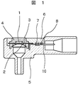
図1は圧力検出装置の縦断面図である。図2は圧力検出装置の正面図である。 FIG. 1 is a longitudinal sectional view of the pressure detection device. FIG. 2 is a front view of the pressure detection device.
検出部1はシリコンにダイアフラムと回路を形成し、ガラス台座と陽極接合して構成されている。
The
検出部ケース4は、エポキシ樹脂等の熱硬化性樹脂または、PPS樹脂等の熱可塑性樹脂から成り、検出部端子3はニッケルメッキを施したリン青銅で構成される。
The
検出部ケース4には前記検出部1が接着固定されている。また検出部ケース4にインサート成型された検出部端子3と前記検出部1とは、アルミまたは金から成る接続ワイヤ2で接続され、電気的接続がとられている。
The
外装ケース5は、PBTまたはPPSなどの樹脂材と金属製のリード材9,10,11で構成され、前記検出部ケース4及び電子部品7,8を実装するため開口しており、外側をコネクタの形状とし、外部に信号を出力する構造となっている。
The
前記外装ケース5の開口部に、前記検出部ケース4を搭載し、検出部端子3と各リード材9,10,11を溶接によって接続し、更に各リード材9,10,11間を跨ぐように電子部品7,8をはんだまたは導電性ペーストからなる接続部材14で電気的接続を確保させた後、外装ケースの開口部にエポキシまたはシリコーン樹脂等の封止材6を隙間無く注入硬化させて圧力検出装置が完成される。
The
図3〜図12において、本発明の特徴を説明する。 The features of the present invention will be described with reference to FIGS.
図3は図2中のリード材9,10,11のみを抽出した図である。
FIG. 3 is a diagram in which only the
リード材9,10,11には、電子部品7,8を搭載するための窪み12,13更にその内側に接続部材厚さ確保用の窪み16が形成されている。
In the
図4は図3のB部の窪み13に電子部品8を実装した状態での詳細正面図とその側面図である。
FIG. 4 is a detailed front view and a side view of the
リード材11上の電子部品8を搭載すべき位置に、電子部品8を包囲するように位置決め用の窪み13が形成され、その内側に電子部品8よりも狭い幅で、はんだまたは導電性ペーストからなる接続部材14の厚み確保用の窪み16が形成されている。この結果、電子部品8を搭載した場合、位置決め用窪み13によって位置ずれが防止されると共に、接続部材厚み確保用の窪み16によって、接続部材14の最低厚みを確保することが可能となる。
A
図5は、図4に対し、位置決め用窪み13の角部を残した形状で接続部材厚み確保用の窪み16を形成した例である。この場合、電子部品8の角部が位置決め用窪み13の底面によって支持されるため図4の実施例と同様の効果を得ることができる。
FIG. 5 shows an example in which the recess 16 for securing the thickness of the connecting member is formed in a shape that leaves the corners of the positioning recess 13 with respect to FIG. In this case, since the corners of the
図6は、図4に対し、接続部材厚み確保用の突起17を設けた例である。この場合、接続部材厚み確保用の突起17が電子部品8を支持するため図4の実施例と同様の効果を得ることができる。
FIG. 6 is an example in which a
前記接続部材厚み確保用の突起13は複数個形成しても良い。
A plurality of
図7は、図4に対し、位置決め用窪み13を接続部材14の必要厚みより深く形成し、さらに接続部材14に必要厚さ相当の大きさとなる導電性固形物15を混合して接続した例である。この場合、接続部材14に混合した導電性固形物15が、電子部品8を支持するため図4の実施例と同様の効果を得ることができる。
FIG. 7 shows an example in which the
図8は、図7に対し、搭載する電子部品8の接続面側に接続部材厚み確保用の窪み13をエッチング等により形成した例である。また、他の実施例同様、突起を形成しても効果が得られる。
FIG. 8 is an example in which a
図9は、従来技術の位置決め用窪み13のみを形成し、接続部材14を用いて電子部品8を接続した例である。この場合、接続部材14の厚さは、接続部材14が溶融硬化する際の表面張力によって決まってくるが、ばらつきが大きいため、作業条件のみで管理するのは困難であった。
FIG. 9 shows an example in which only the positioning recess 13 of the prior art is formed and the
図10は、本実施例において、接続部材14にはんだを用いた場合での、冷熱サイクル耐久試験後におけるはんだの厚さTとはんだに発生するクラック発生率の関係を実験より求め、示したグラフである。
FIG. 10 is a graph illustrating the relationship between the thickness T of the solder after the thermal cycle endurance test and the rate of occurrence of cracks generated in the solder when the solder is used for the
各構成材料の線膨張係数の差によって熱ストレスが発生し、繰り返されることによってはんだにクラックが発生,進行する。 Thermal stress is generated due to the difference in coefficient of linear expansion of each constituent material, and cracks are generated and progressed by being repeated.
実験の結果によると、はんだ厚さTが厚くなるほど耐久後のクラック発生率が少ない傾向にある。また電子部品長さLが長くなるほどはんだ厚さTが必要となってくる。本実施例の場合、電子部品7,8の長さが一番長い仕様において、耐久試験後のクラックを防止できるはんだ厚さは70μm以上必要となる。
According to the result of the experiment, the higher the solder thickness T, the smaller the crack generation rate after durability. Further, as the electronic component length L becomes longer, the solder thickness T becomes necessary. In the case of the present embodiment, in the specification in which the lengths of the
本実施例によると、接続部の信頼性を左右する接続部材14の厚みを管理することが可能となり、信頼性を確保できる効果がある。
According to the present embodiment, it is possible to manage the thickness of the
図11は、図2中のA−A断面図である。外装ケース5に一体成型されたリード材9,11上に接続部材14を用いてチップコンデンサからなる電子部品7が接続されている。これら構成部品を、線膨張係数が外装ケース5よりも小さくかつ電子部品7よりも大きな封止材6で隙間無くモールド封止することで、熱による変位を拘束し、接続部材14に発生するクラックの進行が抑制され、接続部の信頼性を確保できる効果がある。また、接続部材14にはんだを用いた場合、接続部材14の表面に析出したフラックスを溶かす性質の封止材6を用いることで、各部品と封止材6が接合し、熱による変位を拘束することが可能となる。更に隣接するそれぞれのリード材9,10,11との空間を封止材6で隙間無く封止することで、経時変化による接続部材14の変形及び成長による短絡を防止することが可能となる。
11 is a cross-sectional view taken along line AA in FIG. An
図12は、電子部品7を、接続部材14にはんだを用いて接続する工程における図2中のA−A断面図である。接続部材14であるはんだを接続する方法として、光18を照射している。図2におけるC部で示す範囲に限り光18を照射することで、外装ケース5及び検出部1に熱的ダメージを与えることなくはんだを溶かすことが可能となる。更に、光18を電子部品7,8を含む図2中C部の範囲に均一に照射することで、レーザー等のスポット照射時に発生する局所的な過加熱による電子部品7,8へのダメージを回避しながら、安定してはんだを接続することが可能となる。
FIG. 12 is a cross-sectional view taken along line AA in FIG. 2 in the process of connecting the
電子部品搭載部に位置決め用の窪みに加えて窪み又は突起等を設けることで、接続部材の厚さを管理することが可能となり、接続部の信頼性を確保できる効果がある。 By providing the electronic component mounting portion with a recess or protrusion in addition to the positioning recess, the thickness of the connection member can be managed, and the reliability of the connection portion can be ensured.
更に、封止材で電子部品搭載部を隙間無く封止,拘束することで、接続部材に発生するクラックの進行を抑制するとともに、接続部材の変形,成長によるリード材間の短絡を防止し、接続部の信頼性を確保できる効果がある。 Furthermore, by sealing and restraining the electronic component mounting portion with a sealing material without any gap, the progress of cracks occurring in the connection member is suppressed, and a short circuit between the lead materials due to deformation and growth of the connection member is prevented. There is an effect of ensuring the reliability of the connecting portion.
また、接続部材にはんだを用いた場合、光照射方式を用いることで、検出部及び外装ケースにダメージを与えることなく接続できる効果がある。 Further, when solder is used for the connection member, the light irradiation method can be used to connect the detection unit and the outer case without damaging them.
1…検出部、2…接続ワイヤ、3…検出部端子、4…検出部ケース、5…外装ケース、6…封止材、7,8…電子部品。
DESCRIPTION OF
Claims (9)
前記圧力検出手段が設置される樹脂ケースと、
前記樹脂ケースに一体モールドされ、一方が外部との電気的接続用コネクタ端子となり、前記圧力検出手段からの信号を前記端子を介して出力するための複数のリード材とを備えた圧力検出装置において、
前記樹脂ケースの開口部で、前記第1のリード材と前記第2のリード材とに接続部材により接続面が各々に接続された電子部品を備え、
前記第1のリード材と前記第2のリード材の前記電子部品の接続面と対向する位置に、二段以上の異なった深さを有する窪みが互いのリード材に対となる様に設けられたことを特徴とする圧力検出装置。 Pressure detection means;
A resin case in which the pressure detecting means is installed;
In a pressure detection device comprising a plurality of lead members for integrally molding the resin case, one of which serves as a connector terminal for electrical connection to the outside, and for outputting a signal from the pressure detection means via the terminal ,
In the opening of the resin case, the first lead material and the second lead material, each having a connection surface connected to each other by a connection member,
A position wherein the opposed and connecting surface of the electronic component of the second lead member and said first lead member, the recess having two or more stages of different depths are provided so as a pair to each other lead material A pressure detection device characterized by that.
前記圧力検出手段が、ダイアフラムと回路とを形成するシリコン、前記シリコンが固定された検出部ケース、前記検出部ケースにインサート成形された検出部端子と、前記検出部端子と前記回路とを電気的に接続する接続ワイヤとから形成され、
前記開口部で、前記検出部端子と前記リード材とが接続されたことを特徴とする圧力検出装置。 In claim 1,
The pressure detection means electrically connects the silicon forming the diaphragm and the circuit, the detection unit case to which the silicon is fixed, the detection unit terminal insert-molded in the detection unit case, and the detection unit terminal and the circuit. A connecting wire that connects to the
The pressure detection device, wherein the detection unit terminal and the lead material are connected to each other through the opening.
前記開口部を封止する封止部材を備えたことを特徴とする圧力検出装置。 In claim 1 or 2,
A pressure detection device comprising a sealing member for sealing the opening.
前記第1のリード材と前記第2のリード材との間に延在し、かつ、前記電子部品の下を横切り、前記電子部品に接続されない第3のリード材を備えたことを特徴とする圧力検出装置。 In claim 1,
A third lead material is provided that extends between the first lead material and the second lead material, crosses under the electronic component, and is not connected to the electronic component. Pressure detection device.
前記第1のリード材と前記第2のリード材とに設けられた前記窪みには、前記電子部品を包囲するように設けられた位置決め用窪みと、前記位置決め用窪みよりも内側に設けられた前記接続部材の厚み確保用窪みと、が形成されたことを特徴とする圧力検出装置。 In claim 1,
In the recesses provided in the first lead material and the second lead material, a positioning recess provided so as to surround the electronic component and an inner side than the positioning recess are provided. A pressure detecting device, wherein a recess for securing the thickness of the connecting member is formed.
前記第1のリード材と前記第2のリード材とに設けられた前記窪みには、前記電子部品を包囲するように設けられた位置決め用窪みと、底面に設けられた突起とが形成されたことを特徴とする圧力検出装置。 In claim 1,
A positioning recess provided to surround the electronic component and a protrusion provided on the bottom surface are formed in the recess provided in the first lead material and the second lead material. A pressure detection device characterized by that.
前記接続部材ははんだであって、
前記封止部材は、線膨張係数が前記樹脂ケースよりも小さく、かつ前記電子部品よりも大きく、かつ、前記はんだから析出したはんだフラックスを溶かす性質を持つ樹脂であることを特徴とする圧力検出装置。 In claim 3,
The connecting member is solder,
The pressure detecting device, wherein the sealing member is a resin having a linear expansion coefficient smaller than that of the resin case, larger than that of the electronic component, and having a property of melting a solder flux deposited from the solder. .
前記第1のリード材と前記電子部品との間、および、前記第2のリード材と前記電子部品との間の接続部材には、その厚みが70μm以上の部分が形成されたことを特徴とする圧力検出装置。 In claim 1,
The connection member between the first lead material and the electronic component and between the second lead material and the electronic component is formed with a portion having a thickness of 70 μm or more. Pressure detector.
前記接続部材ははんだであって、前記電子部品はチップコンデンサであることを特徴とする圧力検出装置。 In any one of Claim 1 to 8,
The pressure detecting device, wherein the connecting member is solder and the electronic component is a chip capacitor.
Priority Applications (1)
| Application Number | Priority Date | Filing Date | Title |
|---|---|---|---|
| JP2007324161A JP4969430B2 (en) | 2007-12-17 | 2007-12-17 | Pressure detection device |
Applications Claiming Priority (1)
| Application Number | Priority Date | Filing Date | Title |
|---|---|---|---|
| JP2007324161A JP4969430B2 (en) | 2007-12-17 | 2007-12-17 | Pressure detection device |
Related Parent Applications (1)
| Application Number | Title | Priority Date | Filing Date |
|---|---|---|---|
| JP2003154273A Division JP2004356494A (en) | 2003-05-30 | 2003-05-30 | Electronic equipment and pressure detection device |
Publications (3)
| Publication Number | Publication Date |
|---|---|
| JP2008151792A JP2008151792A (en) | 2008-07-03 |
| JP2008151792A5 JP2008151792A5 (en) | 2010-07-29 |
| JP4969430B2 true JP4969430B2 (en) | 2012-07-04 |
Family
ID=39654071
Family Applications (1)
| Application Number | Title | Priority Date | Filing Date |
|---|---|---|---|
| JP2007324161A Expired - Lifetime JP4969430B2 (en) | 2007-12-17 | 2007-12-17 | Pressure detection device |
Country Status (1)
| Country | Link |
|---|---|
| JP (1) | JP4969430B2 (en) |
Families Citing this family (4)
| Publication number | Priority date | Publication date | Assignee | Title |
|---|---|---|---|---|
| JP5712799B2 (en) * | 2011-06-03 | 2015-05-07 | 株式会社デンソー | Sensor and manufacturing method thereof |
| JP2014195039A (en) * | 2013-02-26 | 2014-10-09 | Tokai Rika Co Ltd | Connection structure of electronic component |
| EP3109897A1 (en) * | 2015-06-23 | 2016-12-28 | Nxp B.V. | A lead frame assembly |
| US9681568B1 (en) * | 2015-12-02 | 2017-06-13 | Ge Energy Power Conversion Technology Ltd | Compact stacked power modules for minimizing commutating inductance and methods for making the same |
Family Cites Families (8)
| Publication number | Priority date | Publication date | Assignee | Title |
|---|---|---|---|---|
| JPH01105565A (en) * | 1987-10-17 | 1989-04-24 | Matsushita Electric Ind Co Ltd | Lead frame for hybrid integrated circuit |
| JPH06268120A (en) * | 1993-03-16 | 1994-09-22 | Hitachi Ltd | Heat sink for power switching module |
| JP4117807B2 (en) * | 1997-06-24 | 2008-07-16 | 松下電工株式会社 | Electronic component soldering method |
| JP2000165042A (en) * | 1998-11-30 | 2000-06-16 | Nec Corp | Thin film multilayer wiring board |
| JP2002124616A (en) * | 2000-10-13 | 2002-04-26 | Aisan Ind Co Ltd | Chip-component mounting structure on lead frame |
| JP2002151612A (en) * | 2000-11-10 | 2002-05-24 | Sumitomo Metal Electronics Devices Inc | Package for optical communication and its manufacturing method |
| JP3791403B2 (en) * | 2000-12-04 | 2006-06-28 | 富士電機ホールディングス株式会社 | No-clean flux for lead-free solder and solder composition containing the same |
| JP3752444B2 (en) * | 2001-11-16 | 2006-03-08 | 株式会社日立製作所 | Pressure detection device |
-
2007
- 2007-12-17 JP JP2007324161A patent/JP4969430B2/en not_active Expired - Lifetime
Also Published As
| Publication number | Publication date |
|---|---|
| JP2008151792A (en) | 2008-07-03 |
Similar Documents
| Publication | Publication Date | Title |
|---|---|---|
| JP6193510B2 (en) | Lead frame, semiconductor device, lead frame manufacturing method, and semiconductor device manufacturing method | |
| JP4858541B2 (en) | Relay board and electronic circuit mounting structure | |
| JP4180613B2 (en) | Sensor device | |
| JP6451117B2 (en) | Semiconductor device manufacturing method and semiconductor device | |
| JP6750416B2 (en) | Semiconductor module and method of manufacturing semiconductor module | |
| JP5239291B2 (en) | Semiconductor device and manufacturing method thereof | |
| JP4969430B2 (en) | Pressure detection device | |
| JP5041996B2 (en) | Solid electrolytic capacitor | |
| US8242587B2 (en) | Electronic device and pressure sensor | |
| JP2007189124A (en) | Case-molded capacitor | |
| JP2012134300A (en) | Semiconductor device | |
| JP5135525B2 (en) | Resin-sealed module | |
| JP6567957B2 (en) | Power semiconductor module manufacturing method | |
| JP6391430B2 (en) | Electronic control device and manufacturing method thereof | |
| JP2015012159A (en) | Electronic device and manufacturing method therefor | |
| JP6314704B2 (en) | Lead-type electronic components | |
| JP5370535B2 (en) | Solid electrolytic capacitor | |
| JP2015002244A (en) | Electronic device with electronic component | |
| JP2010034374A (en) | Electronic apparatus | |
| JP2011035183A (en) | Semiconductor device and method for manufacturing the same | |
| JP2017191863A (en) | Semiconductor device | |
| WO2015052884A1 (en) | Molded package | |
| JP2008181985A (en) | Optical semiconductor device and its manufacturing method | |
| CN104467669A (en) | Lead type electronic component | |
| JP2005012239A (en) | Manufacturing method of semiconductor device |
Legal Events
| Date | Code | Title | Description |
|---|---|---|---|
| A711 | Notification of change in applicant |
Free format text: JAPANESE INTERMEDIATE CODE: A712 Effective date: 20091214 |
|
| A521 | Request for written amendment filed |
Free format text: JAPANESE INTERMEDIATE CODE: A523 Effective date: 20091217 |
|
| A521 | Request for written amendment filed |
Free format text: JAPANESE INTERMEDIATE CODE: A523 Effective date: 20100611 |
|
| A131 | Notification of reasons for refusal |
Free format text: JAPANESE INTERMEDIATE CODE: A131 Effective date: 20110215 |
|
| A521 | Request for written amendment filed |
Free format text: JAPANESE INTERMEDIATE CODE: A523 Effective date: 20110829 |
|
| A131 | Notification of reasons for refusal |
Free format text: JAPANESE INTERMEDIATE CODE: A131 Effective date: 20120104 |
|
| A521 | Request for written amendment filed |
Free format text: JAPANESE INTERMEDIATE CODE: A523 Effective date: 20120213 |
|
| TRDD | Decision of grant or rejection written | ||
| A01 | Written decision to grant a patent or to grant a registration (utility model) |
Free format text: JAPANESE INTERMEDIATE CODE: A01 Effective date: 20120306 |
|
| A01 | Written decision to grant a patent or to grant a registration (utility model) |
Free format text: JAPANESE INTERMEDIATE CODE: A01 |
|
| A61 | First payment of annual fees (during grant procedure) |
Free format text: JAPANESE INTERMEDIATE CODE: A61 Effective date: 20120403 |
|
| FPAY | Renewal fee payment (event date is renewal date of database) |
Free format text: PAYMENT UNTIL: 20150413 Year of fee payment: 3 |
|
| R150 | Certificate of patent or registration of utility model |
Ref document number: 4969430 Country of ref document: JP Free format text: JAPANESE INTERMEDIATE CODE: R150 Free format text: JAPANESE INTERMEDIATE CODE: R150 |
|
| S533 | Written request for registration of change of name |
Free format text: JAPANESE INTERMEDIATE CODE: R313533 |
|
| R350 | Written notification of registration of transfer |
Free format text: JAPANESE INTERMEDIATE CODE: R350 |
|
| S111 | Request for change of ownership or part of ownership |
Free format text: JAPANESE INTERMEDIATE CODE: R313115 |
|
| R350 | Written notification of registration of transfer |
Free format text: JAPANESE INTERMEDIATE CODE: R350 |
|
| EXPY | Cancellation because of completion of term |