JP4968528B2 - 3-level power converter - Google Patents
3-level power converter Download PDFInfo
- Publication number
- JP4968528B2 JP4968528B2 JP2007217764A JP2007217764A JP4968528B2 JP 4968528 B2 JP4968528 B2 JP 4968528B2 JP 2007217764 A JP2007217764 A JP 2007217764A JP 2007217764 A JP2007217764 A JP 2007217764A JP 4968528 B2 JP4968528 B2 JP 4968528B2
- Authority
- JP
- Japan
- Prior art keywords
- phase
- arm
- terminal
- filter capacitor
- terminals
- Prior art date
- Legal status (The legal status is an assumption and is not a legal conclusion. Google has not performed a legal analysis and makes no representation as to the accuracy of the status listed.)
- Active
Links
- 239000003990 capacitor Substances 0.000 claims description 118
- 239000004020 conductor Substances 0.000 claims description 107
- 238000006243 chemical reaction Methods 0.000 claims description 23
- 230000008878 coupling Effects 0.000 claims description 9
- 238000010168 coupling process Methods 0.000 claims description 9
- 238000005859 coupling reaction Methods 0.000 claims description 9
- 238000001816 cooling Methods 0.000 claims description 4
- 230000007935 neutral effect Effects 0.000 description 18
- 238000010586 diagram Methods 0.000 description 7
- 101100008044 Caenorhabditis elegans cut-1 gene Proteins 0.000 description 6
- 101100008046 Caenorhabditis elegans cut-2 gene Proteins 0.000 description 6
- 238000004804 winding Methods 0.000 description 4
- 230000001939 inductive effect Effects 0.000 description 2
- 238000000034 method Methods 0.000 description 2
- 230000009467 reduction Effects 0.000 description 2
- 230000009471 action Effects 0.000 description 1
- 230000008859 change Effects 0.000 description 1
- 238000007796 conventional method Methods 0.000 description 1
- 230000007423 decrease Effects 0.000 description 1
- 238000009499 grossing Methods 0.000 description 1
- 230000017525 heat dissipation Effects 0.000 description 1
- 230000006872 improvement Effects 0.000 description 1
- 230000006698 induction Effects 0.000 description 1
- 238000004904 shortening Methods 0.000 description 1
Images


Description
本発明は、主としてフィルタコンデンサの配線構造を改良した3レベル電力変換装置に関するものである。 The present invention mainly relates to a three-level power converter having an improved filter capacitor wiring structure.
例えば電気車両分野において、直流給電電車及び交流給電電車の大容量電力変換用として3レベル方式の電力変換装置が広く適用されている。
図10は、最近の代表的な交流電車の主回路構成を示している。図において、PTはパンタグラフ、HBは高速度遮断器、MTrは主変圧器、wg11は1次巻線、wg21,wg22,wg23は2次巻線である。
For example, in the electric vehicle field, a three-level power converter is widely applied as a large-capacity power converter for DC-fed trains and AC-fed trains.
FIG. 10 shows a main circuit configuration of a recent representative AC train. In the figure, PT is a pantograph, HB is a high-speed circuit breaker, MTr is a main transformer, wg 11 is a primary winding, and wg 21 , wg 22 , and wg 23 are secondary windings.
電力変換装置は、前記2次巻線wg21に接続されたコンバータConv及び3相の3レベルインバータInvから構成されている。コンバータConvは、2次巻線wg21の単相電圧を直流電圧に変換し、その直流電圧をVVVF(可変電圧可変周波数)インバータとしてのインバータInvにより3相交流電圧に変換し、電車駆動用の誘導電動機IMに可変電圧可変周波数の交流電力を供給している。
なお、図10において、QはIGBT等のスイッチング素子、DCは結合ダイオード、CFはフィルタコンデンサ、EPは直流正電源電圧、ECは同中性点電圧、ENは同負電源電圧を示す。
The power conversion device includes a converter Conv connected to the secondary winding wg 21 and a three-phase three-level inverter Inv. The converter Conv converts the single-phase voltage of the secondary winding wg 21 into a DC voltage, converts the DC voltage into a three-phase AC voltage by an inverter Inv as a VVVF (variable voltage variable frequency) inverter, and is used for driving a train. AC power of variable voltage and variable frequency is supplied to the induction motor IM.
Incidentally, in FIG. 10, Q is a switching element such as IGBT, D C is the coupling diodes, C F is the filter capacitor, E P is the DC positive supply voltage, E C is the neutral point voltage, E N is the negative supply voltage Indicates.
この種の電力変換装置を構成するインバータは、例えば特許文献1に記載されているように、1相分の回路が一つのユニット構造に纏められている。
すなわち、3相インバータであれば、3個のユニットで1台のインバータを構成する方法が採られる。従って、図10に示したようなフィルタコンデンサCFも、相ごとに分けてそれぞれ別ユニット内に設けられる。
As for the inverter which comprises this kind of power converter device, as described in patent documents 1, for example, the circuit for one phase is put together in one unit structure.
That is, in the case of a three-phase inverter, a method of configuring one inverter with three units is adopted. Therefore, filter capacitor C F, as shown in FIG. 10 is also provided in a different unit respectively divided into each phase.
更に、3レベル電力変換装置の1相分の回路を一つのユニットに纏めて構成する例としては、特許文献2が挙げられる。
この従来技術では、IGBTモジュール、クランプダイオード(ダイオードモジュール)、スナバ抵抗器等が冷却体の受熱部材上に取り付けられ、フィルタコンデンサを支持枠により受熱部材と離れた位置に配置する構造が採られている。
Furthermore,
In this prior art, an IGBT module, a clamp diode (diode module), a snubber resistor, etc. are mounted on a heat receiving member of a cooling body, and a structure in which a filter capacitor is disposed at a position separated from the heat receiving member by a support frame is adopted. Yes.
ここで、各相のフィルタコンデンサがスイッチング素子と離れていると、IGBTモジュール及びクランプダイオードから構成されるスイッチング回路とフィルタコンデンサとの間の配線長が長くなってインダクタンスが増加し、3レベル電力変換装置の転流時に発生するスイッチングサージ電圧が大きくなるという問題がある。 Here, if the filter capacitor of each phase is separated from the switching element, the wiring length between the switching circuit constituted by the IGBT module and the clamp diode and the filter capacitor is increased, and the inductance is increased, and the three-level power conversion There is a problem that the switching surge voltage generated at the time of commutation of the device becomes large.
そこで、スイッチング素子とフィルタコンデンサの両極端子との間の配線長を短くして低インダクタンス化する従来技術が、特許文献3に開示されている。
しかし、この従来技術は、もっぱら2レベル電力変換装置、すなわち正負の直流電源を備えた電力変換装置を対象としており、3レベル電力変換装置における各相間の転流電流の分流抑制や、正側アーム、負側アームの配線構造の均一性等を考慮した対策については言及されていない。
Therefore,
However, this prior art is exclusively intended for a two-level power converter, that is, a power converter equipped with a positive and negative DC power supply, and the shunt current of the commutation current between the phases in the three-level power converter and the positive arm No mention is made of countermeasures in consideration of the uniformity of the wiring structure of the negative arm.
さて、図11は、図10に示したインバータInvを抜き出して示した図である。
図11において、Pは直流正電源端子、Cは中性点電源端子、Nは直流負電源端子、U,V,Wは各相の交流出力端子、QU1,QU2,QV1,QV2,QW1,QW2,QX1,QX2,QY1,QY2,QZ1,QZ2は図10のスイッチング素子Qに相当するIGBTモジュール、DU,DV,DW,DX,DY,DZは図10の結合ダイオードDCに相当するダイオードモジュール、CFU,CFX,CFV,CFY,CFW,CFZは図10のフィルタコンデンサCFに相当するフィルタコンデンサである。
FIG. 11 is a diagram showing the inverter Inv extracted from FIG.
In FIG. 11, P is a DC positive power supply terminal, C is a neutral power supply terminal, N is a DC negative power supply terminal, U, V, and W are AC output terminals for each phase, Q U1 , Q U2 , Q V1 , and Q V2. , Q W1, Q W2, Q X1, Q X2, Q Y1, Q Y2, Q Z1, Q Z2 is IGBT module corresponding to the switching element Q in FIG. 10, D U, D V, D W, D X, D Y, D Z is a coupling diode diode module corresponding to D C, C FU, C FX , C FV, C FY, C FW, C FZ filter capacitors corresponding to the filter capacitor C F of FIG. 10 in FIG. 10 .
ここで、QU1,QU2,QX1,QX2をU相IGBTモジュール、QV1,QV2,QY1,QY2をV相IGBTモジュール、QW1,QW2,QZ1,QZ2をW相IGBTモジュールともいい、DU,DXをU相ダイオードモジュール、DV,DYをV相ダイオードモジュール、DW,DZをW相ダイオードモジュールともいう。また、CFU,CFXをU相フィルタコンデンサ、CFV,CFYをV相フィルタコンデンサ、CFW,CFZをW相フィルタコンデンサともいう。 Here, QU1 , QU2 , QX1 , QX2 are U-phase IGBT modules, QV1 , QV2 , QY1 , QY2 are V-phase IGBT modules, QW1 , QW2 , QZ1 , QZ2 are W Also referred to as a phase IGBT module, D U and D X are also referred to as U-phase diode modules, D V and DY are also referred to as V-phase diode modules, and D W and D Z are also referred to as W-phase diode modules. C FU and C FX are also called U-phase filter capacitors, C FV and C FY are also called V-phase filter capacitors, and C FW and C FZ are also called W-phase filter capacitors.
更に、図11におけるMUをU相3レベル変換回路、MVをV相3レベル変換回路、MWをW相3レベル変換回路という。また、中性点電圧ECを基準として正電源電圧EP側のアームを正側アームと呼び、負電源電圧EN側のアームを負側アームと呼ぶこととする。 Further, the M U in FIG. 11 U-phase three-level converter, the M V V-phase three-level converter, the M W of W-phase three-level converter circuit. Also, it will be referred to arms of the positive supply voltage E P side relative to the neutral point voltage E C is referred to as a positive side arm, a negative-side arm arms of the negative power supply voltage E N side.
上記IGBTモジュールQU1〜QX2,QV1〜QY2,QW1〜QZ2は、交流出力端子U,V,Wの電圧がPWM制御された3相の正弦波電圧となるように、正電源電圧EP、中性点電圧EC及び負電源電圧ENの3値を選択し、各相間に120度の位相差をもってスイッチングされる。この場合、U相、V相,W相とも、出力電圧の3値を選択するための切換時に、IGBTモジュール、ダイオードモジュール及びフィルタコンデンサを通して転流電流が流れる。
上記転流電流の経路のインダクタンス、すなわち、転流回路のインダクタンスと転流電流により発生するサージ電圧とを極力小さくするためには、IGBTモジュール、ダイオードモジュール及びフィルタコンデンサの配置とそれらの間の配線について充分に検討し、上記インダクタンスを最小化するような設計がなされなければならない。
The IGBT module Q U1 ~Q X2, Q V1 ~Q Y2, Q W1 ~Q Z2 , as AC output terminals U, V, the voltage of the W is a sine wave voltage of three-phase PWM controlled, positive power supply voltage E P, select the three values of the neutral point voltage E C and the negative power supply voltage E N, it is switched with a phase difference of 120 degrees between each phase. In this case, a commutation current flows through the IGBT module, the diode module, and the filter capacitor at the time of switching for selecting three values of the output voltage in the U phase, the V phase, and the W phase.
In order to minimize the inductance of the commutation current path, that is, the inductance of the commutation circuit and the surge voltage generated by the commutation current, the arrangement of the IGBT module, the diode module, and the filter capacitor and the wiring therebetween And a design that minimizes the inductance must be made.
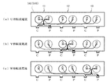
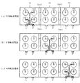
ここで、図12は、図11におけるU相の転流回路を示したものである。なお、V相及びW相についても同様の転流回路によって説明される。 Here, FIG. 12 shows the U-phase commutation circuit in FIG. The V phase and the W phase are also explained by the same commutation circuit.
図12(a)は、出力電流IUが正の場合、すなわち、交流出力端子Uから負荷に向かって電流が流出している場合に、IGBTモジュールQU1のオン→オフ切換時、または、QU1のオフ→オン切換に伴うダイオードモジュールDUのオフ時に形成される転流回路であり、i ,iiは転流電流の経路を示している。
このとき、QU1またはDUには、回路のインダクタンスに起因するサージ電圧が発生する。
FIG. 12A shows a case where the IGBT module QU1 is switched from on to off when the output current IU is positive, that is, when the current is flowing from the AC output terminal U toward the load, or Q a commutation circuit formed when U1 off → diode module D U with the on switching off, i, ii indicates the path of commutation current.
At this time, the Q U1 or D U, surge voltage caused by the inductance of the circuit occurs.
また、図12(b)は、出力電流IUが負の場合、すなわち、負荷から交流出力端子Uに向かって電流が流入している場合に、IGBTモジュールQX2のオン→オフ切換時、または、QX2のオフ→オン切換に伴うダイオードモジュールDXのオフ時に形成される転流回路であり、iii,ivは転流電流の経路を示している。
このとき,QX2またはDXには、回路のインダクタンスに起因するサージ電圧が発生する。
FIG. 12B shows a case where the IGBT module QX2 is switched from on to off when the output current IU is negative, that is, when current flows from the load toward the AC output terminal U, or , Q X2 is a commutation circuit formed when the diode module D X is turned off in accordance with switching from OFF to ON, and iii and iv indicate paths of the commutation current.
At this time, a surge voltage due to the inductance of the circuit is generated in Q X2 or D X.
スイッチング動作に伴って発生するサージ電圧は、上述のように回路のインダクタンスに起因し、モジュール素子を破壊する原因となるため、小さくする必要がある。この原因となる回路のインダクタンスを小さくするためには、前記経路i〜ivに存在するIGBTモジュール、ダイオードモジュール及びフィルタコンデンサ間の配線長を、それぞれ小さくしなければならない。
更に、経路iと経路iii、経路iiと経路ivを見ると、それぞれ、中性点電源端子Cが接続された線(中性点電圧ECの線)を中心線として対称になっているので、正負アームの転流回路が有するインダクタンスの偏差を極力小さくするためには、各経路上のIGBTモジュール、ダイオードモジュール、フィルタコンデンサ、及び電源端子P,C,N、交流出力端子U,V,W、配線用部材等の配置に関して、幾何学的な意味で対称的であることが望ましい。
The surge voltage generated with the switching operation is caused by the inductance of the circuit as described above and causes the module element to be destroyed. Therefore, it is necessary to reduce the surge voltage. In order to reduce the inductance of the circuit that causes this, the wiring length between the IGBT module, the diode module, and the filter capacitor existing in the paths i to iv must be reduced.
Further, when looking at the route i and the route iii and the route ii and the route iv, the lines (neutral point voltage E C lines) to which the neutral point power supply terminals C are connected are symmetric with respect to the center line. In order to minimize the inductance deviation of the commutation circuit of the positive and negative arms, the IGBT module, the diode module, the filter capacitor, and the power supply terminals P, C, N, and the AC output terminals U, V, W on each path It is desirable that the arrangement of wiring members and the like is symmetrical in a geometric sense.
なお、3レベル電力変換装置において、配線インダクタンスを最小化するための素子の配列と素子端子間の配線方法が、特許文献4及び特許文献5に開示されている。
このうち、特許文献4に係る3レベル電力変換装置は、正側アーム、負側アームの両方においてスイッチング素子、結合ダイオード及び直流電圧源をほぼ直線上に配置し、各スイッチング素子及び結合ダイオードの全ての接続部を同一方向に突出させ、この方向と直交し、かつ互いに絶縁された複数の平板状の配線板を用いて、前記接続部間の所定の接続を行うように構成されている。
In the three-level power converter,
Among these, in the three-level power conversion device according to
また、特許文献5に係る3レベル電力変換装置は、複数のスイッチング素子と、結合ダイオードと、直流電圧源(平滑コンデンサ)と、前記スイッチング素子及び直流電圧源に挟まれるように配置される平板状導体と、を備えており、前記スイッチング素子及び結合ダイオードを一列に配置すると共に、平板状導体のほぼ同一箇所の表裏を介して直流電圧源と結合ダイオードとを接続するように構成されている。また、この3レベル電力変換装置では、ターンオフするスイッチング素子の電流が流れる第1の電流路と、この第1の電流路の電流の減少に伴って電流が増大する第2の電流路との配線を沿わせるように構成している。 In addition, the three-level power conversion device according to Patent Document 5 includes a plurality of switching elements, coupling diodes, a DC voltage source (smoothing capacitor), and a flat plate shape disposed so as to be sandwiched between the switching elements and the DC voltage source. The switching element and the coupling diode are arranged in a line, and the DC voltage source and the coupling diode are connected to each other through the front and back of substantially the same portion of the flat conductor. Further, in this three-level power converter, wiring between the first current path through which the current of the switching element to be turned off flows and the second current path in which the current increases as the current in the first current path decreases is provided. It is configured to follow.
特許文献1のように、インバータ等の電力変換装置を構成する各相の回路を別々のユニットとして構成する場合には、回路上の共通電圧の導体がユニットごとに必要となり、装置全体の大形化や重量増加を招く。
また、特許文献2においても、スイッチング素子とフィルタコンデンサとの間の配線長に起因するインダクタンスが大きくなるという問題がある。このインダクタンスはスイッチング動作に伴って大きなサージ電圧を発生させ、素子を破壊する原因となるが、サージ電圧吸収用にスナバ回路を追加すると、スナバ回路の構成部品によってインバータやコンバータのユニットが大形化し、結果的に装置全体が大形化し、重量増加の原因となる。
When each phase circuit constituting a power conversion device such as an inverter is configured as a separate unit as in Patent Document 1, a common voltage conductor on the circuit is required for each unit, and the overall size of the device is large. Cause an increase in weight and weight.
Also in
更に、特許文献4,5に記載された従来技術によれば、配線インダクタンスの低減はある程度可能であるが、装置の小形化等の観点から、フィルタコンデンサの配線構造や両極端子、直流電源端子の配置等に関して更に改良の余地を残している。
Further, according to the prior art described in
そこで、本発明の解決課題は、
(1)フィルタコンデンサを含んだスイッチング素子周りの配線の低インダクタンス化
(2)フィルタコンデンサの配線構造の合理化(部品点数の削減、部品の共通化等)
(3)各相の直流端子及びフィルタコンデンサの両極端子の合理的配置
を行い、装置全体の小形化、軽量化を可能にした3レベル電力変換装置を提供することにある。
Therefore, the problem to be solved by the present invention is:
(1) Lower inductance of the wiring around the switching element including the filter capacitor (2) Rationalization of the wiring structure of the filter capacitor (reduction of the number of parts, sharing of parts, etc.)
(3) To provide a three-level power conversion device in which the DC terminal of each phase and the bipolar terminals of the filter capacitor are rationally arranged to reduce the size and weight of the entire device.
上記課題を解決するため、本発明は、複数相の3レベル変換回路及び複数のフィルタコンデンサを備えた3レベル電力変換装置において、各相の配線インダクタンスを最小化するために、フィルタコンデンサの両極端子を2個の平板導体の重ね配線構造によって直流端子に接続することを基本としている。 In order to solve the above-mentioned problems, the present invention provides a bipolar terminal of a filter capacitor for minimizing the wiring inductance of each phase in a three-level power conversion device including a plurality of three-phase conversion circuits and a plurality of filter capacitors. Is basically connected to a DC terminal by an overlapping wiring structure of two flat conductors.
すなわち、前述の図11に示した3レベルインバータ等の3レベル電力変換装置において、本発明の主な特徴は以下の通りである。
まず、各相の正側アームのフィルタコンデンサCFU,CFV,CFWの両極端子を、全相分一括して、直流正電源端子P及び中性点電源端子Cに接続される2個の平板導体にそれぞれ接続し、これらの平板導体を絶縁板を介して積層配置する(なお、このような2個の平板導体による積層状の配線構造を重ね配線ともいう)。同様に、負側アームのフィルタコンデンサCFX,CFY,CFZの両極端子を、全相分一括して、中性点電源端子C及び直流負電源端子Nに接続される2個の平板導体にそれぞれ接続し、これらの平板導体を絶縁板を介して積層配置する。
That is, the main features of the present invention in the three-level power converter such as the three-level inverter shown in FIG. 11 are as follows.
First, the two pole terminals of the filter capacitors C FU , C FV , C FW of the positive arm of each phase are collectively connected to the DC positive power supply terminal P and the neutral point power supply terminal C for all phases. The flat conductors are respectively connected to the flat conductors, and the flat conductors are laminated via an insulating plate (a laminated wiring structure of two flat conductors is also referred to as a stacked wiring). Similarly, the two flat conductors connected to the neutral point power supply terminal C and the DC negative power supply terminal N are collectively connected to the negative electrode filter capacitors C FX , C FY , and C FZ for all phases. Are connected to each other, and these flat conductors are laminated and disposed via an insulating plate.
また、各相共に正側アーム及び負側アームの配線インダクタンスが均衡して最小値となるように、正側アーム及び負側アームを構成するスイッチング素子モジュールとしてのIGBTモジュールQU1,QU2,QV1,QV2,QW1,QW2,QX1,QX2,QY1,QY2,QZ1,QZ2並びにダイオードモジュールDU,DV,DW,DX,DY,DZを、中性点電圧ECに対応する導体の一点を幾何学的中心点としてほぼ対称となるように配置し、その配線部材も前記幾何学的中心点を中心としてほぼ対称となるように配置する。
更に、直流正電源端子P、中性点電源端子C及び直流負電源端子Nにそれぞれ接続されるフィルタコンデンサの各電源端子は、各相とも前記幾何学的中心点を中心として対称となるように配置し、各相の交流出力端子U,V,Wは前記幾何学的中心点を含む直線上に配置する。
Further, IGBT modules Q U1 , Q U2 , Q as switching element modules constituting the positive side arm and the negative side arm so that the wiring inductances of the positive side arm and the negative side arm are balanced and become the minimum value in each phase. V1, Q V2, Q W1, Q W2, Q X1, Q X2, Q Y1, Q Y2, Q Z1, Q Z2 and diode modules D U, D V, D W , D X, D Y, and D Z, One point of the conductor corresponding to the neutral point voltage E C is arranged so as to be substantially symmetric with respect to the geometric center point, and the wiring member is also arranged so as to be substantially symmetric with respect to the geometric center point.
Further, the power supply terminals of the filter capacitors connected to the DC positive power supply terminal P, the neutral point power supply terminal C, and the DC negative power supply terminal N are symmetric with respect to the geometric center point in each phase. The AC output terminals U, V, W of each phase are arranged on a straight line including the geometric center point.
また、電源端子P,C,N及び交流出力端子U,V,Wについては、フィルタコンデンサCFU,CFV,CFW,CFX,CFY,CFZの平板導体による重ね配線化と外部端子配線の広幅導体による重ね配線化を行うために、適正な位置決めを行う。 Further, for the power supply terminals P, C, N and the AC output terminals U, V, W, overlapping wiring by a flat conductor of filter capacitors C FU , C FV , C FW , C FX , C FY , C FZ and external terminals Appropriate positioning is performed in order to achieve overlapping wiring with a wide conductor of wiring.
各相の3レベル変換回路MU,MV,MWの素子間を接続するための積層配線部は、正側アームと負側アームとの中間部でスイッチング素子等の素子群とは反対側に突出した凸部を備えている。この凸部の表面には、3レベル変換回路MU,MV,MWの電源端子P,C,Nにそれぞれ接続されるフィルタコンデンサの各電源端子を、また、裏面には交流出力端子U,V,Wを、正側アームと負側アームとの中間線上の特定点を中心点として対称となる位置に配置する。 Laminated wiring portion for connecting the elements of each phase of the three-level converter circuit M U, M V, M W is the side opposite to the element group such as a switching element at an intermediate portion between the positive side arm and the negative-side arm Has a protruding part. On the surface of the convex portion, three-level converter circuit M U, M V, the power supply terminal P of M W, C, each power terminal of the filter capacitor connected respectively to N, also on the back AC output terminal U , V, W are arranged at symmetrical positions with a specific point on the intermediate line between the positive side arm and the negative side arm as a center point.
各相の3レベル変換回路MU,MV,MWを構成するスイッチング素子の転流時に発生する転流電流が、相間で相互に分流するのを阻止して転流電流を各相で均一化するために、隣接する相のフィルタコンデンサ間の平板導体の所定位置に、分流電流を抑制するための切り欠き部をそれぞれ設ける。 Each phase of a three-level converter circuit M U, M V, uniform commutation currents generated upon commutation of the switching elements constituting the M W is, the commutation current is prevented from shunting each other between phases with each phase In order to achieve this, a notch for suppressing the shunt current is provided at a predetermined position of the flat conductor between the filter capacitors of adjacent phases.
フィルタコンデンサが各アーム当たり1個で構成される場合には、各フィルタコンデンサの両極端子の配列方向を、積層配線部の表面に対して平行にする。
また、フィルタコンデンサが各アーム当たり複数個のコンデンサユニットにて構成される場合には、各コンデンサユニットの両極端子の配列方向を、積層配線部の表面に対して垂直にする。更に、隣接するコンデンサユニットの両極端子の極性が交互に変わるように配置する。
In the case where one filter capacitor is configured for each arm, the arrangement direction of the bipolar terminals of each filter capacitor is made parallel to the surface of the multilayer wiring portion.
When the filter capacitor is composed of a plurality of capacitor units per arm, the arrangement direction of the bipolar terminals of each capacitor unit is made perpendicular to the surface of the multilayer wiring portion. Furthermore, it arrange | positions so that the polarity of the bipolar terminal of an adjacent capacitor | condenser unit may change alternately.
通常、3相インバータの場合、フィルタコンデンサは各アーム当たり少なくとも1個設置されるから、電源端子P,C,Nからフィルタコンデンサまでの配線数は1相あたり最小で3本必要となり、3相では最小で9本必要となる。また、2相コンバータの場合でも電源端子P,C,Nからフィルタコンデンサまでの配線数は1相当たり最小で3本必要となり、2相では最小で6本必要となる。 Normally, in the case of a three-phase inverter, since at least one filter capacitor is installed for each arm, the minimum number of wires from the power terminals P, C, N to the filter capacitor is required per phase. A minimum of 9 is required. Even in the case of a two-phase converter, the minimum number of wires from the power terminals P, C, N to the filter capacitor is three per phase, and the minimum is six for two phases.
これに対し、本発明によれば、電源端子P,C,Nから一括して平板導体による重ね配線となるので、配線のインダクタンスが低減される。更に、電源端子P,C,Nからフィルタコンデンサまでの配線数は、インバータ等の相数に関係なく正側アーム用が2個、負側アーム用が2個で計4個となり、部品点数の低減と部品の共通化が可能となり、配線の簡単化、組み立て工数の低減、装置の小形・コンパクト化、軽量化が可能となる。 On the other hand, according to the present invention, since the wiring is formed by the flat conductors collectively from the power terminals P, C, N, the inductance of the wiring is reduced. Furthermore, the number of wires from the power terminals P, C, N to the filter capacitor is 4 for the positive arm and 2 for the negative arm regardless of the number of phases of the inverter, etc. Reduction and standardization of parts are possible, simplifying wiring, reducing assembly man-hours, making the device compact, compact, and lightweight.
各相のスイッチング素子、結合ダイオード、電源端子、交流出力端子等の配線は幾何学的中心点を中心としてすべての相が対称的に配置され、正側アーム用,負側アーム用フィルタコンデンサも同様に対称的に配置されるので、転流ループのインダクタンスの最小化と均一化が可能になる。
従って、各アームのスイッチング素子は、スナバ回路を付加しなくても、充分小さいサージ電圧でスイッチングすることができる。更に、2枚重ねの平板導体とこれらに挟まれた絶縁板とは、両アームとも同一形状、同一構造であるから、部品の共通化と部品点数の削減に有効である。
All phase switching elements, coupling diodes, power supply terminals, AC output terminals, etc. are arranged symmetrically around the geometric center point, and the same applies to the positive and negative arm filter capacitors. Therefore, the inductance of the commutation loop can be minimized and made uniform.
Therefore, the switching element of each arm can be switched with a sufficiently small surge voltage without adding a snubber circuit. Furthermore, the two-layer flat plate conductor and the insulating plate sandwiched between them have the same shape and the same structure in both arms, and thus are effective in sharing parts and reducing the number of parts.
各相の電源端子及び交流出力端子は、直流電圧の配線及び交流電圧の配線を広幅の平板導体による重ね配線を行うために最も効果的な位置に設けられるので、電源及び交流出力の配線インダクタンスを低減でき、近傍の電子回路への誘導障害が低減される。 The power supply terminals and AC output terminals of each phase are provided at the most effective positions for the wiring of the DC voltage and the wiring of the AC voltage with the wide flat conductors, so that the wiring inductance of the power supply and the AC output is reduced. Inductive interference to nearby electronic circuits can be reduced.
以下、図に沿って本発明の実施形態を説明する。なお、以下の実施形態は、本発明を3相の3レベルインバータに適用した場合のものである。
まず、図1は、3相の3レベルインバータの各相について、図12に示した転流回路のインダクタンスを最小化するためのフィルタコンデンサの配置構造及び接続状態を説明するための配線図である。
Hereinafter, embodiments of the present invention will be described with reference to the drawings. In the following embodiments, the present invention is applied to a three-phase three-level inverter.
First, FIG. 1 is a wiring diagram for explaining a filter capacitor arrangement structure and connection state for minimizing the inductance of the commutation circuit shown in FIG. 12 for each phase of a three-phase three-level inverter. .
図1において、1,2,3はそれぞれU相,V相,W相3レベル変換回路であり、図11における各相3レベル変換回路MU,MV,MWに相当する。各3レベル変換回路1〜3は、U相,V相,W相IGBTモジュール11〜14,21〜24,31〜34、U相,V相,W相ダイオードモジュール15,16、25,26、35,36から構成されている。
In FIG. 1,
4は正側アーム用フィルタコンデンサ接続回路であり、正側アーム用U,V,W相フィルタコンデンサ41,42,43と、これらを並列接続する2個の正側アーム用フィルタコンデンサ接続平板導体101,102とからなっている。なお、平板導体101を正電源平板導体、102を中性点電源平板導体ともいう。上記フィルタコンデンサ41,42,43は、図11におけるフィルタコンデンサCFU,CFV,CFWに相当する。
前記平板導体101には、U,V,W相フィルタコンデンサ直流電源端子111,211,311が設けられ、平板導体102には、U,V,W相フィルタコンデンサ直流電源端子112,212,312が設けられている。
The
一方、5は負側アーム用フィルタコンデンサ接続回路であり、負側アーム用U,V,W相フィルタコンデンサ51,52,53と、これらを並列接続する2個の負側アーム用フィルタコンデンサ接続平板導体103,104とからなっている。なお、平板導体103を中性点電源平板導体、104を負電源平板導体ともいう。上記フィルタコンデンサ51,52,53は、図11におけるフィルタコンデンサCFX,CFY,CFZに相当する。
前記平板導体103には、U,V,W相フィルタコンデンサ直流電源端子113,213,313が設けられ、平板導体104には、U,V,W相フィルタコンデンサ直流電源端子114,214,314が設けられている。
On the other hand, reference numeral 5 denotes a negative arm filter capacitor connection circuit, which is a negative arm U, V, W
The
ここで、U,V,W相フィルタコンデンサ直流電源端子111,211,311は、後述する積層配線部503上の導体を介して直流正電源端子Pに接続され、U,V,W相フィルタコンデンサ直流電源端子114,214,314は同じく直流負電源端子Nに接続されている。同時に、直流電源端子111,211,311はIGBTモジュール11,21,31のコレクタに、直流電源端子114,214,314はIGBTモジュール14,24,34のエミッタにも接続されている。
また、U,V,W相フィルタコンデンサ直流電源端子112,212,312,113,213,313は、後述する積層配線部503上の導体を介して中性点電源端子Cに接続されている。
更に、各相3レベル変換回路1,2,3の正側アームと負側アームとの接続点は、U,V,W相交流出力端子115,215,315となっている。
Here, the U, V, and W phase filter capacitor DC
The U, V, and W phase filter capacitor DC
Furthermore, the connection points between the positive side arm and the negative side arm of each phase three-
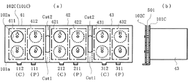
次に、図2は、図1の配線図に対応する3レベルインバータのパワーユニットの構造図であり、図2(a)は正面図、図2(b)は図2(a)の右側面図である。
図2(a)において、CLU,CLV,CLWは、それぞれ正側アーム用U,V,W相フィルタコンデンサ41,42,43、負側アーム用U,V,W相フィルタコンデンサ51,52,53の中心を通るU,V,W相中心線であり、CLCは正負アームの中間点を通る中間線である。また、平板導体101〜104及び各相の電源端子111〜114,211〜214,311〜314は、各端子の位置関係を明示するため上下方向に離れた位置に描かれているが、実際は正負アーム中間線CLCに近接して配置される。特に、平板導体101,102及び103,104は、それぞれ2枚重ねされて積層構造となっている。
Next, FIG. 2 is a structural diagram of a power unit of a three-level inverter corresponding to the wiring diagram of FIG. 1, FIG. 2 (a) is a front view, and FIG. 2 (b) is a right side view of FIG. It is.
In FIG. 2A, CL U , CL V , and CL W are U, V, W
なお、図2(b)において、501は平板導体101,102間を絶縁する絶縁板、502は平板導体103,104間を絶縁する絶縁板、503は表裏の導体相互間に絶縁板を挟んで形成したプリント基板等の積層配線部、504はIGBTモジュールやダイオードモジュール(図示せず)が実装され、かつ積層配線部503及び平板導体101〜104を介してフィルタコンデンサ41〜43,51〜53や各相の電源端子111〜114,211〜214,311〜314、各相交流出力端子115,215,315に接続されるモジュール取付部、505は放熱のための冷却体受熱部である。
In FIG. 2B, 501 is an insulating plate that insulates between the
更に詳述すると、正側アーム用のフィルタコンデンサ41,42,43及び負側アーム用のフィルタコンデンサ51,52,53は、それぞれ2枚重ねの平板導体101,102及び103,104によりアームごとに並列接続されている。また、平板導体101は、直線上に配置されて積層配線部503上の導体により互いに導通している電源端子111,211,311に、平板導体102,103は同じく直線上に配置されて互いに導通している電源端子112,212,312及び113,213,313に、平板導体104は同じく直線上に配置されて互いに導通している電源端子114,214,314に、それぞれ接続されている。
More specifically, the
図2(a)から明らかなように、正側アーム用フィルタコンデンサ接続回路4内のフィルタコンデンサ41〜43と負側アーム用フィルタコンデンサ接続回路5内のフィルタコンデンサ51〜53、及び各相の電源端子111〜114,211〜214,311〜314は、V相3レベル変換回路2の中心点、すなわち、正負アーム中間線CLCとV相中心線CLVとの交点を中心にして、180度回転した位置(点対称)となるように対称に配置される。
更に、電源端子111〜114,211〜214,311〜314については各相ともに、その相の中心線と正負アーム中間線CLCとの交点を中心にして点対称となるように、例えばU相の場合、電源端子111,112と電源端子114,113とは、U相中心線CLUと正負アーム中間線CLCとの交点を中心にして点対称となるように配置されている。
As apparent from FIG. 2A, the
Furthermore, each phase both for the
また、図2(b)には示されていないが、各相3レベル変換回路1〜3を構成するIGBTモジュール11〜14,21〜24,31〜34及びダイオードモジュール15,16、25,26、35,36も、前記モジュール取付部504において、各相とも正側アーム、負側アームの中間点を中心にして180度回転した位置となるように対称に配置されており、モジュールの端子間配線を最も合理的に配置できる位置に装着されている。
Although not shown in FIG. 2 (b), the
各モジュールの端子は、積層配線部503の中心部において各モジュールとは反対側(平板導体101〜104側)に突出した凸部503aに集約されている。この凸部503aの表面の導体には、各相の電源端子111,211,311(図2(b)では便宜上、符号311のみを表記する)、112,113,212,213,312,313(同じく符号313のみを表記する)、114,214,314(同じく符号314のみを表記する)が配置され、裏面の正負アーム中間線CLCと各相中心線CLU,CLV,CLWとの交点には、各相の交流出力端子115,215,315がそれぞれ配置される。
交流出力端子115,215,315を上記の位置に配置することにより、積層配線部503上の出力電流を平面的に平準化することができる。
The terminals of each module are gathered at a
By arranging the
なお、この実施形態において、積層配線部503の表面側では、平板導体101〜104と各電源端子P,N,Cとが各相につきそれぞれ1個の電源端子により接続される例を示しているが、複数の電源端子により接続しても良い。同様に、裏面側の交流出力端子115,215,315についても、それぞれ複数の出力端子によって構成しても良い。
In the present embodiment, on the surface side of the
次に、図3は、この実施形態における積層配線部503の各電源端子P,C,Nと、交流出力端子115,215,315に接続された各相の交流出力端子U,V,Wの配線状態を示している。
図3に示すように、積層配線部503の裏面において、交流出力端子115,215,315を正負アーム中間線CLCと各相中心線CLU,CLV,CLWとの交点にそれぞれ配置し、広幅導体510を相間の隙間から上面に出して重ね配線することにより、電源端子111,211,311,112,113,212,213,312,313,114,214,314と各電源端子P,C,Nとを接続する広幅導体511と区分可能としている。
Next, FIG. 3 shows the power supply terminals P, C, N of the
As shown in FIG. 3, the rear surface of the
各相の端子をこのように配置することにより、パワーユニットの外線端子、すなわち、各電源端子P,C,N及び交流出力端子U,V,Wに至る広幅導体510,511を重ねて構成することができ、電源及び交流出力の配線インダクタンスを小さくして近傍の電子回路への誘導障害を低減することができる。
By arranging the terminals of each phase in this way, the
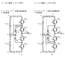
図4(a)は図2(a)のY−Y断面図、図4(b)は図4(a)の右側面図であり、正側アーム用U,V,W相フィルタコンデンサ41〜43と正側アーム用フィルタコンデンサ接続平板導体101,102との接続状態を示している。なお、A,Bはフィルタコンデンサ41〜43の両極端子であり、一方が正極端子、他方が負極端子である。
ここで、図4に示す平板導体101,102を平板導体の第1実施例というものとする。
4A is a cross-sectional view taken along line YY of FIG. 2A, and FIG. 4B is a right side view of FIG. 4A. U, V, W-
Here, the
図4に示すフィルタコンデンサ41〜43及び平板導体101,102の接続構造を、例えば接続端子112を中心として180°回転させれば、負側アーム用U,V,W相フィルタコンデンサ51〜53と負側アーム用フィルタコンデンサ接続平板導体104,103との接続構造と実質的に同様になる。言い換えれば、平板導体101,104及び102,103の形状、構造をそれぞれ同一にすることができる。
このことは、後述する平板導体の第2実施例〜第4実施例においても同様である。
ここで、平板導体による重ね配線構造及び転流電流の流れは正側、負側で全く同様であるため、以下では正側アームについて平板導体101,102による重ね配線の特徴を説明する。
If the connection structure of the
This is the same in the second to fourth embodiments of the flat plate conductor described later.
Here, since the overlapping wiring structure by the flat plate conductor and the flow of the commutation current are exactly the same on the positive side and the negative side, the characteristics of the overlapping wiring by the
図4において、各相のフィルタコンデンサ41〜43の端子Aは正電源用の平板導体101に接続され、端子Bは中性点電源用の平板導体102に接続されている。また、平板導体101,102の間には、両導体間の印加電圧に充分に耐えると共にできるだけ薄い絶縁板501を挟むことにより、フィルタコンデンサに至る配線のインダクタンスを最小化する。
更に、端子Bと平板導体101との間の耐圧、端子Aと平板導体102との間の耐圧にそれぞれ充分耐えるように空間距離を保有させるための孔101a,102aが、平板導体101,102に設けられている。
正電源用の平板導体101には、前記積層配線部503の正電源端子Pに接続される電源端子111,211,311が、中性点電源用の平板導体102には、積層配線部503の中性点電源端子Cに接続される電源端子112,212,312がそれぞれ設けられている。
In FIG. 4, the terminals A of the
Furthermore,
The
次に、図5は、図12(a)における転流電流の経路iを、平板導体101,102上の電流経路として単線で示したものである。図5において、太線は転流相フィルタコンデンサへの主電流を、細線は他相フィルタコンデンサへの分流電流を示し、実線は手前の平板導体102上の電流を、点線は背後の平板導体101上の電流を示す。
Next, FIG. 5 shows the path i of the commutation current in FIG. 12A as a current path on the
図5に示すように、実線の電流と点線の電流とは、電磁作用により平板導体101,102上をペアで重なって端子A,Bと電源端子P,Cとの間を流れるので、これらの端子間のインダクタンスは効果的に低減される。なお、図12(b)における転流電流の経路ivについても、同様に説明することができる。
前述したように、負側アームは正側アームと対称的に配置・配線されているので、図12(a),(b)における負側アームのフィルタコンデンサの転流電流の経路ii,iiiについても、正側アームと同様に説明可能である。
As shown in FIG. 5, the solid line current and the dotted line current flow between the terminals A and B and the power supply terminals P and C by overlapping with each other on the
As described above, since the negative arm is arranged and wired symmetrically with the positive arm, the commutation current paths ii and iii of the filter capacitor of the negative arm in FIGS. This can be explained in the same manner as the positive side arm.
なお、図5では、説明を単純化するために転流電流を単線で示してあるが、点線で示す正電源用の平板導体101上の電流と、実線で示す中性点電源用の平板導体102上の電流は、実際はに各相のフィルタコンデンサの端子A,Bと電源端子P,Cとの幾何学的配置関係によって決まる幅状電流となって、両平板導体101,102上を互いに逆方向に流れる。このように幅状電流が流れることにより、配線インダクタンスは一層効果的に低減される。
また、以下に説明する第2〜第4実施例においても転流電流を単線で示すが、実際の電流はコンデンサ端子と電源端子との幾何学的配置関係によって決まる幅状電流となる。
In FIG. 5, the commutation current is shown as a single line for simplicity of explanation, but the current on the positive power supply
Also, in the second to fourth embodiments described below, the commutation current is indicated by a single line, but the actual current is a width-like current determined by the geometrical relationship between the capacitor terminal and the power supply terminal.
次に、図6は平板導体の第2実施例を示している。この実施例では、図5に細線で示した他相フィルタコンデンサへの分流電流を低減して各相の電流を均一化するために、平板導体101A,102Aにそれぞれ切り欠き部Cut1,Cut2を設けてある。
すなわち、図6では、各電源端子111〜312の近傍に切り欠き部Cut1,Cut2を設けることにより、平板導体101A,102Aの各相間下部の分流電流の経路を遮断するようにした。
FIG. 6 shows a second embodiment of the flat conductor. In this embodiment, the
That is, in FIG. 6, by providing the notches Cut1 and Cut2 in the vicinity of each of the
また、図7は平板導体の第3実施例を示している。この実施例では、各相のフィルタコンデンサ41〜43の相互間において、平板導体101Bでは下部に、平板導体102Bでは上部に、それぞれ切り欠き部Cut1,Cut2を設けたものである。
このように切り欠き部Cut1,Cut2によって平板導体101B,102Bの各相間に空隙部を形成することにより、分流電流がペアとなって重なって流れるのを抑制することができる。
FIG. 7 shows a third embodiment of the flat conductor. In this embodiment, notch portions Cut1 and Cut2 are provided between the
Thus, by forming a gap between the phases of the
なお、以上の説明は、フィルタコンデンサが各アーム当たり1個で構成される場合のものである。この場合、図4〜図7に示したように、コンデンサの両極端子A,Bの配列方向は、平板導体101(101A,101B),102(102A,102B)の電源端子111〜312が接続される図2(b)の積層配線部503(凸部503a)の表面に対して平行になっている。これにより、平板導体101(101A,101B),102(102A,102B)上の電流経路が対称的かつ最短となる。
The above explanation is for a case where one filter capacitor is formed for each arm. In this case, as shown in FIGS. 4 to 7, the
次いで、図8は平板導体の第4実施例を示しており、フィルタコンデンサが各アーム当たり複数個(図8では2個)のコンデンサユニットにより構成される場合のものである。すなわち、フィルタコンデンサ41〜43は、互いに並列接続されたコンデンサユニット411,412、421,422、431,432によってそれぞれ構成されている。
Next, FIG. 8 shows a fourth embodiment of the flat conductor, in which the filter capacitor is composed of a plurality (two in FIG. 8) of capacitor units for each arm. That is, the
この場合、フィルタコンデンサ41〜43はアームごとに隣接して配置され、各コンデンサユニット411,412、421,422、431,432の両極端子A,Bの配列方向は、平板導体101C,102Cの電源端子111〜312が取り付けられる図2(b)の積層配線部503(凸部503a)の表面に対して垂直になっている。また、相隣り合うコンデンサユニットは、端子A,Bが交互に配置されており、全ての端子は直線上で2列に整列して平板導体101C,102Cに接続されている。
なお、図8においても、図7と同様に分流電流を抑制するための切り欠き部Cut1,Cut2が、平板導体101C,102Cの各相間に形成されている。
In this case, the
In FIG. 8, notches Cut1 and Cut2 for suppressing the shunt current are formed between the phases of the
図9は、この実施例における各相電流の平板導体101C,102C上の電流経路を示している。
フィルタコンデンサ41〜43を構成するコンデンサユニット411,412、421,422、431,432は、それぞれ異極性の端子A,Bが隣り合うように順次配置されているため、上側の端子を流れる電流と下側の端子を流れる電流とが逆向きになり、これらの電流がペアを構成して重なって流れることになるので、配線のインダクタンスが効果的に低減されることになる。
FIG. 9 shows current paths on the
Since the
なお、上述した実施形態では本発明を3相3レベルインバータに適用した場合について説明したが、2相3レベルコンバータの場合も、前記同様のフィルタコンデンサ、平板導体及び積層配線部等の配線構造、接続構造を適用することができる。また、各アームを構成するスイッチング素子及び結合ダイオードがそれぞれ複数の並列接続によって使用される場合にも、同様の配線構造、接続構造を適用可能である。 In the above-described embodiment, the case where the present invention is applied to a three-phase three-level inverter has been described. However, in the case of a two-phase three-level converter, a wiring structure such as a filter capacitor, a flat conductor, and a laminated wiring section similar to the above- A connection structure can be applied. Further, when the switching elements and the coupling diodes constituting each arm are used by a plurality of parallel connections, the same wiring structure and connection structure can be applied.
1:U相3レベル変換回路
2:V相3レベル変換回路
3:W相3レベル変換回路
4:正側アーム用フィルタコンデンサ接続回路
5:負側アーム用フィルタコンデンサ接続回路
11〜14:U相IGBTモジュール
21〜24:V相IGBTモジュール
31〜34:W相IGBTモジュール
15,16:U相ダイオードモジュール
25,26:V相ダイオードモジュール
35,36:W相ダイオードモジュール
41,42,43:正側アーム用U,V,W相フィルタコンデンサ
51,52,53:負側アーム用U,V,W相フィルタコンデンサ
101,102,101A,102A,101B,102B,101C,102C:正側アーム用フィルタコンデンサ接続平板導体
101a,102a:孔
103,104:負側アーム用フィルタコンデンサ接続平板導体
(101:正電源平板導体,104:負電源平板導体,102,103:中性点電源平板導体)
111〜114:U相フィルタコンデンサ直流電源端子
211〜214:V相フィルタコンデンサ直流電源端子
311〜314:W相フィルタコンデンサ直流電源端子
115:U相出力端子
215:V相出力端子
315:W相出力端子
411,412,421,422,431,432:コンデンサユニット
501,502:絶縁板
503:積層配線部
503a:凸部
504:モジュール取付部
505:冷却体受熱部
510,511:広幅導体
P,C,N:電源端子
U,V,W:交流出力端子
A,B:端子
CLC:正負アーム中間線
CLU:U相中心線
CLV:V相中心線
CLW:W相中心線
Cut1,Cut2:切り欠き部
1:
111 to 114: U phase filter capacitor DC
Claims (5)
前記3レベル変換回路を構成するスイッチング素子及び結合ダイオード素子を全相共通の冷却体受熱部に装着し、導体相互間に絶縁板を挟んで形成した積層配線部により前記各素子の端子間を接続すると共に、前記積層配線部に近接して配置された前記フィルタコンデンサを前記3レベル変換回路の直流端子に接続してなる3レベル電力変換装置において、
各相の前記フィルタコンデンサを正アーム側及び負アーム側に分けて配置し、各アーム側において、各フィルタコンデンサの同一極性の端子同士を前記直流端子に接続するための2個の平板導体を、絶縁板を挟んで積層して配置すると共に、
前記積層配線部は、正側アームと負側アームとの間で前記各素子とは反対側に突出した凸部を備え、この凸部の表面に前記3レベル変換回路の各相直流端子が、裏面には交流端子が、正側アームと負側アームとの中間線上の特定点を中心として対称の位置に配置され、前記各相直流端子をそれぞれ対応する前記平板導体に接続したことを特徴とする3レベル電力変換装置。 A plurality of three-level conversion circuits, and a plurality of filter capacitors provided corresponding to these three-level conversion circuits,
A switching element and a coupling diode element constituting the three-level conversion circuit are mounted on a cooling body heat receiving part common to all phases, and the terminals of each element are connected by a laminated wiring part formed by sandwiching an insulating plate between conductors. And a three-level power conversion device in which the filter capacitor disposed in the vicinity of the multilayer wiring portion is connected to a DC terminal of the three-level conversion circuit.
The filter capacitors of each phase are arranged separately on the positive arm side and the negative arm side, and on each arm side, two flat conductors for connecting the terminals of the same polarity of each filter capacitor to the DC terminal, Lay out the insulating plates and arrange them,
The laminated wiring portion includes a convex portion that protrudes on the opposite side of each element between the positive side arm and the negative side arm, and each phase DC terminal of the three-level conversion circuit on the surface of the convex portion, An AC terminal is arranged on the back surface at a symmetrical position around a specific point on the intermediate line between the positive side arm and the negative side arm, and each phase DC terminal is connected to the corresponding flat plate conductor. A three-level power converter.
正アーム側及び負アーム側の前記平板導体並びに前記絶縁板が、同一形状、同一構造であることを特徴とする3レベル電力変換装置。 The three-level power converter according to claim 1,
3. The three-level power converter according to claim 1 , wherein the flat arm and the insulating plate on the positive arm side and the negative arm side have the same shape and the same structure .
前記平板導体に、ある相の直流端子から他相のフィルタコンデンサの端子に流れる分流電流を低減させるための切り欠き部を設けたことを特徴とする3レベル電力変換装置。 In the three-level power converter according to claim 1 or 2,
3. A three-level power converter according to claim 1, wherein a cutout portion for reducing a shunt current flowing from a DC terminal of one phase to a terminal of a filter capacitor of another phase is provided in the flat conductor .
フィルタコンデンサが各アーム当たり1個で構成される場合に、各フィルタコンデンサの両極端子の配列方向を、前記積層配線部の表面に対して平行にしたことを特徴とする3レベル電力変換装置。 In the 3 level power converter device given in any 1 paragraph of Claims 1-3 ,
3. A three-level power converter according to claim 1, wherein when one filter capacitor is formed for each arm, the arrangement direction of the bipolar terminals of each filter capacitor is parallel to the surface of the multilayer wiring portion .
フィルタコンデンサが各アーム当たり複数個のコンデンサユニットにて構成される場合に、各コンデンサユニットの両極端子の配列方向を、前記積層配線部の表面に対して垂直にしたことを特徴とする3レベル電力変換装置。
The three-level power converter according to any one of claims 1 to 3 ,
3-level power filter capacitor to be composed in each arm hit multiple pieces of capacitor unit, the arrangement direction of the extremes terminal of each capacitor unit, characterized in that the perpendicular to the surface of the laminated wiring portion Conversion device.
Priority Applications (1)
| Application Number | Priority Date | Filing Date | Title |
|---|---|---|---|
| JP2007217764A JP4968528B2 (en) | 2007-08-24 | 2007-08-24 | 3-level power converter |
Applications Claiming Priority (1)
| Application Number | Priority Date | Filing Date | Title |
|---|---|---|---|
| JP2007217764A JP4968528B2 (en) | 2007-08-24 | 2007-08-24 | 3-level power converter |
Publications (2)
| Publication Number | Publication Date |
|---|---|
| JP2009055664A JP2009055664A (en) | 2009-03-12 |
| JP4968528B2 true JP4968528B2 (en) | 2012-07-04 |
Family
ID=40506245
Family Applications (1)
| Application Number | Title | Priority Date | Filing Date |
|---|---|---|---|
| JP2007217764A Active JP4968528B2 (en) | 2007-08-24 | 2007-08-24 | 3-level power converter |
Country Status (1)
| Country | Link |
|---|---|
| JP (1) | JP4968528B2 (en) |
Cited By (1)
| Publication number | Priority date | Publication date | Assignee | Title |
|---|---|---|---|---|
| WO2022179966A1 (en) * | 2021-02-24 | 2022-09-01 | Danfoss Silicon Power Gmbh | Conductor structure |
Families Citing this family (4)
| Publication number | Priority date | Publication date | Assignee | Title |
|---|---|---|---|---|
| CN101917133B (en) * | 2010-08-30 | 2012-08-22 | 南京航空航天大学 | Five-electrical level inverter |
| KR101521397B1 (en) * | 2011-08-30 | 2015-05-18 | 미쓰비시덴키 가부시키가이샤 | Semiconductor device |
| JP6575072B2 (en) * | 2015-02-03 | 2019-09-18 | 富士電機株式会社 | Phase unit and three-level power converter using the same |
| JP6764112B2 (en) * | 2016-08-12 | 2020-09-30 | ミツミ電機株式会社 | Battery protection device |
Family Cites Families (3)
| Publication number | Priority date | Publication date | Assignee | Title |
|---|---|---|---|---|
| JPH10201249A (en) * | 1996-12-27 | 1998-07-31 | Shinko Electric Co Ltd | Power module stack for 3-level inverter |
| JP3229931B2 (en) * | 1997-09-08 | 2001-11-19 | 三菱電機株式会社 | 3-level power converter |
| WO2001031771A1 (en) * | 1999-10-27 | 2001-05-03 | Hitachi, Ltd. | Electric power converter |
-
2007
- 2007-08-24 JP JP2007217764A patent/JP4968528B2/en active Active
Cited By (1)
| Publication number | Priority date | Publication date | Assignee | Title |
|---|---|---|---|---|
| WO2022179966A1 (en) * | 2021-02-24 | 2022-09-01 | Danfoss Silicon Power Gmbh | Conductor structure |
Also Published As
| Publication number | Publication date |
|---|---|
| JP2009055664A (en) | 2009-03-12 |
Similar Documents
| Publication | Publication Date | Title |
|---|---|---|
| US10170953B2 (en) | Planar composite structures and assemblies for axial flux motors and generators | |
| JP3906440B2 (en) | Semiconductor power converter | |
| JP4920677B2 (en) | Power conversion device and assembly method thereof | |
| JP3424532B2 (en) | Power converter | |
| US6456516B1 (en) | Provision of a low-inductive rail for three-point phase module | |
| JP5132175B2 (en) | Power converter | |
| US9054599B2 (en) | Power converter and integrated DC choke therefor | |
| JP4968528B2 (en) | 3-level power converter | |
| JP2019110228A (en) | Power conversion device | |
| JP7263891B2 (en) | power converter | |
| JP2012165611A (en) | Semiconductor unit and power conversion device | |
| WO2019043849A1 (en) | Main circuit wiring member and power conversion device | |
| JP4356434B2 (en) | 3-level inverter circuit | |
| US10284111B2 (en) | Power conversion apparatus having connection conductors having inductance which inhibits ripple current | |
| JP6902121B2 (en) | Electric railroad vehicle equipped with a power converter and a power converter | |
| JP6109630B2 (en) | Wiring structure of semiconductor element and power conversion device | |
| EP3562023B1 (en) | Power conversion device | |
| CN112055938B (en) | Power conversion device and power conversion unit | |
| JP2017112682A (en) | Three-level power conversion device | |
| JP5012233B2 (en) | Power converter and method for connecting laminated wiring conductor | |
| JP4828170B2 (en) | Power converter | |
| EP3934085B1 (en) | Power conversion apparatus | |
| JP6976390B1 (en) | Semiconductor devices and power converters | |
| JP6440511B2 (en) | Rotating machine drive | |
| JP2023018359A (en) | power converter |
Legal Events
| Date | Code | Title | Description |
|---|---|---|---|
| A621 | Written request for application examination |
Free format text: JAPANESE INTERMEDIATE CODE: A621 Effective date: 20100118 |
|
| A711 | Notification of change in applicant |
Free format text: JAPANESE INTERMEDIATE CODE: A712 Effective date: 20110422 |
|
| A131 | Notification of reasons for refusal |
Free format text: JAPANESE INTERMEDIATE CODE: A131 Effective date: 20120117 |
|
| A977 | Report on retrieval |
Free format text: JAPANESE INTERMEDIATE CODE: A971007 Effective date: 20120118 |
|
| A521 | Request for written amendment filed |
Free format text: JAPANESE INTERMEDIATE CODE: A523 Effective date: 20120222 |
|
| TRDD | Decision of grant or rejection written | ||
| A01 | Written decision to grant a patent or to grant a registration (utility model) |
Free format text: JAPANESE INTERMEDIATE CODE: A01 Effective date: 20120308 |
|
| A01 | Written decision to grant a patent or to grant a registration (utility model) |
Free format text: JAPANESE INTERMEDIATE CODE: A01 |
|
| A61 | First payment of annual fees (during grant procedure) |
Free format text: JAPANESE INTERMEDIATE CODE: A61 Effective date: 20120321 |
|
| FPAY | Renewal fee payment (event date is renewal date of database) |
Free format text: PAYMENT UNTIL: 20150413 Year of fee payment: 3 |
|
| R150 | Certificate of patent or registration of utility model |
Ref document number: 4968528 Country of ref document: JP Free format text: JAPANESE INTERMEDIATE CODE: R150 Free format text: JAPANESE INTERMEDIATE CODE: R150 |
|
| R250 | Receipt of annual fees |
Free format text: JAPANESE INTERMEDIATE CODE: R250 |
|
| R250 | Receipt of annual fees |
Free format text: JAPANESE INTERMEDIATE CODE: R250 |
|
| R250 | Receipt of annual fees |
Free format text: JAPANESE INTERMEDIATE CODE: R250 |
|
| R250 | Receipt of annual fees |
Free format text: JAPANESE INTERMEDIATE CODE: R250 |
|
| R250 | Receipt of annual fees |
Free format text: JAPANESE INTERMEDIATE CODE: R250 |
|
| R250 | Receipt of annual fees |
Free format text: JAPANESE INTERMEDIATE CODE: R250 |
|
| R250 | Receipt of annual fees |
Free format text: JAPANESE INTERMEDIATE CODE: R250 |
|
| R250 | Receipt of annual fees |
Free format text: JAPANESE INTERMEDIATE CODE: R250 |
|
| RD02 | Notification of acceptance of power of attorney |
Free format text: JAPANESE INTERMEDIATE CODE: R3D02 |
|
| R250 | Receipt of annual fees |
Free format text: JAPANESE INTERMEDIATE CODE: R250 |
|
| R250 | Receipt of annual fees |
Free format text: JAPANESE INTERMEDIATE CODE: R250 |