JP4952148B2 - Semiconductor device and manufacturing method thereof - Google Patents
Semiconductor device and manufacturing method thereof Download PDFInfo
- Publication number
- JP4952148B2 JP4952148B2 JP2006231966A JP2006231966A JP4952148B2 JP 4952148 B2 JP4952148 B2 JP 4952148B2 JP 2006231966 A JP2006231966 A JP 2006231966A JP 2006231966 A JP2006231966 A JP 2006231966A JP 4952148 B2 JP4952148 B2 JP 4952148B2
- Authority
- JP
- Japan
- Prior art keywords
- film
- conductive
- conductive layer
- forming
- insulating film
- Prior art date
- Legal status (The legal status is an assumption and is not a legal conclusion. Google has not performed a legal analysis and makes no representation as to the accuracy of the status listed.)
- Expired - Fee Related
Links
- 239000004065 semiconductor Substances 0.000 title claims description 92
- 238000004519 manufacturing process Methods 0.000 title claims description 65
- 239000010410 layer Substances 0.000 claims description 201
- 239000003990 capacitor Substances 0.000 claims description 173
- 229910052741 iridium Inorganic materials 0.000 claims description 110
- GKOZUEZYRPOHIO-UHFFFAOYSA-N iridium atom Chemical compound [Ir] GKOZUEZYRPOHIO-UHFFFAOYSA-N 0.000 claims description 109
- 239000011229 interlayer Substances 0.000 claims description 95
- BASFCYQUMIYNBI-UHFFFAOYSA-N platinum Chemical compound [Pt] BASFCYQUMIYNBI-UHFFFAOYSA-N 0.000 claims description 84
- 239000000758 substrate Substances 0.000 claims description 76
- 238000005530 etching Methods 0.000 claims description 65
- 238000004544 sputter deposition Methods 0.000 claims description 58
- QVGXLLKOCUKJST-UHFFFAOYSA-N atomic oxygen Chemical compound [O] QVGXLLKOCUKJST-UHFFFAOYSA-N 0.000 claims description 51
- 239000001301 oxygen Substances 0.000 claims description 51
- 229910052760 oxygen Inorganic materials 0.000 claims description 51
- 239000000463 material Substances 0.000 claims description 44
- 229910052697 platinum Inorganic materials 0.000 claims description 41
- 239000012298 atmosphere Substances 0.000 claims description 33
- 230000004888 barrier function Effects 0.000 claims description 32
- 238000000059 patterning Methods 0.000 claims description 20
- 229910052751 metal Inorganic materials 0.000 claims description 19
- 229910000510 noble metal Inorganic materials 0.000 claims description 19
- 239000002184 metal Substances 0.000 claims description 18
- KDLHZDBZIXYQEI-UHFFFAOYSA-N Palladium Chemical compound [Pd] KDLHZDBZIXYQEI-UHFFFAOYSA-N 0.000 claims description 17
- 239000004020 conductor Substances 0.000 claims description 11
- KJTLSVCANCCWHF-UHFFFAOYSA-N Ruthenium Chemical compound [Ru] KJTLSVCANCCWHF-UHFFFAOYSA-N 0.000 claims description 9
- 229910052707 ruthenium Inorganic materials 0.000 claims description 9
- 229910052763 palladium Inorganic materials 0.000 claims description 8
- 239000010948 rhodium Substances 0.000 claims description 8
- 239000011261 inert gas Substances 0.000 claims description 7
- 229910052703 rhodium Inorganic materials 0.000 claims description 7
- MHOVAHRLVXNVSD-UHFFFAOYSA-N rhodium atom Chemical compound [Rh] MHOVAHRLVXNVSD-UHFFFAOYSA-N 0.000 claims description 7
- 239000007789 gas Substances 0.000 description 62
- 229910044991 metal oxide Inorganic materials 0.000 description 58
- 150000004706 metal oxides Chemical class 0.000 description 58
- 238000000034 method Methods 0.000 description 54
- 229910052710 silicon Inorganic materials 0.000 description 50
- 239000010703 silicon Substances 0.000 description 50
- XUIMIQQOPSSXEZ-UHFFFAOYSA-N Silicon Chemical compound [Si] XUIMIQQOPSSXEZ-UHFFFAOYSA-N 0.000 description 49
- 239000010936 titanium Substances 0.000 description 40
- RTAQQCXQSZGOHL-UHFFFAOYSA-N Titanium Chemical compound [Ti] RTAQQCXQSZGOHL-UHFFFAOYSA-N 0.000 description 32
- 229910052719 titanium Inorganic materials 0.000 description 30
- QGZKDVFQNNGYKY-UHFFFAOYSA-N Ammonia Chemical compound N QGZKDVFQNNGYKY-UHFFFAOYSA-N 0.000 description 28
- XKRFYHLGVUSROY-UHFFFAOYSA-N Argon Chemical compound [Ar] XKRFYHLGVUSROY-UHFFFAOYSA-N 0.000 description 28
- 239000003292 glue Substances 0.000 description 27
- 239000012535 impurity Substances 0.000 description 26
- 229910052451 lead zirconate titanate Inorganic materials 0.000 description 26
- NRTOMJZYCJJWKI-UHFFFAOYSA-N Titanium nitride Chemical compound [Ti]#N NRTOMJZYCJJWKI-UHFFFAOYSA-N 0.000 description 25
- VYPSYNLAJGMNEJ-UHFFFAOYSA-N Silicium dioxide Chemical compound O=[Si]=O VYPSYNLAJGMNEJ-UHFFFAOYSA-N 0.000 description 24
- 229910052814 silicon oxide Inorganic materials 0.000 description 24
- 229910052721 tungsten Inorganic materials 0.000 description 24
- 239000010937 tungsten Substances 0.000 description 23
- 238000009792 diffusion process Methods 0.000 description 22
- WFKWXMTUELFFGS-UHFFFAOYSA-N tungsten Chemical compound [W] WFKWXMTUELFFGS-UHFFFAOYSA-N 0.000 description 22
- HTXDPTMKBJXEOW-UHFFFAOYSA-N dioxoiridium Chemical compound O=[Ir]=O HTXDPTMKBJXEOW-UHFFFAOYSA-N 0.000 description 20
- 239000001257 hydrogen Substances 0.000 description 20
- 229910052739 hydrogen Inorganic materials 0.000 description 20
- 229910000457 iridium oxide Inorganic materials 0.000 description 20
- UFHFLCQGNIYNRP-UHFFFAOYSA-N Hydrogen Chemical compound [H][H] UFHFLCQGNIYNRP-UHFFFAOYSA-N 0.000 description 18
- 230000008569 process Effects 0.000 description 15
- PNEYBMLMFCGWSK-UHFFFAOYSA-N aluminium oxide Inorganic materials [O-2].[O-2].[O-2].[Al+3].[Al+3] PNEYBMLMFCGWSK-UHFFFAOYSA-N 0.000 description 14
- 229910052786 argon Inorganic materials 0.000 description 14
- 238000005268 plasma chemical vapour deposition Methods 0.000 description 14
- 229910021529 ammonia Inorganic materials 0.000 description 13
- 238000002488 metal-organic chemical vapour deposition Methods 0.000 description 13
- 230000001681 protective effect Effects 0.000 description 13
- 239000003870 refractory metal Substances 0.000 description 13
- 238000000137 annealing Methods 0.000 description 12
- 230000015572 biosynthetic process Effects 0.000 description 12
- 238000001312 dry etching Methods 0.000 description 12
- 238000005498 polishing Methods 0.000 description 12
- 239000003963 antioxidant agent Substances 0.000 description 11
- 230000003078 antioxidant effect Effects 0.000 description 11
- 239000000470 constituent Substances 0.000 description 11
- 239000002245 particle Substances 0.000 description 11
- BOTDANWDWHJENH-UHFFFAOYSA-N Tetraethyl orthosilicate Chemical compound CCO[Si](OCC)(OCC)OCC BOTDANWDWHJENH-UHFFFAOYSA-N 0.000 description 10
- 230000006870 function Effects 0.000 description 10
- 238000002955 isolation Methods 0.000 description 10
- 238000005229 chemical vapour deposition Methods 0.000 description 9
- 239000000126 substance Substances 0.000 description 9
- 238000001039 wet etching Methods 0.000 description 9
- 239000012300 argon atmosphere Substances 0.000 description 8
- 238000009832 plasma treatment Methods 0.000 description 8
- UQZIWOQVLUASCR-UHFFFAOYSA-N alumane;titanium Chemical compound [AlH3].[Ti] UQZIWOQVLUASCR-UHFFFAOYSA-N 0.000 description 7
- 238000002149 energy-dispersive X-ray emission spectroscopy Methods 0.000 description 7
- 239000000203 mixture Substances 0.000 description 7
- 230000003647 oxidation Effects 0.000 description 7
- 238000007254 oxidation reaction Methods 0.000 description 7
- 125000004430 oxygen atom Chemical group O* 0.000 description 7
- 230000010287 polarization Effects 0.000 description 7
- 229910021332 silicide Inorganic materials 0.000 description 7
- FVBUAEGBCNSCDD-UHFFFAOYSA-N silicide(4-) Chemical compound [Si-4] FVBUAEGBCNSCDD-UHFFFAOYSA-N 0.000 description 7
- IJGRMHOSHXDMSA-UHFFFAOYSA-N Atomic nitrogen Chemical compound N#N IJGRMHOSHXDMSA-UHFFFAOYSA-N 0.000 description 6
- WYURNTSHIVDZCO-UHFFFAOYSA-N Tetrahydrofuran Chemical compound C1CCOC1 WYURNTSHIVDZCO-UHFFFAOYSA-N 0.000 description 6
- 238000000206 photolithography Methods 0.000 description 6
- ZAMOUSCENKQFHK-UHFFFAOYSA-N Chlorine atom Chemical compound [Cl] ZAMOUSCENKQFHK-UHFFFAOYSA-N 0.000 description 5
- MHAJPDPJQMAIIY-UHFFFAOYSA-N Hydrogen peroxide Chemical compound OO MHAJPDPJQMAIIY-UHFFFAOYSA-N 0.000 description 5
- 229910052581 Si3N4 Inorganic materials 0.000 description 5
- 229910004121 SrRuO Inorganic materials 0.000 description 5
- 229910052782 aluminium Inorganic materials 0.000 description 5
- XAGFODPZIPBFFR-UHFFFAOYSA-N aluminium Chemical compound [Al] XAGFODPZIPBFFR-UHFFFAOYSA-N 0.000 description 5
- 229910052791 calcium Inorganic materials 0.000 description 5
- 239000011575 calcium Substances 0.000 description 5
- 239000000460 chlorine Substances 0.000 description 5
- 229910052801 chlorine Inorganic materials 0.000 description 5
- 239000013078 crystal Substances 0.000 description 5
- 238000011835 investigation Methods 0.000 description 5
- 229910052761 rare earth metal Inorganic materials 0.000 description 5
- 238000011084 recovery Methods 0.000 description 5
- HQVNEWCFYHHQES-UHFFFAOYSA-N silicon nitride Chemical compound N12[Si]34N5[Si]62N3[Si]51N64 HQVNEWCFYHHQES-UHFFFAOYSA-N 0.000 description 5
- 229910052712 strontium Inorganic materials 0.000 description 5
- OYPRJOBELJOOCE-UHFFFAOYSA-N Calcium Chemical compound [Ca] OYPRJOBELJOOCE-UHFFFAOYSA-N 0.000 description 4
- RYGMFSIKBFXOCR-UHFFFAOYSA-N Copper Chemical compound [Cu] RYGMFSIKBFXOCR-UHFFFAOYSA-N 0.000 description 4
- 230000009471 action Effects 0.000 description 4
- 230000003064 anti-oxidating effect Effects 0.000 description 4
- 230000008901 benefit Effects 0.000 description 4
- 229910052802 copper Inorganic materials 0.000 description 4
- 239000010949 copper Substances 0.000 description 4
- 238000000151 deposition Methods 0.000 description 4
- 230000008021 deposition Effects 0.000 description 4
- 229910052746 lanthanum Inorganic materials 0.000 description 4
- FZLIPJUXYLNCLC-UHFFFAOYSA-N lanthanum atom Chemical compound [La] FZLIPJUXYLNCLC-UHFFFAOYSA-N 0.000 description 4
- 239000002994 raw material Substances 0.000 description 4
- 238000005546 reactive sputtering Methods 0.000 description 4
- 229910001925 ruthenium oxide Inorganic materials 0.000 description 4
- WOCIAKWEIIZHES-UHFFFAOYSA-N ruthenium(iv) oxide Chemical compound O=[Ru]=O WOCIAKWEIIZHES-UHFFFAOYSA-N 0.000 description 4
- 239000002356 single layer Substances 0.000 description 4
- CIOAGBVUUVVLOB-UHFFFAOYSA-N strontium atom Chemical compound [Sr] CIOAGBVUUVVLOB-UHFFFAOYSA-N 0.000 description 4
- XLYOFNOQVPJJNP-UHFFFAOYSA-N water Substances O XLYOFNOQVPJJNP-UHFFFAOYSA-N 0.000 description 4
- 229910052726 zirconium Inorganic materials 0.000 description 4
- 208000005156 Dehydration Diseases 0.000 description 3
- MYMOFIZGZYHOMD-UHFFFAOYSA-N Dioxygen Chemical compound O=O MYMOFIZGZYHOMD-UHFFFAOYSA-N 0.000 description 3
- 230000000903 blocking effect Effects 0.000 description 3
- 150000001875 compounds Chemical class 0.000 description 3
- 230000018044 dehydration Effects 0.000 description 3
- 238000006297 dehydration reaction Methods 0.000 description 3
- 230000006866 deterioration Effects 0.000 description 3
- 229910001873 dinitrogen Inorganic materials 0.000 description 3
- 229910001882 dioxygen Inorganic materials 0.000 description 3
- 239000008187 granular material Substances 0.000 description 3
- 238000010438 heat treatment Methods 0.000 description 3
- 238000009413 insulation Methods 0.000 description 3
- 229910052745 lead Inorganic materials 0.000 description 3
- 239000007788 liquid Substances 0.000 description 3
- 239000011259 mixed solution Substances 0.000 description 3
- 239000012299 nitrogen atmosphere Substances 0.000 description 3
- 239000002002 slurry Substances 0.000 description 3
- 239000000243 solution Substances 0.000 description 3
- 230000002269 spontaneous effect Effects 0.000 description 3
- MGWGWNFMUOTEHG-UHFFFAOYSA-N 4-(3,5-dimethylphenyl)-1,3-thiazol-2-amine Chemical compound CC1=CC(C)=CC(C=2N=C(N)SC=2)=C1 MGWGWNFMUOTEHG-UHFFFAOYSA-N 0.000 description 2
- KZBUYRJDOAKODT-UHFFFAOYSA-N Chlorine Chemical compound ClCl KZBUYRJDOAKODT-UHFFFAOYSA-N 0.000 description 2
- BLRPTPMANUNPDV-UHFFFAOYSA-N Silane Chemical compound [SiH4] BLRPTPMANUNPDV-UHFFFAOYSA-N 0.000 description 2
- GWEVSGVZZGPLCZ-UHFFFAOYSA-N Titan oxide Chemical compound O=[Ti]=O GWEVSGVZZGPLCZ-UHFFFAOYSA-N 0.000 description 2
- 229910045601 alloy Inorganic materials 0.000 description 2
- 239000000956 alloy Substances 0.000 description 2
- 229910052797 bismuth Inorganic materials 0.000 description 2
- 230000003197 catalytic effect Effects 0.000 description 2
- 238000006243 chemical reaction Methods 0.000 description 2
- 239000003638 chemical reducing agent Substances 0.000 description 2
- 238000002425 crystallisation Methods 0.000 description 2
- 230000008025 crystallization Effects 0.000 description 2
- 230000007423 decrease Effects 0.000 description 2
- 238000007667 floating Methods 0.000 description 2
- 239000001307 helium Substances 0.000 description 2
- 229910052734 helium Inorganic materials 0.000 description 2
- SWQJXJOGLNCZEY-UHFFFAOYSA-N helium atom Chemical compound [He] SWQJXJOGLNCZEY-UHFFFAOYSA-N 0.000 description 2
- 150000002431 hydrogen Chemical class 0.000 description 2
- 239000012528 membrane Substances 0.000 description 2
- 239000013081 microcrystal Substances 0.000 description 2
- 238000004377 microelectronic Methods 0.000 description 2
- JCXJVPUVTGWSNB-UHFFFAOYSA-N nitrogen dioxide Inorganic materials O=[N]=O JCXJVPUVTGWSNB-UHFFFAOYSA-N 0.000 description 2
- 229910052762 osmium Inorganic materials 0.000 description 2
- SYQBFIAQOQZEGI-UHFFFAOYSA-N osmium atom Chemical compound [Os] SYQBFIAQOQZEGI-UHFFFAOYSA-N 0.000 description 2
- 230000001590 oxidative effect Effects 0.000 description 2
- MUMZUERVLWJKNR-UHFFFAOYSA-N oxoplatinum Chemical compound [Pt]=O MUMZUERVLWJKNR-UHFFFAOYSA-N 0.000 description 2
- 229910003446 platinum oxide Inorganic materials 0.000 description 2
- 229910021420 polycrystalline silicon Inorganic materials 0.000 description 2
- 230000009103 reabsorption Effects 0.000 description 2
- 239000012495 reaction gas Substances 0.000 description 2
- 229910052702 rhenium Inorganic materials 0.000 description 2
- WUAPFZMCVAUBPE-UHFFFAOYSA-N rhenium atom Chemical compound [Re] WUAPFZMCVAUBPE-UHFFFAOYSA-N 0.000 description 2
- 229910000077 silane Inorganic materials 0.000 description 2
- 238000003980 solgel method Methods 0.000 description 2
- 239000002904 solvent Substances 0.000 description 2
- 239000002344 surface layer Substances 0.000 description 2
- OGIDPMRJRNCKJF-UHFFFAOYSA-N titanium oxide Inorganic materials [Ti]=O OGIDPMRJRNCKJF-UHFFFAOYSA-N 0.000 description 2
- 239000006200 vaporizer Substances 0.000 description 2
- 229910018072 Al 2 O 3 Inorganic materials 0.000 description 1
- OKTJSMMVPCPJKN-UHFFFAOYSA-N Carbon Chemical compound [C] OKTJSMMVPCPJKN-UHFFFAOYSA-N 0.000 description 1
- 206010021143 Hypoxia Diseases 0.000 description 1
- 229910004298 SiO 2 Inorganic materials 0.000 description 1
- 238000003917 TEM image Methods 0.000 description 1
- ATJFFYVFTNAWJD-UHFFFAOYSA-N Tin Chemical compound [Sn] ATJFFYVFTNAWJD-UHFFFAOYSA-N 0.000 description 1
- QCWXUUIWCKQGHC-UHFFFAOYSA-N Zirconium Chemical compound [Zr] QCWXUUIWCKQGHC-UHFFFAOYSA-N 0.000 description 1
- KZNMRPQBBZBTSW-UHFFFAOYSA-N [Au]=O Chemical compound [Au]=O KZNMRPQBBZBTSW-UHFFFAOYSA-N 0.000 description 1
- YJZATOSJMRIRIW-UHFFFAOYSA-N [Ir]=O Chemical group [Ir]=O YJZATOSJMRIRIW-UHFFFAOYSA-N 0.000 description 1
- 239000002313 adhesive film Substances 0.000 description 1
- 229910021417 amorphous silicon Inorganic materials 0.000 description 1
- 229910052788 barium Inorganic materials 0.000 description 1
- 230000005540 biological transmission Effects 0.000 description 1
- JCXGWMGPZLAOME-UHFFFAOYSA-N bismuth atom Chemical compound [Bi] JCXGWMGPZLAOME-UHFFFAOYSA-N 0.000 description 1
- 239000006227 byproduct Substances 0.000 description 1
- 229910052799 carbon Inorganic materials 0.000 description 1
- 229910052804 chromium Inorganic materials 0.000 description 1
- 229910017052 cobalt Inorganic materials 0.000 description 1
- 239000010941 cobalt Substances 0.000 description 1
- GUTLYIVDDKVIGB-UHFFFAOYSA-N cobalt atom Chemical compound [Co] GUTLYIVDDKVIGB-UHFFFAOYSA-N 0.000 description 1
- PMHQVHHXPFUNSP-UHFFFAOYSA-M copper(1+);methylsulfanylmethane;bromide Chemical compound Br[Cu].CSC PMHQVHHXPFUNSP-UHFFFAOYSA-M 0.000 description 1
- 230000002950 deficient Effects 0.000 description 1
- 239000003989 dielectric material Substances 0.000 description 1
- 230000000694 effects Effects 0.000 description 1
- 238000005516 engineering process Methods 0.000 description 1
- 230000005669 field effect Effects 0.000 description 1
- 238000011049 filling Methods 0.000 description 1
- 229910001922 gold oxide Inorganic materials 0.000 description 1
- 230000006872 improvement Effects 0.000 description 1
- 230000010354 integration Effects 0.000 description 1
- 238000005468 ion implantation Methods 0.000 description 1
- 150000002500 ions Chemical class 0.000 description 1
- 150000002503 iridium Chemical class 0.000 description 1
- 229910052742 iron Inorganic materials 0.000 description 1
- HFGPZNIAWCZYJU-UHFFFAOYSA-N lead zirconate titanate Chemical compound [O-2].[O-2].[O-2].[O-2].[O-2].[Ti+4].[Zr+4].[Pb+2] HFGPZNIAWCZYJU-UHFFFAOYSA-N 0.000 description 1
- 229910052748 manganese Inorganic materials 0.000 description 1
- 229910052758 niobium Inorganic materials 0.000 description 1
- 229910052757 nitrogen Inorganic materials 0.000 description 1
- QJGQUHMNIGDVPM-UHFFFAOYSA-N nitrogen group Chemical group [N] QJGQUHMNIGDVPM-UHFFFAOYSA-N 0.000 description 1
- BPUBBGLMJRNUCC-UHFFFAOYSA-N oxygen(2-);tantalum(5+) Chemical compound [O-2].[O-2].[O-2].[O-2].[O-2].[Ta+5].[Ta+5] BPUBBGLMJRNUCC-UHFFFAOYSA-N 0.000 description 1
- RVTZCBVAJQQJTK-UHFFFAOYSA-N oxygen(2-);zirconium(4+) Chemical compound [O-2].[O-2].[Zr+4] RVTZCBVAJQQJTK-UHFFFAOYSA-N 0.000 description 1
- 150000003057 platinum Chemical class 0.000 description 1
- 229910052700 potassium Inorganic materials 0.000 description 1
- 239000010970 precious metal Substances 0.000 description 1
- 230000009467 reduction Effects 0.000 description 1
- 230000000630 rising effect Effects 0.000 description 1
- 150000003376 silicon Chemical class 0.000 description 1
- 229910052708 sodium Inorganic materials 0.000 description 1
- 239000013589 supplement Substances 0.000 description 1
- 229910052715 tantalum Inorganic materials 0.000 description 1
- MZLGASXMSKOWSE-UHFFFAOYSA-N tantalum nitride Chemical compound [Ta]#N MZLGASXMSKOWSE-UHFFFAOYSA-N 0.000 description 1
- 229910001936 tantalum oxide Inorganic materials 0.000 description 1
- YLQBMQCUIZJEEH-UHFFFAOYSA-N tetrahydrofuran Natural products C=1C=COC=1 YLQBMQCUIZJEEH-UHFFFAOYSA-N 0.000 description 1
- 150000003608 titanium Chemical class 0.000 description 1
- 150000003657 tungsten Chemical class 0.000 description 1
- 229910001928 zirconium oxide Inorganic materials 0.000 description 1
Images


Classifications
-
- H—ELECTRICITY
- H01—ELECTRIC ELEMENTS
- H01L—SEMICONDUCTOR DEVICES NOT COVERED BY CLASS H10
- H01L28/00—Passive two-terminal components without a potential-jump or surface barrier for integrated circuits; Details thereof; Multistep manufacturing processes therefor
- H01L28/40—Capacitors
- H01L28/60—Electrodes
- H01L28/75—Electrodes comprising two or more layers, e.g. comprising a barrier layer and a metal layer
-
- H—ELECTRICITY
- H10—SEMICONDUCTOR DEVICES; ELECTRIC SOLID-STATE DEVICES NOT OTHERWISE PROVIDED FOR
- H10B—ELECTRONIC MEMORY DEVICES
- H10B53/00—Ferroelectric RAM [FeRAM] devices comprising ferroelectric memory capacitors
-
- H—ELECTRICITY
- H10—SEMICONDUCTOR DEVICES; ELECTRIC SOLID-STATE DEVICES NOT OTHERWISE PROVIDED FOR
- H10B—ELECTRONIC MEMORY DEVICES
- H10B53/00—Ferroelectric RAM [FeRAM] devices comprising ferroelectric memory capacitors
- H10B53/30—Ferroelectric RAM [FeRAM] devices comprising ferroelectric memory capacitors characterised by the memory core region
-
- H—ELECTRICITY
- H01—ELECTRIC ELEMENTS
- H01L—SEMICONDUCTOR DEVICES NOT COVERED BY CLASS H10
- H01L28/00—Passive two-terminal components without a potential-jump or surface barrier for integrated circuits; Details thereof; Multistep manufacturing processes therefor
- H01L28/40—Capacitors
- H01L28/60—Electrodes
- H01L28/65—Electrodes comprising a noble metal or a noble metal oxide, e.g. platinum (Pt), ruthenium (Ru), ruthenium dioxide (RuO2), iridium (Ir), iridium dioxide (IrO2)
Landscapes
- Engineering & Computer Science (AREA)
- Power Engineering (AREA)
- Computer Hardware Design (AREA)
- Microelectronics & Electronic Packaging (AREA)
- Semiconductor Memories (AREA)
Description
本発明は半導体装置及びその製造方法に関する。 The present invention relates to a semiconductor device and a manufacturing method thereof.
近年、デジタル技術の進展に伴い、大容量のデータを高速に保存することが可能な不揮発性メモリの開発が進められている。 In recent years, with the progress of digital technology, development of a nonvolatile memory capable of storing a large amount of data at high speed has been advanced.
そのような不揮発性メモリとしては、フラッシュメモリや強誘電体メモリが知られている。 As such a nonvolatile memory, a flash memory and a ferroelectric memory are known.
このうち、フラッシュメモリは、絶縁ゲート型電界効果トランジスタ(IGFET)のゲート絶縁膜中に埋め込んだフローティングゲートを有し、記憶情報を表す電荷をこのフローティングゲートに蓄積することによって情報を記憶する。しかし、このようなフラッシュメモリでは、情報の書き込みや消去の際に、ゲート絶縁膜にトンネル電流を流す必要があり、比較的高い電圧が必要であるという欠点がある。 Among these, the flash memory has a floating gate embedded in a gate insulating film of an insulated gate field effect transistor (IGFET), and stores information by accumulating charges representing stored information in the floating gate. However, such a flash memory has a drawback that a tunnel current needs to flow through the gate insulating film when writing or erasing information, and a relatively high voltage is required.
これに対し、強誘電体メモリは、FeRAM (Ferroelectric Random Access Memory)とも呼ばれ、強誘電体キャパシタが備える強誘電体膜のヒステリシス特性を利用して情報を記憶する。その強誘電体膜は、キャパシタの上部電極と下部電極の間に印加される電圧に応じて分極を生じ、その電圧を取り去っても自発分極が残留する。印加電圧の極性を反転すると、この自発分極も反転し、その自発分極の向きを「1」と「0」に対応させることで、強誘電体膜に情報が書き込まれる。この書き込みに必要な電圧はフラッシュメモリにおけるよりも低く、また、フラッシュメモリよりも高速で書き込みができるという利点がFeARMにはある。 On the other hand, the ferroelectric memory is also called FeRAM (Ferroelectric Random Access Memory), and stores information using the hysteresis characteristic of the ferroelectric film provided in the ferroelectric capacitor. The ferroelectric film is polarized according to the voltage applied between the upper electrode and the lower electrode of the capacitor, and the spontaneous polarization remains even if the voltage is removed. When the polarity of the applied voltage is reversed, this spontaneous polarization is also reversed, and the direction of the spontaneous polarization is made to correspond to “1” and “0”, whereby information is written in the ferroelectric film. FeARM has the advantage that the voltage required for this writing is lower than that in the flash memory and that writing can be performed at a higher speed than the flash memory.
この利点を活かし、ロジック回路とFeRAMとを組み合わせたロジック混載チップ(SOC: System on Chop)のICカードへの応用が検討されている。 Taking advantage of this advantage, the application of a logic embedded chip (SOC: System on Chop) combining a logic circuit and FeRAM to an IC card is being studied.
ところで、強誘電体キャパシタを構成する下部電極と強誘電体膜とには相性があるため、強誘電体キャパシタの強誘電体特性は下部電極の構造に大きく依存する。 Incidentally, since the lower electrode and the ferroelectric film constituting the ferroelectric capacitor are compatible, the ferroelectric characteristics of the ferroelectric capacitor greatly depend on the structure of the lower electrode.
例えば、特許文献1では、IrO2/Ir/TiAlN/TiNの積層構造を下部電極として採用することが提案されている。
For example,
また、特許文献2では、下部電極としてIrO2膜、Ir膜、及びPt膜をこの順に形成することが提案されている。
そして、特許文献3には、下部電極としてIr膜とPt膜とをこの順に形成する点が開示されている。
更に、特許文献4では、Pt膜とIr膜との積層膜を下部電極とすることで、下部電極上のPZTの疲労耐特性が向上する点が開示されている。
Furthermore,
また、特許文献5には、Ir/Pt/Ir、Ir/Pt、Pt/Ir等の積層構造を下部電極に採用するのが好ましいとある。
本発明の目的は、強誘電体キャパシタの電気的特性を向上させることが可能な半導体装置及びその製造方法を提供することにある。 An object of the present invention is to provide a semiconductor device capable of improving the electrical characteristics of a ferroelectric capacitor and a method for manufacturing the same.
本発明の一観点によれば、半導体基板の上方に形成された第1層間絶縁膜と、前記第1層間絶縁膜の上に形成された(111)方向に配向した結晶性導電膜と、前記結晶性導電膜の上に形成された導電性酸素バリア膜と、前記導電性酸素バリア膜の上に形成された下部電極と、前記下部電極の上に形成された強誘電体材料よりなるキャパシタ誘電体膜と、前記キャパシタ誘電体膜の上に形成された上部電極とを有し、前記下部電極が、イリジウム以外の貴金属で構成される下側導電層と、該下側導電層の上に形成され、該下側導電層とは異なる材料であって且つプラチナ以外の導電性材料で構成される上側導電層とを有する半導体装置が提供される。 According to an aspect of the present invention, a first interlayer insulating film formed above a semiconductor substrate, a crystalline conductive film oriented in the (111) direction formed on the first interlayer insulating film , A capacitor dielectric comprising a conductive oxygen barrier film formed on a crystalline conductive film, a lower electrode formed on the conductive oxygen barrier film, and a ferroelectric material formed on the lower electrode A lower conductive layer made of a noble metal other than iridium, and a lower conductive layer formed on the lower conductive layer. The lower conductive layer includes a body film and an upper electrode formed on the capacitor dielectric film. And a semiconductor device having an upper conductive layer made of a conductive material other than platinum and made of a material different from the lower conductive layer.
また、本発明の別の観点によれば、半導体基板の上方に第1層間絶縁膜を形成する工程と、前記第1層絶縁膜の上に(111)方向に配向した結晶性導電膜を形成する工程と、前記結晶性導電膜の上に導電性酸素バリア膜を形成する工程と、前記導電性酸素バリア膜の上に第1導電膜を形成する工程と、前記第1導電膜の上に強誘電体膜を形成する工程と、前記強誘電体膜の上に第2導電膜を形成する工程と、前記第2導電膜をパターニングしてキャパシタの上部電極にする工程と、前記強誘電体膜をパターニングしてキャパシタ誘電体膜にする工程と、前記第1導電膜をパターニングして前記キャパシタの下部電極にする工程とを有し、前記第1導電膜を形成する工程が、前記第1層間絶縁膜の上にイリジウム以外の貴金属で構成される下側導電層を形成する工程と、該下側導電層の上に、該下側導電層とは異なる材料であって且つプラチナ以外の貴金属からなる上側導電層を形成する工程とを有する半導体装置の製造方法が提供される。 According to another aspect of the present invention, a step of forming a first interlayer insulating film above a semiconductor substrate and a crystalline conductive film oriented in the (111) direction are formed on the first layer insulating film. A step of forming a conductive oxygen barrier film on the crystalline conductive film, a step of forming a first conductive film on the conductive oxygen barrier film, and on the first conductive film Forming a ferroelectric film; forming a second conductive film on the ferroelectric film; patterning the second conductive film to form an upper electrode of a capacitor; and the ferroelectric Patterning the film to form a capacitor dielectric film and patterning the first conductive film to form a lower electrode of the capacitor, and the step of forming the first conductive film comprises the first A layer composed of a noble metal other than iridium on the interlayer insulating film. Forming a conductive layer on top of said lower conductive layer, manufacturing of a semiconductor device having a step of forming an upper conductive layer made of a noble metal other than and of a different material platinum and said lower conductive layer A method is provided.
本発明によれば、キャパシタの下部電極となる第1導電膜を下側導電層と上側導電層との二層構造にする。 According to the present invention, the first conductive film serving as the lower electrode of the capacitor has a two-layer structure of the lower conductive layer and the upper conductive layer.
これらのうち、下側導電層はイリジウム以外の貴金属よりなる。一方、上側導電層は、下側導電層とは異なる材料であって且つプラチナ以外の導電性材料で構成される。上側導電層からプラチナを排除したのは、キャパシタ誘電体膜の構成材料とプラチナとの反応に起因するキャパシタ誘電体膜の劣化を抑制するためである。また、高価なプラチナを上側導電層に使用するのは、半導体装置のコストダウンの観点からも好ましくない。 Of these, the lower conductive layer is made of a noble metal other than iridium. On the other hand, the upper conductive layer is made of a different material from the lower conductive layer and made of a conductive material other than platinum. The reason why platinum is excluded from the upper conductive layer is to suppress deterioration of the capacitor dielectric film due to the reaction between the constituent material of the capacitor dielectric film and platinum. Also, it is not preferable to use expensive platinum for the upper conductive layer from the viewpoint of cost reduction of the semiconductor device.
第1導電膜をこのような二層構造とすることで、上側導電層の材料だけで第1導電膜を構成する場合と比較して、上側導電層のイリジウム等の材料が第1導電膜において占める割合が低減する。従って、エッチングにより第1導電膜をパターニングして下部電極を形成する工程において、第1導電膜から粒状に放出される上側導電層の材料、例えばイリジウム粒が少なくなる。これにより、キャパシタ誘電体膜の側面に再付着する粒状の材料が少なくなり、再付着したイリジウム粒等に起因してリークパスが発生するのが抑制される。その結果、リーク電流が低減して電気的特性が向上した半導体装置を提供することが可能となる。 By forming the first conductive film in such a two-layer structure, the material of the upper conductive layer such as iridium in the first conductive film can be compared with the case where the first conductive film is formed only by the material of the upper conductive layer. The proportion occupied is reduced. Therefore, in the step of patterning the first conductive film by etching to form the lower electrode, the material of the upper conductive layer, for example, iridium grains, which is released in a granular form from the first conductive film is reduced. This reduces the amount of granular material that reattaches to the side surface of the capacitor dielectric film, and suppresses the occurrence of a leak path due to the reattached iridium particles and the like. As a result, it is possible to provide a semiconductor device with reduced leakage current and improved electrical characteristics.
更に、下側導電層を形成する工程において、該下側導電層を上側導電層よりも厚く形成することにより、上側導電層の構成材料が第1導電膜において占める割合が半分以下になるので、上記したキャパシタ誘電体膜の側面に再付着する粒状の材料がより一層低減し、キャパシタのリーク電流をより効果的に抑えることが可能となる。 Furthermore, in the step of forming the lower conductive layer, by forming the lower conductive layer thicker than the upper conductive layer, the proportion of the constituent material of the upper conductive layer in the first conductive film is less than half, The granular material reattached to the side surface of the capacitor dielectric film is further reduced, and the leakage current of the capacitor can be more effectively suppressed.
ここで、下側導電層を形成する工程において、該下側導電層としてプラチナ膜をスパッタ法で250℃以上450℃以下の基板温度で形成するのが好ましい。また、上側導電層を形成する工程において、該上側導電層としてイリジウム膜をスパッタ法で400℃以上550℃以下の基板温度で形成するのが好ましい。 Here, in the step of forming the lower conductive layer, it is preferable to form a platinum film as the lower conductive layer at a substrate temperature of 250 ° C. or higher and 450 ° C. or lower by sputtering. In the step of forming the upper conductive layer, it is preferable to form an iridium film as the upper conductive layer at a substrate temperature of 400 ° C. or higher and 550 ° C. or lower by sputtering.
このような温度範囲で下側導電層と上側導電層とを形成することにより、各層のストレスが同時に小さくなってこれらの層の膜剥がれが防止されると共に、各層の結晶性を高めることが可能となる。 By forming the lower conductive layer and the upper conductive layer in such a temperature range, the stress of each layer can be reduced at the same time to prevent film peeling of these layers, and the crystallinity of each layer can be improved. It becomes.
また、上側導電層を形成した後に、第1導電膜に対して不活性ガスの雰囲気中でアニールを行ってもよい。このようなアニールにより、第1導電膜とその下の膜との密着性が高められ、且つ、第1導電膜の結晶性も改善される。 In addition, after forming the upper conductive layer, the first conductive film may be annealed in an inert gas atmosphere. Such annealing improves the adhesion between the first conductive film and the underlying film, and improves the crystallinity of the first conductive film.
本発明によれば、キャパシタの下部電極となる第1導電膜を下側導電層と上側導電層との二層構造にすることで、上側導電層の構成材料が第1導電膜において占める割合を低減させる。これにより、下部電極のパターニング時に上側導電層の構成材料が粒状に飛散するのを抑制でき、キャパシタ誘電体膜の側面に再付着した粒状の材料によってキャパシタのリーク電流が増大するのが防止される。 According to the present invention, the first conductive film that becomes the lower electrode of the capacitor has a two-layer structure of the lower conductive layer and the upper conductive layer, whereby the proportion of the constituent material of the upper conductive layer in the first conductive film is increased. Reduce. As a result, the constituent material of the upper conductive layer can be prevented from being scattered in a granular manner during patterning of the lower electrode, and the leakage current of the capacitor is prevented from increasing due to the granular material reattached to the side surface of the capacitor dielectric film. .
次に、本発明の実施の形態について、添付図面を参照しながら詳細に説明する。 Next, embodiments of the present invention will be described in detail with reference to the accompanying drawings.
(1)調査結果についての説明
本発明の実施の形態に先立ち、本願発明者が行った調査について説明する。
(1) Description of Survey Results Prior to the embodiment of the present invention, a survey conducted by the present inventor will be described.
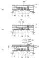
図1の左側の図は、調査に使用されたサンプルのTEM (Transmission Electron Microscope)断面像である。 The figure on the left side of FIG. 1 is a TEM (Transmission Electron Microscope) cross-sectional image of the sample used for the investigation.
このサンプルは、酸化シリコン(SiO2)膜よりなる下地絶縁膜100の上にスタック型のキャパシタQを形成してなり、同図ではそのキャパシタQの側面が拡大されている。キャパシタQは、窒化チタンアルミニウム(TiAlN)膜よりなる導電性酸素バリア膜101、イリジウム膜よりなる下部電極102、PZTよりなるキャパシタ誘電体膜103を有する。
In this sample, a stack type capacitor Q is formed on a base
また、このキャパシタQの上部電極104としては、酸化イリジウム膜よりなる導電性酸化金属膜104aと、イリジウム膜よりなる導電性向上膜104bとの二層構造を採用した。
As the
酸化イリジウムよりなる導電性酸化金属膜104aは、膜中の酸素の作用により、キャパシタ誘電体膜103を還元して劣化させ得る水素が外部からキャパシタQに入るのをブロックするように機能する。
The conductive
また、導電性向上膜104bは、上部電極104の上に形成される導電性プラグ(不図示)との間のコンタクト抵抗を下げる機能とを有する。
In addition, the
更に、水素透過防止能力に優れたアルミナよりなるキャパシタ保護絶縁膜106でこのキャパシタQを覆うと共に、キャパシタ保護絶縁膜106の上に酸化シリコンよりなる層間絶縁膜107を形成した。
Furthermore, the capacitor Q was covered with a capacitor protective
そして、この例では、下部電極102、キャパシタ誘電体膜103、及び上部電極104を一括エッチングして形成した。このような一括エッチングにより形成されるキャパシタQは、スタック型のキャパシタとも呼ばれ、占有面積が小さく高集積化に有利である。
In this example, the
なお、量産工程で採用されているキャパシタQの形成方法としては、このような一括エッチングの他に、下部電極102、キャパシタ誘電体膜103、及び上部電極104を別々にパターニングしてこれらをひな壇状にする方法もある(例えば、特許文献5の図2〜図12を参照)。このようなひな壇状のキャパシタはプレーナ型のキャパシタとも呼ばれる。
As a method for forming the capacitor Q employed in the mass production process, in addition to such collective etching, the
ここで、本願発明者が行った調査によると、上記のような一括エッチングで形成されたスタック型のキャパシタQでは、下部電極102と上部電極104との間のリーク電流が2〜3桁程度も大きくなった。
Here, according to the investigation conducted by the present inventor, in the stack type capacitor Q formed by batch etching as described above, the leakage current between the
本願発明者は、キャパシタQにおいてリーク電流が増大する理由を探るため上記のTEM像を詳しく観察したところ、キャパシタ誘電体膜103の側面に白い粒が多数存在しているのを発見した。
The inventor of the present application observed the above TEM image in detail to find out the reason why the leakage current increases in the capacitor Q, and found that a large number of white particles exist on the side surface of the capacitor
そして、この白い粒をEDX (Energy Dispersive X-ray Fluorescence Spectrometer)で調べたところ、図1の右上に示すグラフが得られた。 And when this white grain was investigated by EDX (Energy Dispersive X-ray Fluorescence Spectrometer), the graph shown in the upper right of FIG. 1 was obtained.
このグラフに示されるように、イリジウムの存在を示すピークが多数現れた。 As shown in this graph, many peaks indicating the presence of iridium appeared.
比較のために、白い粒の無い所をEDXで調べたところ、図1の右下のようなグラフが得られ、白い粒が無い所ではイリジウムが存在しないことが分かった。 For comparison, when a place without white grains was examined by EDX, a graph as shown in the lower right of FIG. 1 was obtained, and it was found that iridium was not present in places without white grains.
この結果より、白い粒はイリジウム粒であることが確認できた。 From this result, it was confirmed that the white grains were iridium grains.
このイリジウム粒は、一括エッチングによりキャパシタQを形成する際に、イリジウム膜よりなる下部電極102の側面がエッチング雰囲気に曝され、該側面から飛散したものであると考えられる。
These iridium grains are considered to be those that the side surface of the
そのイリジウム粒はキャパシタQのリークパスを形成するので、イリジウム粒を低減するのがリーク電流を低減するのに有効であると考えられる。 Since the iridium grains form a leakage path of the capacitor Q, it is considered that reducing the iridium grains is effective in reducing the leakage current.
但し、イリジウムは他の白金族元素と比較してウエットエッチングが困難なので、ウエットエッチングに頼らずにイリジウム粒を除去する必要がある。 However, since iridium is difficult to wet-etch compared to other platinum group elements, it is necessary to remove iridium grains without relying on wet etching.
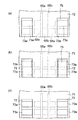
なお、本願発明者は、上記のサンプルにおいて、導電性酸素バリア膜101の側面に付着している白い粒についてもEDXで調べた。
In addition, in the above sample, the inventor of the present application also examined white particles adhering to the side surface of the conductive
その結果を図2に示す。 The result is shown in FIG.
図2の右上のグラフは、導電性酸素バリア膜101の側面付近の白い粒をEDXで調査して得られたものである。一方、右下のグラフは、白い粒の無いところを調査して得られたものである。
The upper right graph in FIG. 2 is obtained by examining white grains near the side surface of the conductive
これらの二つのグラフを比較すれば明らかなように、白い粒がある所ではイリジウムのピークが現れるのに対し、白い粒が無いところではイリジウムのピークが無く、白い粒がイリジウム粒であることが分かる。 As is clear from the comparison of these two graphs, the iridium peak appears where there are white grains, whereas there is no iridium peak where there are no white grains, and the white grains are iridium grains. I understand.
本願発明者は、このような調査結果に基づき、以下のような本発明の実施形態に想到した。 The inventor of the present application has arrived at the following embodiments of the present invention based on such investigation results.
(2)第1実施形態
図3〜図12は、本実施形態に係る半導体装置の製造途中の断面図である。
(2) First Embodiment FIGS. 3 to 12 are cross-sectional views of the semiconductor device according to the present embodiment during its manufacture.
この半導体装置は、微細化に有利なスタック型のFeRAMであり、以下のようにして作成される。 This semiconductor device is a stack type FeRAM advantageous for miniaturization, and is manufactured as follows.
最初に、図3(a)に示す断面構造を得るまでの工程について説明する。 First, steps required until a sectional structure shown in FIG.
まず、n型又はp型のシリコン(半導体)基板1表面に、トランジスタの活性領域を画定するSTI(Shallow Trench Isolation)用の溝を形成し、その中に酸化シリコン等の絶縁膜を埋め込んで素子分離絶縁膜2とする。なお、素子分離構造はSTIに限られず、LOCOS(Local Oxidation of Silicon)法で素子分離絶縁膜2を形成してもよい。
First, an STI (Shallow Trench Isolation) trench defining an active region of a transistor is formed on the surface of an n-type or p-type silicon (semiconductor)
次いで、シリコン基板1の活性領域にp型不純物を導入してpウェル3を形成した後、その活性領域の表面を熱酸化することにより、ゲート絶縁膜4となる熱酸化膜を形成する。
Next, a p-type impurity is introduced into the active region of the
続いて、シリコン基板1の上側全面に非晶質又は多結晶のシリコン膜を形成し、これらの膜をフォトリソグラフィによりパターニングして二つのゲート電極5を形成する。
Subsequently, an amorphous or polycrystalline silicon film is formed on the entire upper surface of the
pウェル3上には、上記の2つのゲート電極5が間隔をおいて平行に配置され、それらのゲート電極5はワード線の一部を構成する。
On the p-well 3, the two
次いで、ゲート電極5をマスクにするイオン注入により、ゲート電極5の横のシリコン基板1にn型不純物を導入し、第1、第2ソース/ドレインエクステンション6a、6bを形成する。
Next, n-type impurities are introduced into the
その後に、シリコン基板1の上側全面に絶縁膜を形成し、その絶縁膜をエッチバックしてゲート電極5の横に絶縁性サイドウォール7を形成する。その絶縁膜として、例えばCVD法により酸化シリコン膜を形成する。
Thereafter, an insulating film is formed on the entire upper surface of the
続いて、絶縁性サイドウォール7とゲート電極5をマスクにしながら、シリコン基板1にn型不純物を再びイオン注入することにより、二つのゲート電極5の側方のシリコン基板1の表層に、互いに間隔がおかれた第1、第2ソース/ドレイン領域(第1、第2不純物拡散領域)8a、8bを形成する。
Subsequently, n-type impurities are ion-implanted again into the
ここまでの工程により、シリコン基板1の活性領域には、ゲート絶縁膜4、ゲート電極5、及び第1、第2ソース/ドレイン領域8a、8bによって構成される第1、第2MOSトランジスタTR1、TR2が形成されたことになる。
Through the steps so far, the active region of the
次に、シリコン基板1の上側全面に、スパッタ法によりコバルト層等の高融点金属層を形成した後、この高融点金属層を加熱してシリコンと反応させ、シリコン基板1上に高融点金属シリサイド層9を形成する。その高融点金属シリサイド層9はゲート電極5の表層部分にも形成され、それによりゲート電極5が低抵抗化されることになる。
Next, after forming a refractory metal layer such as a cobalt layer on the entire upper surface of the
その後、素子分離絶縁膜2の上等で未反応となっている高融点金属層をウエットエッチングして除去する。
Thereafter, the unreacted refractory metal layer on the element
続いて、プラズマCVD法により、シリコン基板1の上側全面に窒化シリコン(SiN)膜を厚さ約200nmに形成し、それをカバー絶縁膜10とする。次いで、このカバー絶縁膜10の上に、TEOSガスを使用するプラズマCVD法により第1層間絶縁膜11として酸化シリコン膜を厚さ約1000nmに形成する。
Subsequently, a silicon nitride (SiN) film having a thickness of about 200 nm is formed on the entire upper surface of the
次いで、第1層間絶縁膜11の上面をCMP (Chemical Mechanical Polishing)法により研磨して平坦化する。このCMPの結果、第1層間絶縁膜11の厚さは、シリコン基板1の平坦面上で約700nmとなる。
Next, the upper surface of the first
そして、フォトリソグラフィによりカバー絶縁膜10と第1層間絶縁膜11とをパターニングして第1、第2ソース/ドレイン領域8a、8bの上に直径が0.25μmのコンタクトホールを形成する。更に、このコンタクトホール内にグルー膜(密着膜)とタングステン膜とを順に形成した後、第1層間絶縁膜11上の余分なグルー膜とタングステン膜とをCMP法により研磨して除去し、これらの膜をコンタクトホール内にのみ第1、第2導電性プラグ32a、32bとして残す。
Then, the
これらの第1、第2導電性プラグ32a、32bは、それぞれ第1、第2ソース/ドレイン領域8a、8bと電気的に接続される。
These first and second
なお、上記のグルー膜は、厚さ約30nmのチタン膜と厚さ約20nmの窒化チタン膜とをこの順に形成してなる。また、CMP前のタングステン膜は、第1層間絶縁膜11上で約300nmの厚さを有する。
The glue film is formed by forming a titanium film having a thickness of about 30 nm and a titanium nitride film having a thickness of about 20 nm in this order. The tungsten film before CMP has a thickness of about 300 nm on the first
ここで、第1、第2導電性プラグ32a、32bは、酸化され易いタングステンを主にして構成され、プロセス中で酸化されるとコンタクト不良を起こす恐れがある。
Here, the first and second
そこで、各導電性プラグ32a、32bの酸化を防ぐ酸化防止絶縁膜14として、これらのプラグ32a、32bと第1層間絶縁膜11の上にプラズマCVD法により酸窒化シリコン(SiON)膜を厚さ約200nmに形成する。
Therefore, a silicon oxynitride (SiON) film is formed on the
なお、酸窒化シリコン膜に代えて、窒化シリコン(SiN)膜やアルミナ膜を酸化防止絶縁膜14として形成してもよい。
Note that instead of the silicon oxynitride film, a silicon nitride (SiN) film or an alumina film may be formed as the
その後に、TEOSガスを使用するプラズマCVD法により、酸化防止絶縁膜14の上に酸化シリコン膜を厚さ約300nmに形成し、この酸化シリコン膜を下地絶縁膜15とする。
Thereafter, a silicon oxide film having a thickness of about 300 nm is formed on the oxidation-preventing insulating
次に、図3(b)に示す断面構造を得るまでの工程について説明する。 Next, steps required until a sectional structure shown in FIG.
まず、下地絶縁膜15と酸化防止絶縁膜14とをパターニングすることにより、第1導電性プラグ32aの上方のこれらの絶縁膜に第1ホール15aを形成する。
First, by patterning the
次いで、この第1ホール15a内と下地絶縁膜15の上にスパッタ法によりグルー膜35として窒化チタン膜を形成する。
Next, a titanium nitride film is formed as a
更に、CVD法を用いて、このグルー膜35の上にプラグ用導電膜36としてタングステン膜を形成し、このプラグ用導電膜36で第1ホール15aを完全に埋め込む。
Further, a tungsten film is formed as a plug
続いて、図3(c)に示すように、下地絶縁膜15の上の余分なグルー膜35とプラグ用導電膜36とをCMP法により研磨して除去する。これにより、グルー膜35とプラグ用導電膜36は、第1導電性プラグ32aと電気的に接続された第3導電性プラグ36aとして第1ホール15a内に残される。
Subsequently, as shown in FIG. 3C, the
このCMPでは、研磨対象であるグルー膜35とプラグ用導電膜36の研磨速度が下地絶縁膜15よりも速くなるようなスラリ、例えばCabot Microelectronics Corporation製のW2000を使用する。そして、下地絶縁膜15上に研磨残を残さないために、このCMPの研磨量は各膜35、36の合計膜厚よりも厚く設定され、このCMPはオーバー研磨となる。
In this CMP, a slurry in which the polishing rate of the
次に、図4(a)に示すように、酸化シリコンよりなる下地絶縁膜15を窒素含有プラズマ、例えばアンモニア(NH3)プラズマに曝し、下地絶縁膜15の表面の酸素原子にNH基を結合させる。
Next, as shown in FIG. 4A, the
このアンモニアプラズマ処理では、例えば、シリコン基板1に対して約9mm(350mils)だけ離れた位置に対向電極を有する平行平板型のプラズマ処理装置が使用される。そして、266Pa(2Torr)の圧力下において基板温度を400℃に保持しながら、チャンバ内にアンモニアガスを350sccmの流量で供給し、シリコン基板1側に13.56MHzの高周波電力を100Wのパワーで、また上記の対向電極に350kHzの高周波電力を55Wのパワーで60秒間供給することにより処理が行われる。
In this ammonia plasma processing, for example, a parallel plate type plasma processing apparatus having a counter electrode at a position separated from the
続いて、図4(b)に示すように、下地絶縁膜15と第3導電性プラグ36aのそれぞれの上にチタン膜を厚さ約20nmに形成し、このチタン膜を結晶性導電膜21とする。
Subsequently, as shown in FIG. 4B, a titanium film is formed to a thickness of about 20 nm on each of the
この結晶性導電膜21の成膜条件は特に限定されないが、本実施形態では、シリコン基板1とチタンターゲットとの距離が60mmに設定されたスパッタチャンバを用いて、0.15Paのアルゴン雰囲気中で基板温度を20℃にする。そして、2.6kWのDC電力をチャンバに5秒間供給することにより、チタンよりなる上記の結晶性導電膜21を形成する。
The film forming conditions of the crystalline
ここで、アンモニアプラズマ処理(図4(a)参照)を予め行い、下地絶縁膜15の表面の酸素原子にNH基を結合させておいたので、下地絶縁膜15上に堆積したチタン原子は下地絶縁膜15表面の酸素原子に捕獲され難くい。そのため、チタン原子が下地絶縁膜15の表面を自在に移動できるようになり、(002)方向に強く自己組織化したチタンよりなる結晶性導電膜21を形成することが可能となる。
Here, ammonia plasma treatment (see FIG. 4A) is performed in advance, and NH groups are bonded to oxygen atoms on the surface of the
なお、結晶性導電膜21の構成材料はチタンに限定されない。チタン、プラチナ、イリジウム、レニウム、ルテニウム、パラジウム、及びオスミウムのいずれか、或いはこれらの合金で結晶性導電膜21を構成してもよい。
The constituent material of the crystalline
その後に、結晶性導電膜21に対し、窒素雰囲気中において基板温度を650℃、処理時間を60秒とするRTA(Rapid Thermal Anneal)を行う。これにより、チタンよりなる結晶性導電膜21が窒化され、(111)方向に配向した窒化チタンで結晶性導電膜21が構成されることになる。
Thereafter, RTA (Rapid Thermal Anneal) is performed on the crystalline
次に、図4(c)に示すように、この結晶性導電膜21の上に導電性酸素バリア膜22として窒化チタンアルミニウム(TiAlN)膜を反応性スパッタ法で100nmの厚さに形成する。
Next, as shown in FIG. 4C, a titanium aluminum nitride (TiAlN) film is formed as a conductive
窒化チタンアルミニウムよりなる導電性酸素バリア膜22は、酸素透過防止機能に優れており、その下の第3導電性プラグ36aが酸化してコンタクト不良が発生するのを防止する役割を担う。
The conductive
この導電性酸素バリア膜22の成膜条件は特に限定されないが、本実施形態では、チタンとアルミニウムとの合金ターゲットを使用し、アルゴンガスと窒素ガスとの混合ガスをスパッタガスとして用いる。そして、アルゴンガスと窒素ガスのそれぞれの流量を40sccm、100sccmにし、253.3Paの圧力下、400℃の基板温度、そして1.0kWのスパッタパワーで導電性酸素バリア膜22を形成する。
The deposition conditions for the conductive
また、導電性酸素バリア膜22は窒化チタンアルミニウム膜に限定されない。導電性酸素バリア膜22としては、イリジウム膜又はルテニウム膜も形成し得る。
Further, the conductive
次に、図5(a)に示すように、導電性酸素バリア膜22の上に、スパッタ法により第1導電膜の下側導電層23bとしてプラチナ膜を60nmの厚さに形成する。そのプラチナ膜は、例えば、圧力が0.2Paのアルゴン雰囲気中で基板温度を400℃にし、スパッタパワーを0.5kWにして形成される。
Next, as shown in FIG. 5A, a platinum film having a thickness of 60 nm is formed on the conductive
なお、この下側導電層23bの構成材料は、イリジウム以外の貴金属であれば特に限定されず、ロジウムやパラジウムで下側導電層23bを構成するようにしてもよい。
The constituent material of the lower
次いで、図5(b)に示すように、下側導電層23bの上にイリジウム膜を厚さ40nmに形成し、そのイリジウム膜を第1導電膜の上側導電層23cとする。このイリジウム膜の成膜条件は特に限定されないが、本実施形態では、圧力が0.11Paのアルゴン雰囲気中で基板温度を500℃にし、スパッタパワーを0.3kWにする条件が採用される。
Next, as shown in FIG. 5B, an iridium film is formed to a thickness of 40 nm on the lower
更に、上側導電層23cを構成する導電性材料はイリジウムに限定されず、ルテニウム、酸化イリジウム、酸化ルテニウム、及びSrRuO3のいずれかであってもよい。
Furthermore, the conductive material constituting the upper
これにより、下側導電層23bと上側導電層23cとで構成される第1導電膜23が形成されたことになる。
Thus, the first
その第1導電膜23の結晶性はその上に後で形成される強誘電体膜の配向に大きな影響を与える。そのため、上記の下側導電層23bと上側導電層23cのそれぞれの成膜温度をなるべく高めることで、第1導電膜23の結晶性を向上させ、強誘電体膜の配向を高めるようにするのが好ましい。
The crystallinity of the first
但し、成膜温度が高すぎると、下側導電層23bと上側導電層23cのそれぞれのストレスが高くなり、各層23b、23cが膜剥がれを起こす恐れがある。
However, if the film forming temperature is too high, the stress of each of the lower
そのため、各層23b、23cを成膜する際の基板温度としては、なるべく高い温度で、且つ、ストレスが小さくなる温度を採用するのが好ましい。
Therefore, it is preferable to employ a temperature that is as high as possible and that reduces stress as the substrate temperature for forming the
下側導電層23bとしてプラチナ膜を形成する場合、下側導電層23bのストレスが小さくなる温度範囲は280℃〜300℃である。従って、この温度範囲を含み、且つ上限が高温側にシフトした250℃以上450℃以下の基板温度で下側導電層23bを形成するのが好ましい。
When a platinum film is formed as the lower
一方、上側導電層23cとしてイリジウム膜を形成する場合、上側導電層23cのストレスが小さくなる温度範囲は420℃〜450℃である。よって、この温度範囲を含み、且つ上限が高温側にシフトした400℃以上550℃以下の基板温度で上側導電層23cを形成するのが好ましい。
On the other hand, when an iridium film is formed as the upper
このような温度範囲を採用することで、各層23b、23cの膜剥がれを防止しつつ、第1導電膜23の結晶性を高めることが可能となる。
By adopting such a temperature range, it is possible to improve the crystallinity of the first
ここで、既述のように、結晶性導電膜21を構成する窒化チタン膜が(111)方向に配向しているため、この配向の作用によっても第1導電膜23の結晶性は良好になる。
Here, as described above, since the titanium nitride film constituting the crystalline
その後に、アルゴン雰囲気中で基板温度を650℃以上とするRTAを第1導電膜23に対して60秒間行うことにより、各膜21〜23同士の密着性を高めると共に、第1導電膜23の結晶性を改善する。
Thereafter, by performing RTA with the substrate temperature of 650 ° C. or higher in an argon atmosphere for 60 seconds on the first
このRTAの雰囲気は、不活性ガスの雰囲気であれば特に限定されない。そのような不活性ガスとしては、アルゴンガスの他に、窒素ガスや二酸化窒素(N2O)ガスもある。 The atmosphere of this RTA is not particularly limited as long as it is an inert gas atmosphere. Examples of such inert gas include nitrogen gas and nitrogen dioxide (N 2 O) gas in addition to argon gas.
続いて、図5(c)に示すように、MOCVD法により第1導電膜23の上にペロブスカイト構造のPZT (Lead Zirconate Titanate: PbZrTiO3)膜を形成し、このPZT膜を第1強誘電体膜24bとする。MOCVD法で形成された第1強誘電体膜24bは、成膜の時点で既に結晶化しているため、第1強誘電体膜24bを結晶化させるための結晶化アニールは不要である。
Subsequently, as shown in FIG. 5C, a PZT (Lead Zirconate Titanate: PbZrTiO 3 ) film having a perovskite structure is formed on the first
そのMOCVD法は次のようにして行われる。 The MOCVD method is performed as follows.
まず、Pb(DPM)2(化学式Pb(C11H19O2)2))、Zr(dmhd)4(化学式Zr(C9H15O2)4)、及びTi(O−iOr)2(DPM)2(化学式Ti(C3H7O)2(C11H19O2)2)のそれぞれをTHF(Tetra Hydro Furan: C4H8O)溶媒中にいずれも0.3mol/lの濃度で溶解し、Pb、Zr、及びTiの各液体原料を作成する。次いで、これらの液体原料をMOCVD装置の気化器にそれぞれ0.326ml/分、0.200ml/分、および0.200ml/分の流量で供給して気化させることにより、Pb、Zr、及びTiの原料ガスを得る。なお、上記の気化器には、各液体原料と共に、流量が0.474ml/分のTHF溶媒も供給される。 First, Pb (DPM) 2 (chemical formula Pb (C 11 H 19 O 2 ) 2 )), Zr (dmhd) 4 (chemical formula Zr (C 9 H 15 O 2 ) 4 ), and Ti (O-iOr) 2 ( Each of DPM) 2 (chemical formula Ti (C 3 H 7 O) 2 (C 11 H 19 O 2 ) 2 ) is 0.3 mol / l in THF (Tetra Hydro Furan: C 4 H 8 O) solvent. Dissolve at a concentration to create Pb, Zr, and Ti liquid raw materials. Next, these liquid raw materials are supplied to the vaporizer of the MOCVD apparatus at a flow rate of 0.326 ml / min, 0.200 ml / min, and 0.200 ml / min, respectively, to vaporize them, so that Pb, Zr, and Ti are vaporized. A raw material gas is obtained. The vaporizer is supplied with a THF solvent having a flow rate of 0.474 ml / min together with each liquid raw material.
更に、上記の原料ガスをチャンバに供給しながら、チャンバ内の圧力を665Pa(5Torr)にし、基板温度を620℃に維持する。そして、このような状態を620秒間維持することにより、上記したPZT膜が100nmの厚さに形成される。 Further, while supplying the source gas to the chamber, the pressure in the chamber is set to 665 Pa (5 Torr), and the substrate temperature is maintained at 620 ° C. Then, by maintaining such a state for 620 seconds, the PZT film described above is formed to a thickness of 100 nm.
なお、第1強誘電体膜24bはPZT膜に限定されない。ランタン、カルシウム、ストロンチウム、及びシリコンの少なくとも一つをPZTにドープした材料で第1強誘電体膜24bを構成してもよい。これらの材料はペロプスカイト構造を有するので、その下の上側導電層23cをペロプスカイト構造のSrRuO3で構成すると、上側導電層23cと第1強誘電体膜24bとの格子マッチングが良好となり、第1強誘電体膜24bの結晶性が高められる。
The first
なお、(Bi1-xRx)Ti3O12(Rは希土類元素で0<x<1)、SrBi2Ta2O9、及びSrBi4Ti4O15等のBi層状構造化合物で第1強誘電体膜24bを構成してもよい。
In addition, (Bi 1-x R x ) Ti 3 O 12 (R is a
更に、強誘電体材料に代えて、ジルコニウムや鉛を含む金属酸化物高誘電体材料で第1強誘電体膜24bを形成してもよい。
Furthermore, instead of the ferroelectric material, the first
ここで、既述のように、(111)方向に配向した窒化チタンよりなる結晶性導電膜21の作用により第1導電膜23の結晶性は良好である。そのため、第1導電膜23の上に形成される第1強誘電体膜24bの結晶性も良好となり、第1強誘電体膜24bの強誘電体特性、例えば残留分極電荷量等が高められる。
Here, as described above, the crystallinity of the first
次に、第1強誘電体膜24bの上に第2強誘電体膜24cとしてスパッタ法でPZT膜を1〜30nmの厚さ、例えば20nmに形成し、これら第1、第2強誘電体膜24b、24cを強誘電体膜24とする。
Next, a PZT film having a thickness of 1 to 30 nm, for example, 20 nm, is formed as a second
なお、MOCVD法で形成された第1強誘電体膜24bと異なり、スパッタ法で形成された第2強誘電体膜24cは、成膜の時点で結晶化しておらず、アモルファス状態となっている。
Unlike the first
また、第2強誘電体膜24cはPZTに限定されない。
The second
PZTのようにABO3型ペロブスカイト構造(A=Bi、Pb、Ba、Sr、Ca、Na、K、及び希土類元素のいずれか一つ、B=Ti、Zr、Nb、Ta、W、Mn、Fe、Co、及びCrのいずれか一つ)を有する強誘電体材料で第2強誘電体膜24cを構成してもよい。
ABO 3- type perovskite structure like PZT (A = Bi, Pb, Ba, Sr, Ca, Na, K and any one of rare earth elements, B = Ti, Zr, Nb, Ta, W, Mn, Fe , Co, and Cr) may be used to form the second
更に、ランタン、カルシウム、ストロンチウム、及びシリコンの少なくとも一つをPZTにドープした材料で第2強誘電体膜24cを構成してもよい。これらの元素をPZT膜にドープすることで、第2強誘電体膜24cの疲労損失とインプリント特性が改善されると共に、キャパシタへの書き込み電圧や読み出し電圧を低くすることができる。
Furthermore, the second
また、(Bi1-xRx)Ti3O12(Rは希土類元素で0<x<1)、SrBi2Ta2O9、及びSrBi4Ti4O15等のBi層状構造化合物で第2強誘電体膜24cを構成してもよい。
In addition, (Bi 1-x R x ) Ti 3 O 12 (R is a
また、第2強誘電体膜24cの成膜方法もスパッタ法に限定されない。ゾル・ゲル法やMOCVD法で第2強誘電体膜24cを形成してもよい。MOCVD法を採用する場合、その成膜条件としては、第1強誘電体膜24bと同様の条件が採用され得る。
Further, the film formation method of the second
但し、後述の理由により、第2強誘電体膜24cはアモルファス状態又は微結晶からなる膜であるのが好ましく、アモルファスな第2強誘電体膜24cを成膜できるスパッタ法を採用するのが最も好ましい。
However, for the reason described later, the second
続いて、図6(a)に示すように、シリコン基板1を加熱しながら強誘電体膜24の上に第1導電性酸化金属膜25dとして反応性スパッタ法で酸化イリジウム(IrOx)膜を厚さ約50nmに形成する。なお、このようにシリコン基板1を加熱するスパッタ法で形成された酸化イリジウム膜は、結晶化のためのプロセスを行わなくても、成膜の時点で既に結晶化している。
Subsequently, as shown in FIG. 6A, an iridium oxide (IrO x ) film is formed as a first conductive
その第1導電性酸化金属膜25dの成膜条件は特に限定されない。本実施形態では、基板温度を300℃にすると共に、流量が140sccmのアルゴンガスと、流量が10〜90sccm、例えば60sccmの酸素ガスとの混合ガスをスパッタガスとして用い、更にスパッタパワーを1kW〜2kWとする。
The film forming conditions for the first conductive
ここで、上記した酸化イリジウムのスパッタでは、イリジウムターゲットから飛来したイリジウム原子がスパッタ雰囲気中で酸化されることで基板上に酸化イリジウムが堆積する。そのため、堆積した酸化イリジウムの中には、雰囲気中における酸化が不十分なものも含まれ、酸化イリジウム膜全体としては化学量論組成(IrO2)よりも酸素が少ない状態になり易い。 Here, in the above-described sputtering of iridium oxide, iridium atoms flying from the iridium target are oxidized in the sputtering atmosphere, so that iridium oxide is deposited on the substrate. Therefore, some of the deposited iridium oxide is insufficiently oxidized in the atmosphere, and the iridium oxide film as a whole is likely to be in a state of less oxygen than the stoichiometric composition (IrO 2 ).
そのため、化学量論的組成の酸化イリジウムの化学式をIrOx1と書くとx1は2であるのに対し、上記の条件で従って形成された第1導電性酸化金属膜25dでは、酸化イリジウムの化学式をIrOx2と書くとx2が1.3〜1.9程度の値となり、比x2/x1は1よりかなり小さくなる。
Therefore, when the chemical formula of iridium oxide having a stoichiometric composition is written as IrO x1 , x1 is 2, whereas in the first conductive
ここで、第1強誘電体膜24bは、第2強誘電体膜24cや第1導電性酸化金属膜25dをスパッタ法で形成した際にスパッタガスによってダメージを受けていると共に、膜中の酸素濃度が欠乏し、その強誘電体特性が劣化している恐れがある。
Here, the first
そこで、上記の第1導電性酸化金属膜25dを形成した後に、酸化性ガス含有雰囲気中、例えばアルゴンと酸素との混合雰囲気中でRTAを行うことにより、スパッタにより受けた第1強誘電体膜24bのダメージを回復させると共に、第1強誘電体膜24bの酸素欠損を補償する。
Therefore, after the first conductive
このRTAの条件は特に限定されないが、基板温度は650℃以上、より好ましくは700℃〜750℃とするのが好ましい。本実施形態では、基板温度を725℃とする。また、アルゴンと酸素の流量をそれぞれ2000sccm、20sccmとし、処理時間を60秒とする。 The RTA conditions are not particularly limited, but the substrate temperature is preferably 650 ° C. or higher, more preferably 700 ° C. to 750 ° C. In this embodiment, the substrate temperature is 725 ° C. The flow rates of argon and oxygen are 2000 sccm and 20 sccm, respectively, and the processing time is 60 seconds.
なお、このRTAの雰囲気は、不活性ガスと酸化性ガスとの混合雰囲気であれば特に限定されない。このうち、不活性ガスとしては、アルゴン、窒素(N2)、及び二酸化窒素のいずれかを採用し得る。 The atmosphere of RTA is not particularly limited as long as it is a mixed atmosphere of an inert gas and an oxidizing gas. Among these, any of argon, nitrogen (N 2 ), and nitrogen dioxide can be adopted as the inert gas.
更に、第2強誘電体膜24cをアモルファスに形成したので、このRTAによって第1導電性酸化金属膜25dから強誘電体膜24に拡散するイリジウム原子は、第2強誘電体膜24c中に留まるようになり、第1強誘電体膜24bに至り難くなる。その結果、結晶化して優れた強誘電体特性を呈する第1強誘電体膜24の粒界にイリジウムが拡散し難くなるため、そのイリジウムによってリークパスが形成されるのが抑制され、強誘電体キャパシタのリーク電流を効果的に防止することが可能となる。
Furthermore, since the second
このような利点は、微結晶からなる膜で第2強誘電体膜24cを構成しても得られる。
Such an advantage can be obtained even if the second
上記のようにして第1導電性酸化金属膜25dを形成した後は、基板温度を室温とする反応性スパッタ法を用いて、第1導電性酸化金属膜25dの上に第2導電性酸化金属膜25eとして酸化イリジウム膜を厚さ約100〜300nm、例えば200nmに形成する。その第2導電性酸化金属膜25eは、圧力が0.8Paのスパッタ雰囲気中、スパッタパワーを1.0kWにし、成膜時間を79秒とすることで形成される。
After the first conductive
ここで、高い成膜温度で結晶化された第1導電性酸化金属膜25dとは異なり、基板温度を室温とするスパッタ法で形成された第2導電性酸化金属膜25eはアモルファス状態になる。
Here, unlike the first conductive
ところで、第2導電性酸化金属膜25eにおいて酸素が不足すると、第2導電性酸化金属膜25eの触媒作用が高まるため、外部の水分が第2導電性酸化金属膜25eに触れて水素が発生するようになる。水素は、強誘電体膜24を還元してその強誘電体特性を劣化させるという問題があるため、FeRAMの製造工程では水素の発生を極力抑える必要がある。
By the way, when oxygen is insufficient in the second conductive
従って、水素の発生を防止するという観点からすると、第2導電性酸化金属膜25eを構成するイリジウムの酸化数は、第1導電性酸化金属膜25dのそれよりも大きいのが好ましい。
Therefore, from the viewpoint of preventing hydrogen generation, the oxidation number of iridium constituting the second conductive
そこで、本実施形態では、第2導電性酸化金属膜25eを形成するときに、スパッタガスに占める酸素の流量比を、第1導電性酸化金属膜25dを形成する工程におけるよりも多くすることで、酸化イリジウムの組成を化学量論組成(IrO2)に近づけ、第2導電性酸化金属膜24eの触媒作用を抑えるようにする。このときのスパッタガスの流量は、例えばアルゴンが100sccm、酸素が100sccmとされる。
Therefore, in the present embodiment, when the second conductive
第2導電性酸化金属膜24eを構成する酸化イリジウムの化学式をIrOy2と書くと、上記の条件に従った場合y2は略2になる。化学量論的組成の酸化イリジウムの化学式をIrOy1と書くとy1は2であるため、比y2/y1は1に近い値となり、第1導電性酸化金属膜25dの比x2/x1との大小関係はy2/y1>x2/x1となる。
When the chemical formula of iridium oxide constituting the second conductive metal oxide film 24e is written as IrO y2 , y2 becomes approximately 2 in accordance with the above conditions. When the chemical formula of iridium oxide having a stoichiometric composition is written as IrO y1 , y1 is 2, so the ratio y2 / y1 is close to 1, and the magnitude of the ratio x2 / x1 of the first conductive
このような第2導電性酸化金属膜25eと第1導電性酸化金属膜25dにより、図示のような導電性酸化金属膜25bが構成される。
The second conductive
その第1導電性酸化金属膜25dは、膜中の酸素の作用により水素をブロックする機能を有し、水素からキャパシタ誘電体膜24を保護する役割も担う。
The first conductive
なお、第1、第2導電性酸化金属膜25d、25eの構成材料は酸化イリジウムに限定されない。
The constituent materials of the first and second conductive
但し、第1強誘電体膜24bをMOCVD法で形成する場合は、第1、第2導電性酸化金属膜25d、25eとしてプラチナの酸化膜を採用すると、強誘電体膜24を構成するPZTの鉛とプラチナとが反応するため、強誘電体膜24の強誘電体特性が劣化し、強誘電体膜24の残留分極電荷量が低減してしまう。よって、この場合は、第1、第2導電性酸化金属膜25d、25eの構成材料として、イリジウム(Ir)、ルテニウム(Ru)、ロジウム(Rh)、レニウム(Re)、オスミウム(Os)、及びパラジウム(Pd)のいずれかの酸化物を採用するのが好ましい。
However, when the first
但し、上記したPZTの鉛とプラチナとの反応が問題にならないなら、第1、第2導電性酸化金属膜25d、25eとしてプラチナの酸化膜を採用してもよい。
However, if the reaction between PZT lead and platinum does not matter, platinum oxide films may be employed as the first and second conductive
また、上記したように、第2導電性酸化金属膜25eでの水素の発生を防止するために、第2導電性酸化金属膜25eを構成する金属酸化物は、第1導電性酸化金属膜25dのそれよりも多く酸化されているのが好ましい。第1導電性酸化金属膜25dと第2導電性酸化金属膜25eのそれぞれを構成する金属酸化物の化学量論的な組成をAOx1、BOy1(AとBは金属元素)、成膜後のこれらの実際の組成をAOx2、BOy2と書くと、上記の条件はy2/y1>x2/x1となる。
Further, as described above, in order to prevent the generation of hydrogen in the second conductive
更に、第1、第2導電性酸化金属膜25d、25eの膜厚については、第1導電性酸化金属膜25dの方が第2導電性酸化金属膜25eよりも薄いのが好ましい。
Further, regarding the film thicknesses of the first and second conductive
これは、第1導電性酸化金属膜25dの形成後に行われる既述のRTAにおいて、第1導電性酸化金属膜25dが薄い方が強誘電体膜24の全体に酸素が行き渡り易くなり、強誘電体膜24のダメージの回復が効果的に図られるためである。更に、第2導電性酸化金属膜25eが後で形成される第2層間絶縁膜からの水分や水素等の還元性物質をブロックする役割も担っているので、その厚さが厚いほうが還元性物質に対するブロック性が高まるためでもある。
This is because, in the RTA described above after the formation of the first conductive
続いて、図6(b)に示すように、導電性酸化金属膜25bの上に、導電性向上膜25cとしてイリジウム膜をスパッタ法により厚さ50nmに形成する。そのスパッタ法は、圧力が1Paのアルゴン雰囲気中で行われ、1.0kWのスパッタパワーがスパッタ雰囲気に投入される。
Subsequently, as shown in FIG. 6B, an iridium film is formed as a
導電性向上膜25cは、その下の導電性酸化金属膜25bと共に第2導電膜25を構成し、導電性酸化金属膜25bだけでは不足しがちな第2導電膜25の導電性を補う役割を担う。更に、導電性向上膜25cは、その材料であるイリジウムが水素に対するバリア性に富むため、外部の水素をブロックして強誘電体膜24の劣化を防止する役割も担う。
The
なお、イリジウム膜に代えて、ルテニウム膜、ロジウム膜、及びパラジウム膜のいずれかを導電性向上膜25cとして形成してもよい。
Instead of the iridium film, any one of a ruthenium film, a rhodium film, and a palladium film may be formed as the
この後に、シリコン基板1の背面を洗浄する。
Thereafter, the back surface of the
次に、図7(a)に示すように、第2導電膜25の上にスパッタ法により窒化チタン膜を形成し、その窒化チタン膜を第1マスク材料層26とする。
Next, as shown in FIG. 7A, a titanium nitride film is formed on the second
更に、TEOSガスを使用するプラズマCVD法を用いて、第1マスク材料層26の上に第2マスク材料層27として酸化シリコン膜を形成する。
Further, a silicon oxide film is formed as the second
次いで、図7(b)に示すように、第2マスク材料層27を島状にパターニングすることにより第2ハードマスク27aを形成する。
Next, as shown in FIG. 7B, a second
次に、図8(a)に示す断面構造を得るまでの工程について説明する。 Next, steps required until a sectional structure shown in FIG.
まず、第2ハードマスク27aをマスクにして第1マスク材料層26をエッチングすることにより第1ハードマスク26aを形成する。
First, the first
次いで、第1、第2ハードマスク26a、27aで覆われていない領域の第2導電膜25、強誘電体膜24、及び第1導電膜23をドライエッチングし、下部電極23a、キャパシタ誘電体膜24a、及び上部電極25aで構成されるキャパシタQを形成する。
Next, the second
そのドライエッチングのガスは特に限定されないが、第1導電膜23、及び第2導電膜25に対するエッチングガスとしてはHBrと酸素との混合ガスが使用される。一方、強誘電体膜24に対するエッチングガスとしては塩素とアルゴンとの混合ガスが使用される。
The dry etching gas is not particularly limited, but a mixed gas of HBr and oxygen is used as an etching gas for the first
また、第1導電膜23用のエッチングガスに対して導電性酸素バリア膜22はエッチング耐性を有するので、キャパシタQを形成した後でも結晶性導電膜21の全面に導電性酸素バリア膜22は残存する。
Further, since the conductive
このようにして形成されたキャパシタQの下部電極23aは、導電性酸素バリア膜22、結晶性導電膜21、及び第3導電性プラグ36aを介して第1導電性プラグ32aと電気的に接続される。
The
更に、上記のように強誘電体膜24と第1導電膜23とを一括エッチングすることにより、キャパシタ誘電体膜24aと下部電極23aのそれぞれの側面は同一面内に存在することになる。
Further, the side surfaces of the
ここで、上記のエッチングによって下部電極23aとされる第1導電膜23は、プラチナよりなる下側導電層23bとイリジウムよりなる上側導電層23cとの二層構造となっているので、第1導電膜23をイリジウム膜のみの単層構造にする場合と比較して、第1導電膜23においてイリジウムが占める割合が小さい。
Here, the first
そのため、上記のキャパシタQのエッチングにおいて、下部電極23aの側面からエッチング雰囲気中に飛散するイリジウム粒が低減される。これにより、キャパシタ誘電体膜24aの側面に付着するイリジウム粒を低減することができ、そのイリジウム粒によって下部電極23aと上部電極25aとの間にリークパスが形成されるのを抑制できる。
Therefore, in the etching of the capacitor Q, iridium particles scattered from the side surface of the
イリジウム粒の飛散量を効果的に低減するには、下側導電層23bをイリジウムよりなる上側導電層23cよりも厚くすることで、下部電極23aにおいて上側導電導電層23cの占める割合を小さくするのが好ましい。例えば、下側導電層23bを上側導電層23cの1〜9倍の厚さに形成するのが好ましい。
In order to effectively reduce the amount of scattered iridium particles, the lower
続いて、図8(b)に示すように、過酸化水素(H2O2)、アンモニア、及び水の混合溶液をエッチング液として用い、酸化シリコンよりなる第2ハードマスク27aをウエットエッチングにより除去する。なお、ドライエッチングにより第2ハードマスク27aを除去してもよい。
Subsequently, as shown in FIG. 8B, the second
次に、図9(a)に示す断面構造を得るまでの工程について説明する。 Next, steps required until a sectional structure shown in FIG.
まず、第1ハードマスク26a(図8(b)参照)をマスクとして用いながら、結晶性導電膜21と導電性酸素バリア膜22とをエッチングし、これらの膜をキャパシタQの下にのみ残す。このエッチングはドライエッチングにより行われ、そのエッチングガスとしては例えばアルゴンと塩素との混合ガスが使用される。
First, while using the first
また、このエッチングガスに対し第1ハードマスク26aもエッチングされるため、エッチングの終了時には第1ハードマスク26aは除去される。
Further, since the first
続いて、図9(b)に示すように、キャパシタQを覆うアルミナ(Al2O3)膜を厚さ約20nmに形成し、そのアルミナ膜を第1キャパシタ保護絶縁膜39とする。第1キャパシタ保護絶縁膜39を構成するアルミナは、水素の透過防止能力に優れているため、外部の水素はこの第1キャパシタ保護絶縁膜39によってブロックされ、水素によるキャパシタ誘電体膜24aの劣化を防止することができる。
Subsequently, as shown in FIG. 9B, an alumina (Al 2 O 3 ) film covering the capacitor Q is formed to a thickness of about 20 nm, and the alumina film is used as a first capacitor
ここで、キャパシタ誘電体膜24aは、キャパシタQを形成する際のドライエッチング(図8(b)参照)や、スパッタ法による第1キャパシタ保護絶縁膜39の成膜によってダメージを受けている。
Here, the
そこで、このダメージからキャパシタ誘電体膜24aを回復させる目的で、図10(a)に示すように、酸素含有雰囲気中においてキャパシタ誘電体膜24aに対して回復アニールを施す。この回復アニールの条件は特に限定されないが、本実施形態では、炉内において基板温度を550℃〜700℃、例えば650℃とし、約60分間行われる。
Therefore, for the purpose of recovering the
続いて、図10(b)に示すように、第1キャパシタ保護絶縁膜39の上に、CVD法によりアルミナ膜を厚さ約20nmに形成し、このアルミナ膜を第2キャパシタ保護絶縁膜40とする。
Subsequently, as shown in FIG. 10B, an alumina film is formed to a thickness of about 20 nm on the first capacitor
次に、図11(a)に示す断面構造を得るまでの工程について説明する。 Next, steps required until a sectional structure shown in FIG.
まず、TEOSガスを反応ガスとするプラズマCVDにより、第2キャパシタ保護絶縁膜40の上に第2層間絶縁膜41として酸化シリコン膜を形成する。その反応ガスには、酸素ガスとヘリウムガスも含まれる。また、第2層間絶縁膜41の膜厚は特に限定されないが、本実施形態では、シリコン基板1の平坦面上での厚さを1500nmとする。
First, a silicon oxide film is formed as a second
なお、酸化シリコン膜に代えて、絶縁性の無機膜を第2層間絶縁膜41として形成してもよい。
Note that an insulating inorganic film may be formed as the second
その後に、CMP法により第2層間絶縁膜41の表面を研磨して平坦化する。
Thereafter, the surface of the second
更に、第2層間絶縁膜41に対する脱水処理として、第2層間絶縁膜41の表面をN2Oプラズマに曝す。このN2Oプラズマにより、第2層間絶縁膜41内に残留する水分が除去されると共に、第2層間絶縁膜41への水分の再吸収が防止される。
Further, as a dehydration process for the second
なお、この脱水処理としてN2プラズマ処理を行ってもよい。 Note that N 2 plasma treatment may be performed as the dehydration treatment.
続いて、第2層間絶縁膜41の上に、スパッタ法により平坦なアルミナ膜を厚さ約20nm〜100nmに形成し、そのアルミナ膜を第3キャパシタ保護絶縁膜42とする。この第3キャパシタ保護絶縁膜42は、平坦化された第2層間絶縁膜41上に形成されるため優れたカバレッジ特性が要求されず、上記のように安価なスパッタ法で形成される。但し、第3キャパシタ保護絶縁膜42の成膜方法はスパッタ法に限定されず、CVD法であってもよい。
Subsequently, a flat alumina film having a thickness of about 20 nm to 100 nm is formed on the second
その後に、図11(b)に示すように、TEOSガスを使用するプラズマCVD法を用いて、第3キャパシタ保護絶縁膜42の上に、キャップ絶縁膜43として酸化シリコン膜を800〜1000nm程度の厚さに形成する。なお、このキャップ絶縁膜43として、酸窒化シリコン膜又は窒化シリコン膜を形成してもよい。
After that, as shown in FIG. 11B, a silicon oxide film as a
更に、このキャップ絶縁膜43に対してCMPを行いその表面を平坦化してもよい。
Further, CMP may be performed on the
次に、図12(a)に示す断面構造を得るまでの工程について説明する。 Next, steps required until a sectional structure shown in FIG.
まず、第1〜第3キャパシタ保護絶縁膜39、40、42、第2層間絶縁膜41、キャップ絶縁膜43をパターニングすることにより、上部電極25a上のこれらの膜に導電性向上膜25c(図6(b)参照)に至る深さの第2ホール41aを形成する。
First, by patterning the first to third capacitor
次いで、ここまでの工程でキャパシタ誘電体膜24aが受けたダメージを回復させるため、不図示の炉内にシリコン基板1を入れ、酸素雰囲気中で基板温度を550℃とする回復アニールを行う。
Next, in order to recover the damage received by the
次に、第2導電性プラグ32bの上の第1〜第3キャパシタ保護絶縁膜39、40、42、第2層間絶縁膜41、キャップ絶縁膜43、下地絶縁膜15、及び酸化防止絶縁膜14をパターニングして、これらの膜に第3ホール41bを形成する。
Next, the first to third capacitor
なお、このパターニングの際、第2ホール41aは、レジストパターンで覆われており、そのレジストパターンによってエッチング雰囲気から保護されている。
In this patterning, the
ここで、もし、これらのホール41a、41bを同時に形成しようとすると、深い第3ホール41bが開口されるまで第2ホール41a内の上部電極25aが長時間にわたってエッチング雰囲気に曝され、キャパシタ誘電体膜24aが劣化するという問題が発生する。
If these
本実施形態では、上記のように深さの異なる第2、第3ホール41a、41bを別々に形成するので、このような問題を回避することができる。
In the present embodiment, since the second and
更に、第2ソース/ドレイン領域8b上の第2導電性プラグ32bは、本工程が終了するまで、酸化防止絶縁膜14によって覆われているので、第2導電性プラグ32bを構成するタングステンが酸化してコンタクト不良を起こすのが防止される。
Furthermore, since the second
続いて、キャップ絶縁膜43上と第2、第3ホール41a、41b内に、グルー膜としてスパッタ法によりチタン膜と窒化チタン膜とをこの順に形成する。
Subsequently, a titanium film and a titanium nitride film are formed in this order as a glue film on the
なお、窒化チタン膜についてはMOCVD法で形成してもよい。その場合、窒化チタン膜から炭素を除去するため、窒素と水素とをプラズマ化してなる雰囲気中で窒化チタン膜をアニールするのが好ましい。このように水素含有雰囲気中でアニールを行っても、上部電極25aの最上層に形成されたイリジウムよりなる導電性向上膜25c(図6(b)参照)が水素をブロックするので、水素によって導電性酸化金属膜25bが還元されることは無い。
Note that the titanium nitride film may be formed by the MOCVD method. In that case, in order to remove carbon from the titanium nitride film, it is preferable to anneal the titanium nitride film in an atmosphere formed by converting nitrogen and hydrogen into plasma. Even when annealing is performed in a hydrogen-containing atmosphere in this manner, the
また、グルー膜はチタン膜と窒化チタン膜との積層膜に限定されず、チタン膜、窒化チタン膜、窒化タンタル膜、及び窒化チタンアルミニウム膜のいずれかよりなる単層膜、又はこれらの積層膜でグルー膜を構成してもよい。 Further, the glue film is not limited to a laminated film of a titanium film and a titanium nitride film, and is a single layer film made of any one of a titanium film, a titanium nitride film, a tantalum nitride film, and a titanium aluminum nitride film, or a laminated film thereof. A glue film may be formed.
更に、CVD法によりグルー膜の上にタングステン膜を形成し、このタングステン膜で第2、第3ホール41a、41bを完全に埋め込む。
Further, a tungsten film is formed on the glue film by the CVD method, and the second and
そして、キャップ絶縁膜43上の不要なグルー膜とタングステン膜とをCMP法により研磨して除去し、これらの膜を第2、第3ホール41a、41b内にのみ第4、第5導電性プラグ47a、47bとして残す。
Then, unnecessary glue films and tungsten films on the
これらのプラグのうち、第4導電性プラグ47aは、キャパシタQの上部電極25aと電気的に接続される。一方、第5導電性プラグ47bは、第2導電性プラグ32bに電気的に接続され、その第2導電性プラグ32bと共にビット線の一部を構成する。
Among these plugs, the fourth
ここで、第4導電性プラグ47aのグルー膜を構成する窒化チタン膜が、上部電極25aを構成する導電性酸化金属膜25bに触れると、上部電極25aと第4導電性プラグ47aとの間のコンタクト抵抗が高くなるという不都合がある。この点に鑑み、本実施形態では、上部電極25aの最上層に、イリジウムよりなる導電性向上膜25cを形成したので、上部電極25aと第4導電性プラグ47aとの間のコンタクト抵抗を低くすることができる。
Here, when the titanium nitride film constituting the glue film of the fourth
その後に、図12(b)に示すように、キャップ絶縁膜43と各導電性プラグ47a、47bのそれぞれの上にスパッタ法で金属積層膜を形成し、この金属積層膜をパターニングして金属配線49aとビット線用の導電性パッド49bとを形成する。
Thereafter, as shown in FIG. 12B, a metal laminated film is formed on the
その金属積層膜として、厚さ60nmのチタン膜、厚さ30nmの窒化チタン膜、厚さ360nmの銅含有アルミニウム膜、厚さ5nmのチタン膜、及び厚さ70nmの窒化チタン膜をこの順に形成する。 As the metal laminated film, a titanium film having a thickness of 60 nm, a titanium nitride film having a thickness of 30 nm, a copper-containing aluminum film having a thickness of 360 nm, a titanium film having a thickness of 5 nm, and a titanium nitride film having a thickness of 70 nm are formed in this order. .
以上により、本実施形態に係る半導体装置の基本構造が完成したことになる。 As described above, the basic structure of the semiconductor device according to the present embodiment is completed.
上記した本実施形態によれば、図5(b)に示したように、キャパシタの下部電極23aとなる第1導電膜23を、プラチナよりなる下側導電層23bとイリジウムよりなる上側導電層23cとの二層構造にした。
According to the above-described embodiment, as shown in FIG. 5B, the first
これにより、第1導電膜23をイリジウム膜の単層構造にする場合と比較して、第1導電膜23においてイリジウムが占める割合が減る。そのため、第1導電膜23と強誘電体膜24とを一括エッチングする工程(図8(a))において、第1導電膜23からエッチング雰囲気中に放出されるイリジウム粒を低減することが可能となる。その結果、上記のエッチング中にキャパシタ強誘電体膜23aの側面に再付着するイリジウム粒の数を減らすことができ、そのイリジウム粒に起因してキキャパシタ誘電体膜23aの側面にリークパスが発生するのが抑えられ、高品位なキャパシタQを備えた半導体装置を提供することが可能となる。
Thereby, compared with the case where the 1st electrically
このようにイリジウム粒を減らすという観点からすれば、下側導電層23bの構成材料は、イリジウム以外の貴金属であれば特に限定されない。これは、イリジウム以外の貴金属は、エッチングされてもイリジウムのように多量に粒状に飛散せず、キャパシタのリーク電流に大きな影響を与えないからである。また、イリジウム以外の貴金属は、第2ハードマスク27aをウエットエッチングする工程(図8(b))で使用されるエッチング液によってある程度エッチングされる。そのため、粒状に飛散したイリジウム以外の貴金属は、ハードマスク27aの除去時にウエットエッチングによって溶解される。
Thus, from the viewpoint of reducing iridium grains, the constituent material of the lower
なお、イリジウム粒を低減するだけなら、イリジウム以外の貴金属よりなる単層膜、例えばプラチナ膜のみで第1導電膜23を構成することも考えられる。
If only iridium grains are reduced, it is also conceivable to form the first
しかし、第1導電膜23は、キャパシタの下部電極としての機能の他に、自身の結晶性によりその上の強誘電体膜24の結晶性を向上させる機能も必要である。イリジウム膜はこの機能に優れているので、本実施形態のように第1導電膜23を二層構造にし、その最上層の上側導電層23cにイリジウム膜を形成するのが好ましい。
However, the first
但し、最上層の上側導電層23cとしてプラチナ膜を形成すると、PZTよりなる強誘電体膜24に含まれる鉛とプラチナとの相互拡散によって強誘電体膜24の強誘電体特性、例えば残留分極電荷量が低下するという問題がある。例えば、特許文献2と特許文献3ではこのような問題が発生する。
However, when a platinum film is formed as the uppermost upper
更に、プラチナは他の貴金属にくらべて高価なので、製造コストの上昇を防ぐという観点からも、上側導電層23cとしてプラチナ膜を形成するのは好ましくない。
Furthermore, since platinum is more expensive than other precious metals, it is not preferable to form a platinum film as the upper
これらの理由により、上側導電層23cの構成材料としては、プラチナ以外の導電性材料を選択するのが好ましい。
For these reasons, it is preferable to select a conductive material other than platinum as the constituent material of the upper
このような下側導電層23bと上側導電層23cのそれぞれの材料の選択の仕方については、後述の実施形態でも同様である。
The method of selecting the respective materials for the lower
(2)第2実施形態
図13〜図18は、本発明の第2実施形態に係る半導体装置の製造途中の断面図である。なお、これらの図において第1実施形態で説明した要素には第1実施形態と同じ符号を付し、以下ではその説明を省略する。
(2) Second Embodiment FIGS. 13 to 18 are cross-sectional views in the course of manufacturing a semiconductor device according to a second embodiment of the present invention. In these drawings, the elements described in the first embodiment are denoted by the same reference numerals as those in the first embodiment, and the description thereof is omitted below.
第1実施形態の図3(c)の工程では、グルー膜35とプラグ用導電膜36とをCMP法により研磨することで第3導電性プラグ36aを形成した。
In the process of FIG. 3C of the first embodiment, the third
しかしながら、そのCMPで使用されるスラリに対し、グルー膜35とプラグ用導電膜36の研磨速度は下地絶縁膜15よりも速いので、CMPを終了した時点で第3導電性プラグ36aと下地絶縁膜15のそれぞれの上面の高さを合わせるのは難しい。
However, since the polishing speed of the
そのため、実際には、図13(a)に示されるように、上記のCMPの後には下地絶縁膜15にリセス15bが形成され、第3導電膜36aの上面の高さが下地絶縁膜15のそれよりも低くなる。そのリセス15bの深さは20〜50nmであり、典型的には50nm程度になる。
Therefore, in actuality, as shown in FIG. 13A, a
ところが、このようなリセス15bが存在すると、下部電極とキャパシタ誘電体膜の配向が乱れ、キャパシタ誘電体膜の強誘電体特性が劣化するという問題が発生する。
However, when such a
この問題を解決するため、本実施形態では以下のような工程を行う。 In order to solve this problem, the following steps are performed in this embodiment.
まず、図13(b)に示すように、下地絶縁膜15に対してアンモニアプラズマ処理を行い、下地絶縁膜15の表面の酸素原子にNH基を結合させる。
First, as shown in FIG. 13B, ammonia plasma treatment is performed on the
このアンモニアプラズマ処理は、例えばシリコン基板1に対して約9mm(350mils)だけ離れた位置に対向電極を有する平行平板型のプラズマ処理装置が使用される。そして、266Pa(2Torr)の圧力下において基板温度を400℃に保持しながら、チャンバ内にアンモニアガスを350sccmの流量で供給し、シリコン基板1側に13.56MHzの高周波電力を100Wのパワーで、また上記の対向電極に350kHzの高周波電力を55Wのパワーで60秒間供給することにより処理が行われる。
For this ammonia plasma processing, for example, a parallel plate type plasma processing apparatus having a counter electrode at a position separated from the
次に、図14(a)に示すように、下地絶縁膜15と第3導電性プラグ36aの上に平坦化用導電膜50としてチタン膜を100〜300nm、例えば約100nmに形成し、この平坦化用導電膜50でリセス15bを完全に埋め込む。
Next, as shown in FIG. 14A, a titanium film is formed as a planarizing
この平坦化用導電膜50の成膜条件は特に限定されないが、本実施形態では、シリコン基板1とチタンターゲットとの距離が60mmに設定されたスパッタ装置を用い、圧力が0.15Paのアルゴン雰囲気において、2.6kWのスパッタ用のDCパワーを35秒間印加し、基板温度が20℃の条件下において平坦化用導電膜50を形成する。
The conditions for forming the planarizing
また、平坦化用導電膜50を形成する前に、アンモニアプラズマ処理(図14(b))により下地絶縁膜15の表面の酸素原子にNH基を結合させておいたので、下地絶縁膜15上に堆積したチタン原子は酸素原子に捕獲され難くい。その結果、チタン原子が下地絶縁膜15の表面を自在に移動できるようになり、(002)方向に強く自己組織化されたチタンよりなる平坦化用導電膜50を形成することが可能となる。
Further, before the planarizing
なお、平坦化用導電膜50はチタン膜に限定されず、タングステン膜、シリコン膜、及び銅膜のいずれかを平坦化用導電膜50として形成してもよい。
Note that the planarization
その後に、平坦化用導電膜50に対し、窒素雰囲気中で基板温度を650℃とするRTAを行うことで、チタンよりなる平坦化用導電膜50を窒化して、(111)方向に配向した窒化チタンで平坦化用導電膜50を構成する。
Thereafter, the planarizing
ここで、第3導電性プラグ36aの周囲の下地絶縁膜15に既述のように形成されたリセス15bを反映して、上記の平坦化用導電膜50の上面には凹部が形成される。しかし、このような凹部が形成されていると、平坦化用導電膜50の上方に後で形成される強誘電体膜の結晶性が劣化する恐れがある。
Here, a recess is formed on the upper surface of the planarizing
そこで、本実施形態では、図14(b)に示すように、CMP法により平坦化用導電膜50の上面を研磨して平坦化し、上記した凹部を除去する。このCMPで使用されるスラリは特に限定されないが、本実施形態ではCabot Microelectronics Corporation製のSSW2000を使用する。
Therefore, in the present embodiment, as shown in FIG. 14B, the upper surface of the planarizing
なお、CMP後の平坦化用導電膜50の厚さは、研磨誤差に起因して、シリコン基板の面内や、複数のシリコン基板間でばらつく。そのばらつきを考慮して、本実施形態では、研磨時間を制御することにより、CMP後の平坦化用導電膜50の厚さの目標値を50〜100nm、より好ましくは50nmとする。
Note that the thickness of the planarizing
ところで、上記のように平坦化用導電膜50に対してCMPを行った後では、平坦化用導電膜50の上面付近の結晶が研磨によって歪んだ状態となっている。しかし、このように結晶に歪が発生している平坦化用導電膜50の上方にキャパシタの下部電極を形成すると、その歪みを下部電極が拾ってしまって下部電極の結晶性が劣化し、ひいてはその上の強誘電体膜の強誘電体特性が劣化することになる。
By the way, after CMP is performed on the planarizing
このような不都合を回避するために、次の工程では、図15(a)に示すように、平坦化用導電膜50の上面をアンモニアプラズマに曝すことで、平坦化用導電膜50の結晶の歪みがその上の膜に伝わらないようにする。
In order to avoid such inconvenience, in the next step, as shown in FIG. 15A, the upper surface of the planarizing
次に、図15(b)に示すように、上記のアンモニアプラズマ処理によって結晶の歪みが解消された平坦化用導電膜50の上に、スパッタ法で導電性密着膜51としてイリジウム膜を形成する。その導電性密着膜51は、上下の膜同士の密着強度を高める膜として機能し、その厚さはなるべく薄く、例えば20nm以下、より好ましくは5nm〜10nmの厚さに形成するのが望ましい。
Next, as shown in FIG. 15B, an iridium film is formed as a
続いて、第1実施形態で説明した図4(b)〜図6(b)の工程を行うことにより、図17(a)に示すように、結晶性導電膜21〜第2導電膜25までを積層する。
Subsequently, by performing the steps of FIGS. 4B to 6B described in the first embodiment, the crystalline
続いて、図7(a)、(b)で説明した工程を行うことにより、図16(b)に示すように、第2導電膜25の上に第1マスク材料層26と第2ハードマスク27aとを形成する。
Subsequently, by performing the steps described in FIGS. 7A and 7B, the first
次に、図17(a)に示すように、第2ハードマスク27aをマスクにして第1マスク材料層26をエッチングすることにより第1ハードマスク26aを形成する。
Next, as shown in FIG. 17A, the first
その後、第1、第2ハードマスク26a、27aで覆われていない領域の第2導電膜25、強誘電体膜24、及び第1導電膜23をドライエッチングし、下部電極25a、キャパシタ誘電体膜24a、及び上部電極23aで構成されるキャパシタQを形成する。
Thereafter, the second
そのエッチングでは、第1実施形態と同様に、第1導電膜23、及び第2導電膜25に対するエッチングガスとしてHBrと酸素との混合ガスを使用し、強誘電体膜24に対するエッチングガスとして塩素とアルゴンとの混合ガスを使用する。
In the etching, a mixed gas of HBr and oxygen is used as an etching gas for the first
ここで、第1実施形態で説明したように、プラチナよりなる下側導電層23bとイリジウムよりなる上側導電層23cにより第1導電膜23を構成したので、第1導電膜23の全てをイリジウムで構成する場合と比較して、このエッチングの最中に第1導電膜23から飛散するイリジウム粒が低減される。これにより、キャパシタ誘電体膜24aの側面に再付着するイリジウムによりリークパスが形成されるのが防止され、上部電極25aと下部電極23aとの間のリーク電流を低減することが可能となる。
Here, as described in the first embodiment, since the first
続いて、図17(b)に示すように、過酸化水素、アンモニア、及び水の混合溶液をエッチング液とするウエットエッチングにより、酸化シリコンよりなる第2ハードマスク27aを除去する。なお、ドライエッチングにより第2ハードマスク27aを除去してもよい。
Subsequently, as shown in FIG. 17B, the second
次に、図18(a)に示す断面構造を得るまでの工程について説明する。 Next, steps required until a sectional structure shown in FIG.
まず、第1ハードマスク26a(図17(b)参照)をマスクとして用いながら、下部電極23aから露出した領域の導電性酸素バリア膜22、結晶性導電膜21、導電性密着膜51、及び平坦化用導電膜50をエッチングし、これらの膜をキャパシタQの下にのみ残す。このエッチングはドライエッチングにより行われ、そのエッチングガスとしては例えばアルゴンと塩素との混合ガスが使用される。
First, using the first
また、このエッチングガスに対し第1ハードマスク26aもエッチングされるため、エッチングの終了時には第1ハードマスク26aは除去される。
Further, since the first
この後は、第1実施形態で説明した図9(b)〜図12(b)の工程を行うことにより、図18(b)に示すような本実施形態に係る半導体装置の基本構造を完成させる。 After that, the basic structure of the semiconductor device according to this embodiment as shown in FIG. 18B is completed by performing the steps of FIG. 9B to FIG. 12B described in the first embodiment. Let
以上説明した本実施形態によれば、図14(a)、(b)を参照して説明したように、CMPにより第3導電性プラグ36aの周囲に発生したリセス15bを平坦化用導電膜50で埋め込み、更にCMPによりその平坦化用導電膜50を平坦化した。
According to the present embodiment described above, as described with reference to FIGS. 14A and 14B, the
これにより、平坦化導電膜50の上方に形成される下部電極23a(図18(a)参照)の平坦性が良好になり、下部電極23aの配向が良好になる。そして、下部電極23aの配向の作用によりキャパシタ誘電体膜24aの配向も向上し、残留分極電荷量等のキャパシタ誘電体膜24aの強誘電体特性が高められる。
Thereby, the flatness of the
しかも、第1実施形態と同様に、第1導電膜23を下側導電膜23bと上側導電膜23cとの二層構造にするので、強誘電体膜24と第1導電膜23とを一括エッチングする工程(図17(a))において、第1導電膜23から飛散するイリジウム粒を低減でき、そのイリジウム粒に起因するリークパスの発生を抑制することができる。
Moreover, since the first
(3)第3実施形態
図19は、本実施形態に係る半導体装置の断面図である。
(3) Third Embodiment FIG. 19 is a cross-sectional view of a semiconductor device according to this embodiment.
本実施形態が第2実施形態と異なる点は、本実施形態では図14(b)のCMP工程において下地絶縁膜15の上面から平坦化用導電膜50を除去し、リセス15b内にのみ平坦化用導電膜50を残す点である。これ以外の点は、本実施形態も第2実施形態も同じである。
The present embodiment is different from the second embodiment in that the planarizing
本実施形態でも、下部電極23aの層構造として、プラチナよりなる下側導電層23bとイリジウムよりなる上側導電層23cとの二層構造を採用する。
Also in this embodiment, a two-layer structure of a lower
これにより、第1実施形態で説明したのと同じ理由により、エッチングにより下部電極23aを形成する際にキャパシタ誘電体膜24aの側面に再付着するイリジウム粒を低減でき、イリジウム粒に起因するリークパスがキャパシタQに発生するのを抑制できる。
Thereby, for the same reason as described in the first embodiment, when the
(4)第4実施形態
図20〜図26は、本実施形態に係る半導体装置の製造途中の断面図である。なお、これらの図において、第1実施形態で説明した要素には第1実施形態と同じ符号を付し、以下ではその説明を省略する。
(4) Fourth Embodiment FIGS. 20 to 26 are cross-sectional views of a semiconductor device according to this embodiment in the middle of manufacture. In these drawings, elements described in the first embodiment are denoted by the same reference numerals as those in the first embodiment, and description thereof is omitted below.
最初に、図20(a)に示す断面構造を得るまでの工程について説明する。 First, steps required until a sectional structure shown in FIG.
まず、第1実施形態の図3(a)で説明した工程に従い、シリコン基板1の上にカバー絶縁膜10と第1層間絶縁膜11とを形成する。そして、これらの絶縁膜をパターニングすることにより、第1ソース/ドレイン領域8aの上にコンタクトホールを形成する。
First, the
更に、このコンタクトホール内にグルー膜とタングステン膜とを順に形成した後、第1層間絶縁膜11上の余分なグルー膜とタングステン膜とをCMP法により研磨して除去し、これらの膜をコンタクトホール内にのみ第1導電性プラグ32aとして残す。
Further, after a glue film and a tungsten film are sequentially formed in the contact hole, the excess glue film and the tungsten film on the first
次に、図20(b)に示すように、第1層間絶縁膜11と第1導電性プラグ32aのそれぞれの上にチタン膜を厚さ約20nmに形成し、このチタン膜を結晶性導電膜21とする。
Next, as shown in FIG. 20B, a titanium film is formed to a thickness of about 20 nm on each of the first
なお、この結晶性導電膜21を形成する前に、第1層間絶縁膜11と第1導電性プラグ32aのそれぞれの上面に対しアンモニアプラズマ処理を予め行ってもよい。このアンモニアプラズマ処理を行うことで、第1層間絶縁膜11上に堆積したチタン原子が絶縁膜11表面の酸素原子に捕獲され難くなるので、チタン原子が第1層間絶縁膜11の表面を自在に移動できるようになり、(002)方向に強く自己組織化したチタンよりなる結晶性導電膜21を形成することが可能となる。
Note that before the crystalline
その後に、下地絶縁膜21に対し、窒素雰囲気中において基板温度を650℃、処理時間を60秒とするRTAを行う。これにより、チタンよりなる結晶性導電膜21が窒化され、(111)方向に配向した窒化チタンで結晶性導電膜21が構成されることになる。
Thereafter, RTA is performed on the
更に、この結晶性導電膜21の上に導電性酸素バリア膜22として窒化チタンアルミニウム膜を反応性スパッタ法で100nmの厚さに形成する。
Further, a titanium aluminum nitride film is formed as a conductive
続いて、図20(c)に示すように、導電性酸素バリア膜22の上に、スパッタ法により第1導電膜の下側導電層23bとしてプラチナ膜を60nmの厚さに形成する。そのプラチナ膜は、例えば、圧力が0.2Paのアルゴン雰囲気中で基板温度を400℃にし、スパッタパワーを0.5kWにして形成される。
Subsequently, as shown in FIG. 20C, a platinum film having a thickness of 60 nm is formed on the conductive
なお、この下側導電層23bの構成材料は、イリジウム以外の貴金属であれば特に限定されず、ロジウムやパラジウムで下側導電層23bを構成するようにしてもよい。
The constituent material of the lower
その後、下側導電層23bの上にイリジウム膜を厚さ40nmに形成し、そのイリジウム膜を第1導電膜の上側導電層23cとする。このイリジウム膜の成膜条件は特に限定されないが、本実施形態では、圧力が0.11Paのアルゴン雰囲気中で基板温度を500℃にし、スパッタパワーを0.3kWにする条件が採用される。
Thereafter, an iridium film is formed to a thickness of 40 nm on the lower
更に、上側導電層23cを構成する導電性材料はイリジウムに限定されず、ルテニウム、酸化イリジウム、酸化ルテニウム、及びSrRuO3のいずれかであってもよい。
Furthermore, the conductive material constituting the upper
これにより、導電性バリア膜22の上に、下側導電層23bと上側導電層23cとで構成される第1導電膜23が形成されたことになる。
Thus, the first
続いて、図21(a)に示すように、MOCVD法により第1導電膜23の上にPZT膜を形成し、このPZT膜を第1強誘電体膜24bとする。
Subsequently, as shown in FIG. 21A, a PZT film is formed on the first
第1強誘電体膜24bはPZT膜に限定されず、熱処理により結晶構造がBi層状構造又はペロブスカイト構造となる膜を第1強誘電体膜24bとして形成してもよい。そのうち、ペロブスカイト構造となる膜としては、ランタン、カルシウム、ストロンチウム、及びシリコンのいずれかを微量ドープしたPZT膜がある。
The first
また、Bi層状構造となる膜としては、(Bi1-xRx)Ti3O12(Rは希土類元素で0<x<1)膜、SrBi2Ta2O9膜、及びSrBi4Ti4O15膜がある。 In addition, as a film having a Bi layer structure, (Bi 1-x R x ) Ti 3 O 12 (R is a rare earth element, 0 <x <1) film, SrBi 2 Ta 2 O 9 film, and SrBi 4 Ti 4 There is an O 15 membrane.
次いで、第1強誘電体膜24bの上に第2強誘電体膜24cとしてスパッタ法でアモルファス状態のPZT膜を形成し、これら第1、第2強誘電体膜24b、24cを強誘電体膜24とする。
Next, an amorphous PZT film is formed by sputtering as the second
第2強誘電体膜24cはPZT膜に限定されない。第1強誘電体膜24bと同様に、ランタン、カルシウム、ストロンチウム、及びシリコンのいずれかを微量ドープしたPZT膜を第2強誘電体膜24cとして形成してよい。更に、(Bi1-xRx)Ti3O12(Rは希土類元素で0<x<1)、SrBi2Ta2O9、及びSrBi4Ti4O15等のBi層状構造を有する材料で第2強誘電体膜24cを構成してもよい。
The second
続いて、図21(b)に示すように、第1実施形態で説明した図6(a)の工程を行うことにより、共に酸化イリジウムよりなる第1、第2導電性酸化金属膜25d、25eを強誘電体膜24上に形成し、これらの膜を導電性酸化金属膜25bとする。
Subsequently, as shown in FIG. 21B, the first and second conductive
更に、図22(a)に示すように、第1実施形態の図6(b)の工程を行うことにより、イリジウムよりなる導電性向上膜25cを導電性酸化金属膜25bの上に形成する。これにより、強誘電体膜24の上には、導電性酸化金属膜25bと導電性向上膜25cとで構成される第2導電膜25が形成されたことになる。
Further, as shown in FIG. 22A, the
次に、図22(b)に示すように、スパッタ法で第2導電膜25の上に窒化チタンよりなる第1マスク材料層26を形成する。
Next, as shown in FIG. 22B, a first
更に、TEOSガスを使用するプラズマCVD法を用いて第1マスク材料層26の上に酸化シリコン膜を形成し、その酸化シリコンマスクをパターニングして第2ハードマスク27aを形成する。
Further, a silicon oxide film is formed on the first
続いて、図23(a)に示すように、第2ハードマスク27aをマスクにして第1マスク材料層26をエッチングすることにより第1ハードマスク26aを形成する。
Subsequently, as shown in FIG. 23A, the first
次いで、第1、第2ハードマスク26a、27aで覆われていない領域の第2導電膜25、強誘電体膜24、及び第1導電膜23をドライエッチングし、下部電極25a、キャパシタ誘電体膜24a、及び上部電極23aで構成されるキャパシタQを形成する。
Next, the second
なお、このドライエッチングの条件は、第1実施形態で図8(a)を参照して説明したので省略する。 The conditions for this dry etching have been described in the first embodiment with reference to FIG.
また、上記のドライエッチングを行っても、導電性酸素バリア膜22はエッチングされずに結晶性導電膜21の全面に残存する。
Even when the above dry etching is performed, the conductive
ここで、既述のように、プラチナよりなる下側導電層23bとイリジウムよりなる上側導電層23cとにより第1導電膜23を構成したので、第1導電膜23の全てをイリジウムで構成する場合と比較して、第1導電層23においてイリジウムが占める割合が小さくなる。従って、このエッチングにおいて、下部電極23aの側面からエッチング雰囲気に飛散するイリジウム粒を低減することができ、そのイリジウム粒によってキャパシタ誘電体膜24aの側面にリークパスが形成されるのを防止できる。
Here, as described above, since the first
次に、図23(b)に示すように、ウエットエッチング又はドライエッチングにより第2ハードマスク27aを除去する。ウエットエッチングの場合は、過酸化水素、アンモニア、及び水の混合溶液がエッチング液として用いられる。
Next, as shown in FIG. 23B, the second
続いて、図24(a)に示す断面構造を得るまでの工程について説明する。 Next, steps required until a sectional structure shown in FIG.
まず、第1ハードマスク26a(図23(b)参照)をマスクにしながら、アルゴンと塩素との混合ガスをエッチングガスとして用い、結晶性導電膜21と導電性酸素バリア膜22とをドライエッチングし、これらの膜をキャパシタQの下にのみ残す。
First, using the first
なお、このエッチングガスに対し第1ハードマスク26aもエッチングされるため、エッチングの終了時には第1ハードマスク26aは除去され、上部電極25aの上面が露出する。
Since the first
次に、図24(b)に示すように、水素等の還元性物質からキャパシタQを保護するために、シリコン基板1の上側全面に、第1キャパシタ保護絶縁膜39としてアルミナ膜を厚さ約20nmに形成する。
Next, as shown in FIG. 24B, in order to protect the capacitor Q from a reducing substance such as hydrogen, an alumina film as a first capacitor
そして、キャパシタQを形成する際のドライエッチング(図23(b)参照)や、スパッタ法による第1キャパシタ保護絶縁膜39の成膜時にキャパシタ誘電体膜24aが受けたダメージを回復させるため、酸素含有雰囲気中においてキャパシタ誘電体膜24aに対して回復アニールを施す。この回復アニールの条件は、炉内において基板温度を550℃〜700℃、例えば650℃とし、約60分間行われる。
Then, in order to recover the damage received by the
その後に、第1キャパシタ保護絶縁膜39の上に、CVD法によりアルミナ膜を厚さ約20nmに形成し、このアルミナ膜を第2キャパシタ保護絶縁膜40とする。
Thereafter, an alumina film having a thickness of about 20 nm is formed on the first capacitor
次いで、図25(a)に示すように、TEOSガスを反応ガスとするプラズマCVDにより、第2キャパシタ保護絶縁膜40の上に第2層間絶縁膜41として酸化シリコン膜を形成する。その反応ガスには、酸素ガスとヘリウムガスも含まれる。また、第2層間絶縁膜41は、シリコン基板1の平坦面上で1500nmの厚さを有する。
Next, as shown in FIG. 25A, a silicon oxide film is formed as a second
なお、酸化シリコン膜に代えて、絶縁性の無機膜を第2層間絶縁膜41として形成してもよい。
Note that an insulating inorganic film may be formed as the second
その後に、CMP法により第2層間絶縁膜41の表面を研磨して平坦化する。
Thereafter, the surface of the second
次に、図25(b)に示す断面構造を得るまでの工程について説明する。 Next, steps required until a sectional structure shown in FIG.
まず、第2層間絶縁膜41の表面をN2Oプラズマに曝すことにより、第2層間絶縁膜41内に残留する水分を除去すると共に、第2層間絶縁膜41への水分の再吸収を防止する。
First, moisture remaining in the second
なお、この脱水処理としてN2プラズマ処理を行ってもよい。 Note that N 2 plasma treatment may be performed as the dehydration treatment.
次いで、カバー絶縁膜10、第1、第2層間絶縁膜11、41、及び第1、第2キャパシタ保護絶縁膜39、40をパターニングすることにより、第2ソース/ドレイン領域8bの上のこれらの絶縁膜に第1ホール41cを形成する。
Next, the
そして、この第1ホール41c内にグルー膜とタングステン膜とを順に形成した後、第2層間絶縁膜41上の余分なグルー膜とタングステン膜とをCMP法により研磨して除去し、これらの膜を第1ホール41c内にのみ第2導電性プラグ54として残す。
Then, after a glue film and a tungsten film are sequentially formed in the
その第2導電性プラグ54は、ビット線の一部を構成し、第2ソース/ドレイン領域8bと電気的に接続される。
The second
ところで、第2導電性プラグ54は、酸化され易いタングステンを主にして構成されるため、プロセス中で酸化されるとコンタクト不良を起こし易い。
Incidentally, since the second
そこで、第2導電性プラグ54の酸化を防止するため、第2層間絶縁膜41と第2導電性プラグ54のそれぞれの上面に酸窒化シリコン膜を厚さ約100nmに形成し、この酸窒化シリコン膜を酸化防止絶縁膜55とする。
Therefore, in order to prevent the second
次に、図26(a)に示すように、第1、第2キャパシタ保護絶縁膜39、40、第2層間絶縁膜41、及び酸化防止絶縁膜55をパターニングすることにより、上部電極25aの上のこれらの膜に第2ホール41dを形成する。
Next, as shown in FIG. 26A, the first and second capacitor protective insulating
この第2ホール41dを形成した後、ここまでの工程でキャパシタ誘電体膜24aが受けたダメージを回復させるため、酸素含有雰囲気中でアニールを行ってもよい。このようにアニールをしても、第2導電性プラグ54の酸化は酸化防止絶縁膜55によって防止される。
After forming the
この後に、酸化防止絶縁膜55をエッチバックして除去する。
Thereafter, the
続いて、図26(b)に示すように、第2層間絶縁膜41と第2導電性プラグ54のそれぞれの上面にスパッタ法で金属積層膜を形成し、この金属積層膜をパターニングして金属配線57aとビット線用の導電性パッド57bとを形成する。
Subsequently, as shown in FIG. 26B, a metal laminated film is formed on the upper surfaces of the second
その金属積層膜は、例えば、厚さ60nmのチタン膜、厚さ30nmの窒化チタン膜、厚さ400nmの銅含有アルミニウム膜、厚さ5nmのチタン膜、及び厚さ70nmの窒化チタン膜をこの順に形成してなる。 The metal laminated film includes, for example, a titanium film having a thickness of 60 nm, a titanium nitride film having a thickness of 30 nm, a copper-containing aluminum film having a thickness of 400 nm, a titanium film having a thickness of 5 nm, and a titanium nitride film having a thickness of 70 nm in this order. Formed.
以上により、本実施形態に係る半導体装置の基本構造が完成したことになる。 As described above, the basic structure of the semiconductor device according to the present embodiment is completed.
上記した本実施形態では、第1実施形態の第3導電性プラグ36aや下地絶縁膜15を形成しないので、第1実施形態と比較して工程の簡略化が図られる。
In the above-described embodiment, since the third
更に、第2ソース/ドレイン領域8b上でビット線の一部を構成する第2導電性プラグ54が一段しかないので、二段の導電性プラグ32b、47bを形成する第1実施形態よりも簡単な構造となる。
Further, since the second
しかも、第1実施形態と同様に、下部電極23aの層構造として、プラチナよりなる下側導電層23bとイリジウムよりなる上側導電層23cとの二層構造を採用し、下部電極23aにおいてイリジウムが占める割合を低減する。これにより、一括エッチングによりキャパシタQを形成する工程(図23(a))において、下部電極23aの側面からエッチング雰囲気に飛散するイリジウム粒を低減でき、そのイリジウム粒によってリークパスが形成されるのを防ぐことができる。
In addition, as in the first embodiment, the
(6)第5実施形態
図27〜図34は、本実施形態に係る半導体装置の製造途中の断面図であり、図35〜図38はその平面図である。
(6) Fifth Embodiment FIGS. 27 to 34 are cross-sectional views of the semiconductor device according to the present embodiment during manufacture, and FIGS. 35 to 38 are plan views thereof.
本実施形態では、プレーナ型のFeRAMについて説明する。 In this embodiment, a planar type FeRAM will be described.
まず、図27に示す断面構造を得るまでの工程を説明する。n型又はp型のシリコン基板61表面に、LOCOS(Local Oxidation of Silicon)法により素子分離絶縁膜26を形成する。素子分離絶縁膜62としてSTI(Shallow Trench Isolation)を採用してもよい。そのような素子分離絶縁膜62を形成した後に、シリコン基板61のメモリセル領域における所定の活性領域にpウェル63を形成する。
First, steps required until a sectional structure shown in FIG. An element
その後、シリコン基板61の活性領域表面を熱酸化してシリコン酸化膜を形成してこれをゲート絶縁膜64として用いる。次に、シリコン基板61の上側全面に多結晶シリコン又は高融点金属シリサイドからなる導電膜を形成する。その後に、導電膜をフォトリソグラフィーにより所定の形状にパターニングして、ゲート電極65a,65bを形成する。メモリセル領域における1つのpウェル63上には2つのゲート電極65a,65bがほぼ平行に配置される。それらのゲート電極65a,65bはワード線の一部を構成する。
Thereafter, the active region surface of the
続いて、ゲート電極65a,65bの両側のpウェル63内にn型不純物をイオン注入して、nチャネルMOSトランジスタのソース/ドレインとなるn型不純物拡散領域66a,66bを形成する。さらに、シリコン基板61の全面に絶縁膜を形成した後、その絶縁膜をエッチバックしてゲート電極65a,65bの両側部分に絶縁性サイドウォール67として残す。その絶縁膜は、例えばCVD法で形成された酸化シリコンである。
Subsequently, n-type impurities are ion-implanted into the p-
さらに、ゲート電極65a,65bと絶縁性サイドウォール67をマスクに使用して、ウェル63内に再びn型不純物イオンを注入することによりn型不拡散領域66a,66bをLDD(Lightly Doped Drain)構造にする。なお、1つのpウェル63において、2つのゲート電極65aの間に挟まれるn型不純物拡散領域66bは後述するビット線に電気的に接続され、また、pウェル63の両側の2つの不純物拡散領域66aは後述するキャパシタ上部電極に電気的に接続される。
Further, by using the
以上のように、メモリセル領域のpウェル63では、ゲート電極65a,65bとn型不純物拡散領域66a,66b等によって2つのn型MOSトランジスタTR1、TR2が構成され、図35(a)に示すようなメモリセルの平面構成となる。但し、平面図においては絶縁性サイドウォール67は省略されている。次に、全面に高融点金属膜を形成した後に、この高融点金属膜を加熱してp型不純物拡散領域66a,66bの表面にそれぞれ高融点金属シリサイド層68a,68bを形成する。その後、ウエットエッチングにより未反応の高融点金属膜を除去する。
As described above, in the p-well 63 in the memory cell region, the two n-type MOS transistors TR 1 and TR 2 are constituted by the
さらに、プラズマCVD法により、シリコン基板61の全面にカバー絶縁膜69として酸窒化シリコン膜を約200nmの厚さに形成する。さらに、TSOSガスを用いるプラズマCVD法により、第1層間絶縁膜70として酸化シリコン膜をカバー絶縁膜69上に約1.0μmの厚さに成長する。続いて、第1層間絶縁膜70をCMP法により研磨してその上面を平坦化する。
Further, a silicon oxynitride film is formed as a
次に、図28(a)に示す断面構造を得るまでの工程について説明する。 Next, steps required until a sectional structure shown in FIG.
まず、第1層間絶縁膜70の上にスパッタ法でプラチナ膜を厚さ約100nmに形成し、そのプラチナ膜を第1導電膜の下側導電層71bとする。
First, a platinum film having a thickness of about 100 nm is formed on the first
更に、この下側導電層71bの上に、第2導電層71cとしてイリジウム膜をスパッタ法で約75nmの厚さに形成する。
Further, an iridium film is formed as a second
そして、このように形成された下側導電層71bと上側導電層71cにより、図示のように第1導電膜71が構成される。
The lower
なお、第1導電膜71と第1層間絶縁膜70との密着性を高めるために、これらの膜の間に密着層としてチタン膜、アルミナ膜、窒化アルミニウム膜、窒化チタンアルミニウム膜、酸化タンタル膜、酸化チタン膜、及び酸化ジルコニウム膜のいずれかを密着膜として形成してもよい。
In order to improve the adhesion between the first
次に、図28(b)に示すように、MOCVD法により、PZT膜を第1導電膜71の上に100〜300nmの厚さに形成し、これを強誘電体膜72とする。
Next, as shown in FIG. 28B, a PZT film having a thickness of 100 to 300 nm is formed on the first
強誘電膜72の形成方法としては、上記したMOCVD法の他にスピンオン法、ゾル−ゲル法、MOD(Metal Organic Deposition) 法、MOCVD法がある。また、強誘電体膜72の材料としてはPZTの他に、PLZTやビスマス層状化合物などがある。
As a method for forming the
そのような強誘電体膜72を形成した後に、その上に第2導電膜73として酸化イリジウム膜をスパッタ法により150〜250nmの厚さに形成する。
After such a
なお、キャパシタの電気特性を向上させるために、第1実施形態のように導電性酸化金属膜と導電性向上膜との積層膜を第2導電膜73としてもよい。
In order to improve the electrical characteristics of the capacitor, a laminated film of a conductive metal oxide film and a conductivity improving film may be used as the second
この第2導電膜73を形成した状態のメモリセルは図35(b)に示す平面構成となっている。
The memory cell in which the second
続いて、図29(a)に示すように、第2導電膜73上にレジストを塗布し、これを露光、現像することにより、上部電極形状の第1レジストパターン74を形成する。
Subsequently, as shown in FIG. 29A, a resist is applied onto the second
次に、図29(b)及び図35(c)に示すように、第1レジストパターン74をマスクに使用して第2導電膜73をエッチングし、これにより残った第2導電膜73をキャパシタの上部電極73aとする。
Next, as shown in FIGS. 29B and 35C, the second
続いて、図30(a)に示すように、第1レジストパターン74を除去してキャパシタ上部電極73aを露出させる。この後に、温度650℃、60分間の条件で、キャパシタ上部電極73aを透過させて強誘電体膜72を酸素雰囲気中でアニールする。このアニールは、スパッタ及びエッチングの際に強誘電体膜72に入ったダメージを回復させるために行われる。
Subsequently, as shown in FIG. 30A, the first resist
次に、上部電極73a及び強誘電体膜72の上にレジストを塗布し、これを露光、現像することにより、図30(b)及び図36(a)に示すように、第2レジストパターン75を形成する。第2レジストパターン75は、ゲート電極65a,65bの延在方向にならんだ複数の上部電極73aの上を通るストライプ形状を有し且つ上部電極73aの幅と同等の幅を有する。
Next, a resist is applied on the
その後、図31(a)及び図36(b)に示すように、第2レジストパターン75をマスクに使用して強誘電体膜72をエッチングする。この際、第2レジストパターン75を適度に後退させるエッチング条件に設定することにより、副生成物のキャパシタ側壁への付着を防ぐようにする。レジスト後退量の制御は、プロセスガス中にレジストとの反応性のあるガス、例えば塩素ガス等を添加したり、圧力、バイアスパワーを調整したりすることで行う。
Thereafter, as shown in FIGS. 31A and 36B, the
強誘電体膜72のエッチング中に、第2レジストパターン75が後退して上部電極73aの両側の縁部周辺が露出してその両側近傍の上部がエッチングされるが、露出した部分は強誘電体膜72のマスクとして機能し、強誘電体膜72のエッチングの終了時点で上部電極73aの両側もマスク性に充分に見合った厚さに残留する。
During the etching of the
このように上部電極73aをマスクの一部として使用してストライプ状にパターニングされた強誘電体膜72はキャパシタ誘電体膜72aとされる。そして、第2レジストパターン75を除去した後に、温度650℃、60分間でキャパシタ誘電体膜72aを酸素雰囲気中でアニールする。第2レジストパターン75を除去した後の平面状態は、図36(c)に示すようになる。
The
次に、図31(b)及び図37(a)に示すように、上部電極73a、キャパシタ誘電体膜72a、及び第1導電膜71の上に、キャパシタ保護絶縁膜77としてアルミナ膜をスパッタリング法により50nmの厚さに常温で形成する。このキャパシタ保護絶縁膜77は、還元され易いキャパシタ誘電体膜72aを水素から保護するために形成される。キャパシタ保護絶縁膜77として、PZT膜、PLZT膜、又は酸化チタン膜を形成してもよい。なお、キャパシタ保護絶縁膜77は図37(a)では省略されている。
Next, as shown in FIGS. 31B and 37A, an alumina film is sputtered as a capacitor
その後に、酸素雰囲気中で、700℃、60秒間、昇温速度125℃/secの条件で、キャパシタ保護絶縁膜77の下のキャパシタ誘電体膜72aを急速熱処理してその膜質を改善する。次に、キャパシタ保護絶縁膜77の上にレジストを塗布し、これを露光、現像することにより、キャパシタ誘電体膜72aよりも長いストライプ形状を有し且つ上部電極73aの幅と同等の幅を有する第3レジストパターン76をキャパシタ誘電体膜72aの上に沿って形成する。
Thereafter, the
その後に、図32(a)及び図37(b)に示すように、第3レジストパターン76をマスクに使用して第1導電膜71及びキャパシタ保護絶縁膜77をドライエッチングし、これにより第3レジストパターン76の下に残ったストライプ状の第1導電膜71を下部電極71aとして使用する。プレーナ型のFeRAMでは、下部電極71aはプレート線とも呼ばれる。
Thereafter, as shown in FIGS. 32A and 37B, the first
そのドライエッチングでは、塩素ガスとアルゴンガスとの混合ガスがエッチングガスとして使用される。そして、プラズマ化したエッチングガスによるダメージによって第3レジストパターン76の側面が適度に後退する。
In the dry etching, a mixed gas of chlorine gas and argon gas is used as an etching gas. Then, the side surfaces of the third resist
これにより、第1導電膜71とキャパシタ保護絶縁膜77のエッチング中に、上部電極73aの両側寄りの上部が露出してエッチングされるが、露出した部分はマスクとして機能し、第1導電膜71のエッチングが終了時点でマスク性に充分に見合った厚さ、例えば20nmの厚さで上部電極73aが残留する。
As a result, during the etching of the first
ここで、第1導電膜71のエッチング中に、第1導電膜71を構成するイリジウムよりなる上側導電層71cからエッチング雰囲気中にイリジウム粒が飛散する。但し、本実施形態では、第1〜第4実施形態と同様に、下部電極71aを下側導電層71bと上側導電層71cとの二層構造にすることで、下部電極71aにおいてイリジウムが占める割合を減らしたので、下部電極71aの全てをイリジウムで構成する場合と比較して、上記のイリジウム粒の飛散量を低減することができる。その結果、キャパシタ誘電体膜72aの側面に再付着したイリジウム粒に起因して下部電極71aと上部電極73aとの間にリークパスが発生するのを抑制できる。
Here, during etching of the first
この工程を終了後の平面構成を示すと図37(b)のようになり、ストライプ状の1つのキャパシタ誘電体膜72aの上には複数の上部電極73aが形成され、また、キャパシタ誘電体膜72aの下の下部電極71aはキャパシタ誘電体膜72aよりも長くなっている。これにより、第1の層間絶縁膜70上には、下部電極71a、キャパシタ誘電体膜72a、キャパシタ上部電極73aからなるキャパシタQがキャパシタ上部電極73aの数だけ形成されることになる。
FIG. 37B shows a planar configuration after this process is completed, and a plurality of
そして、第3レジストパターン76を除去した後に、酸素雰囲気中で温度650℃、60分間の条件で、キャパシタ誘電体膜72aをアニールしてダメージから回復させる。
Then, after removing the third resist
次に、図32(b)に示すように、キャパシタQ及び第1層間絶縁膜70の上に、第2層間絶縁膜78として膜厚1200nmの酸化シリコン膜をCVD法により形成した後に、第2層間絶縁膜78の表面をCMP法により平坦化する。第2層間絶縁膜78の成長に際しては、反応ガスとしてシランを用いてもよいし、TEOSガスを用いて行ってもよい。第2層間絶縁膜78の表面の平坦化は、キャパシタ上部電極73aの上面から200nmの厚さとなるまで行われる。
Next, as shown in FIG. 32B, after a silicon oxide film having a thickness of 1200 nm is formed as the second
次に、図33(a)及び図37(c)に示す構造を形成するまでの工程について説明する。まず、第1、第2層間絶縁膜70、78、及びカバー絶縁膜69をパターニングして、n型不純物拡散層6a,6b、及び下部電極71aの上にそれぞれコンタクトホール78a,78b,78cを形成する。第1、第2層間絶縁膜70、78とカバー絶縁膜69のエッチングガスとして、CF系ガス、例えばCF4にArを加えた混合ガスを用いる。なお、下部電極71aの上に形成されるコンタクトホール78cは、断面図では示さずに図37(c)において形成位置で示されている。
Next, steps required until a structure shown in FIGS. 33A and 37C is formed will be described. First, the first and second
次に、第2層間絶縁膜75上面とコンタクトホール78a,78b,78c内面に、スパッタ法によりチタン膜を20nm、窒化チタン膜を50nmの厚さに形成し、これらの膜をグルー膜とする。さらに、CVD法によりこのグルー膜の上にタングステン膜を形成し、これにより各コンタクトホール78a,78b,78cを完全に埋め込む。
Next, a titanium film is formed to a thickness of 20 nm and a titanium nitride film to a thickness of 50 nm on the upper surface of the second
更に、第2層間絶縁膜75上のタングステン膜とグルー膜とをCMP法により除去し、各コンタクトホール78a,78b,78c内にのみ残す。これにより、コンタクトホール78a,78b,78c内のタングステン膜とグルー膜とを導電性プラグ79a,79bとして使用する。なお、メモリセル領域の1つのpウェル73において、2つのゲート電極75a,75bに挟まれる中央のn型不純物拡散領域76b上の第1導電性プラグ79bは後述するビット線に電気的に接続され、さらに、その両側方の2つの第2導電性導電性プラグ78aは、後述する配線を介して上部電極73aに接続される。
Further, the tungsten film and the glue film on the second
図38は、この工程を終了した後の平面図である。 FIG. 38 is a plan view after this process is completed.
図38に示されるように、この工程では、下部電極71aのうちキャパシタ誘電体膜72aの先端からからはみ出た領域(コンタクト領域CR)に形成されたコンタクトホール78cに、下部電極71aと電気的に接続された第3導電性プラグ79cが形成される。
As shown in FIG. 38, in this step, the
その後に、真空チャンバ内で390℃の温度で第2層間絶縁膜78を加熱して水を外部に放出させる。
Thereafter, the second
次に、図33(b)に示す断面構造を得るまでの工程を説明する。 Next, steps required until a sectional structure shown in FIG.
まず、第2層間絶縁膜78と導電性プラグ79a,79bの上に、酸化防止絶縁膜80として酸窒化シリコン膜をプラズマCVD法により例えば100nmの厚さに形成する。この酸窒化シリコン膜は、シランとN2Oとの混合ガスを用いて形成される。
First, on the second
続いて、フォトリソグラフィーによりキャパシタ保護絶縁膜77、第2層間絶縁膜78及び酸化防止膜80をパターニングして、上部電極73a上にホール80aを形成する。この後に、550℃、60分間の条件で、キャパシタ誘電体膜72aを酸素雰囲気中でアニールして、キャパシタ誘電体膜72aの膜質を改善する。この場合、導電性プラグ79a,79bは酸化防止絶縁膜80によって酸化が防止される。
Subsequently, the capacitor
次に、図34に示す構造を形成するまでの工程を説明する。まず、CF系のガスを用いて酸化防止絶縁膜80をドライエッチングして除去する。続いて、RFエッチング法により導電性プラグ79a,79bと上部電極73aの各表面を約10nmエッチングして清浄面を露出させる。その後に、第2層間絶縁膜78、導電性プラグ79a,79b、ホール80aの上に、アルミニウムを含む4層構造の導電膜をスパッタ法により形成する。その導電膜は、下から順に、膜厚50nmの窒化チタン膜、膜厚500nmの銅含有アルミニウム膜、膜厚5nmのチタン膜、膜厚100nmの窒化チタン膜である。
Next, steps required until a structure shown in FIG. First, the oxidation-preventing insulating
そして、その多層構造の導電膜をフォトリソグラフィーによりパターニングして、pウェル63中央の導電性プラグ79bの上にビアコンタクトパッド81bを形成するとともに、その両側方の導電性プラグ79aの上面から上部電極73aの上面を結ぶ形状の金属配線81aを形成する。これにより、上部電極73aは、金属配線81a、導電性プラグ79a及び高融点金属シリサイド層68aを介してpウェル63の両側寄りのn型不純物拡散領域66aに接続される。なお、下部電極71a上のコンタクトホール78c(図37(c)参照)に形成された導電性プラグ(不図示)の上にも図示しない別の配線が形成される。
Then, the conductive film having the multilayer structure is patterned by photolithography to form a via
続いて、TEOSガスを用いたプラズマCVD法により酸化シリコン膜を第3層間絶縁膜82として2300nmの厚さに形成し、第3層間絶縁膜82により第2層間絶縁膜78、金属配線81a、コンタクトパッド81b等を覆う。これに続いて、第3層間絶縁膜82の表面をCMP法により平坦化する。さらに、TEOSガスを用いるプラズマCVD法により酸化シリコンよりなる保護絶縁膜83を第3層間絶縁膜82の上に形成する。そして、第3層間絶縁膜82と保護絶縁膜83をパターニングして、メモリセル領域のpウェル63の中央の上方にあるコンタクトパッド81bの上にホール82aを形成する。
Subsequently, a silicon oxide film having a thickness of 2300 nm is formed as a third
次に、保護絶縁膜83の上面とホール82aの内面の上に、膜厚90nm〜150nmの窒化チタンよりなるグルー膜84をスパッタ法により形成し、その後、ホール82aを埋め込むようにタングステン膜85をCVD法により形成する。次に、このタングステン膜85をエッチバックしてホール82aの中にのみ残し、ホール82a内に残されたタングステン膜85を二層目の導電性プラグとして使用する。
Next, a
その後に、密着層83、タングステン膜85の上に金属膜をスパッタ法により形成する。続いて、金属膜をフォトリソグラフィーによりパターニングして、二層目の導電性プラグ、コンタクトパッド81b、一層目の導電性プラグ80b、及び高融点金属シリサイド層88bを介してn型不純物拡散領域66bに電気的に接続されるビット線86を形成する。
Thereafter, a metal film is formed on the
以上により、本実施形態に係る半導体装置の基本構造が完成したことになる。 As described above, the basic structure of the semiconductor device according to the present embodiment is completed.
本実施形態では、強誘電体膜72又は第1導電膜71のエッチングの最中に第2又は第3のレジストパターン76,77が側方から後退することにより、上部電極73aの両側の肩の部分が露出して一部エッチングされるが、露出した部分は強誘電体膜72や第1導電膜71のエッチングマスクとして機能するので、強誘電体膜72や第1導電膜71のパターニングを良好に遂行させる。これにより、上部電極73aの側面とキャパシタ誘電体膜72aの側面、下部電極71aの側面がほぼ同一面となる。
In the present embodiment, the second or third resist
そして、第1導電膜71の層構造として、プラチナよりなる下部導電層71bとイリジウムよりなる上部導電層71cとの二層構造を採用したので、下部第1導電膜71においてイリジウムが占める割合が低減される。その結果、エッチングにより下部電極71aを形成する工程(図32(a))において、下部電極71aの側面からエッチング雰囲気中に飛散するイリジウム粒が低減される。これにより、キャパシタ誘電体膜72aの側面にイリジウム粒によってリークパスが形成されるのを防ぐことができ、キャパシタQのリーク電流を低減することが可能となる。
And since the two-layer structure of the lower
以下に、本発明の特徴を付記する。 The features of the present invention are added below.
(付記1) 半導体基板の上方に形成された第1層間絶縁膜と、
前記第1層間絶縁膜の上に形成された下部電極と、
前記下部電極の上に形成された強誘電体材料よりなるキャパシタ誘電体膜と、
前記キャパシタ誘電体膜の上に形成された上部電極とを有し、
前記下部電極が、イリジウム以外の貴金属で構成される下側導電層と、該下側導電層の上に形成され、該下側導電層とは異なる材料であって且つプラチナ以外の導電性材料で構成される上側導電層とを有することを特徴とする半導体装置。
(Additional remark 1) The 1st interlayer insulation film formed above the semiconductor substrate,
A lower electrode formed on the first interlayer insulating film;
A capacitor dielectric film made of a ferroelectric material formed on the lower electrode;
An upper electrode formed on the capacitor dielectric film;
The lower electrode is formed on a lower conductive layer made of a noble metal other than iridium and the lower conductive layer, and is made of a different material from the lower conductive layer and made of a conductive material other than platinum. A semiconductor device comprising an upper conductive layer configured.
(付記2) 前記下側導電層を構成する前記貴金属は、プラチナ、ロジウム、及びパラジウムのいずれかであることを特徴とする付記1に記載の半導体装置。
(Additional remark 2) The said noble metal which comprises the said lower side conductive layer is either platinum, rhodium, and palladium, The semiconductor device of
(付記3) 前記上側導電層を構成する前記導電性材料は、イリジウム、ルテニウム、酸化イリジウム、酸化ルテニウム、及びSrRuO3のいずれかであることを特徴とする付記1に記載の半導体装置の製造方法。
(Supplementary note 3) The method of manufacturing a semiconductor device according to
(付記4) 前記下側導電層は、前記上側導電層よりも厚いことを特徴とする付記1に記載の半導体装置の製造方法。
(Additional remark 4) The said lower side conductive layer is thicker than the said upper side conductive layer, The manufacturing method of the semiconductor device of
(付記5) 前記半導体基板に形成された第1不純物拡散領域を更に有し、
前記第1不純物拡散領域上の前記第1層間絶縁膜に第1ホールが形成され、
前記第1ホール内に前記第1不純物拡散領域と電気的に接続された第1導電性プラグが形成されて、
前記第1導電性プラグの上方に、該第1導電性プラグと電気的に接続されるように前記下部電極が形成されたことを特徴とする付記1に記載の半導体装置。
(Additional remark 5) It further has the 1st impurity diffusion area | region formed in the said semiconductor substrate,
A first hole is formed in the first interlayer insulating film on the first impurity diffusion region;
A first conductive plug electrically connected to the first impurity diffusion region is formed in the first hole;
2. The semiconductor device according to
(付記6) 前記第1層間絶縁膜の上に形成され、前記第1導電性プラグの上に第2ホールが形成された下地絶縁膜と、
前記第2ホール内に形成され、前記第1導電性プラグと電気的に接続された第2導電性プラグと、
前記第2導電性プラグ上とその周囲の前記下地絶縁膜上とに形成された平坦化用導電膜とを更に有し、
前記平坦化用導電膜の上に前記下部電極が形成されたことを特徴とする付記5に記載の半導体装置。
(Appendix 6) A base insulating film formed on the first interlayer insulating film and having a second hole formed on the first conductive plug;
A second conductive plug formed in the second hole and electrically connected to the first conductive plug;
A planarizing conductive film formed on the second conductive plug and on the underlying insulating film around the second conductive plug;
The semiconductor device according to
(付記7) 前記半導体基板に形成された第2不純物拡散領域と、
前記第2不純物拡散領域の上の前記第1層間絶縁膜が備える第3ホールに形成され、該第2不純物拡散領域と電気的に接続された第3導電性プラグと、
前記キャパシタを覆う第2層間絶縁膜と、
前記第3導電性プラグの上の前記第2層間絶縁膜が備える第4ホールに形成され、前記第3導電性プラグと電気的に接続された第4導電性プラグとを更に有することを特徴とする付記5に記載の半導体装置。
(Appendix 7) a second impurity diffusion region formed in the semiconductor substrate;
A third conductive plug formed in a third hole provided in the first interlayer insulating film on the second impurity diffusion region and electrically connected to the second impurity diffusion region;
A second interlayer insulating film covering the capacitor;
And a fourth conductive plug formed in a fourth hole provided in the second interlayer insulating film on the third conductive plug and electrically connected to the third conductive plug. The semiconductor device according to
(付記8) 半導体基板の上方に第1層間絶縁膜を形成する工程と、
前記第1層絶縁膜の上に第1導電膜を形成する工程と、
前記第1導電膜の上に強誘電体膜を形成する工程と、
前記強誘電体膜の上に第2導電膜を形成する工程と、
前記第2導電膜をパターニングしてキャパシタの上部電極にする工程と、
前記強誘電体膜をパターニングしてキャパシタ誘電体膜にする工程と、
前記第1導電膜をパターニングして前記キャパシタの下部電極にする工程とを有し、
前記第1導電膜を形成する工程が、前記第1層間絶縁膜の上にイリジウム以外の貴金属で構成される下側導電層を形成する工程と、該下側導電層の上に、該下側導電層とは異なる材料であって且つプラチナ以外の導電性材料で構成される上側導電層を形成する工程とを有することを特徴とする半導体装置の製造方法。
(Appendix 8) A step of forming a first interlayer insulating film above the semiconductor substrate;
Forming a first conductive film on the first insulating layer;
Forming a ferroelectric film on the first conductive film;
Forming a second conductive film on the ferroelectric film;
Patterning the second conductive film to form an upper electrode of a capacitor;
Patterning the ferroelectric film into a capacitor dielectric film;
Patterning the first conductive film to form a lower electrode of the capacitor,
Forming the first conductive film includes forming a lower conductive layer made of a noble metal other than iridium on the first interlayer insulating film; and forming the lower conductive layer on the lower conductive layer Forming an upper conductive layer made of a conductive material other than platinum and made of a material different from that of the conductive layer.
(付記9) 前記下側導電層を形成する工程において、該下側導電層を前記上側導電層よりも厚く形成することを特徴とする付記8に記載の半導体装置の製造方法。 (Additional remark 9) The manufacturing method of the semiconductor device of Additional remark 8 characterized by forming the lower conductive layer thicker than the upper conductive layer in the step of forming the lower conductive layer.
(付記10) 前記下側導電層を形成する工程において、該下側導電層としてプラチナ膜をスパッタ法で250℃以上450℃以下の基板温度で形成し、
前記上側導電層を形成する工程において、該上側導電層としてイリジウム膜をスパッタ法で400℃以上550℃以下の基板温度で形成することを特徴とする付記8に記載の半導体装置の製造方法。
(Supplementary Note 10) In the step of forming the lower conductive layer, a platinum film is formed as the lower conductive layer by a sputtering method at a substrate temperature of 250 ° C. or higher and 450 ° C. or lower.
9. The method of manufacturing a semiconductor device according to appendix 8, wherein in the step of forming the upper conductive layer, an iridium film is formed as the upper conductive layer by a sputtering method at a substrate temperature of 400 ° C. or higher and 550 ° C. or lower.
(付記11) 前記上側導電層を形成した後に、前記第1導電膜に対して不活性ガスの雰囲気中でアニールを行うことを特徴とする付記8に記載の半導体装置の製造方法。 (Additional remark 11) After forming the said upper side conductive layer, annealing is performed with respect to the said 1st electrically conductive film in the atmosphere of inert gas, The manufacturing method of the semiconductor device of Additional remark 8 characterized by the above-mentioned.
(付記12) 前記下側導電層を構成する前記貴金属として、プラチナ、ロジウム、及びパラジウムのいずれかを採用することを特徴とする付記8に記載の半導体装置の製造方法。 (Additional remark 12) Any one of platinum, rhodium, and palladium is employ | adopted as said noble metal which comprises the said lower side conductive layer, The manufacturing method of the semiconductor device of Additional remark 8 characterized by the above-mentioned.
(付記13) 前記上側導電層を構成する前記導電性材料として、イリジウム、ルテニウム、酸化イリジウム、酸化ルテニウム、及びSrRuO3のいずれかを採用することを特徴とする付記8に記載の半導体装置の製造方法。 (Supplementary note 13) The semiconductor device according to supplementary note 8, wherein any one of iridium, ruthenium, iridium oxide, ruthenium oxide, and SrRuO 3 is used as the conductive material constituting the upper conductive layer. Method.
(付記14) 前記半導体基板に第1不純物拡散領域と第2不純物拡散領域とを形成する工程と、
前記第1不純物拡散領域上の前記第1層間絶縁膜に第1ホールを形成する工程と、
前記第1ホール内に第1導電性プラグを形成する工程とを更に有し、
前記下部電極を形成する工程において、前記第1導電性プラグの上方に該下部電極を形成し、該下部電極と前記第1導電性プラグとを電気的に接続することを特徴とする付記8に記載の半導体装置の製造方法。
(Supplementary note 14) forming a first impurity diffusion region and a second impurity diffusion region in the semiconductor substrate;
Forming a first hole in the first interlayer insulating film on the first impurity diffusion region;
Forming a first conductive plug in the first hole;
Appendix 8 characterized in that, in the step of forming the lower electrode, the lower electrode is formed above the first conductive plug, and the lower electrode and the first conductive plug are electrically connected. The manufacturing method of the semiconductor device of description.
(付記15) 前記第1層間絶縁膜と前記第1導電性プラグの上に下地絶縁膜を形成する工程と、
前記第1導電性プラグの上の前記下地絶縁膜に第2ホールを形成する工程と、
前記第2ホールに、前記第1導電性プラグと電気的に接続された第2導電性プラグを形成する工程と、
前記下地絶縁膜と前記第2導電性プラグのそれぞれの上に結晶性導電膜を形成する工程と、
前記結晶性導電膜の上に導電性酸素バリア膜を形成する工程とを更に有し、
前記第1導電膜を形成する工程において、前記導電性酸素バリア膜の上に該第1導電膜を形成することを特徴とする付記14に記載の半導体装置の製造方法。
(Supplementary Note 15) A step of forming a base insulating film on the first interlayer insulating film and the first conductive plug;
Forming a second hole in the base insulating film on the first conductive plug;
Forming a second conductive plug electrically connected to the first conductive plug in the second hole;
Forming a crystalline conductive film on each of the base insulating film and the second conductive plug;
Forming a conductive oxygen barrier film on the crystalline conductive film,
15. The method of manufacturing a semiconductor device according to
(付記16) 前記第2導電性プラグを形成した後に、該第2導電性プラグと前記下地絶縁膜のそれぞれの上に平坦化用導電膜を形成する工程と、
前記平坦化用導電膜を平坦化する工程とを更に有し、
前記結晶性導電膜を形成する工程において、前記平坦化用導電膜の上に該結晶性導電膜を形成することを特徴とする付記15に記載の半導体装置の製造方法。
(Supplementary Note 16) After forming the second conductive plug, forming a planarizing conductive film on each of the second conductive plug and the base insulating film;
Further comprising the step of planarizing the planarizing conductive film,
16. The method of manufacturing a semiconductor device according to
(付記17) 前記第2不純物拡散領域上の前記第1層間絶縁膜に第3ホールを形成する工程と、
前記第3ホール内に第3導電性プラグを形成する工程と、
前記下地絶縁膜を形成する前に、前記第1層間絶縁膜、前記第1導電性プラグ、及び前記第3導電性プラグの上に、前記第2ホールが形成される酸化防止絶縁膜を形成する工程と、
前記キャパシタを形成した後に、該キャパシタを覆う第2層間絶縁膜を形成する工程と、
前記第3ホールの上の前記酸化防止絶縁膜、前記下地絶縁膜、及び前記第2層間絶縁膜に第4ホールを形成する工程と、
前記第4ホールに、前記第3導電性プラグと電気的に接続された第4導電性プラグを形成する工程とを更に有することを特徴とする付記15に記載の半導体装置の製造方法。
(Supplementary Note 17) A step of forming a third hole in the first interlayer insulating film on the second impurity diffusion region;
Forming a third conductive plug in the third hole;
Before forming the base insulating film, an antioxidant insulating film in which the second hole is formed is formed on the first interlayer insulating film, the first conductive plug, and the third conductive plug. Process,
Forming a second interlayer insulating film covering the capacitor after forming the capacitor;
Forming a fourth hole in the antioxidant insulating film, the base insulating film, and the second interlayer insulating film on the third hole;
16. The method of manufacturing a semiconductor device according to
(付記18) 前記キャパシタ誘電体膜を形成する工程と前記下部電極を形成する工程は、前記強誘電体膜と前記第1導電膜とを同じマスクを用いてエッチングすることにより、前記マスクで覆われていない領域にエッチングされずに残った前記強誘電体膜と前記第1導電膜とをそれぞれ前記キャパシタ誘電体膜及び前記下部電極にして行われることを特徴とする付記8に記載の半導体装置の製造方法。 (Supplementary Note 18) In the step of forming the capacitor dielectric film and the step of forming the lower electrode, the ferroelectric film and the first conductive film are etched by using the same mask to cover the ferroelectric film and the first conductive film. 9. The semiconductor device according to appendix 8, wherein the ferroelectric film and the first conductive film left unetched in an unexposed region are used as the capacitor dielectric film and the lower electrode, respectively. Manufacturing method.
(付記19) 前記第1導電膜をパターニングする工程において、前記下部電極のコンタクト領域が前記キャパシタ誘電体膜からはみ出るように前記第1導電膜をパターニングし、
前記キャパシタを覆う第2層間絶縁膜を形成する工程と、
前記コンタクト領域の上の前記第2層間絶縁膜に第1ホールを形成する工程と、
前記上部電極の上の前記第2層間絶縁膜に第2ホールを形成する工程と、
前記第1ホールに、前記下部電極と電気的に接続された導電性プラグを形成する工程と、
前記第2ホールに、前記上部電極と電気的に接続された金属配線を形成する工程とを更に有することを特徴とする付記8に記載の半導体装置の製造方法。
(Supplementary Note 19) In the step of patterning the first conductive film, the first conductive film is patterned so that the contact region of the lower electrode protrudes from the capacitor dielectric film,
Forming a second interlayer insulating film covering the capacitor;
Forming a first hole in the second interlayer insulating film on the contact region;
Forming a second hole in the second interlayer insulating film on the upper electrode;
Forming a conductive plug electrically connected to the lower electrode in the first hole;
9. The method of manufacturing a semiconductor device according to claim 8, further comprising a step of forming a metal wiring electrically connected to the upper electrode in the second hole.
(付記20) 前記第1導電膜をパターニングする工程は、前記上部電極の上にレジストパターンを形成する工程と、前記レジストパターンから露出する領域の前記第1導電膜をエッチングする工程とを有することを特徴とする付記19に記載の半導体装置の製造方法。 (Supplementary Note 20) The step of patterning the first conductive film includes a step of forming a resist pattern on the upper electrode and a step of etching the first conductive film in a region exposed from the resist pattern. Item 20. The method for manufacturing a semiconductor device according to appendix 19, wherein:
1、61…シリコン基板、2、62…素子分離絶縁膜、3、63…pウェル、4、64…ゲート絶縁膜、5、65a、65b…ゲート電極、6a、6b…第1、第2ソース/ドレインエクステンション、7、67…絶縁性サイドウォール、8a、8b…第1、第2ソース/ドレイン領域、10、69…カバー絶縁膜、11、70…第1層間絶縁膜、14…酸化防止絶縁膜、15…下地絶縁膜、21…結晶性導電膜、22…導電性酸素バリア膜、23…第1導電膜、23a…下部電極、23b、71b…下側導電層、23c、71c…上側導電層、24、72…強誘電体膜、24a、72a…キャパシタ誘電体膜、24b…第1強誘電体膜、24c…第2強誘電体膜、25、73…第2導電膜、25a、73a…上部電極、25b…導電性酸化金属膜、25c…導電性向上膜、25d…第1導電性酸化金属膜、25e…第2導電性酸化金属膜、26…第1マスク材料層、26a…第1ハードマスク、27…第2マスク材料層、27a…第2ハードマスク、32a、32b…第1、第2導電性プラグ、35…グルー膜、36…プラグ用導電膜、36a…第3導電性プラグ、39…第1キャパシタ保護絶縁膜、40…第2キャパシタ保護絶縁膜、41、78…第2層間絶縁膜、42…第3キャパシタ保護絶縁膜、43…キャップ絶縁膜、47a、47b…第4、第5導電性プラグ、49a、57a…金属配線、49b、57b…導電性パッド、50…平坦化用導電膜、51…導電性密着膜、54…第2導電性プラグ、55…酸化防止絶縁膜、66a、66b…n型不純物拡散領域、66a、66b…高融点金属シリサイド層、74〜76…第1〜第3レジストパターン、77…キャパシタ保護絶縁膜、78a〜78c…コンタクトホール、79a〜79c…導電性プラグ、80a、82a…ホール、80…酸化防止絶縁膜、82…第3層間絶縁膜、83…保護絶縁膜、84…グルー膜、85…タングステン膜、86…ビット線。
DESCRIPTION OF
Claims (10)
前記第1層間絶縁膜の上に形成された(111)方向に配向した結晶性導電膜と、
前記結晶性導電膜の上に形成された導電性酸素バリア膜と、
前記導電性酸素バリア膜の上に形成された下部電極と、
前記下部電極の上に形成された強誘電体材料よりなるキャパシタ誘電体膜と、
前記キャパシタ誘電体膜の上に形成された上部電極とを有し、
前記下部電極が、イリジウム以外の貴金属で構成される下側導電層と、該下側導電層の上に形成され、該下側導電層とは異なる材料であって且つプラチナ以外の導電性材料で構成される上側導電層とを有することを特徴とする半導体装置。 A first interlayer insulating film formed above the semiconductor substrate;
A crystalline conductive film oriented in the (111) direction formed on the first interlayer insulating film ;
A conductive oxygen barrier film formed on the crystalline conductive film;
A lower electrode formed on the conductive oxygen barrier film ;
A capacitor dielectric film made of a ferroelectric material formed on the lower electrode;
An upper electrode formed on the capacitor dielectric film;
The lower electrode is formed on a lower conductive layer made of a noble metal other than iridium and the lower conductive layer, and is made of a different material from the lower conductive layer and made of a conductive material other than platinum. A semiconductor device comprising an upper conductive layer configured.
前記第1層絶縁膜の上に(111)方向に配向した結晶性導電膜を形成する工程と、
前記結晶性導電膜の上に導電性酸素バリア膜を形成する工程と、
前記導電性酸素バリア膜の上に第1導電膜を形成する工程と、
前記第1導電膜の上に強誘電体膜を形成する工程と、
前記強誘電体膜の上に第2導電膜を形成する工程と、
前記第2導電膜をパターニングしてキャパシタの上部電極にする工程と、
前記強誘電体膜をパターニングしてキャパシタ誘電体膜にする工程と、
前記第1導電膜をパターニングして前記キャパシタの下部電極にする工程とを有し、
前記第1導電膜を形成する工程が、前記第1層間絶縁膜の上にイリジウム以外の貴金属で構成される下側導電層を形成する工程と、該下側導電層の上に、該下側導電層とは異なる材料であって且つプラチナ以外の貴金属からなる上側導電層を形成する工程とを有することを特徴とする半導体装置の製造方法。 Forming a first interlayer insulating film above the semiconductor substrate;
Forming a crystalline conductive film oriented in the (111) direction on the first insulating layer ;
Forming a conductive oxygen barrier film on the crystalline conductive film;
Forming a first conductive film on the conductive oxygen barrier film ;
Forming a ferroelectric film on the first conductive film;
Forming a second conductive film on the ferroelectric film;
Patterning the second conductive film to form an upper electrode of a capacitor;
Patterning the ferroelectric film into a capacitor dielectric film;
Patterning the first conductive film to form a lower electrode of the capacitor,
Forming the first conductive film includes forming a lower conductive layer made of a noble metal other than iridium on the first interlayer insulating film; and forming the lower conductive layer on the lower conductive layer Forming an upper conductive layer made of a noble metal other than platinum and made of a material different from that of the conductive layer.
前記上側導電層を形成する工程において、該上側導電層としてイリジウム膜をスパッタ法で400℃以上550℃以下の基板温度で形成することを特徴とする請求項5に記載の半導体装置の製造方法。 In the step of forming the lower conductive layer, a platinum film is formed as the lower conductive layer by a sputtering method at a substrate temperature of 250 ° C. or higher and 450 ° C. or lower,
6. The method of manufacturing a semiconductor device according to claim 5, wherein, in the step of forming the upper conductive layer, an iridium film is formed as the upper conductive layer by a sputtering method at a substrate temperature of 400 ° C. or higher and 550 ° C. or lower.
前記キャパシタを覆う第2層間絶縁膜を形成する工程と、
前記コンタクト領域の上の前記第2層間絶縁膜にコンタクトホールを形成する工程と、
前記上部電極の上の前記第2層間絶縁膜にホールを形成する工程と、
前記コンタクトホールに、前記下部電極と電気的に接続された導電性プラグを形成する工程と、
前記ホールに、前記上部電極と電気的に接続された金属配線を形成する工程とを更に有することを特徴とする請求項5に記載の半導体装置の製造方法。 Patterning the first conductive film, patterning the first conductive film such that a contact region of the lower electrode protrudes from the capacitor dielectric film;
Forming a second interlayer insulating film covering the capacitor;
Forming a contact hole in the second interlayer insulating film on the contact region;
Forming a hole in the second interlayer insulating film on the upper electrode;
Forming a conductive plug electrically connected to the lower electrode in the contact hole ;
6. The method of manufacturing a semiconductor device according to claim 5, further comprising a step of forming a metal wiring electrically connected to the upper electrode in the hole .
Priority Applications (4)
| Application Number | Priority Date | Filing Date | Title |
|---|---|---|---|
| JP2006231966A JP4952148B2 (en) | 2006-08-29 | 2006-08-29 | Semiconductor device and manufacturing method thereof |
| US11/646,443 US8309999B2 (en) | 2006-08-29 | 2006-12-28 | Semiconductor device and method of manufacturing the same |
| US13/657,362 US8778756B2 (en) | 2006-08-29 | 2012-10-22 | Semiconductor device and method of manufacturing the same |
| US13/657,325 US8748962B2 (en) | 2006-08-29 | 2012-10-22 | Semiconductor device and method of manufacturing the same |
Applications Claiming Priority (1)
| Application Number | Priority Date | Filing Date | Title |
|---|---|---|---|
| JP2006231966A JP4952148B2 (en) | 2006-08-29 | 2006-08-29 | Semiconductor device and manufacturing method thereof |
Publications (2)
| Publication Number | Publication Date |
|---|---|
| JP2008060126A JP2008060126A (en) | 2008-03-13 |
| JP4952148B2 true JP4952148B2 (en) | 2012-06-13 |
Family
ID=39150269
Family Applications (1)
| Application Number | Title | Priority Date | Filing Date |
|---|---|---|---|
| JP2006231966A Expired - Fee Related JP4952148B2 (en) | 2006-08-29 | 2006-08-29 | Semiconductor device and manufacturing method thereof |
Country Status (2)
| Country | Link |
|---|---|
| US (3) | US8309999B2 (en) |
| JP (1) | JP4952148B2 (en) |
Families Citing this family (13)
| Publication number | Priority date | Publication date | Assignee | Title |
|---|---|---|---|---|
| JP4952148B2 (en) * | 2006-08-29 | 2012-06-13 | 富士通セミコンダクター株式会社 | Semiconductor device and manufacturing method thereof |
| JP5423085B2 (en) * | 2009-03-24 | 2014-02-19 | 富士通セミコンダクター株式会社 | Manufacturing method of semiconductor device |
| JP2013120825A (en) * | 2011-12-07 | 2013-06-17 | Elpida Memory Inc | Semiconductor device and manufacturing method of the same |
| KR20140008965A (en) * | 2012-07-13 | 2014-01-22 | 에스케이하이닉스 주식회사 | Method for forming semiconductor device |
| FR2996679A1 (en) * | 2012-10-09 | 2014-04-11 | St Microelectronics Crolles 2 | METHOD FOR DEPOSITING A LOW-DIFFUSED TIALN LAYER AND ISOLATED GRID COMPRISING SUCH A LAYER |
| US9123563B2 (en) * | 2014-01-17 | 2015-09-01 | Taiwan Semiconductor Manufacturing Company Limited | Method of forming contact structure of gate structure |
| US9276057B2 (en) * | 2014-01-27 | 2016-03-01 | United Microelectronics Corp. | Capacitor structure and method of manufacturing the same |
| US9768181B2 (en) * | 2014-04-28 | 2017-09-19 | Micron Technology, Inc. | Ferroelectric memory and methods of forming the same |
| US9304283B2 (en) * | 2014-05-22 | 2016-04-05 | Texas Instruments Incorporated | Bond-pad integration scheme for improved moisture barrier and electrical contact |
| WO2018004651A1 (en) | 2016-07-01 | 2018-01-04 | Intel Corporation | Capacitor including multilayer dielectric stack |
| US11658246B2 (en) | 2018-10-09 | 2023-05-23 | Micron Technology, Inc. | Devices including vertical transistors, and related methods and electronic systems |
| US11411011B2 (en) * | 2020-06-18 | 2022-08-09 | Taiwan Semiconductor Manufacturing Company, Ltd. | Semiconductor structure having memory device and method of forming the same |
| US20240008287A1 (en) * | 2022-07-04 | 2024-01-04 | Taiwan Semiconductor Manufacturing Company, Ltd. | Semiconductor device and manufacturing method thereof |
Family Cites Families (35)
| Publication number | Priority date | Publication date | Assignee | Title |
|---|---|---|---|---|
| US5160001A (en) * | 1992-03-09 | 1992-11-03 | Incom America, Inc. A Corp. Of Texas | Computer carrying case |
| USD358935S (en) * | 1993-10-22 | 1995-06-06 | Chang S J | Computer case |
| JP3304575B2 (en) * | 1993-12-17 | 2002-07-22 | トヨタ自動車株式会社 | Anti-lock control device |
| JP2703206B2 (en) * | 1994-09-30 | 1998-01-26 | 三星電子株式会社 | Ferroelectric capacitor and method of manufacturing the same |
| US5555486A (en) * | 1994-12-29 | 1996-09-10 | North Carolina State University | Hybrid metal/metal oxide electrodes for ferroelectric capacitors |
| JPH0982909A (en) * | 1995-09-11 | 1997-03-28 | Toshiba Corp | Semiconductor storage device and its manufacture |
| US6208504B1 (en) * | 1997-04-28 | 2001-03-27 | Samsung Electronics Co., Ltd. | Portable computer having a rectractable handle |
| JPH11195768A (en) | 1997-10-22 | 1999-07-21 | Fujitsu Ltd | Electronic device including perovskite-type oxide film, manufacture thereof and ferroelectric capacitor |
| JP2000091539A (en) | 1998-07-16 | 2000-03-31 | Fujitsu Ltd | Semiconductor device and manufacture thereof |
| US6509601B1 (en) * | 1998-07-31 | 2003-01-21 | Samsung Electronics Co., Ltd. | Semiconductor memory device having capacitor protection layer and method for manufacturing the same |
| US20020047147A1 (en) * | 1998-08-31 | 2002-04-25 | Keiko Kushida | Semiconductor device and process for producing the semiconductor device |
| US6495412B1 (en) | 1998-09-11 | 2002-12-17 | Fujitsu Limited | Semiconductor device having a ferroelectric capacitor and a fabrication process thereof |
| JP2000164818A (en) | 1998-09-25 | 2000-06-16 | Sharp Corp | Oxide ferroelectric thin film coating substrate and manufacture therefor |
| US6376090B1 (en) | 1998-09-25 | 2002-04-23 | Sharp Kabushiki Kaisha | Method for manufacturing a substrate with an oxide ferroelectric thin film formed thereon and a substrate with an oxide ferroelectric thin film formed thereon |
| JP3211809B2 (en) * | 1999-04-23 | 2001-09-25 | ソニー株式会社 | Semiconductor storage device and method of manufacturing the same |
| JP2002190578A (en) * | 2000-12-21 | 2002-07-05 | Toshiba Corp | Semiconductor device and manufacturing method therefor |
| KR20030023143A (en) * | 2001-09-12 | 2003-03-19 | 주식회사 하이닉스반도체 | Semicinductor devide and fabricating method of the same |
| DE20209610U1 (en) * | 2001-11-03 | 2002-11-14 | Goros, Jean, 85540 Haar | Protective cover for small mobile electronic devices |
| US7075433B2 (en) * | 2002-01-26 | 2006-07-11 | International Business Machines Corporation | Bluetooth theft control |
| JP3956134B2 (en) | 2002-01-29 | 2007-08-08 | セイコーエプソン株式会社 | Piezoelectric element manufacturing method and liquid discharge head manufacturing method |
| US6646866B2 (en) * | 2002-03-27 | 2003-11-11 | Chi-Lie Kao | Protective case for a tablet personal computer |
| TWI227468B (en) | 2002-04-01 | 2005-02-01 | Sony Corp | Recording method, and storage medium driving apparatus |
| US6896134B2 (en) * | 2002-05-24 | 2005-05-24 | Hewlett-Packard Development Company, L.P. | Armored peripheral case |
| JP4316188B2 (en) * | 2002-05-29 | 2009-08-19 | 富士通マイクロエレクトロニクス株式会社 | Semiconductor device and manufacturing method thereof |
| US6977809B2 (en) * | 2002-06-07 | 2005-12-20 | Jerald A. Bovino | Portable computer case |
| TW540286B (en) * | 2002-08-07 | 2003-07-01 | Quanta Comp Inc | Buffer device |
| JP2004095638A (en) | 2002-08-29 | 2004-03-25 | Fujitsu Ltd | Thin film decoupling capacitor and its manufacturing method |
| JP4601896B2 (en) | 2002-10-30 | 2010-12-22 | 富士通セミコンダクター株式会社 | Semiconductor device and manufacturing method thereof |
| US7473949B2 (en) * | 2002-12-10 | 2009-01-06 | Fujitsu Limited | Ferroelectric capacitor and method of manufacturing the same |
| US7191926B1 (en) * | 2003-02-07 | 2007-03-20 | Cory Costantino | Carry case for a portable computer |
| JP4037770B2 (en) * | 2003-02-10 | 2008-01-23 | 株式会社東芝 | Manufacturing method of semiconductor device |
| JP4316358B2 (en) | 2003-11-27 | 2009-08-19 | 株式会社東芝 | Semiconductor memory device and manufacturing method thereof |
| KR100590536B1 (en) * | 2004-01-26 | 2006-06-15 | 삼성전자주식회사 | Capacitor of semiconductor device, memory device comprising the same and method of manufacturing the same |
| JP2006302975A (en) * | 2005-04-15 | 2006-11-02 | Toshiba Corp | Semiconductor device and manufacturing method thereof |
| JP4952148B2 (en) | 2006-08-29 | 2012-06-13 | 富士通セミコンダクター株式会社 | Semiconductor device and manufacturing method thereof |
-
2006
- 2006-08-29 JP JP2006231966A patent/JP4952148B2/en not_active Expired - Fee Related
- 2006-12-28 US US11/646,443 patent/US8309999B2/en active Active
-
2012
- 2012-10-22 US US13/657,325 patent/US8748962B2/en not_active Expired - Fee Related
- 2012-10-22 US US13/657,362 patent/US8778756B2/en not_active Expired - Fee Related
Also Published As
| Publication number | Publication date |
|---|---|
| US8748962B2 (en) | 2014-06-10 |
| JP2008060126A (en) | 2008-03-13 |
| US8309999B2 (en) | 2012-11-13 |
| US8778756B2 (en) | 2014-07-15 |
| US20130043561A1 (en) | 2013-02-21 |
| US20080054328A1 (en) | 2008-03-06 |
| US20130052753A1 (en) | 2013-02-28 |
Similar Documents
| Publication | Publication Date | Title |
|---|---|---|
| JP4952148B2 (en) | Semiconductor device and manufacturing method thereof | |
| US9991270B2 (en) | Semiconductor device and manufacturing method for same | |
| JP5205741B2 (en) | Manufacturing method of semiconductor device | |
| JP5109341B2 (en) | Semiconductor device and manufacturing method thereof | |
| JP5251864B2 (en) | Semiconductor device and manufacturing method thereof | |
| KR100774898B1 (en) | Method of manufacturing semiconductor device | |
| JP4882548B2 (en) | Semiconductor device and manufacturing method thereof | |
| JP4946214B2 (en) | Manufacturing method of semiconductor device | |
| JP5832715B2 (en) | Manufacturing method of semiconductor device | |
| JP5412754B2 (en) | Semiconductor device and manufacturing method of semiconductor device | |
| JP5018772B2 (en) | Manufacturing method of semiconductor device | |
| JP5239294B2 (en) | Manufacturing method of semiconductor device | |
| JP5007723B2 (en) | Semiconductor device including capacitor and manufacturing method thereof | |
| JP5326256B2 (en) | Manufacturing method of semiconductor device | |
| JP2009194339A (en) | Semiconductor device, and manufacturing method thereof | |
| JP5272432B2 (en) | Manufacturing method of semiconductor device | |
| JP5304810B2 (en) | Manufacturing method of semiconductor device | |
| JP2007266023A (en) | Semiconductor device and method of manufacturing same | |
| JP2010087350A (en) | Semiconductor device, and method of manufacturing the same |
Legal Events
| Date | Code | Title | Description |
|---|---|---|---|
| A711 | Notification of change in applicant |
Free format text: JAPANESE INTERMEDIATE CODE: A712 Effective date: 20080731 |
|
| A621 | Written request for application examination |
Free format text: JAPANESE INTERMEDIATE CODE: A621 Effective date: 20090521 |
|
| A977 | Report on retrieval |
Free format text: JAPANESE INTERMEDIATE CODE: A971007 Effective date: 20110617 |
|
| A131 | Notification of reasons for refusal |
Free format text: JAPANESE INTERMEDIATE CODE: A131 Effective date: 20110628 |
|
| A521 | Request for written amendment filed |
Free format text: JAPANESE INTERMEDIATE CODE: A523 Effective date: 20110829 |
|
| TRDD | Decision of grant or rejection written | ||
| A01 | Written decision to grant a patent or to grant a registration (utility model) |
Free format text: JAPANESE INTERMEDIATE CODE: A01 Effective date: 20120214 |
|
| A01 | Written decision to grant a patent or to grant a registration (utility model) |
Free format text: JAPANESE INTERMEDIATE CODE: A01 |
|
| A61 | First payment of annual fees (during grant procedure) |
Free format text: JAPANESE INTERMEDIATE CODE: A61 Effective date: 20120227 |
|
| R150 | Certificate of patent or registration of utility model |
Ref document number: 4952148 Country of ref document: JP Free format text: JAPANESE INTERMEDIATE CODE: R150 Free format text: JAPANESE INTERMEDIATE CODE: R150 |
|
| FPAY | Renewal fee payment (event date is renewal date of database) |
Free format text: PAYMENT UNTIL: 20150323 Year of fee payment: 3 |
|
| S531 | Written request for registration of change of domicile |
Free format text: JAPANESE INTERMEDIATE CODE: R313531 |
|
| R350 | Written notification of registration of transfer |
Free format text: JAPANESE INTERMEDIATE CODE: R350 |
|
| S111 | Request for change of ownership or part of ownership |
Free format text: JAPANESE INTERMEDIATE CODE: R313111 |
|
| R350 | Written notification of registration of transfer |
Free format text: JAPANESE INTERMEDIATE CODE: R350 |
|
| LAPS | Cancellation because of no payment of annual fees |