JP4950051B2 - Device for buffering test channels remotely - Google Patents
Device for buffering test channels remotely Download PDFInfo
- Publication number
- JP4950051B2 JP4950051B2 JP2007531379A JP2007531379A JP4950051B2 JP 4950051 B2 JP4950051 B2 JP 4950051B2 JP 2007531379 A JP2007531379 A JP 2007531379A JP 2007531379 A JP2007531379 A JP 2007531379A JP 4950051 B2 JP4950051 B2 JP 4950051B2
- Authority
- JP
- Japan
- Prior art keywords
- buffer
- test
- isolation
- delay
- output
- Prior art date
- Legal status (The legal status is an assumption and is not a legal conclusion. Google has not performed a legal analysis and makes no representation as to the accuracy of the status listed.)
- Expired - Fee Related
Links
Images


Classifications
-
- G—PHYSICS
- G01—MEASURING; TESTING
- G01R—MEASURING ELECTRIC VARIABLES; MEASURING MAGNETIC VARIABLES
- G01R31/00—Arrangements for testing electric properties; Arrangements for locating electric faults; Arrangements for electrical testing characterised by what is being tested not provided for elsewhere
- G01R31/28—Testing of electronic circuits, e.g. by signal tracer
- G01R31/30—Marginal testing, e.g. by varying supply voltage
- G01R31/3004—Current or voltage test
- G01R31/3008—Quiescent current [IDDQ] test or leakage current test
Landscapes
- Engineering & Computer Science (AREA)
- General Engineering & Computer Science (AREA)
- Physics & Mathematics (AREA)
- General Physics & Mathematics (AREA)
- Semiconductor Integrated Circuits (AREA)
- Testing Or Measuring Of Semiconductors Or The Like (AREA)
- Measurement Of Resistance Or Impedance (AREA)
- Tests Of Electronic Circuits (AREA)
Description
本発明は一般的に、信号劣化を防止するために、分離バッファを通して複数のラインに信号を分配することに関する。特に、本発明は、ウエハ上で集積回路(IC)のテストを可能にするために、ウエハテストシステムの単一テスト信号チャネルを、バッファを通して、複数のテストプローブに接続するためのシステムに関する。 The present invention generally relates to distributing a signal across multiple lines through a separation buffer to prevent signal degradation. In particular, the present invention relates to a system for connecting a single test signal channel of a wafer test system through a buffer to a plurality of test probes to allow testing of an integrated circuit (IC) on the wafer.
図1に示されるように、複数の伝送ラインに信号をファンアウトするには、多くの場合、信号は等しい移相で複数の宛先に致達することが必要である。例えば、クロック信号をファンアウトするためには、複数のラインに致達する信号はライン致達点で同期になるように、あるいは位相差なしで分配されるようにクロック信号を分配するために、クロックツリーが使用される。通常は、位相差がないことを確かなものにするために、複数の伝送ラインは同じ長さを有するように設計される。しかしながら、すべてが同じ長さになるように複数のラインの経路をきめることは不可能である場合が中にはあり得る。さらに、障害あるいはラインの劣化が複数のラインの一つに起こり得、リターン信号を引き起こし得、これが他のラインでの信号の混信および重大な減衰の原因となる。 As shown in FIG. 1, to fan out a signal on multiple transmission lines, it is often necessary for the signal to reach multiple destinations with equal phase shift. For example, in order to fan out a clock signal, the clock signal is distributed so that signals reaching multiple lines are synchronized at the line reaching point or distributed without phase difference. A tree is used. Normally, multiple transmission lines are designed to have the same length to ensure that there is no phase difference. However, in some cases it may not be possible to route multiple lines so that they all have the same length. In addition, faults or line degradation can occur on one of the lines, causing a return signal, which causes signal interference and significant attenuation on other lines.
図2に示されるように、分離バッファは障害の影響を減らすために、複数の伝送ラインそれぞれの経路に提供され得る。あいにくと、分離バッファ回路構成は信号に遅延を加えるばかりではなく、通常、致達遅延不確定をもたらしたり、あるいは、複数の伝送ラインの致達点で、実際上、位相差を引き起こす。回路構成差異および温度差異が、同期回路にとって問題となり得るバッファ回路ごとの遅延差異の通常の要因である。 As shown in FIG. 2, isolation buffers can be provided on each path of a plurality of transmission lines to reduce the effects of failure. Unfortunately, the isolation buffer circuitry not only adds delay to the signal, but usually results in dead delay uncertainty, or in fact causes a phase difference at multiple transmission line hit points. Circuit configuration differences and temperature differences are common causes of delay differences from buffer circuit to buffer circuit, which can be problematic for synchronous circuits.
クロックツリーは、信号が同期に分配される一つの例を提供するけれども、等しい位相遅延が維持できれば、他のシステムにおいてそのような分配を提供することは便利であろう。図3は、1つのそのようなシステム、すなわち、半導体ウエハ上でICをテストするためのテストシステムを、簡略化した構成図を示す。テストシステムは、通信用ケーブル6でテストヘッド8に接続されたテストコントローラ4で構成されたテスタ2を含む。テストシステムはさらに、テストされるウエハ14を取り付けるためのステージ12で構成されたプローバ10を含むが、ステージ12は移動してプローブカード18上のプローブ16と接触し、プローブ16は例えば、弾力性のばねプローブ、ポーゴピン、コブラ型プローブ、伝導性のバンプあるいは当技術分野で知られている、ICに接触するためのプローブの他の形式である。カメラ20および22が、ウエハ14上で形成されるICの接点とのプローブ16の正確なアラインメントを可能にするために、プローバ10およびテストヘッド8に取り付けられて示されている。
Although the clock tree provides one example where signals are distributed synchronously, it would be convenient to provide such distribution in other systems if equal phase delays can be maintained. FIG. 3 shows a simplified block diagram of one such system, a test system for testing an IC on a semiconductor wafer. The test system includes a
上記テストシステムにおいて、テストデータはテストコントローラ4によって生成され、通信用ケーブル6を通してテストヘッド8に伝送される。ウエハ上のICからそのとき提供されるテスト結果はテストヘッド8によって受信され、テストコントローラ4に伝送される。テストヘッド8は一組のテスタチャネルを含む。通常は、テストコントローラ4から提供されるテストデータは、ケーブル6を通して提供される個々のテスタチャネルに分割され、チャネルがそれぞれ、プローブ16のうちの1つの分かれたプローブへ運ばれるようにテストヘッド8において切り離される。テストヘッド8からのチャネルは、電気的接続24を通して、プローブ16につながれている。
In the test system, test data is generated by the test controller 4 and transmitted to the test head 8 through the communication cable 6. The test result provided at that time from the IC on the wafer is received by the test head 8 and transmitted to the test controller 4. The test head 8 includes a set of tester channels. Usually, the test data provided from the test controller 4 is divided into individual tester channels provided through the cable 6, so that each channel is carried to one separate probe of the probes 16. Is cut off. The channel from the test head 8 is connected to the probe 16 through an
ほとんどの場合、プローブ16それぞれは、単一の入出力端子(I/O)すなわち、テストされるウエハ14のIC上のパッドと接触している。次に、テスタチャネルそれぞれはIC入力へテスト信号を送信するかあるいは、ICがその入力信号に応答して期待された通りに作動しているかどうかを決定するために、IC出力信号をモニタし得る。図4はテスタチャネルそれぞれが、単一のプローブにつながれている場所の詳細を示している。図4において、2つの単一チャネル伝送ライン31および32が、ウエハ14上の2つの別々のIC371および372上のパッドに接触する2つの個別のプローブ161および162に提供されている様子が示されている。チャネル伝送ライン31および32それぞれは、それぞれのドライバ34および35によって駆動されるが、ドライバ34および35は通常テストコントローラ4に位置している。チャネル伝送ライン31および32からのテストデータは、プローブカード18を通して、個別のプローブ161および162に分配される。いったんテストが完了すると、ウエハはさいの目に刻まれ、IC371から374までを切り離す。
In most cases, each probe 16 is in contact with a single input / output terminal (I / O), ie, a pad on the IC of the
普通、利用できるテスタチャネルの数よりも多くのI/Oパッドがあるので、テスタはいつでもウエハ上のICの一部のみをテストできる。このようにして、ウエハを保持している「プローバ」は、すべてのICがテストされ得るように、ウエハをプローブの下に何度も置き直さなくてはならない。テスト時間の節約およびテストシステムとの多重接触により起こり得るウエハ損傷の防止のため、もしウエハ上のすべてのICが、ウエハを置きなおす必要なく同時に接触テストされれば有利であろう。 Typically, there are more I / O pads than the number of tester channels available, so the tester can always test only a portion of the IC on the wafer. In this way, the “prober” holding the wafer must reposition the wafer many times under the probe so that all ICs can be tested. In order to save test time and prevent wafer damage that can occur due to multiple contacts with the test system, it would be advantageous if all the ICs on the wafer were contact tested at the same time without having to reposition the wafer.
ウエハを置き直さずに、ウエハ全体をテストするために必要なテスタチャネルの数を減らす一つの方法は、図1に概略示されているように、単一のテストチャネルを、複数のラインに分配する、すなわちファンアウトすることであるが、可能性としては、同じテスタチャネルが、ウエハ上の多数のICのI/Oパッドに信号を提供することがある。一つのチャネルがファンアウトされることができるけれども、ファンアウトにより、一つのDUTから提供されたテスト結果に見出された障害は、間違ってもう一つのDUTのテスト結果に現れ得る。例えば、アースにショートされる、一つのDUT上の接触パッドにおける障害は、第2DUT上の接触パッドをアースにショートさせ、第2DUTに間違って不良としてテストさせる原因となるであろう。さらに、ラインの一つにおける開路障害は、そのラインに接続されているウエハをテスト不能にするであろう。一つのラインにおけるショートであれ、開路であれ、他のDUT用に意図された他のラインへ同じチャネルから提供されるテスト信号を多大に減衰させるであろう。 One way to reduce the number of tester channels required to test the entire wafer without repositioning the wafer is to distribute a single test channel across multiple lines, as shown schematically in FIG. It is possible that the same tester channel provides signals to the I / O pads of multiple ICs on the wafer. Although one channel can be fanned out, due to fanout, faults found in the test results provided from one DUT can erroneously appear in the test results of another DUT. For example, a failure in a contact pad on one DUT that is shorted to ground will cause the contact pad on the second DUT to be shorted to ground, causing the second DUT to be incorrectly tested as defective. Furthermore, an open fault in one of the lines will render the wafer connected to that line untestable. Whether a short on one line or an open circuit, the test signal provided from the same channel to other lines intended for other DUTs will be greatly attenuated.
いずれのI/Oパッドにおいても、あるいはいずれのI/Oパッドの近くにおいても、障害が、相互接続システムを通過するテスト信号を多大に減衰させないよう防止する一つの方法は、プローブとチャネルライン分岐点との間に分離抵抗器を置くことである。分離抵抗器は、一つのDUT上でのアースへのショートが、他のDUTをアースに引っ張らないよう防止し、同様に、一つのラインにおける開路から生じる減衰を多大に減じる。“Closed−Grid Bus Architecture For Wafer Interconnect Structure”と題する、特許文献1の図7はそのような分離抵抗器の使用を説明している。分離抵抗器は障害の影響を減ずるけれども、障害によって引き起こされた減衰を完全に除去するわけではない。さらに、分離抵抗器を付け加えるとラインに寄生キャパシタンスが生じて、テスト信号の立ち上がり時間および立下り時間に悪影響を及ぼし得るRC遅延をもたらし、間違ったテスト結果を生成する可能性がある。 One way to prevent faults at any I / O pad or near any I / O pad from greatly attenuating test signals passing through the interconnect system is to use probe and channel line branching. Is to place a separation resistor between the points. Isolation resistors prevent shorts to ground on one DUT from pulling other DUTs to ground, as well as greatly reducing the attenuation resulting from open circuits in one line. FIG. 7 of U.S. Patent No. 6,099,077, entitled "Closed-Grid Bus Architecture For Wafer Interconnect Structure", illustrates the use of such isolation resistors. Isolation resistors reduce the effects of the fault, but do not completely eliminate the attenuation caused by the fault. In addition, the addition of isolation resistors can cause parasitic capacitance on the line, resulting in RC delays that can adversely affect the rise and fall times of the test signal, and can produce false test results.
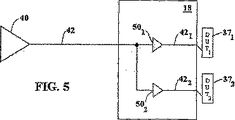
抵抗器減衰をもたらすことなく障害を分離するもう一つの方法は、チャネル分岐点それぞれとプローブとの間に分離バッファを含むことであるが、これについては図2に概略示され、かつ図5には一つのテストシステムについてさらに詳細に図示されている。図5において、テスタのドライバ40からの一つの伝送ラインチャネル42が、2つのIC371および372(それぞれ、テストを受ける装置“DUT”としてラベル付けされている)上のパッドに接触するための個別のプローブ421および422へチャネル信号を提供するために、プローブカード18における2つのバスライン501および502にファンアウトされる。もちろん、1つのチャネルは同様に複数のバスラインで、同じIC上の複数のパッドにファンアウトされることができる。
Another method of isolating faults without causing resistor attenuation is to include an isolation buffer between each channel branch and the probe, as schematically illustrated in FIG. 2 and in FIG. Is shown in more detail for one test system. In FIG. 5, one
分離バッファの一つの欠点は、すでに示されたように、分離バッファがテスタからウエハ上のDUTへのテスト信号の伝送に不確実な遅延をもたらすことである。遅延が不確実であるのは、バッファを通しての遅延は温度と給電電圧の変化と共に変化することがあり得るからである。テスタからウエハ上のDUTへの信号遅延は、ウエハのDUT上で一連のテストを行う間に変化し、不確実なテスト結果を生成することがあり得る。 One disadvantage of the isolation buffer is that, as already indicated, the isolation buffer introduces an uncertain delay in the transmission of test signals from the tester to the DUT on the wafer. The delay is uncertain because the delay through the buffer can change with changes in temperature and supply voltage. The signal delay from the tester to the DUT on the wafer may change during a series of tests on the wafer DUT, producing uncertain test results.
テストシステムで使用される分離バッファのもう一つの欠点は、テスタが、総括的にパラメトリックテストと称されることがあるDUT入力ピンオープン、ショートおよび漏れテストを行うことを、バッファが妨げることである。上に説明されたように、チャネルに導入されたバッファは、1つのライン上のショートあるいは開路の影響がもう一つのラインに影響を与えることを阻止するであろう。これは、分岐ラインを分離することの1つの利点を提供するけれども、故意にショートあるいは開路条件を使用してテストすることを妨げるであろう。同様に、1つのDUTからの漏れ電流は、バッファによって他のラインから阻止され、これはDUTからの漏れを測定することを妨げる条件となるであろう。
不等遅延をもたらすことなく、かつテスタがウエハのDUT上でパラメトリックテストを行うことを妨げることなく、信号を複数の伝送ラインに分配し、バッファを使用して障害からの分離を提供することが望ましい。 Distribute signals over multiple transmission lines and provide isolation from faults using buffers without introducing unequal delays and preventing the tester from performing parametric tests on the wafer DUT. desirable.
本発明により、テスタがウエハのDUT上で漏れおよびパラメトリックテストを行うことを妨げず、バッファを使用して障害を分離するために、回路構成が提供される。さらに、回路構成は複数の分離バッファを通しての遅延を一定に保つために提供される。 The present invention provides circuitry for isolating faults using a buffer without preventing the tester from performing leak and parametric tests on the wafer DUT. In addition, circuitry is provided to keep the delay through multiple isolation buffers constant.
本発明に従う構成要素を有するウエハテストシステムにおける分離バッファによって、プローブカードを、分岐して分離バッファを通るチャネルを有するプローブカードに単に変えることで、より効率的で費用効果の高いシステムが提供される。そのような分岐によって、プローバは、より多くのDUTをテストするために何度もウエハに接触するために位置を変えられる必要はない。しかし、テストカードに分岐を使用しなければ、この必要がある。単にプローブカードを分離バッファで置き換えるだけで、新しいテスタを購入するより別のもっと格段に安価な方法が提供されもする。 A separation buffer in a wafer test system having components according to the present invention provides a more efficient and cost effective system by simply changing the probe card into a probe card having a channel that branches off and passes through the separation buffer. . Such branching does not require the prober to be repositioned to contact the wafer over and over to test more DUTs. However, this is necessary unless branching is used in the test card. Simply replacing the probe card with a separation buffer also provides another much cheaper method than purchasing a new tester.
チャネルライン経路に含まれるバッファをパラメトリック、あるいは他の漏れテストに提供するために、漏れ電流が通過できるように、チャネルラインにおけるバッファの入力と出力との間に、バッファバイパス素子が提供される。漏れあるいはパラメトリックテスト測定の間、テストを受けつつあるラインにおけるバッファは不能とされることができ、唯一漏れ電流だけがバッファバイパス素子を通って測定されることができる。一つの実施形態においては、バッファバイパス素子は、バッファそれぞれの入力と出力との間に提供される既知値の抵抗器である。別の実施形態では伝送ゲートが、バッファそれぞれの入力と出力との間に提供される。電力およびアースをバッファから切り離すことに対する別の方法として、トライステートバッファが、漏れあるいはパラメトリックテストの間、バッファを不能とすることができるようにするために使用されることができる。 In order to provide a buffer included in the channel line path for parametric or other leakage tests, a buffer bypass element is provided between the input and output of the buffer in the channel line to allow leakage current to pass. During a leak or parametric test measurement, the buffer on the line under test can be disabled, and only the leakage current can be measured through the buffer bypass element. In one embodiment, the buffer bypass element is a known value resistor provided between the input and output of each buffer. In another embodiment, a transmission gate is provided between the input and output of each buffer. As an alternative to disconnecting power and ground from the buffer, a tri-state buffer can be used to allow the buffer to be disabled during a leak or parametric test.
さらに本発明によれば、テスト測定値から効果的にバッファ遅延を校正し出すために、リモートバッファを校正するための方法が提供される。第1校正方法は、有効バッファと共に、パラメトリックテストのためのテストモードと同様な漏れテストモードを使用し、さらに、時間領域反射率計(TDR)測定を使用する。バッファ遅延によってもたらされた中断は、漏れ電流のTDR測定において検知され、テスタがバッファ遅延を補正することを可能にする。第2の校正方法は、バッファ遅延のない個別のテスタチャネルを使用し、バッファ遅延を除去するためにバッファによる遅延チャネルと比較する。すべてのバッファが同じウエハ上にあるとすれば、第2の方法は、同じ測定されたバッファ遅延をすべてのバッファ付チャネルに適用することができる。第3の方法は、例えば、バッファ付きではないプローブカードを使用して測定された遅延など、既知の遅延を有するウエハあるいはDUTを使用する。次に、バッファ付プローブカードタイミングは、バッファ付プローブカードタイミングテスト結果が既知の装置の遅延を示すように調節されるであろう。 Further in accordance with the present invention, a method for calibrating a remote buffer is provided to effectively calibrate buffer delays from test measurements. The first calibration method uses a leak test mode similar to the test mode for parametric tests, along with a valid buffer, and further uses a time domain reflectometer (TDR) measurement. The interruption caused by the buffer delay is detected in the TDR measurement of the leakage current and allows the tester to correct the buffer delay. The second calibration method uses a separate tester channel with no buffer delay and compares it to a buffered delay channel to remove the buffer delay. Given that all buffers are on the same wafer, the second method can apply the same measured buffer delay to all buffered channels. The third method uses a wafer or DUT with a known delay, for example, a delay measured using a probe card that is not buffered. The buffered probe card timing will then be adjusted so that the buffered probe card timing test results indicate a known device delay.
分離バッファ遅延が均一であることを確かなものにするために、バッファ遅延は、給電電圧あるいは分離バッファそれぞれに提供された電流を制御する中央遅延制御回路によって制御される。遅延制御回路は基準遅延ラインおよび基準バッファの入力へ信号を提供する発振器を含む。基準遅延ラインおよび基準バッファは次に、位相比較器に入力を提供する。基準遅延ラインは、分離バッファの遅延を設定するために選択された長さを有する。位相比較器の出力は基準バッファおよび、分岐に提供された分離バッファを駆動するために、ループフィルタを通して提供される。構成されている通り、遅延制御回路は、システムにおける分離バッファそれぞれのように、基準バッファが基準遅延ラインに等しい遅延を提供するであろう遅延ロックループを実際上形成する。 In order to ensure that the isolation buffer delay is uniform, the buffer delay is controlled by a central delay control circuit that controls the supply voltage or current provided to each isolation buffer. The delay control circuit includes an oscillator that provides a signal to the input of the reference delay line and the reference buffer. The reference delay line and the reference buffer then provide an input to the phase comparator. The reference delay line has a length selected to set the delay of the isolation buffer. The output of the phase comparator is provided through a loop filter to drive a reference buffer and a separation buffer provided in the branch. As configured, the delay control circuit effectively forms a delay-locked loop where the reference buffer will provide a delay equal to the reference delay line, like each isolation buffer in the system.
分離バッファの遅延を変化させると、分離バッファそれぞれの出力電圧を変化させることにもなるので、さらなる実施形態においては、2つのバッファが、チャネル分岐点それぞれとプローブとの間で、順次使用される。第1バッファは可変遅延制御の適用を受ける一方、第2バッファは遅延制御を有さず、システムに、出力に変化のない電圧を供給することができる。 Since changing the delay of the isolation buffer also changes the output voltage of each isolation buffer, in a further embodiment, two buffers are used sequentially between each channel branch point and the probe. . While the first buffer is subject to variable delay control, the second buffer does not have delay control and can supply the system with a constant voltage at the output.
本発明のさらなる詳細が、添付された図面の助けで、以下説明される。 Further details of the invention are described below with the aid of the attached drawings.
図6は、バッファ50に供給されるバイアス電圧を変化させることのできる遅延制御を有する、分離バッファ50の実施形態である。図6において、バッファ50は、信号入力55および出力56を有するインバータ51を含む。システム給電電圧レール57および58は高圧V+および低圧V−を運ぶ。CMOS装置と共に、バイアスあるいは給電電圧は通常VddおよびVssと称される。通常、レール電圧V+およびV−はバッファに直接供給される。例えば、電圧V+は5ボルトであり得る一方、V−はアースあるいはゼロボルトであり得る。しかしながら、図6において、遅延制御回路は、給電電圧を変化させることによって遅延を制御するように設定され、電圧レールV+およびV−は、インバータ51へ高および低給電電圧として、それぞれの遅延制御回路60および61を通して提供される。図5および図6には、2つの分離遅延制御回路60および61として示されているけれども、単一合成回路が使用されることができる。さらに、2つの回路60および61は、V+およびV−電圧両方を変化させるように説明されているけれども、V+あるいはV−のうちいずれか1つが、望ましい遅延を達成するために、単独に変えられることができる。
FIG. 6 is an embodiment of an
バッファに供給される電圧を変化させることによってバッファ遅延を制御することが説明されたけれども、そのようにすることに付随する問題は、例えばインバータ51のようなバッファに供給される電圧の変化は、その出力56で供給される高および低電圧を変化させることである。本発明により、この問題は、図7に図解されているように、一対のインバータ(例えば、CMOSインバータ)として分離バッファそれぞれをインプリメントすることによって対処される。
Although it has been described that the buffer delay is controlled by changing the voltage supplied to the buffer, the problem with doing so is that the change in the voltage supplied to the buffer, eg, the
図7は、インバータ51と直列にインバータ52を加えるために図6を変更することによりバッファが構成される、そのようなインプリメンテーションを図解する。遅延は給電バイアス電圧を変化させることで制御され、第1インバータ51へ供給される電圧のみが、その遅延を制御するように変えられる。第2インバータ52への給電バイアス電圧はV+およびV−レールに固定されたままである。第2インバータ52の出力は、総合バッファ50の出力56であるので、総合バッファ50の高および低出力電圧はV+およびV−レールに固定されている。いくつかの場合においては、分離バッファ出力はV+およびV−レールに固定されたままでなくてはならないので、図7の回路は、固定給電電圧で第2インバータ52を使用する。
FIG. 7 illustrates such an implementation in which the buffer is constructed by modifying FIG. 6 to add inverter 52 in series with
異なった遅延制御回路が分離バッファそれぞれに提供され、温度および装置特性が分離バッファ間の遅延を変化させ得る。従って、分離バッファそれぞれによって提供される遅延を制御するために単一遅延制御回路が好ましい。複数の遅延制御回路に対比して、複数の分離バッファのための単一遅延制御回路の使用は、テストシステムに所望の総合回路構成を多大に減少させることもできる。 Different delay control circuits are provided for each isolation buffer, and temperature and device characteristics can vary the delay between isolation buffers. Therefore, a single delay control circuit is preferred to control the delay provided by each isolation buffer. In contrast to multiple delay control circuits, the use of a single delay control circuit for multiple isolation buffers can also greatly reduce the overall circuit configuration desired for the test system.
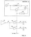
複数のバッファの遅延を制御するための単一遅延制御回路の詳細は図8に示されている。遅延回路70は、図5同様、ウエハテスタ構成の2つの分離バッファ501、および502に接続されて示されている。しかしながら、遅延制御回路70は同様に、3つ以上の分離バッファへ提供されることができ、あるいは、例えばクロックツリーのようなウエハテスタ以外の他のタイプの回路の分岐において提供されることができる。さらに、当業者に理解されるであろうように、図示されている遅延制御回路70は、図5および図6に示される遅延制御回路60および61の組み合わせ、あるいは遅延制御回路60および61の個別のものとして機能するように構成されることができる。
Details of a single delay control circuit for controlling the delay of multiple buffers are shown in FIG. The delay circuit 70 is shown connected to two
遅延制御回路70は、基準遅延ライン74および基準バッファ76両方の入力へ提供される周期信号を生成するために発振器か、あるいはクロック生成器72を含む。発振器は直列接続のインバータあるいは、例えば抵抗器などのような遅延素子と直列のインバータから構成されることができる。発振器信号周波数およびデューティサイクルは重大ではない、というのは、誤差信号は、同時に基準遅延ライン74および基準バッファ76へ入力される発振器の、同じ周期あるいはサイクルの立上がりおよび立下りエッジから来るのみであるからである。
The delay control circuit 70 includes an oscillator or
基準遅延ライン74は、分離バッファ501および502を通る望ましい遅延に等しい遅延を有するように構成される。基準遅延ライン74の次元は、当業者によって理解されるであろうように、遅延ライン74を通る遅延を制御するように設定されることができる。基準遅延ライン74は、分離バッファ501および502、基準バッファ76、位相比較器78その他を含む集積回路上に構成されることができるか、あるいはそのような集積回路の外部に提供されることができる。集積回路上の構成要素の物理的次元は、リソグラフィーで制御されることができるので、部分ごとの差異は最小限にされることができる。絶対あるいは相対遅延のさらに正確な制御が所望される、要求の厳しいアプリケーションにおいては、レーザトリミングが遅延ライン74を同調するために適用されることができる。レーザトリミングなしでは、伝送ライン遅延における若干の差異は、伝送ラインを構成するために使用された材料あるいは物質のTceのためにもたらされ得る。このような場合、伝送ラインの比較的小さな遅延差異は遅延ロックループを同調することにより安定化されることができる。
位相比較器78は、基準遅延ライン74および基準バッファ76からの出力の位相における相違を測定する。位相比較器78の出力は低域フィルタすなわち、ループフィルタ回路80を駆動する。フィルタ80は、位相誤差に比例する制御電圧を生成するために位相比較器信号をフィルタリングする。この位相誤差制御電圧は次に、基準バッファ76の遅延を調節するために使用される。電圧制御基準バッファ76、位相比較器78および低域フィルタ80の組み合わせは普通、「遅延ロックループ」と称される。このように、遅延制御回路70は、基準バッファ76に、タイムプロセスおよび温度から独立した基準を提供し、さらに、制御電圧を、例えば501および502などのような複数の分離バッファに印加する。
図8の遅延制御回路70は、基準バッファ76を通る遅延を強制して基準遅延ライン74を通る遅延に合わせる。基準遅延ライン74を通る遅延は通常は、周囲の条件(例えば、温度あるいは給電の電圧)によって変化しないので、遅延制御回路70は、周囲の温度あるいは、その給電の電圧における変化にもかかわらず、基準バッファ76を通る遅延を一定に保つ。
The delay control circuit 70 of FIG. 8 forces the delay through the reference buffer 76 to match the delay through the
図8の遅延制御回路70はさらに、単一チャネル42とDUT371および372の間の分岐421および422において提供される分離バッファ501および502のバイアス電圧を制御する。このようにして、遅延制御回路70は、基準バッファ76および分離バッファ501および502を通る遅延を一定に保つ傾向がある。2つの分離バッファ501および502が図示されているけれども、図解されているように、他の分岐に提供されたさらなるバッファは回路70によって遅延を制御され得る。
The delay control circuit 70 of FIG. 8 further controls the bias voltage of the isolation buffers 50 1 and 50 2 provided in the
遅延制御回路70は、バッファ遅延を設定するために、基準バッファ76および分離バッファ501および502に供給されている電圧V+およびV−のいずれか、あるいは両方ともを制御するために接続されることができる。このようにして、ループフィルタ80からの接続は、V−あるいはV+のうちの1つからの変化した電圧を提供するための単一ラインかあるいは、V+およびV−それぞれからの変化した電圧を提供するための2つのラインを有するバスか、いずれかであることができる。
The delay control circuit 70 is connected to control either or both of the voltages V + and V− supplied to the reference buffer 76 and the isolation buffers 50 1 and 50 2 to set the buffer delay. be able to. In this way, the connection from the
バッファ間の遅延が実質的に同じになることを確かなものにするために、基準バッファ76および分離バッファ501、502その他はできるだけ同様であるべきであり、あるいは少なくとも分離バッファ501および502を通る遅延を受容できる相違以内に保つために必要なくらい同様であるべきである。基準バッファ76および分離バッファ501および502は同じウエハで製造され、かつ同様な装置および温度特性を確かなものにするために、できるなら同じICチップ上に提供されることができることが好ましい。 To ensure that the delay between the buffers is substantially the same, the reference buffer 76 and the isolation buffers 50 1 , 50 2, etc. should be as similar as possible, or at least the isolation buffers 50 1 and 50. Should be as similar as necessary to keep the delay through 2 within acceptable differences. Reference buffer 76 and isolation buffers 50 1 and 50 2 are preferably manufactured on the same wafer and can be provided on the same IC chip if possible to ensure similar device and temperature characteristics.
基準バッファ76および、分離バッファ501および502は図6に示される単一インバータ構成かあるいは、図7に示される直列インバータであるか、いずれかであることができる。図6の単一インバータ構成であれば、遅延制御回路70は、バッファインバータのすべてに供給される給電電圧のいずれか、あるいは両方ともを制御する。図7の直列インバータ構成であれば、遅延回路70は、直列の第1インバータの給電バイアス電圧を制御する一方、給電電圧は第2直列インバータのため、V+およびV−に固定されたままとなる。図7の分離バッファ構成であれば、基準バッファ76および分離バッファ501および502の両方ともが、遅延がバッファそれぞれにおいて実質的に同じ値に正確に制御されるように、基準および分離バッファの間の類似性を最大限にするために直列インバータを含むほうが好ましい。 Reference buffer 76 and isolation buffers 50 1 and 50 2 can be either a single inverter configuration as shown in FIG. 6 or a series inverter as shown in FIG. With the single inverter configuration of FIG. 6, the delay control circuit 70 controls either or both of the supply voltages supplied to all of the buffer inverters. With the series inverter configuration of FIG. 7, delay circuit 70 controls the feed bias voltage of the first inverter in series, while the feed voltage remains fixed at V + and V− because of the second series inverter. . With the isolation buffer configuration of FIG. 7, both the reference buffer 76 and the isolation buffers 50 1 and 50 2 have the reference and isolation buffer's so that the delay is precisely controlled to substantially the same value in each of the buffers. In order to maximize the similarity between them, it is preferable to include a series inverter.
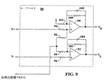
図9は低域フィルタすなわち、ループフィルタ80のための1つの実施形態の詳細を示す。図8に示されるように、ループフィルタ80は、位相比較器78の出力を統合し、かつV+およびV−システム電圧レール間に集中した基準バッファ76および分離バッファ501および502に2つの集中遅延制御電圧VHおよびVLを提供するように機能する。図9に示される回路は、ループフィルタ80のための1つの実施形態を提供するが、フィルタデザインは重大ではなく、当業者に理解されるであろうように、別の低域フィルタ回路構成によって取って代わられることができる。例えば、コンデンサおよび抵抗器を使用する受動低域フィルタは、能動素子増幅器90および92を含む図9に示されるループ回路80に取って代わることができよう。
FIG. 9 shows details of one embodiment for the low pass filter, ie,
図9のループフィルタ回路80は入力として、給電レール電圧V+およびV−および位相比較器78の出力を受信する。これらの入力から、図9の回路は制御電圧VHおよびVLを生成する。電圧VHは高給電入力(すなわち、CMOSインバータのためのVdd入力)として、基準バッファ76および分離バッファに提供される一方、VLは低給電入力(すなわち、CMOSインバータのためのVss入力)として、基準バッファ76および分離バッファに提供される。
The
ループフィルタ80は2つの差動増幅器90および92を含む。増幅器90の出力は制御電圧VHを提供する一方、増幅器92の出力は制御電圧VLを提供する。抵抗器94はレール電圧V+を増幅器90の非反転(+)入力に接続する一方、抵抗器96はレール電圧V−を増幅器92の非反転(+)入力に接続する。位相比較器78からの出力は抵抗器98を通して増幅器90の非反転(+)入力へ、かつ抵抗器99を通して増幅器92の反転(−)入力へ接続される。フィードバックが、反転入力をアースに接続する抵抗器101と共に、抵抗器100およびその出力をその反転(−)入力に接続するコンデンサ103によって増幅器90において提供される。フィードバックが抵抗器102および、その出力をその反転(−)入力に接続するコンデンサ104によって増幅器92において提供される。フィードバックコンデンサ103および104は、増幅器90および92が、ノイズを減じるための積算器として機能することを可能にする。抵抗器94、96、98および99は、電圧VHおよびVLがV+およびV−の間に集中することを確かなものにするために機能する。
多数のバッファを駆動するために、電力増幅器がVHおよびVL出力を増幅するために加えられ得る。また、コンデンサはVHおよびVL出力と分離バッファのそれぞれの入力との間に置くことが望ましい。そのようなコンデンサは給電からの高周波ノイズをフィルタリングする。 In order to drive multiple buffers, power amplifiers can be added to amplify the V H and V L outputs. Also, the capacitors are preferably placed between the VH and VL outputs and the respective inputs of the isolation buffer. Such a capacitor filters high frequency noise from the power supply.
図9の回路は、分離バッファの出力でのデジタル信号がその給電入力を変化させることがないように、かつV+およびV−との間の給電レベルに集中されるようにデザインされている。そうすることによって、次の回路の遷移は、V+およびV−レベルが変化を受けないままであるときのように、信号の立上がりあるいは立下りエッジにおいて、およそ等しい時間に起きるであろう。分離バッファの出力をV+およびV−の間に集中させないことによって、1つのエッジは次の回路遷移を通常よりも早く誘発し、誤ったテスト結果が生じる原因となるであろう。 The circuit of FIG. 9 is designed so that the digital signal at the output of the isolation buffer does not change its power supply input and is concentrated on the power supply level between V + and V−. By doing so, the next circuit transition will occur at approximately equal times on the rising or falling edge of the signal, as when the V + and V- levels remain unchanged. By not concentrating the output of the isolation buffer between V + and V-, one edge will trigger the next circuit transition earlier than usual, causing false test results.
図9に示される回路構成では、位相比較器78からの位相差信号出力が大きければ大きいほど、VHおよびVLとの間の相違も大きい。分離バッファに適用された場合、バッファ遅延制御回路70からのVHおよびVLとの間の相違が大きければ大きいほど、分離バッファによって提供される遅延は小さい。
In the circuit configuration shown in FIG. 9, the larger the phase difference signal output from the
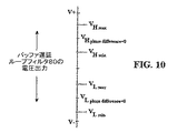
図10は、図9の回路からのVHおよびVL信号出力に対する作動範囲を図解する図表を示す。VHおよびVLの範囲は抵抗器94、96、98および99に対して選ばれた値に依存する。VHおよびVLとの間のセンタライン電圧が同じにとどまることを確かなものにするために、位相差の変化と共に、等しい差異がVHおよびVLにおいて起きるように抵抗器94、96、98および99は選ばれる方が好ましい。位相比較器78からの位相差出力信号がゼロのときは、VHはその範囲全体の中央にあり、かつVLはその範囲全体の中央にあるように、抵抗器の値はさらに選ばれる。VHおよびVLに対する特定の範囲は、インプリメントされる特別な回路の要求次第で変化するであろう。
FIG. 10 shows a diagram illustrating the operating range for the V H and V L signal outputs from the circuit of FIG. The range of V H and V L depends on the values chosen for
図11は所望の回路構成を全体的に減らすために構成された、図8の分離バッファおよび遅延制御回路に対する別法を示す。図11において、単一可変遅延分離バッファ110が、分岐点の前のチャネル、あるいは伝送ライン42に置かれる。インバータとして示されている分離バッファ110は、その遅延を設定するために遅延制御回路70から可変給電バイアス信号VLおよびVHを受け取る。固定遅延バッファ1121および1122は、そのとき、ファンアウト点の後で分岐421および422に含まれている。バッファ1121および1122はまたインバータとしても図示されているが、システム給電レールから固定給電入力V+およびV−を受け取る。2つのバッファ1121および1122が示されているが、ファンアウトは3つ以上へなされることができよう。
FIG. 11 illustrates an alternative to the isolation buffer and delay control circuit of FIG. 8 configured to reduce the overall desired circuit configuration. In FIG. 11, a single variable
図11の直列インバータ114および116は図8の基準バッファ76の代わりを務める。インバータ114は、ループフィルタ80から可変給電バイアス信号VLおよびVHを受け取る。インバータ116は固定給電レールV+およびV−を受け取る。インバータはすべて、同様な装置および温度差異特性を生成するために、同じ半導体ウエハ上で製造されることを含んで、できるだけ同様に製造されることが好ましい。かくて、図11の回路は、分離バッファに1つの共通チャネルからのファンアウトを提供し、均一な遅延を生成する。図11の回路は、図7に示されるようにバッファを使用する図8の回路に勝る利点を提供する、というのは分岐点それぞれにおいて、ただ1つのバッファが必要とされているからである。
The series inverters 114 and 116 in FIG. 11 take the place of the reference buffer 76 in FIG.
図12は、直列CMOSインバータによって形成された図7の分離バッファのための実施形態を図解するが、インバータ51は単一遅延制御回路160によって遅延が制御される一方、インバータ52は固定遅延を有する。遅延制御回路160は、図11の遅延制御回路70同様、図7の回路60および61の機能を組み合わせる。CMOSインバータ51は、図11の回路70同様、遅延制御回路160から生成された遅延制御電圧VHおよびVLを受け取るPMOSトランジスタ121およびNMOSトランジスタ120を含む。CMOSインバータ52は同様にPMOSおよびNMOSトランジスタを含み、これらトランジスタは固定V−およびV+電圧レールによって駆動される。
FIG. 12 illustrates an embodiment for the isolation buffer of FIG. 7 formed by a series CMOS inverter, where
図13は、図12の回路において変化する電圧に対比して、遅延が電流を変化させることによって制御される分離バッファ構成を図解する。図13はさらに、バッファは、CMOSインバータと対比して、例えば二極接合トランジスタ(BJT)を使用して作成された差動増幅器など、他の構成をとることができることを図解する。図示されているように、図13のバッファ51は、電流が遅延制御回路161によって制御される電流シンク130を有する差動増幅器である。1つの実施形態においては、遅延制御回路161は図8の回路70として構成されることができる。遅延制御回路161のそのような構成においては、図8のループフィルタ80の出力は、差動増幅器および差動増幅器バッファ51として構成された基準バッファ76の電流入力を供給するであろう。図13のバッファ51は、+および−差動増幅器入力を形成するバス、電流シンク130へ接続された共通エミッタおよび抵抗器136および138を通してV+給電レールに提供されたコレクタを有するBJTトランジスタ132および134を含む。
FIG. 13 illustrates an isolation buffer configuration in which the delay is controlled by changing the current as opposed to the voltage changing in the circuit of FIG. FIG. 13 further illustrates that the buffer can take other configurations, for example, a differential amplifier made using a bipolar junction transistor (BJT), as opposed to a CMOS inverter. As shown, the
差動増幅器51は単独で使用されることができるか、あるいは、もしレールからレールへの単一出力が望まれるならば、第2の増幅器52を通して出力56へ接続されることができる。差動増幅器51はレールからレールへのV+およびV−電圧を分配しないであろう、というのは、抵抗器136および138ならびに電流シンク130は出力スイングを制限するからである。レールからレールへの出力が望まれるならば、図13に示されるように、V+およびV−レールへ接続された制御電圧VOHおよびVOLで比較器として構成された増幅器52が所望のレールからレールへのスイングを提供するであろう。
図14は、パラメトリックテストのための漏れ電流測定を可能にするために、分離バッファ501−3の入力と出力との間の抵抗器1401−3によって提供されたバッファバイパス素子がチャネル42の分岐において提供された分離バッファ501−3を示す。抵抗器1401−3を使用して提供されたバイパス素子はきわめて低い電流漏れ測定を可能にする。低い漏れ測定に便宜を図るために、既知値の抵抗器1401−3はバッファ501−3それぞれの入力および出力との間に接続される。図15は、図11の配置同様、複数のバッファ110および1121−3を横断する抵抗器1401−3を使用してバッファバイパス素子を提供するための、図14の回路構成に対する変型例を図解する。
FIG. 14 shows that the buffer bypass element provided by the
図14および図15の構成で漏れ電流を測定するために、漏れ測定の間、バッファすべておよび測定されている途中ではないDUTへの電力およびアースは、給電とバッファとの間および給電とDUTとの間に提供された高インピーダンス抵抗スイッチあるいはリレー(図示されず)を使用して切断される。次に、電圧が抵抗器1401−3全部にわたって強制され、その結果生じる電流が、給電に接続されたままであったDUTすべてに対して測定される。バッファおよび使用されていないDUTは同様に、パラメトリックテストのためには動作不能となっている。
To measure leakage current in the configurations of FIGS. 14 and 15, during the leakage measurement, the power and ground to all buffers and the DUT not being measured are between the power supply and the buffer and between the power supply and the DUT. Is disconnected using a high impedance resistance switch or relay (not shown) provided between the two. The voltage is then forced across
図16は、チャネルにおいて提供されているバッファ1501−2に対しての漏れおよびパラメトリックテストを可能にするために、伝送ゲート1451−2を使用してバッファバイパス素子を提供するためのもう1つの実施形態を示す。伝送ゲート1451−2がバッファ1501−2それぞれの入力および出力の間に提供される。伝送ゲート1451−2が、並列に接続されたソースドレイン経路および制御入力を提供するために、インバータを通して共に接続されたゲートを有するPMOSおよびNMOSトランジスタで、標準的なCMOS装置として形成されることができる。伝送ゲート1451−2は同様に、バッファおよび制御を提供するゲートを横断して接続されたソースドレイン経路を有する単一PMOSあるいはNMOSトランジスタから形成されることができる。伝送ゲートは同様に、異なるトランジスタのタイプを使用して、例えばBJTトランジスタなどを使用することによって、形成されることができる。図16は、もし望まれるならば、伝送ゲート1451−2を使用して、複数のバッファ110および1121−2を横断してバッファバイパス素子を提供するための、図17の回路構成に対する変型例を図解する。
FIG. 16 illustrates another one for providing a buffer bypass element using
パラメトリックテストに伝送ゲート1451−2を提供するために、1つの実施形態において、バッファ1501−2あるいは1121−2は、テストを受けるDUTへ接続された伝送ゲートが動作可能にされている間、トライステートモードに置かれる。このことを図解するために、出力イネーブル信号OEは、図16−17において、異なる時間に、トライステートバッファおよび伝送ゲートを動作可能にするために逆極性が提供されて示されている。この実施形態は、より大きな漏れ値を測定するために適切であり、かつバッファ装置の電力とアースの切断は必要ではないであろう。同様に、電力は、テストを受けている途中にないDUTへ接続されたままであることができよう。図17の構成で、バッファ110はトライステートバッファではない、というのは、その信号経路はバッファ1121−2によって阻止されているからである。しかしながら、バッファ110からの漏れがテスト測定に影響を与えるならば、トライステート装置としてバッファ110を有することが望ましい。図17の構成はさらに、図11について説明されたように、遅延制御回路からのより少ない数のラインを使用する。
In order to provide
本発明はさらに、本発明により説明されたように、バッファバイパス素子を有するバッファでシステムを校正するための方法を提供する。校正は、バッファ遅延が、バッファを含むチャネルラインを使用して出されたテスト結果から校正されることができるように、バッファを通る遅延の指示を提供する。校正手順は、図14−17において示されている回路構成のうち、いずれを使用しても実施されることができる。 The present invention further provides a method for calibrating a system with a buffer having a buffer bypass element, as described by the present invention. The calibration provides an indication of the delay through the buffer so that the buffer delay can be calibrated from the test results issued using the channel line that contains the buffer. The calibration procedure can be implemented using any of the circuit configurations shown in FIGS. 14-17.
第1構成方法は、バッファあるいは能動であるバッファと共なる、かつさらに従来の時間領域反射率(TDR)測定と共なるバッファバイパス素子(漏れテストモードで動作可能にされている)を通して提供された漏れ電流のテストを使用する。バッファ遅延によってもたらされた不連続は、TDR比較器を使用して検知され、かつ測定され、このようにして、テストシステムのテスタがバッファ遅延を差し引くことによって計算し、テストシステムにおけるバッファのために補償することを可能にする。TDR測定において、テストパルスが提供され、かつ反射パルスはバッファ入力および出力から測定される。バッファの入力および出力からの反射の受け取りの間での時間差は、バッファを通る遅延の決定のために使用される。同様な計算は、複数のバッファがチャネルにおいて直列で提供されていれば、他のバッファに対しても使用される。 The first configuration method was provided through a buffer bypass element (enabled in leak test mode) with a buffer or active buffer and also with a conventional time domain reflectivity (TDR) measurement. Use a leakage current test. The discontinuity caused by the buffer delay is detected and measured using a TDR comparator, and thus calculated by the test system tester by subtracting the buffer delay and for the buffer in the test system. Makes it possible to compensate. In TDR measurement, a test pulse is provided and the reflected pulse is measured from the buffer input and output. The time difference between receiving the reflection from the buffer input and output is used to determine the delay through the buffer. Similar calculations are used for other buffers if multiple buffers are provided in series in the channel.
図18−19は異なる長さの遅延を提供するバッファでTDR測定を使用しての、バッファ遅延の決定を図解するタイミング図である。図18は、TDR測定装置から提供されたパルス160、およびパルスがバッファ遅延とおよそ同じバッファの入力と出力からの、結果として生じたリターン反射162および164を示す。図18に示されているように、バッファ遅延は、バッファの入力と出力からの反射162および164の立上がりエッジ間の時間差を測定することによって決定される。図19は、TDR装置から提供されたパルス170およびパルスがバッファ遅延よりも小さい、結果として生じるリターン反射172および174を示す。バッファの入力および出力からの反射パルス172および174は分離されているけれども、2つの反射パルス172および174の立上がりエッジの間の同様な測定はバッファ遅延を決定する。
18-19 are timing diagrams illustrating the determination of buffer delay using TDR measurements with buffers providing different lengths of delay. FIG. 18 shows the
バッファ遅延を決定し除去するための第2校正方法においては、個別の比較テストチャネルが、バッファを含むチャネルから使用される。測定が、チャネルに接続された共通の装置の遅延を決定するためになされ、かつ結果の比較がなされ、その相違がバッファ遅延を示す。テストシステムにおけるバッファすべてが同じダイ上にあれば、あるいは同じ温度で同じウエハからであれば、この方法は、1つのバッファに対するバッファ遅延決定が、バッファ付チャネルすべてのためのバッファ遅延として使用されることを可能にする。 In a second calibration method for determining and removing buffer delay, a separate comparison test channel is used from the channel containing the buffer. A measurement is made to determine the delay of a common device connected to the channel and a comparison of the results is made, the difference indicating the buffer delay. If all the buffers in the test system are on the same die or from the same wafer at the same temperature, this method uses the buffer delay determination for one buffer as the buffer delay for all buffered channels. Make it possible.
バッファ遅延を決定し除去するための第3校正方法においては、既知のあるいは校正された遅延を有するウエハあるいは他のDUTが使用される。テスト装置の遅延が、バッファ付ではないチャネルを使って決定されることができる。次に、測定がバッファ付チャネルに対してなされ、バッファ付チャネルの測定値は、既知の装置の校正された遅延以外の遅延を差し引くことによって、バッファから生じるいかなる遅延も実際的に校正するために調整される。 In a third calibration method for determining and removing buffer delays, a wafer or other DUT with a known or calibrated delay is used. The delay of the test equipment can be determined using a non-buffered channel. Next, a measurement is made on the buffered channel, and the buffered channel measurement is used to practically calibrate any delay resulting from the buffer by subtracting a delay other than the calibrated delay of the known device. Adjusted.
本発明は以上、細目にわたって説明されたけれども、これは単に当業者に本発明の作成および使用方法を教示するためであった。多くのさらなる変型例が本発明の範囲内に入るし、その範囲は次の特許請求の範囲によって規定されている通りである。 Although the present invention has been described in detail above, this was merely to teach one of ordinary skill in the art how to make and use the invention. Many further variations fall within the scope of the invention, which is as defined by the following claims.
Claims (19)
該テストチャネルにおいて、該分離バッファの信号入力と出力との間に提供されたバッファバイパス素子と、
該電子デバイスに接触するように構成されたテストプローブと
を含み、
該テストチャネルは、該電子デバイスのテストを制御するためにテスタの1つの端部において電気的に接続しており、該テストプローブの別の端部において終端するように構成され、
前記バッファバイパス素子が伝送ゲートを含み、
信号が、トライステートバッファが動作可能にされるときには前記伝送ゲートを動作不能にするために、該トライステートバッファが動作不能にされるときには該伝送ゲートを動作可能にするために提供される、装置。An isolation buffer provided in a test channel of a test system for testing an electronic device;
A buffer bypass element provided between the signal input and output of the isolation buffer in the test channel;
A test probe configured to contact the electronic device; and
The test channel is configured to electrically connect at one end of a tester to control testing of the electronic device and to terminate at another end of the test probe ;
The buffer bypass element includes a transmission gate;
An apparatus is provided for disabling the transmission gate when the tri-state buffer is enabled and for enabling the transmission gate when the tri-state buffer is disabled. .
該分離バッファと並列に提供されたバッファバイパス素子と、
該電子デバイスのテストを制御するために該テストチャネルをテスタに電気的に接続するように構成された電気的インターフェースと、
該電子デバイスに接触するように構成されたテストプローブと
を含み、
該電気的インターフェースは、該テストプローブに電気的に接続され、
前記バッファバイパス素子が伝送ゲートを含み、
信号が、トライステートバッファが動作可能にされるときには前記伝送ゲートを動作不能にするために、該トライステートバッファが動作不能にされるときには該伝送ゲートを動作可能にするために提供される、装置。An isolation buffer provided in a test channel for testing electronic devices;
A buffer bypass element provided in parallel with the isolation buffer;
An electrical interface configured to electrically connect the test channel to a tester to control testing of the electronic device;
A test probe configured to contact the electronic device; and
The electrical interface is electrically connected to the test probe ;
The buffer bypass element includes a transmission gate;
An apparatus is provided for disabling the transmission gate when the tri-state buffer is enabled and for enabling the transmission gate when the tri-state buffer is disabled. .
該電子デバイスのうちの1つに接触するように構成された、該信号ラインから複数のテストプローブまでの複数の分岐と、
分離バッファであって、該分離バッファのそれぞれは該分岐のうちの一つにおいて提供される、分離バッファと、
バッファバイパス素子であって、該バッファバイパス素子それぞれは該分離バッファのうちの1つと電気的に並列に接続されている、バッファバイパス素子と
を含み、
前記バッファバイパス素子は伝送ゲートを含み、
前記信号ラインにおいて提供されるさらなるバッファであって、前記分離バッファの入力に接続される出力を有するさらなるバッファをさらに含み、前記バッファバイパス素子は該さらなるバッファの入力と該分離バッファのうちの1つの出力とに電気的に接続され、
前記さらなるバッファはトライステートバッファを含み、
信号が、前記トライステートバッファが動作可能にされるときには前記伝送ゲートを動作不能にするため、該トライステートバッファが動作不能とされるときには該伝送ゲートを動作可能とするために提供される、装置。A signal line configured to electrically connect to a tester for testing the electronic device;
A plurality of branches from the signal line to a plurality of test probes configured to contact one of the electronic devices;
A separation buffer, each of the separation buffers being provided in one of the branches;
A buffer bypass element, respectively the buffer bypass elements are connected to one electrical parallel of the separation buffer, viewed contains a buffer bypass element,
The buffer bypass element includes a transmission gate;
A further buffer provided in the signal line, further comprising a buffer having an output connected to an input of the isolation buffer, wherein the buffer bypass element is one of the input of the additional buffer and one of the isolation buffers Electrically connected to the output,
The further buffer comprises a tri-state buffer;
An apparatus is provided for disabling the transmission gate when the tri-state buffer is enabled, and for enabling the transmission gate when the tri-state buffer is disabled. .
前記さらなる分離バッファの出力は、前記分離バッファの入力に接続されており、
それぞれのバイパス素子は、該さらなる分離バッファの入力と該分離バッファのうちの1つの出力とに接続されている、請求項15に記載の装置。In the at least one of the test channels,
The output of the further separation buffer is connected to the input of the separation buffer;
16. The apparatus of claim 15 , wherein each bypass element is connected to an input of the further isolation buffer and an output of one of the isolation buffers.
テストされるべき複数の電子デバイスに接触するように構成された複数のテストプローブであって、それぞれの分岐は、該複数のテストプローブのうちの1つにおいて終端している、複数のテストプローブと、
該分岐のうちのそれぞれの分岐において提供されている複数の分離バッファと、
複数のバッファバイパス素子であって、それぞれのバッファバイパス素子は、該分離バッファのうちの1つと電気的に並列に接続されている、バッファバイパス素子と
をさらに含んでいる、請求項1に記載の装置。The test channel includes a common signal line electrically connected to a plurality of branch signal lines, and the apparatus includes:
A plurality of test probes configured to contact a plurality of electronic devices to be tested, each branch terminating in one of the plurality of test probes; ,
A plurality of isolation buffers provided in each of the branches;
The buffer bypass element according to claim 1, further comprising: a plurality of buffer bypass elements, each buffer bypass element being electrically connected in parallel with one of the isolation buffers. apparatus.
Applications Claiming Priority (3)
| Application Number | Priority Date | Filing Date | Title |
|---|---|---|---|
| US10/937,470 | 2004-09-09 | ||
| US10/937,470 US7453258B2 (en) | 2004-09-09 | 2004-09-09 | Method and apparatus for remotely buffering test channels |
| PCT/US2005/032202 WO2006029340A2 (en) | 2004-09-09 | 2005-09-08 | Method and apparatus for remotely buffering test channels |
Publications (3)
| Publication Number | Publication Date |
|---|---|
| JP2008512682A JP2008512682A (en) | 2008-04-24 |
| JP2008512682A5 JP2008512682A5 (en) | 2008-10-23 |
| JP4950051B2 true JP4950051B2 (en) | 2012-06-13 |
Family
ID=35995565
Family Applications (1)
| Application Number | Title | Priority Date | Filing Date |
|---|---|---|---|
| JP2007531379A Expired - Fee Related JP4950051B2 (en) | 2004-09-09 | 2005-09-08 | Device for buffering test channels remotely |
Country Status (7)
| Country | Link |
|---|---|
| US (2) | US7453258B2 (en) |
| EP (1) | EP1794607A2 (en) |
| JP (1) | JP4950051B2 (en) |
| KR (1) | KR101207090B1 (en) |
| CN (2) | CN101115998B (en) |
| TW (1) | TWI401447B (en) |
| WO (1) | WO2006029340A2 (en) |
Families Citing this family (25)
| Publication number | Priority date | Publication date | Assignee | Title |
|---|---|---|---|---|
| US7262611B2 (en) * | 2000-03-17 | 2007-08-28 | Formfactor, Inc. | Apparatuses and methods for planarizing a semiconductor contactor |
| US7365556B2 (en) * | 2004-09-02 | 2008-04-29 | Texas Instruments Incorporated | Semiconductor device testing |
| US7453258B2 (en) | 2004-09-09 | 2008-11-18 | Formfactor, Inc. | Method and apparatus for remotely buffering test channels |
| US7262624B2 (en) * | 2004-12-21 | 2007-08-28 | Formfactor, Inc. | Bi-directional buffer for interfacing test system channel |
| US7653356B2 (en) * | 2005-09-15 | 2010-01-26 | Silicon Laboratories Inc. | System and method for reducing spurious emissions in a wireless communication device including a testing apparatus |
| US7890822B2 (en) * | 2006-09-29 | 2011-02-15 | Teradyne, Inc. | Tester input/output sharing |
| US7852094B2 (en) * | 2006-12-06 | 2010-12-14 | Formfactor, Inc. | Sharing resources in a system for testing semiconductor devices |
| JP2009071533A (en) * | 2007-09-12 | 2009-04-02 | Advantest Corp | Differential signal transmitter and test device |
| US20090085598A1 (en) * | 2007-09-28 | 2009-04-02 | Qimonda Ag | Integrated circuit test system and method with test driver sharing |
| JP2011226854A (en) * | 2010-04-16 | 2011-11-10 | Advantest Corp | Voltage supply apparatus |
| KR101133030B1 (en) * | 2010-12-08 | 2012-04-04 | 인텔릭스(주) | System of built in self test for discrete |
| US9399324B2 (en) | 2011-06-29 | 2016-07-26 | Dow Global Technologies Llc | Flame resistant composition, fiber reinforced polyurethane based composite comprising the flame resistant composition and the use thereof |
| US8680888B2 (en) * | 2011-12-15 | 2014-03-25 | Micron Technologies, Inc. | Methods and systems for routing in a state machine |
| US8928383B2 (en) * | 2013-03-15 | 2015-01-06 | Analog Devices, Inc. | Integrated delayed clock for high speed isolated SPI communication |
| TWI467195B (en) * | 2013-06-17 | 2015-01-01 | Ardentek Corp | Testing method for contact interfaces of test system |
| CN104931759B (en) * | 2014-03-21 | 2018-07-06 | 中芯国际集成电路制造(上海)有限公司 | A kind of test circuit and test method of standard block leakage current |
| US9696376B2 (en) * | 2015-03-12 | 2017-07-04 | Globalfoundries Inc. | Leakage testing of integrated circuits using a logarithmic transducer and a voltmeter |
| US10302677B2 (en) * | 2015-04-29 | 2019-05-28 | Kla-Tencor Corporation | Multiple pin probes with support for performing parallel measurements |
| KR102576210B1 (en) | 2016-07-05 | 2023-09-08 | 삼성전자주식회사 | Semiconductor device |
| JP6782134B2 (en) * | 2016-09-26 | 2020-11-11 | ラピスセミコンダクタ株式会社 | Scan circuits, collective scan circuits, semiconductor devices, and semiconductor device inspection methods |
| KR102336181B1 (en) | 2017-06-07 | 2021-12-07 | 삼성전자주식회사 | Leakage current measurement circuit, integrated circuit and system including same |
| US20190250208A1 (en) * | 2018-02-09 | 2019-08-15 | Qualcomm Incorporated | Apparatus and method for detecting damage to an integrated circuit |
| KR102549004B1 (en) * | 2018-06-22 | 2023-06-29 | 삼성디스플레이 주식회사 | Lighting test device, lighting test method and lighting test system |
| US11313903B2 (en) * | 2020-09-30 | 2022-04-26 | Analog Devices, Inc. | Pin driver and test equipment calibration |
| CN113866589A (en) * | 2021-09-03 | 2021-12-31 | 长江存储科技有限责任公司 | Chip testing device and chip testing method |
Family Cites Families (27)
| Publication number | Priority date | Publication date | Assignee | Title |
|---|---|---|---|---|
| JPH0812529B2 (en) * | 1989-06-07 | 1996-02-07 | キヤノン株式会社 | Fixing device |
| JP3005250B2 (en) * | 1989-06-30 | 2000-01-31 | テキサス インスツルメンツ インコーポレイテツド | Bus monitor integrated circuit |
| JPH05172900A (en) * | 1991-12-20 | 1993-07-13 | Yokogawa Electric Corp | Pulse transmission line |
| JPH0720206A (en) * | 1993-06-23 | 1995-01-24 | Kawasaki Steel Corp | Output circuit for oscillation circuit |
| JP3080847B2 (en) * | 1994-10-05 | 2000-08-28 | 日本電気株式会社 | Semiconductor storage device |
| US5594694A (en) | 1995-07-28 | 1997-01-14 | Micron Quantum Devices, Inc. | Memory circuit with switch for selectively connecting an input/output pad directly to a nonvolatile memory cell |
| US5790459A (en) | 1995-08-04 | 1998-08-04 | Micron Quantum Devices, Inc. | Memory circuit for performing threshold voltage tests on cells of a memory array |
| KR19980702516A (en) * | 1995-12-28 | 1998-07-15 | 오오우라 히로시 | Semiconductor integrated circuit device having delay error correction circuit |
| US6239604B1 (en) * | 1996-10-04 | 2001-05-29 | U.S. Philips Corporation | Method for inspecting an integrated circuit by measuring a voltage drop in a supply line of sub-circuit thereof |
| US5966318A (en) * | 1996-12-17 | 1999-10-12 | Raytheon Company | Nondestructive readout memory utilizing ferroelectric capacitors isolated from bitlines by buffer amplifiers |
| JPH11231022A (en) * | 1998-02-13 | 1999-08-27 | Matsushita Electric Ind Co Ltd | Inspection method of semiconductor device and device thereof |
| JPH11326441A (en) * | 1998-05-20 | 1999-11-26 | Advantest Corp | Semiconductor testing device |
| US6055287A (en) * | 1998-05-26 | 2000-04-25 | Mcewan; Thomas E. | Phase-comparator-less delay locked loop |
| US6442674B1 (en) * | 1998-12-30 | 2002-08-27 | Intel Corporation | Method and system for bypassing a fill buffer located along a first instruction path |
| US6157231A (en) * | 1999-03-19 | 2000-12-05 | Credence System Corporation | Delay stabilization system for an integrated circuit |
| EP1049167A3 (en) * | 1999-04-30 | 2007-10-24 | Sel Semiconductor Energy Laboratory Co., Ltd. | Semiconductor device and manufacturing method thereof |
| US6377067B1 (en) * | 2000-02-01 | 2002-04-23 | Winbond Electronics Corporation | Testing method for buried strap and deep trench leakage current |
| US6603323B1 (en) * | 2000-07-10 | 2003-08-05 | Formfactor, Inc. | Closed-grid bus architecture for wafer interconnect structure |
| JP4717295B2 (en) * | 2000-10-04 | 2011-07-06 | 株式会社半導体エネルギー研究所 | Dry etching apparatus and etching method |
| US6445228B1 (en) * | 2001-08-28 | 2002-09-03 | Xilinx, Inc. | Programmable even-number clock divider circuit with duty cycle correction and optional phase shift |
| JP2003279625A (en) * | 2002-03-27 | 2003-10-02 | Toshiba Microelectronics Corp | Semiconductor integrated circuit |
| JP3703794B2 (en) * | 2002-11-05 | 2005-10-05 | 日本電子材料株式会社 | Probes and probe cards |
| JP2004170079A (en) * | 2002-11-15 | 2004-06-17 | Hitachi Electronics Eng Co Ltd | Testing waveform supply method, semiconductor testing method, driver, and semiconductor testing apparatust |
| US7250772B2 (en) * | 2002-11-19 | 2007-07-31 | University Of Utah Research Foundation | Method and apparatus for characterizing a signal path carrying an operational signal |
| JP2004198269A (en) * | 2002-12-19 | 2004-07-15 | Hitachi Ltd | Semiconductor integrated circuit device |
| US7154259B2 (en) | 2003-10-23 | 2006-12-26 | Formfactor, Inc. | Isolation buffers with controlled equal time delays |
| US7453258B2 (en) | 2004-09-09 | 2008-11-18 | Formfactor, Inc. | Method and apparatus for remotely buffering test channels |
-
2004
- 2004-09-09 US US10/937,470 patent/US7453258B2/en not_active Expired - Fee Related
-
2005
- 2005-09-08 JP JP2007531379A patent/JP4950051B2/en not_active Expired - Fee Related
- 2005-09-08 CN CN2005800297017A patent/CN101115998B/en not_active Expired - Fee Related
- 2005-09-08 KR KR1020077008051A patent/KR101207090B1/en not_active IP Right Cessation
- 2005-09-08 CN CN201010536273XA patent/CN102053221A/en active Pending
- 2005-09-08 WO PCT/US2005/032202 patent/WO2006029340A2/en active Application Filing
- 2005-09-08 EP EP05795133A patent/EP1794607A2/en not_active Withdrawn
- 2005-09-09 TW TW094131190A patent/TWI401447B/en not_active IP Right Cessation
-
2008
- 2008-11-18 US US12/273,408 patent/US7825652B2/en not_active Expired - Fee Related
Also Published As
| Publication number | Publication date |
|---|---|
| CN101115998B (en) | 2011-01-05 |
| WO2006029340A2 (en) | 2006-03-16 |
| CN101115998A (en) | 2008-01-30 |
| US7825652B2 (en) | 2010-11-02 |
| US20090132190A1 (en) | 2009-05-21 |
| US7453258B2 (en) | 2008-11-18 |
| TW200624841A (en) | 2006-07-16 |
| US20060049820A1 (en) | 2006-03-09 |
| KR20070100695A (en) | 2007-10-11 |
| EP1794607A2 (en) | 2007-06-13 |
| CN102053221A (en) | 2011-05-11 |
| TWI401447B (en) | 2013-07-11 |
| JP2008512682A (en) | 2008-04-24 |
| KR101207090B1 (en) | 2012-11-30 |
| WO2006029340A3 (en) | 2007-07-26 |
Similar Documents
| Publication | Publication Date | Title |
|---|---|---|
| JP4950051B2 (en) | Device for buffering test channels remotely | |
| US7362092B2 (en) | Isolation buffers with controlled equal time delays | |
| US6586921B1 (en) | Method and circuit for testing DC parameters of circuit input and output nodes | |
| US5617035A (en) | Method for testing integrated devices | |
| US7109736B2 (en) | System for measuring signal path resistance for an integrated circuit tester interconnect structure | |
| JP4255284B2 (en) | Single-ended channel calibration for differential operation | |
| KR100731344B1 (en) | Circuit and method for improved test and calibration in automated test equipment | |
| US9551741B2 (en) | Current tests for I/O interface connectors | |
| US10481204B2 (en) | Methods and systems to measure a signal on an integrated circuit die | |
| US7200170B1 (en) | High speed I-O loopback testing with low speed DC test capability | |
| US6262585B1 (en) | Apparatus for I/O leakage self-test in an integrated circuit | |
| US20210302493A1 (en) | Integrated circuit with embedded testing circuitry | |
| WO2008056206A1 (en) | Method for testing noise immunity of an integrated circuit and a device having noise immunity testing capabilities | |
| JP3558425B2 (en) | Signal switching device and switch circuit | |
| Muhtaroglu et al. | I/O self-leakage test | |
| Lanzoni et al. | An experimental study of testing techniques for bridging faults in CMOS ICs | |
| Rajinita et al. | Improving testability and fault analysis in low level design |
Legal Events
| Date | Code | Title | Description |
|---|---|---|---|
| A521 | Written amendment |
Free format text: JAPANESE INTERMEDIATE CODE: A523 Effective date: 20080903 |
|
| A621 | Written request for application examination |
Free format text: JAPANESE INTERMEDIATE CODE: A621 Effective date: 20080903 |
|
| RD02 | Notification of acceptance of power of attorney |
Free format text: JAPANESE INTERMEDIATE CODE: A7422 Effective date: 20100527 |
|
| RD04 | Notification of resignation of power of attorney |
Free format text: JAPANESE INTERMEDIATE CODE: A7424 Effective date: 20110204 |
|
| A977 | Report on retrieval |
Free format text: JAPANESE INTERMEDIATE CODE: A971007 Effective date: 20110914 |
|
| A131 | Notification of reasons for refusal |
Free format text: JAPANESE INTERMEDIATE CODE: A131 Effective date: 20110920 |
|
| A601 | Written request for extension of time |
Free format text: JAPANESE INTERMEDIATE CODE: A601 Effective date: 20111220 |
|
| A602 | Written permission of extension of time |
Free format text: JAPANESE INTERMEDIATE CODE: A602 Effective date: 20111228 |
|
| A521 | Written amendment |
Free format text: JAPANESE INTERMEDIATE CODE: A523 Effective date: 20120119 |
|
| TRDD | Decision of grant or rejection written | ||
| A01 | Written decision to grant a patent or to grant a registration (utility model) |
Free format text: JAPANESE INTERMEDIATE CODE: A01 Effective date: 20120209 |
|
| A01 | Written decision to grant a patent or to grant a registration (utility model) |
Free format text: JAPANESE INTERMEDIATE CODE: A01 |
|
| A61 | First payment of annual fees (during grant procedure) |
Free format text: JAPANESE INTERMEDIATE CODE: A61 Effective date: 20120308 |
|
| FPAY | Renewal fee payment (event date is renewal date of database) |
Free format text: PAYMENT UNTIL: 20150316 Year of fee payment: 3 |
|
| R150 | Certificate of patent or registration of utility model |
Free format text: JAPANESE INTERMEDIATE CODE: R150 |
|
| LAPS | Cancellation because of no payment of annual fees |