JP4946366B2 - Multilayer capacitor - Google Patents
Multilayer capacitor Download PDFInfo
- Publication number
- JP4946366B2 JP4946366B2 JP2006302929A JP2006302929A JP4946366B2 JP 4946366 B2 JP4946366 B2 JP 4946366B2 JP 2006302929 A JP2006302929 A JP 2006302929A JP 2006302929 A JP2006302929 A JP 2006302929A JP 4946366 B2 JP4946366 B2 JP 4946366B2
- Authority
- JP
- Japan
- Prior art keywords
- electrode
- internal electrode
- multilayer capacitor
- dielectric layer
- insulated
- Prior art date
- Legal status (The legal status is an assumption and is not a legal conclusion. Google has not performed a legal analysis and makes no representation as to the accuracy of the status listed.)
- Active
Links
Images


Landscapes
- Ceramic Capacitors (AREA)
- Fixed Capacitors And Capacitor Manufacturing Machines (AREA)
Description
この発明は、積層コンデンサに関し、特に、電子基板用の部品としての積層コンデンサに関する。 The present invention relates to a multilayer capacitor, and more particularly to a multilayer capacitor as a component for an electronic substrate.
従来、電子基板用の部品として広く用いられている積層セラミックコンデンサが知られている。この積層セラミックコンデンサは、高Q化、即ち大容量化と低抵抗化や、製造歩留まりや製品寿命の向上が図られている。
例えば、従来の「積層コンデンサ」(特許文献1参照)では、低抵抗化のために内部電極を広くすると所定のコンデンサ容量とならず、電極を厚くすると誘電体内の応力が高くなって割れ等が発生することが説明されている。そして、対応策として、内部電極を厚くするのではなく、同電位の薄い電極を複数枚用いて構成することにより、コンデンサ容量を変えずに内部発生応力を低減することが開示されている。
Conventionally, a multilayer ceramic capacitor widely used as a component for an electronic substrate is known. In this multilayer ceramic capacitor, high Q, that is, large capacity and low resistance, and improvement in manufacturing yield and product life are achieved.
For example, in the conventional “multilayer capacitor” (see Patent Document 1), if the internal electrode is widened to reduce the resistance, the predetermined capacitor capacity is not obtained, and if the electrode is thickened, the stress in the dielectric increases and cracks occur. It is explained that it occurs. As a countermeasure, it is disclosed that the internal stress is reduced without changing the capacitor capacity by using a plurality of thin electrodes having the same potential instead of increasing the thickness of the internal electrode.
また、従来の「積層セラミック電子部品」(特許文献2参照)では、外部電極への接続幅を小さくすることで誘電体同士の密着度を向上させると共に、内部電極の角部積層方向に一致しないようにして内部応力を低減し、製造歩留まりや製品寿命を向上させている。
しかしながら、近年の大容量インバータへの積層コンデンサの適用に際しては、コンデンサ容量の増大と大電流化が要求されていることから、同電位の薄い電極を複数枚用いて構成した積層セラミックコンデンサを適用させようとした場合、同電位電極で挟まれた誘電体部分が無駄となり容量低下の原因となってしまう。また、外部電極への接続幅を小さくした部分での電流集中による内部抵抗発熱が顕著となり、導体断面積が小さくなったこととも相俟って、高抵抗化してしまうことが避けられない。 However, in the application of multilayer capacitors to large-capacity inverters in recent years, it is required to increase the capacitor capacity and increase the current. Therefore, multilayer ceramic capacitors composed of multiple thin electrodes with the same potential are applied. In such a case, the dielectric portion sandwiched between the same potential electrodes is wasted and causes a reduction in capacity. Further, internal resistance heat generation due to current concentration becomes remarkable at the portion where the connection width to the external electrode is reduced, and it is inevitable that the resistance is increased in combination with the reduction of the conductor cross-sectional area.
更に、現在の積層セラミックコンデンサの形状では、両端の外部電極がハンダ付けされており、そのハンダを介して冷却されているため、冷却を強化することができなかった。加えて、コンデンサ形状である長方体の6面にそれぞれ電極が形成され、特に、6面中4面には両電極が形成されているため、絶縁部材を介するしか導電性ヒートシンク等へ伝熱することができず、効果的な冷却を外部から行うことは困難であった。
この発明の目的は、大容量化及び大電流化が可能な上に外部からの強制冷却も可能になる積層コンデンサを提供することである。
Furthermore, in the present multilayer ceramic capacitor shape, the external electrodes at both ends are soldered and cooled via the solder, so that the cooling cannot be enhanced. In addition, electrodes are formed on each of the six faces of the capacitor-shaped rectangular parallelepiped, and in particular, since both electrodes are formed on four of the six faces, heat is transferred to the conductive heat sink or the like only via an insulating member. It was not possible to perform effective cooling from the outside.
An object of the present invention is to provide a multilayer capacitor that can increase the capacity and current and can be forcedly cooled from the outside.
上記目的を達成するため、この発明に係る積層コンデンサは、複数の誘電体層と複数の内部電極層を交互に積み重ねた積層コンデンサにおいて、前記各内部電極層を交互に並列接続する一対の電極接続部を設け、前記一対の電極接続部の少なくとも一方が、積層方向の一方端側と絶縁されており、前記一方端側に誘電体層を介して導電性の冷却器が接触していることを特徴としている。また、複数の誘電体層と複数の内部電極層を交互に積み重ねた積層コンデンサにおいて、前記各内部電極層を交互に並列接続する一対の電極接続部を設け、前記一対の電極接続部の少なくとも一方が、積層方向の一方端側と絶縁されており、前記一方端側に、絶縁されている側の電極接続部と外部電極との接触部を設け、積層方向の他方端側に、絶縁されていない側の電極接続部が外部電極に接続されると共に、該外部電極を介して導電性の冷却器が接触していることを特徴としている。 To achieve the above object, a multilayer capacitor according to the present invention is a multilayer capacitor in which a plurality of dielectric layers and a plurality of internal electrode layers are alternately stacked, and a pair of electrode connections that alternately connect the internal electrode layers in parallel. And at least one of the pair of electrode connection portions is insulated from one end side in the stacking direction , and a conductive cooler is in contact with the one end side through a dielectric layer. It is a feature. Further, in the multilayer capacitor in which a plurality of dielectric layers and a plurality of internal electrode layers are alternately stacked, a pair of electrode connection portions for alternately connecting the internal electrode layers in parallel is provided, and at least one of the pair of electrode connection portions Is insulated from one end side in the laminating direction, provided with a contact portion between the insulated electrode connecting portion and the external electrode on the one end side, and insulated from the other end side in the laminating direction. The non-side electrode connecting portion is connected to the external electrode, and a conductive cooler is in contact with the external electrode via the external electrode.
この発明によれば、複数の誘電体層と複数の内部電極層を交互に積み重ねた積層コンデンサは、各内部電極層を交互に並列接続して設けられた一対の電極接続部の少なくとも一方が、積層方向の一方端側と絶縁されており、前記一方端側に誘電体層を介して導電性の冷却器が接触していることから、絶縁されている面を、導電性の冷却手段により直接冷却することができ、また、各内部電極層を交互に並列接続する一対の電極接続部を設け、一対の電極接続部の少なくとも一方が、積層方向の一方端側と絶縁されており、一方端側に、絶縁されている側の電極接続部と外部電極との接触部を設け、積層方向の他方端側に、絶縁されていない側の電極接続部が外部電極に接続されると共に、外部電極を介して導電性の冷却器が接触していることから、広い面積で外部電極と電気接続していると共に、最下部誘電体層と冷却手段との間にあって、伝熱冷却の助けとなっている。このため、積層コンデンサの電流耐量を増加させることができ、大容量化及び大電流化が可能な上に外部からの強制冷却も可能になる。 According to the present invention, in the multilayer capacitor in which the plurality of dielectric layers and the plurality of internal electrode layers are alternately stacked, at least one of the pair of electrode connection portions provided by alternately connecting the internal electrode layers in parallel is: Since it is insulated from one end side in the stacking direction , and a conductive cooler is in contact with the one end side through a dielectric layer , the insulated surface is directly connected by a conductive cooling means. A pair of electrode connection portions that alternately connect the internal electrode layers in parallel, and at least one of the pair of electrode connection portions is insulated from one end side in the stacking direction; A contact portion between the insulated electrode connecting portion and the external electrode is provided on the side, and the non-insulated electrode connecting portion is connected to the external electrode on the other end side in the stacking direction. The conductive cooler is in contact via Et al., With are external electrodes electrically connected in a wide area, there between the cooling means and the bottom dielectric layer, which is conducive to heat transfer cooling. For this reason, the withstand current of the multilayer capacitor can be increased, the capacity and current can be increased, and forced cooling from the outside is also possible.
以下、この発明を実施するための最良の形態について図面を参照して説明する。
(第1実施の形態)
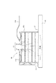
図1は、この発明の第1実施の形態に係る積層コンデンサの断面図である。図1に示すように、積層コンデンサである積層セラミックコンデンサ10は、誘電体を矩形薄板状に形成した誘電体層11と内部電極を矩形薄板状に形成した内部電極層12を、それぞれ複数個交互に積み重ねて形成した、例えば、直方体形状の素体13を有している。この積層セラミックコンデンサ10は、素体13の上端面で一対の外部電極14a,14bに接続されていると共に、冷却器15に載置されている。
The best mode for carrying out the present invention will be described below with reference to the drawings.
(First embodiment)
FIG. 1 is a cross-sectional view of the multilayer capacitor in accordance with the first embodiment of the present invention. As shown in FIG. 1, a multilayer ceramic capacitor 10 which is a multilayer capacitor includes a plurality of
この素体13の積層方向に交差する両側端面には、内部電極層12が積層順に交互に並列に接続されている一対のペースト電極(電極接続部)16a,16bが設けられている。各ペースト電極16a,16bは、素体13の側端面から素体13の積層方向上端に位置する上端面に延びる側面視L字形状(図1参照)を有しており、導電性ペーストを塗布した後焼成して形成されている。つまり、端部L字ペースト電極焼成タイプ(片面よせ)である。
A pair of paste electrodes (electrode connecting portions) 16a and 16b, in which the
各ペースト電極16a,16bは、素体13の両側端面側の下端が、素体13の下端面から離間する長さに形成されており、素体13の下端面との間に、間隙a或いはレジスト17を設けている。ペースト電極16aの下端は間隙aにより、ペースト電極16bの下端はレジスト17により、それぞれ冷却器15と接触することなく絶縁された状態にある。また、各ペースト電極16a,16bの上端は、素体13の上端面、即ち、誘電体層11の上面を覆うと共に、互いに上端面の略中央で接触することなく隙間を有して配置されている。そして、ペースト電極16aには外部電極14aが、ペースト電極16bには外部電極14bが、それぞれが接続されている。
Each
このように、冷却器15に載置された積層セラミックコンデンサ10は、誘電体層11が冷却器15に接触した状態で、両外部電極14a,14bのそれぞれが接続された、一対のペースト電極16a,16bの少なくとも一方が、素体13の積層方向両端側、即ち、上下端面の何れか一方と絶縁されており、絶縁されているペースト電極は、上下端面の絶縁されていない端面まで延長されている。なお、図1においては、両ペースト電極16a,16bが、素体13の下端面と絶縁されると共に上端面まで延長された状態を例示しており、素体13の上面で外部電極14a,14bを介して電気接続されている。
As described above, the multilayer ceramic capacitor 10 placed on the
即ち、内部電極同士を並列接続する導電性ペーストを最下部誘電体層に塗らないことで、下面(下端面)に接している冷却部との絶縁が保たれている。絶縁を保持するために、最下部誘電体層に絶縁被膜を塗布しても良い。また、導電性ペーストを上面(上端面)まで塗ることにより、上面での外部電極との接続を容易にしている。
従って、積層セラミックコンデンサ10は、冷却器15に接触する誘電体層11を介して冷却することができ、内部電極層12が素体13の外表面に露出していることから、電気接続がし易い。
(第2実施の形態)
That is, the conductive paste that connects the internal electrodes in parallel is not applied to the lowermost dielectric layer, so that the insulation from the cooling part in contact with the lower surface (lower end surface) is maintained. In order to maintain insulation, an insulating film may be applied to the lowermost dielectric layer. Further, the conductive paste is applied to the upper surface (upper end surface), thereby facilitating connection with the external electrode on the upper surface.
Therefore, the multilayer ceramic capacitor 10 can be cooled via the
(Second Embodiment)
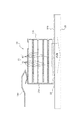
図2は、この発明の第2実施の形態に係る積層コンデンサの断面図である。図2に示すように、積層セラミックコンデンサ20は、ペースト電極16a,16bに代えて、素体13の各側端面から上下各端面に延びる側面視L字形状(図2参照)のペースト電極21a,21bを有している。
つまり、ペースト電極21aは、素体13の一方の側端面全域とこの側端面に続く上端面に、ペースト電極21bは、素体13の他方の側端面全域とこの側端面に続く下端面に、それぞれ配置されており、素体13の上端面で外部電極14aに、下端面で外部電極14bに、それぞれ接続されている。その他の構成及び作用は積層セラミックコンデンサ10(図1参照)と同様である。
FIG. 2 is a cross-sectional view of the multilayer capacitor in accordance with the second embodiment of the present invention. As shown in FIG. 2, the multilayer
That is, the
両ペースト電極21a,21bは、素体13の上端面及び下端面で互いに接触することなく隙間を有して配置されており、導電性ペーストを側端面と上端面或いは下端面にL字型に塗布(0.5工程増加)した後焼成して形成する、端部L字ペースト電極焼成タイプである。また、外部電極14bに接続されているペースト電極21aの下端部は、冷却器15の間にレジスト22を介在させている。
なお、図中、ペースト電極21aは下端面に、ペースト電極21bは上端面に、それぞれ延び出た状態に示されているが、これは、塗布時に形成されるものであって無視できるものである。
Both the
In the drawing, the
このように、積層セラミックコンデンサ20は、通常の積層セラミックコンデンサ構造を有しているが、外部電極接続用のペースト電極21a,21bを、素体13の側端面と上端面或いは下端面にかかるL字型に配置している。即ち、一方の側端面のペースト電極21bが下面に回り込み、広い面積で外部電極と電気接続していると共に、最下部誘電体層と冷却器15との間にあって、伝熱冷却の助けとなっている。加えて、電気接続がし易い。
As described above, the multilayer
図3は、図2の積層コンデンサの他の例を示す断面図である。図3に示すように、積層セラミックコンデンサ25は、ペースト電極21a,21bを、素体13の両側端面全域に配置するのではなく、ペースト電極21aは下端部を素体13の底面から離間して、ペースト電極21bは上端部を素体13の上面から離間して、それぞれ配置されている。その他の構造及び作用は、積層セラミックコンデンサ20と同様である。
つまり、積層セラミックコンデンサ25は、素体13の側面の一部と上端面或いは下端面にかかるL字型に、導電性ペーストを塗布した後焼成して形成した端部L字ペースト電極焼成タイプ(但し、端部部分塗り)の、外部電極接続用のペースト電極21a,21bを配置している。
(第3実施の形態)
FIG. 3 is a cross-sectional view showing another example of the multilayer capacitor of FIG. As shown in FIG. 3, in the multilayer
That is, the multilayer
(Third embodiment)
図4は、この発明の第3実施の形態に係る積層コンデンサの断面図である。図4に示すように、積層セラミックコンデンサ30は、素体13の最下層の誘電体層、即ち、冷却器15に接触する誘電体層が、積層方向長さである厚さを薄くして形成されている。その他の構成及び作用は積層セラミックコンデンサ10(図1参照)と同様である。
また、この積層セラミックコンデンサ30の最上層の誘電体層の厚さは、最下層の誘電体層の薄さに対応して厚く形成し、合計の厚さを同一にしている。これにより、素体13の外径寸法を、最下層の誘電体層を薄くしない場合と変わらなくすることができる。
FIG. 4 is a cross-sectional view of the multilayer capacitor in accordance with the third embodiment of the present invention. As shown in FIG. 4, the multilayer
The thickness of the uppermost dielectric layer of the multilayer
このように、最下層の誘電体層11の厚さはコンデンサ容量と無関係であることから、誘電体層11の厚みを薄くすることで冷却熱抵抗を低下させ、冷却能力を向上させることができる。また、外径寸法が変わらないので、従来のデバイスと同様に実装することができる。
(第4実施の形態)
As described above, since the thickness of the
(Fourth embodiment)
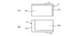
図5は、この発明の第4実施の形態に係る積層コンデンサの第1電極パターンを示し、(a)は陽極側内部電極の平面図、(b)は陰極側内部電極の平面図である。図6は、この発明の第4実施の形態に係る積層コンデンサの第2電極パターンを示し、(a)は陽極側内部電極の平面図、(b)は陰極側内部電極の平面図である。図7は、この発明の第4実施の形態に係る積層コンデンサの第3電極パターンを示し、(a)は陽極側内部電極の平面図、(b)は陰極側内部電極の平面図である。 FIG. 5 shows the first electrode pattern of the multilayer capacitor in accordance with the fourth embodiment of the present invention, wherein (a) is a plan view of the anode side internal electrode, and (b) is a plan view of the cathode side internal electrode. 6A and 6B show a second electrode pattern of the multilayer capacitor in accordance with the fourth embodiment of the present invention. FIG. 6A is a plan view of the anode side internal electrode, and FIG. 6B is a plan view of the cathode side internal electrode. 7A and 7B show a third electrode pattern of the multilayer capacitor in accordance with the fourth embodiment of the present invention. FIG. 7A is a plan view of the anode side internal electrode, and FIG. 7B is a plan view of the cathode side internal electrode.
図5から図7に示す、積層セラミックコンデンサの外部電極接続用ペースト電極のパターン例は、これまでは主に二面に形成していたペースト電極の面数を、熱引きを良くするために増やしたものである。長方形板体状に形成された内部電極層12の陽極側(陽極側内部電極)と陰極側(陰極側内部電極)の組み合わせによる、例えば、第1電極パターンから第3電極パターンの3パターンを説明する。
The pattern examples of the paste electrodes for connecting the external electrodes of the multilayer ceramic capacitor shown in FIGS. 5 to 7 increase the number of paste electrodes formed so far mainly on two surfaces to improve heat dissipation. It is a thing. Explain, for example, three patterns from the first electrode pattern to the third electrode pattern by combining the anode side (anode side internal electrode) and cathode side (cathode side internal electrode) of the
図5に示すように、第1電極パターンは、陽極側内部電極35aを、誘電体層11の一方の短辺11a及び両長辺11c,11dの3辺側に、誘電体層11が露出して陽極側内部電極35aが形成されないコ字状縁部を有するように、形成する((a)参照)。陰極側内部電極36aを、誘電体層11の他方の短辺11b側に、誘電体層11が露出して陰極側内部電極36aが形成されないI字状縁部を有するように、形成する((b)参照)。
As shown in FIG. 5, in the first electrode pattern, the anode-side
つまり、一方のペースト電極に接続された陰極側内部電極36aを、4側端面の1面である誘電体層11の他方の短辺11b側に、他方のペースト電極に接続された陽極側内部電極35aを、4側端面の残りの3面である、誘電体層11の一方の短辺11a及び両長辺11c,11dの3辺側に露出させている。
この電極パターンの場合、ペースト電極の塗りが、左浅く1回、右深く1回でできる。
That is, the cathode side
In the case of this electrode pattern, the paste electrode can be applied once shallowly on the left and once deeply on the right.
図6に示すように、第2電極パターンは、陽極側内部電極35bを、誘電体層11の一方の短辺11a側に、誘電体層11が露出して陽極側内部電極35bが形成されないI字状縁部を有するように、形成する((a)参照)。陰極側内部電極36aを、誘電体層11の他方の短辺11b側に、誘電体層11が露出して陰極側内部電極36aが形成されないI字状縁部を有するように、形成する((b)参照)。この電極パターンの場合、ペースト電極の塗りを簡略化しつつ、容量を最大にすることができる。
As shown in FIG. 6, in the second electrode pattern, the anode-side
図7に示すように、第3電極パターンは、陽極側内部電極35cを、誘電体層11の一方の短辺11a及び一方の長辺11cの2辺側に、誘電体層11が露出して陽極側内部電極35cが形成されないL字状縁部を有するように、形成する((a)参照)。陰極側内部電極36bを、誘電体層11の他方の短辺11b及び他方の長辺11dの2辺側に、誘電体層11が露出して陰極側内部電極36bが形成されないL字状縁部を有するように、形成する((b)参照)。
As shown in FIG. 7, the third electrode pattern is such that the anode-side
つまり、一方のペースト電極に接続された陽極側内部電極35cを、4側端面の2面に、他方のペースト電極に接続された陰極側内部電極36bを、4側端面の残りの2面に露出させている。
この電極パターンの場合、ペースト電極の塗り工程は複雑になるが、両電極共に均等に抜熱することができるので、焼成工程時やデバイスとしての使用時に割れることがない。
That is, the anode-side
In the case of this electrode pattern, the paste electrode coating process is complicated, but since both electrodes can be uniformly removed, they are not cracked during the firing process or when used as a device.
上述した、第1から第3の電極パターンに示すように、内部電極の形状を工夫したことで、ペースト電極による並列接続面積を広くなって抵抗が小さくなり、素子特性が改善すると共に冷却能力の改善にも寄与する。
図8は、図5の第1パターンによる素体形成の説明図である。図8に示すように、上面に陽極側内部電極35aを形成した誘電体層11と、上面に陰極側内部電極36aを形成した誘電体層11とを、交互に積み重ねて、誘電体層11を挟んで陽極側内部電極35aと陰極側内部電極36aが交互に積層された積層体を形成する。
As shown in the first to third electrode patterns described above, by devising the shape of the internal electrode, the parallel connection area by the paste electrode is increased, the resistance is reduced, the device characteristics are improved, and the cooling capacity is improved. Contributes to improvement.
FIG. 8 is an explanatory diagram of element formation by the first pattern of FIG. As shown in FIG. 8, the
この積層体に、誘電体層11の一方の短辺11a側から浅く、他方の短辺11b側から深く、それぞれ1回ずつペースト電極を塗布し、一方の短辺11a側と、他方の短辺11b及び一方の短辺11aに接触しない両長辺11c,11dの3辺側に、ペースト電極塗布面37を形成する。ペースト電極塗布面37を形成した後、焼成して、積層体の側面に陽極側内部電極35a及び陰極側内部電極36aに接続するペースト電極を形成する。
図9は、図6の第2パターンによる素体形成の説明図である。図9に示すように、上面に陽極側内部電極35bを形成した誘電体層11と、上面に陰極側内部電極36aを形成した誘電体層11とを、交互に積み重ねて、誘電体層11を挟んで陽極側内部電極35bと陰極側内部電極36aが交互に積層された積層体を形成する。
A paste electrode is applied to the multilayer body once each from the
FIG. 9 is an explanatory diagram of element formation by the second pattern of FIG. As shown in FIG. 9, the
この積層体に、誘電体層11の一方の短辺11a側と他方の短辺11b側から、それぞれペースト電極を塗布し、一方の短辺11a側と他方の短辺11b側に、ペースト電極塗布面37を形成する。ペースト電極塗布面37を形成した後、焼成して、積層体の側面に陽極側内部電極35a及び陰極側内部電極36aに接続するペースト電極を形成する。
図10は、図7の第3パターンによる素体形成の説明図である。図10に示すように、上面に陽極側内部電極35cを形成した誘電体層11と、上面に陰極側内部電極36bを形成した誘電体層11とを、交互に積み重ねて、誘電体層11を挟んで陽極側内部電極35cと陰極側内部電極36bが交互に積層された積層体を形成する。
A paste electrode is applied to the laminated body from one
FIG. 10 is an explanatory diagram of element formation by the third pattern of FIG. As shown in FIG. 10, the
この積層体に、誘電体層11の一方の短辺11a側と他方の短辺11b側から、それぞれペースト電極を塗布し、一方の短辺11aと一方の長辺11c、及び他方の短辺11bと他方の長辺11dが、それぞれに接触しないように、一方の短辺11a側に連続する他方の長辺11d側、及び他方の短辺11側に連続する一方の長辺11c側に、ペースト電極塗布面37を形成する。ペースト電極塗布面37を形成した後、焼成して、積層体の側面に陽極側内部電極35a及び陰極側内部電極36aに接続するペースト電極を形成する。
(第5実施の形態)
Paste electrodes are applied to the laminate from one
(Fifth embodiment)
図11は、この発明の第5実施の形態に係る積層コンデンサの内部電極を示し、(a)は内部電極否形成部を有する場合の平面図、(b)は切欠部を有する場合の平面図である。図11に示すように、誘電体層11の上面に形成する内部電極(陽極内部電極や陰極内部電極)40の角部や辺部に、誘電体層11の上面が露出する、例えば円形状の内部電極否形成部41を設ける((a)参照)。つまり、誘電体層11の上面に、内部電極40を形成しない部分を設ける。これにより、積み重ねられた上下の誘電体層11の密着性が向上し、重ね合わせ・焼成工程で層間の剥がれ、即ち、内部電極の剥がれを防止することができる。
11A and 11B show internal electrodes of a multilayer capacitor in accordance with a fifth embodiment of the present invention. FIG. 11A is a plan view in the case of having an internal electrode non-forming portion, and FIG. 11B is a plan view in the case of having a notch portion. It is. As shown in FIG. 11, the upper surface of the
また、誘電体層11の上面に形成する内部電極(陽極内部電極や陰極内部電極)40の角部を、尖端が形成されないように、丸く切り欠いた切欠部42((b)参照)。これにより、電流や応力が集中しないようにすることができる。
(第6実施の形態)
図12は、この発明の第6実施の形態に係る積層コンデンサの層構造説明図である。図12に示すように、積層セラミックコンデンサの素体45は、誘電体層11の上面に形成する陽極側内部電極46a及び陰極側内部電極46bの少なくとも一方を、積層方向長さを長く、即ち、厚く形成する。
Further, a corner portion of an internal electrode (anode internal electrode or cathode internal electrode) 40 formed on the upper surface of the
(Sixth embodiment)
FIG. 12 is an explanatory diagram of the layer structure of the multilayer capacitor in accordance with the sixth embodiment of the present invention. As shown in FIG. 12, the
つまり、例えば、上面に、厚い陽極側内部電極46aを形成した誘電体層11と、上面に、薄い陰極側内部電極46bを形成した誘電体層11とを、交互に積み重ねて、誘電体層11を挟んで陽極側内部電極46aと陰極側内部電極46bが交互に積層された積層体を形成する。
このように、電極形成部材の厚塗り或いは重ね塗り等により内部電極を厚肉に形成したことにより、伝熱性の高い内部金属電極の厚さを増加させて側方への熱伝達性を良くし、内部電極における水平方向熱引き性を改善することができる。
なお、陽極側内部電極46a及び陰極側内部電極46bの両方ではなく、一方のみ厚くした場合、陽極側内部電極46a及び陰極側内部電極46bの両方を厚くする場合に比べて、工程の増加分が半分になる。
That is, for example, the
In this way, by forming the internal electrode thickly by thick coating or overcoating of the electrode forming member, the thickness of the internal metal electrode having high heat conductivity is increased and the heat transfer to the side is improved. In addition, it is possible to improve the heat dissipation property in the horizontal direction in the internal electrode.
It should be noted that when only one of the anode side
上述したように、この発明に係る積層コンデンサは、複数の誘電体層と複数の内部電極層を交互に積み重ねた積層コンデンサにおいて、前記各内部電極層を交互に並列接続する一対の電極接続部を設け、前記一対の電極接続部の少なくとも一方が、積層方向の一方端側と絶縁されており、前記一方端側に誘電体層を介して導電性の冷却器が接触している。また、前記誘電体層と前記内部電極層は矩形平面形状を有する。これにより、絶縁されている面を、導電性のヒートシンクにより直接冷却することができるため、積層コンデンサの電流耐量を増加させることができる。
また、各内部電極層を交互に並列接続する一対の電極接続部を設け、一対の電極接続部の少なくとも一方が、積層方向の一方端側と絶縁されており、一方端側に、絶縁されている側の電極接続部と外部電極との接触部を設け、積層方向の他方端側に、絶縁されていない側の電極接続部が外部電極に接続されると共に、外部電極を介して導電性の冷却器が接触している。これにより、電極接続部の広い面積でヒートシンクに接触させることができ、熱抵抗が下がるので、積層コンデンサの電流耐量を増加させることができる。
As described above, in the multilayer capacitor according to the present invention, a multilayer capacitor in which a plurality of dielectric layers and a plurality of internal electrode layers are alternately stacked includes a pair of electrode connection portions that alternately connect the internal electrode layers in parallel. At least one of the pair of electrode connection portions is insulated from one end in the stacking direction , and a conductive cooler is in contact with the one end via a dielectric layer . The dielectric layer and the internal electrode layer have a rectangular planar shape. Thereby, since the insulated surface can be directly cooled by the conductive heat sink, the current withstand capability of the multilayer capacitor can be increased.
Also, a pair of electrode connection portions that alternately connect the internal electrode layers in parallel are provided, and at least one of the pair of electrode connection portions is insulated from one end side in the stacking direction, and insulated from one end side. A contact portion between the outer electrode connection portion and the external electrode is provided, and the electrode connection portion on the non-insulated side is connected to the external electrode on the other end side in the stacking direction. The cooler is in contact. As a result, the heat sink can be brought into contact with a large area of the electrode connection portion and the thermal resistance is lowered, so that the current withstand capability of the multilayer capacitor can be increased.
また、積層方向の一方端側と絶縁されている電極接続部を、絶縁されていない積層方向他端側まで延長して配置したことを特徴としている。これにより、絶縁されている面が導電性のヒートシンクにより直接冷却することができるため、積層コンデンサの電流耐量を増加させることができると共に、それと反対側の電極面の広い面において、ワイヤボンド等の電気的接続を行うことができるので、熱抵抗を下げると共に接触電気抵抗も下げることができる。
また、電極接続部と絶縁されている積層方向の一方端側に露出する誘電体層を薄く、積層方向他端側の誘電体層を厚くすることを特徴としている。これにより、絶縁面の熱抵抗を下げることができると共に異なる設計の積層コンデンサで積層方向の寸法を同じにすることができる。
In addition, the electrode connecting portion insulated from one end side in the stacking direction is extended to the other end side in the stacking direction not insulated. As a result, since the insulated surface can be directly cooled by the conductive heat sink, it is possible to increase the current withstand capability of the multilayer capacitor, and on the wide surface of the electrode surface on the opposite side, such as a wire bond Since electrical connection can be made, thermal resistance can be lowered and contact electrical resistance can be lowered.
Further, the dielectric layer exposed on one end side in the stacking direction insulated from the electrode connection portion is thin, and the dielectric layer on the other end side in the stacking direction is thickened. As a result, the thermal resistance of the insulating surface can be lowered, and the dimensions in the stacking direction can be made the same with differently designed multilayer capacitors.
また、前記内部電極層を形成する内部電極を、積層方向両端面以外の4側端面に露出させ、外部電極に接続することを特徴としている。これにより、電極接続部への内部電極引き出し断面積を大きくすることができるので、抵抗損を低減することができる。
また、前記一方の電極接続部に接続された内部電極を、前記4側端面の1面に、前記他方の電極接続部に接続された内部電極を、前記4側端面の残りの3面に露出させることを特徴としている。これにより、電極接続部を1面側の浅い塗布一回と、3面側の深い塗布一回で形成することができ、工程数増加を伴わずに電極接続部を形成することができる。
Further, the internal electrode forming the internal electrode layer is exposed on the four side end faces other than both end faces in the stacking direction, and is connected to the external electrode. Thereby, since the internal electrode lead-out cross-sectional area to the electrode connection portion can be increased, the resistance loss can be reduced.
Further, the internal electrode connected to the one electrode connecting portion is exposed on one surface of the four-side end surface, and the internal electrode connected to the other electrode connecting portion is exposed on the remaining three surfaces of the four-side end surface. It is characterized by letting. Thereby, the electrode connection part can be formed by one shallow application on one side and one deep application on the three side, and the electrode connection part can be formed without increasing the number of steps.
また、前記一方の電極接続部に接続された内部電極を、前記4側端面の2面に、前記他方の電極接続部に接続された内部電極を、前記4側端面の残りの2面に露出させることを特徴としている。これにより、両電極接続部への引き出し断面積を均等に広くすることができるため、冷却効率を高めることができると共に内部応力を小さくすることができる。
また、前記内部電極は、前記内部電極の積層方向両側に位置する誘電体層を接触させる切除部を有することを特徴としている。これにより、上下の誘電体層が直接接触している部分があるため、剥がれ・割れ等が生じ難い。
Further, the internal electrode connected to the one electrode connecting portion is exposed on two surfaces of the four-side end surface, and the internal electrode connected to the other electrode connecting portion is exposed on the remaining two surfaces of the four-side end surface. It is characterized by letting. Thereby, since the drawing cross-sectional area to both electrode connection parts can be made large equally, a cooling efficiency can be improved and an internal stress can be made small.
In addition, the internal electrode has a cut-out portion that contacts dielectric layers located on both sides of the internal electrode in the stacking direction. As a result, since there are portions where the upper and lower dielectric layers are in direct contact, peeling and cracking are unlikely to occur.
また、前記内部電極の辺部及び角部の一部を前記切除部としたことを特徴としている。これにより、剥がれが発生し易い辺部・角部のみ効果的に接触するため、切り欠いた分の容量低減を最小にすることができる。
また、積層された前記内部電極の少なくとも一つを厚く形成したことを特徴としている。これにより、電極面接線方向の電流密度が低下して、発熱が低下し熱抵抗が低下すると共に、電極接続部への接触電気抵抗や熱抵抗も下がるので、電流耐量を増加することができる。
Further, a part of the side portion and the corner portion of the internal electrode is used as the cut portion. As a result, only the sides and corners where peeling easily occurs can be effectively contacted, so that the capacity reduction corresponding to the cutout can be minimized.
In addition, at least one of the laminated internal electrodes is formed thick. As a result, the current density in the tangential direction of the electrode surface decreases, the heat generation decreases, the thermal resistance decreases, and the contact electrical resistance and thermal resistance to the electrode connection portion also decrease, so that the current resistance can be increased.
10,20,25,30,35,40 積層セラミックコンデンサ
11 誘電体層
11a,11b 短辺
11c,11d 長辺
12 内部電極層
13,45 素体
14a,14b 外部電極
15 冷却器
16a,16b,21a,21b ペースト電極
17,22 レジスト
35a,35b,35c,46a 陽極側内部電極
36a,36b,46b 陰極側内部電極
37 ペースト電極塗布面
40 内部電極
41 内部電極否形成部
42 切欠部
a 間隙
10, 20, 25, 30, 35, 40 Multilayer
Claims (11)
前記各内部電極層を交互に並列接続する一対の電極接続部を設け、前記一対の電極接続部の少なくとも一方が、積層方向の一方端側と絶縁されており、前記一方端側に誘電体層を介して導電性の冷却器が接触していることを特徴とする積層コンデンサ。 In a multilayer capacitor in which a plurality of dielectric layers and a plurality of internal electrode layers are alternately stacked,
A pair of electrode connection portions that alternately connect the internal electrode layers in parallel are provided, at least one of the pair of electrode connection portions is insulated from one end side in the stacking direction , and a dielectric layer is formed on the one end side. A multilayer capacitor characterized in that a conductive cooler is in contact with each other.
前記各内部電極層を交互に並列接続する一対の電極接続部を設け、前記一対の電極接続部の少なくとも一方が、積層方向の一方端側と絶縁されており、前記一方端側に、絶縁されている側の電極接続部と外部電極との接触部を設け、積層方向の他方端側に、絶縁されていない側の電極接続部が外部電極に接続されると共に、該外部電極を介して導電性の冷却器が接触していることを特徴とする積層コンデンサ。A pair of electrode connection portions that alternately connect the internal electrode layers in parallel are provided, and at least one of the pair of electrode connection portions is insulated from one end side in the stacking direction, and is insulated from the one end side. A contact portion between the outer electrode connection portion and the external electrode is provided, and the non-insulated electrode connection portion is connected to the external electrode on the other end side in the stacking direction, and is electrically conductive through the external electrode. Multilayer capacitor, characterized by contact with a cooler.
Priority Applications (1)
| Application Number | Priority Date | Filing Date | Title |
|---|---|---|---|
| JP2006302929A JP4946366B2 (en) | 2006-11-08 | 2006-11-08 | Multilayer capacitor |
Applications Claiming Priority (1)
| Application Number | Priority Date | Filing Date | Title |
|---|---|---|---|
| JP2006302929A JP4946366B2 (en) | 2006-11-08 | 2006-11-08 | Multilayer capacitor |
Publications (2)
| Publication Number | Publication Date |
|---|---|
| JP2008124069A JP2008124069A (en) | 2008-05-29 |
| JP4946366B2 true JP4946366B2 (en) | 2012-06-06 |
Family
ID=39508537
Family Applications (1)
| Application Number | Title | Priority Date | Filing Date |
|---|---|---|---|
| JP2006302929A Active JP4946366B2 (en) | 2006-11-08 | 2006-11-08 | Multilayer capacitor |
Country Status (1)
| Country | Link |
|---|---|
| JP (1) | JP4946366B2 (en) |
Family Cites Families (9)
| Publication number | Priority date | Publication date | Assignee | Title |
|---|---|---|---|---|
| JP2661906B2 (en) * | 1987-02-12 | 1997-10-08 | 松下電器産業株式会社 | Plasma processing equipment |
| JPS63285907A (en) * | 1987-05-18 | 1988-11-22 | Matsushita Electric Ind Co Ltd | Laminated ceramic varistor |
| JPH08213278A (en) * | 1995-02-03 | 1996-08-20 | Murata Mfg Co Ltd | Lamination ceramic capacitor block for high frequency power |
| JPH09260203A (en) * | 1996-03-26 | 1997-10-03 | Taiyo Yuden Co Ltd | Laminated capacitor |
| JP3681900B2 (en) * | 1998-06-29 | 2005-08-10 | 京セラ株式会社 | Multilayer ceramic capacitor |
| JP2000228325A (en) * | 1999-02-08 | 2000-08-15 | Murata Mfg Co Ltd | Ceramic electronic component |
| JP2002252142A (en) * | 2001-02-26 | 2002-09-06 | Matsushita Electric Ind Co Ltd | Laminated ceramic electric component and its manufacturing method |
| JP4753275B2 (en) * | 2003-01-27 | 2011-08-24 | 株式会社村田製作所 | Multilayer ceramic electronic components |
| JP2006100646A (en) * | 2004-09-30 | 2006-04-13 | Taiyo Yuden Co Ltd | Laminated capacitor |
-
2006
- 2006-11-08 JP JP2006302929A patent/JP4946366B2/en active Active
Also Published As
| Publication number | Publication date |
|---|---|
| JP2008124069A (en) | 2008-05-29 |
Similar Documents
| Publication | Publication Date | Title |
|---|---|---|
| JP4354475B2 (en) | Multilayer capacitor | |
| JP4433204B2 (en) | Multilayer ceramic capacitor | |
| JP6079040B2 (en) | Multilayer capacitor | |
| KR20050024218A (en) | Laminated solid electrolytic capacitor and laminated transmission line device increased in element laminating number without deterioration of elements | |
| KR20000011572A (en) | Chip Thermistors and Methods of making same | |
| US20090168304A1 (en) | Stacked solid electrolytic capacitor | |
| US10748711B2 (en) | Capacitor assembly | |
| JP4924698B2 (en) | Electronic component mounting structure | |
| JP5170066B2 (en) | Multilayer capacitor | |
| JP5786751B2 (en) | Laminated electronic components | |
| US11302481B2 (en) | Electronic component and substrate having the same mounted thereon | |
| JP5251834B2 (en) | Multilayer capacitor | |
| JP2006222441A (en) | Capacitor, wiring board, decoupling circuit, and high-frequency circuit | |
| JP5131263B2 (en) | Multilayer capacitor | |
| JP4946366B2 (en) | Multilayer capacitor | |
| JP6201477B2 (en) | Multilayer capacitor | |
| US8699205B2 (en) | Package type multi layer thin film capacitor for high capacitance | |
| KR102004806B1 (en) | Capacitor and method of manufacturing the same | |
| JP2008021774A (en) | Chip-type solid electrolytic capacitor, and manufacturing method thereof | |
| KR20190116163A (en) | Electronic component and board having the same mounted thereon | |
| CN115274300B (en) | Multilayer ceramic capacitor | |
| US11315708B1 (en) | Chip resistor | |
| KR20140145427A (en) | The internal electrode for the piezoelectric device, the piezoelectric device including the same and method for manufacture thereof | |
| JP5131264B2 (en) | Multilayer capacitor | |
| JP2019145771A (en) | Electronic component |
Legal Events
| Date | Code | Title | Description |
|---|---|---|---|
| A621 | Written request for application examination |
Free format text: JAPANESE INTERMEDIATE CODE: A621 Effective date: 20091027 |
|
| A521 | Written amendment |
Free format text: JAPANESE INTERMEDIATE CODE: A523 Effective date: 20100209 |
|
| A977 | Report on retrieval |
Free format text: JAPANESE INTERMEDIATE CODE: A971007 Effective date: 20110916 |
|
| A131 | Notification of reasons for refusal |
Free format text: JAPANESE INTERMEDIATE CODE: A131 Effective date: 20110927 |
|
| A521 | Written amendment |
Free format text: JAPANESE INTERMEDIATE CODE: A523 Effective date: 20111125 |
|
| RD02 | Notification of acceptance of power of attorney |
Free format text: JAPANESE INTERMEDIATE CODE: A7422 Effective date: 20111201 |
|
| TRDD | Decision of grant or rejection written | ||
| A01 | Written decision to grant a patent or to grant a registration (utility model) |
Free format text: JAPANESE INTERMEDIATE CODE: A01 Effective date: 20120207 |
|
| A01 | Written decision to grant a patent or to grant a registration (utility model) |
Free format text: JAPANESE INTERMEDIATE CODE: A01 |
|
| A61 | First payment of annual fees (during grant procedure) |
Free format text: JAPANESE INTERMEDIATE CODE: A61 Effective date: 20120220 |
|
| FPAY | Renewal fee payment (event date is renewal date of database) |
Free format text: PAYMENT UNTIL: 20150316 Year of fee payment: 3 |
|
| R150 | Certificate of patent or registration of utility model |
Ref document number: 4946366 Country of ref document: JP Free format text: JAPANESE INTERMEDIATE CODE: R150 Free format text: JAPANESE INTERMEDIATE CODE: R150 |
|
| RD04 | Notification of resignation of power of attorney |
Free format text: JAPANESE INTERMEDIATE CODE: A7424 Effective date: 20130213 |