JP4943649B2 - Diamond tool with multi-chip diamond - Google Patents
Diamond tool with multi-chip diamond Download PDFInfo
- Publication number
- JP4943649B2 JP4943649B2 JP2004509032A JP2004509032A JP4943649B2 JP 4943649 B2 JP4943649 B2 JP 4943649B2 JP 2004509032 A JP2004509032 A JP 2004509032A JP 2004509032 A JP2004509032 A JP 2004509032A JP 4943649 B2 JP4943649 B2 JP 4943649B2
- Authority
- JP
- Japan
- Prior art keywords
- diamond
- ion beam
- tool
- chip
- focused ion
- Prior art date
- Legal status (The legal status is an assumption and is not a legal conclusion. Google has not performed a legal analysis and makes no representation as to the accuracy of the status listed.)
- Expired - Fee Related
Links
- 239000010432 diamond Substances 0.000 title claims abstract description 186
- 229910003460 diamond Inorganic materials 0.000 title claims abstract description 164
- 238000010884 ion-beam technique Methods 0.000 claims description 68
- 238000003801 milling Methods 0.000 claims description 36
- 238000000034 method Methods 0.000 claims description 29
- 238000005520 cutting process Methods 0.000 claims description 25
- 230000001154 acute effect Effects 0.000 claims description 2
- 238000004519 manufacturing process Methods 0.000 description 21
- 230000010076 replication Effects 0.000 description 10
- 238000000227 grinding Methods 0.000 description 8
- 239000000463 material Substances 0.000 description 7
- 239000011295 pitch Substances 0.000 description 6
- 238000005266 casting Methods 0.000 description 4
- 238000001125 extrusion Methods 0.000 description 4
- 229910052733 gallium Inorganic materials 0.000 description 4
- -1 gallium ions Chemical class 0.000 description 4
- 238000003754 machining Methods 0.000 description 4
- 230000000737 periodic effect Effects 0.000 description 3
- 238000004049 embossing Methods 0.000 description 2
- 238000002347 injection Methods 0.000 description 2
- 239000007924 injection Substances 0.000 description 2
- 230000004048 modification Effects 0.000 description 2
- 238000012986 modification Methods 0.000 description 2
- 238000002679 ablation Methods 0.000 description 1
- 239000006061 abrasive grain Substances 0.000 description 1
- 230000001133 acceleration Effects 0.000 description 1
- 239000000853 adhesive Substances 0.000 description 1
- 230000001070 adhesive effect Effects 0.000 description 1
- 229910001423 beryllium ion Inorganic materials 0.000 description 1
- 230000015572 biosynthetic process Effects 0.000 description 1
- 238000005219 brazing Methods 0.000 description 1
- 239000002131 composite material Substances 0.000 description 1
- 238000001746 injection moulding Methods 0.000 description 1
- 150000002500 ions Chemical class 0.000 description 1
- 238000007620 mathematical function Methods 0.000 description 1
- 229910052751 metal Inorganic materials 0.000 description 1
- 239000002184 metal Substances 0.000 description 1
- 239000012788 optical film Substances 0.000 description 1
- 238000002360 preparation method Methods 0.000 description 1
- 238000005476 soldering Methods 0.000 description 1
- 239000000758 substrate Substances 0.000 description 1
- XLYOFNOQVPJJNP-UHFFFAOYSA-N water Chemical compound O XLYOFNOQVPJJNP-UHFFFAOYSA-N 0.000 description 1
Images


Classifications
-
- B—PERFORMING OPERATIONS; TRANSPORTING
- B29—WORKING OF PLASTICS; WORKING OF SUBSTANCES IN A PLASTIC STATE IN GENERAL
- B29C—SHAPING OR JOINING OF PLASTICS; SHAPING OF MATERIAL IN A PLASTIC STATE, NOT OTHERWISE PROVIDED FOR; AFTER-TREATMENT OF THE SHAPED PRODUCTS, e.g. REPAIRING
- B29C59/00—Surface shaping of articles, e.g. embossing; Apparatus therefor
- B29C59/02—Surface shaping of articles, e.g. embossing; Apparatus therefor by mechanical means, e.g. pressing
- B29C59/022—Surface shaping of articles, e.g. embossing; Apparatus therefor by mechanical means, e.g. pressing characterised by the disposition or the configuration, e.g. dimensions, of the embossments or the shaping tools therefor
-
- B—PERFORMING OPERATIONS; TRANSPORTING
- B26—HAND CUTTING TOOLS; CUTTING; SEVERING
- B26D—CUTTING; DETAILS COMMON TO MACHINES FOR PERFORATING, PUNCHING, CUTTING-OUT, STAMPING-OUT OR SEVERING
- B26D3/00—Cutting work characterised by the nature of the cut made; Apparatus therefor
- B26D3/08—Making a superficial cut in the surface of the work without removal of material, e.g. scoring, incising
-
- B—PERFORMING OPERATIONS; TRANSPORTING
- B29—WORKING OF PLASTICS; WORKING OF SUBSTANCES IN A PLASTIC STATE IN GENERAL
- B29C—SHAPING OR JOINING OF PLASTICS; SHAPING OF MATERIAL IN A PLASTIC STATE, NOT OTHERWISE PROVIDED FOR; AFTER-TREATMENT OF THE SHAPED PRODUCTS, e.g. REPAIRING
- B29C59/00—Surface shaping of articles, e.g. embossing; Apparatus therefor
- B29C59/02—Surface shaping of articles, e.g. embossing; Apparatus therefor by mechanical means, e.g. pressing
- B29C59/04—Surface shaping of articles, e.g. embossing; Apparatus therefor by mechanical means, e.g. pressing using rollers or endless belts
-
- Y—GENERAL TAGGING OF NEW TECHNOLOGICAL DEVELOPMENTS; GENERAL TAGGING OF CROSS-SECTIONAL TECHNOLOGIES SPANNING OVER SEVERAL SECTIONS OF THE IPC; TECHNICAL SUBJECTS COVERED BY FORMER USPC CROSS-REFERENCE ART COLLECTIONS [XRACs] AND DIGESTS
- Y10—TECHNICAL SUBJECTS COVERED BY FORMER USPC
- Y10T—TECHNICAL SUBJECTS COVERED BY FORMER US CLASSIFICATION
- Y10T29/00—Metal working
- Y10T29/49—Method of mechanical manufacture
- Y10T29/49995—Shaping one-piece blank by removing material
-
- Y—GENERAL TAGGING OF NEW TECHNOLOGICAL DEVELOPMENTS; GENERAL TAGGING OF CROSS-SECTIONAL TECHNOLOGIES SPANNING OVER SEVERAL SECTIONS OF THE IPC; TECHNICAL SUBJECTS COVERED BY FORMER USPC CROSS-REFERENCE ART COLLECTIONS [XRACs] AND DIGESTS
- Y10—TECHNICAL SUBJECTS COVERED BY FORMER USPC
- Y10T—TECHNICAL SUBJECTS COVERED BY FORMER US CLASSIFICATION
- Y10T407/00—Cutters, for shaping
- Y10T407/23—Cutters, for shaping including tool having plural alternatively usable cutting edges
-
- Y—GENERAL TAGGING OF NEW TECHNOLOGICAL DEVELOPMENTS; GENERAL TAGGING OF CROSS-SECTIONAL TECHNOLOGIES SPANNING OVER SEVERAL SECTIONS OF THE IPC; TECHNICAL SUBJECTS COVERED BY FORMER USPC CROSS-REFERENCE ART COLLECTIONS [XRACs] AND DIGESTS
- Y10—TECHNICAL SUBJECTS COVERED BY FORMER USPC
- Y10T—TECHNICAL SUBJECTS COVERED BY FORMER US CLASSIFICATION
- Y10T407/00—Cutters, for shaping
- Y10T407/27—Cutters, for shaping comprising tool of specific chemical composition
-
- Y—GENERAL TAGGING OF NEW TECHNOLOGICAL DEVELOPMENTS; GENERAL TAGGING OF CROSS-SECTIONAL TECHNOLOGIES SPANNING OVER SEVERAL SECTIONS OF THE IPC; TECHNICAL SUBJECTS COVERED BY FORMER USPC CROSS-REFERENCE ART COLLECTIONS [XRACs] AND DIGESTS
- Y10—TECHNICAL SUBJECTS COVERED BY FORMER USPC
- Y10T—TECHNICAL SUBJECTS COVERED BY FORMER US CLASSIFICATION
- Y10T82/00—Turning
- Y10T82/14—Axial pattern
- Y10T82/149—Profiled cutter
Abstract
Description
本発明はダイヤモンド加工およびダイヤモンド加工で用いられるダイヤモンド工具の作製に関する。 The present invention relates to diamond machining and the production of diamond tools used in diamond machining.
微細複製工具などの多様なワークピースを作製するために、ダイヤモンド加工技術を用いることができる。微細複製工具は一般に、微細複製構造を作製するために押出法または射出成形法に用いられる。微細複製構造は光学フィルム、自己噛合輪郭を有する機械的留め具、または1000マイクロメートル未満の寸法など比較的小さな寸法の微細複製特徴群を有する任意の成形部品もしくは押出し部品を含む。 Diamond processing techniques can be used to make a variety of workpieces such as microreplication tools. Microreplication tools are commonly used in extrusion or injection molding processes to produce microreplicated structures. Microreplicated structures include any molded parts or extruded parts having microreplicated features group of relatively small dimensions, such as dimensions less than mechanical fasteners, or 1000 micrometers having an optical film, a self-meshing profile.
微細複製工具には、キャスティング・ベルト、キャスティング・ローラ、射出成形金型、押出または形押工具等がある。微細複製工具はダイヤモンド加工プロセスで作製することが多く、ダイヤモンド工具を用いて微細複製工具に溝または他の特徴群を切削する。ダイヤモンド工具を用いて微細複製工具を作製する方法は、コストが高く時間がかかる。 Examples of the fine replication tool include a casting belt, a casting roller, an injection mold, an extrusion or embossing tool, and the like. Microreplicated tools are often made by a diamond machining process, and a diamond tool is used to cut grooves or other features in the microreplicated tool. The method of producing a fine replication tool using a diamond tool is expensive and time consuming.
微細複製工具を作製するために用いられるダイヤモンド工具の作製技術も多数開発されてきた。例えば、精細な形状のダイヤモンド工具を作製するために、グラインディングまたはラッピング法を用いることが多い。しかし、グラインディングおよびラッピング法により形成できる輪郭及び形状の範囲は限られる。 A number of techniques for producing diamond tools used to make microreplicated tools have also been developed. For example, in order to produce a diamond tool with a fine shape, a grinding or lapping method is often used. However, the range of contours and shapes that can be formed by grinding and lapping methods is limited.
一般に本発明は、微細複製工具または他の被加工物(ワークピース)を作製する際に用いられるマルチチップダイヤモンドを含むダイヤモンド工具を対象とする。ダイヤモンド工具の多数のチップを用いることにより、微細複製工具に多数の溝または他の特徴群を同時に形成することができる。このダイヤモンド工具は、工具シャンクなどの取付構造と、その取付構造に取り付けられた、複数のチップを備えるマルチチップダイヤモンドとを含む。ダイヤモンドの異なるチップが微細複製工具に形成される異なる溝に対応し得る。 In general, the present invention is directed to diamond tools, including multi-chip diamonds, used in making microreplicated tools or other workpieces. By using multiple tips of diamond tools, multiple grooves or other features can be formed simultaneously in the microreplication tool. The diamond tool includes a mounting structure such as a tool shank and a multi-chip diamond including a plurality of chips attached to the mounting structure. Different tips of diamond can correspond to different grooves formed in the microreplication tool.
同一ダイヤモンド上に多数のチップを形成することにより、微細複製工具の作製を改善または単純化し得る。特にダイヤモンドが多数のチップを有するため、微細複製工具に溝を切削するために必要なダイヤモンドの切削通過回数が少なくなり、工作コストを削減できる。例えばダイヤモンドが2つのチップを含む場合には、微細複製工具に溝を切削するのに必要な通過回数を2分の1削減できる。加えて同一ダイヤモンドが微細複製工具に切削される多数の溝を画定する場合には、1つのチップが付いたダイヤモンドの多数回の通過により切削された溝を有する微細複製工具と比べて、微細複製工具の個別の切削溝間のばらつきを低減できる。このようにして微細複製工具の品質を向上させることができる。微細複製工具の品質の向上、ならびに作製に関連する時間およびコストの削減は、ひいては微細複製構造の最終的作製に関連するコストを効果的に削減し得る。 By forming multiple tips on the same diamond, the production of a microreplication tool can be improved or simplified. In particular, since diamond has a large number of chips, the number of diamond passing passes required to cut grooves in the fine replication tool is reduced, and the machining cost can be reduced. For example, when the diamond includes two chips, the number of passes required to cut a groove in the fine replication tool can be reduced by one half. In addition, when the same diamond defines multiple grooves that are cut into the microreplication tool, the microreplication is compared to a microreplication tool that has grooves cut by multiple passes of diamond with one chip. Variations between the individual cutting grooves of the tool can be reduced. In this way, the quality of the fine replication tool can be improved. Improving the quality of the microreplication tool and reducing the time and cost associated with fabrication can in turn effectively reduce the cost associated with final fabrication of the microreplication structure.
これらのおよび他の実施形態の更なる詳細は添付の図面および以下の説明に記載されている。他の特徴、目的および利点は明細書および図面により、ならびに請求の範囲により明らかになるであろう。 Further details of these and other embodiments are set forth in the accompanying drawings and the description below. Other features, objects, and advantages will be apparent from the description and drawings, and from the claims.
本発明は、微細複製工具または他の加工品を作製する際に使用するマルチチップダイヤモンドを含むダイヤモンド工具を対象とする。特に微細複製工具の作製時に、このダイヤモンド工具を用いて複数の溝を同時に切削することができる。このため微細複製工具の作製に関連する切削時間を削減することができる。このようにして微細複製構造の最終的な作製に関連する生産サイクルを単純化することができる。 The present invention is directed to diamond tools, including multi-chip diamonds, used in making microreplicated tools or other workpieces. In particular, when producing a fine replication tool, a plurality of grooves can be simultaneously cut using this diamond tool. For this reason, the cutting time related to production of a fine replication tool can be reduced. In this way, the production cycle associated with the final fabrication of the microreplicated structure can be simplified.
ダイヤモンド工具は、工具シャンクなどの取付構造と、その取付構造に取り付けられた、複数のチップを備えるマルチチップダイヤモンドとを含み、ダイヤモンドの異なるチップが微細複製工具に形成される異なる溝に対応し得る。チップは、集束イオンビームミリングプロセスを用いて形成することができる。マルチチップダイヤモンドに形成されるチップの数は、異なる実施形態に対して変わり得る。例えばある場合にはダイヤモンド上に2つのチップを形成し、他の場合にはダイヤモンド上により多くの数のチップを形成する。チップの様々な形状および大きさも記載されているが、それらは多様な微細複製工具の作製に有用であり得る。集束イオンビームミリングプロセスを用いて、ダイヤモンドチップの所望の形状を作製または完成させることができる。 Diamond tools include a mounting structure, such as a tool shank, and a multi-chip diamond with a plurality of chips attached to the mounting structure, where different diamond chips can correspond to different grooves formed in a microreplicated tool. . The tip can be formed using a focused ion beam milling process. The number of chips formed in the multichip diamond can vary for different embodiments. For example, in some cases, two chips are formed on diamond, and in other cases, a larger number of chips are formed on diamond. Various shapes and sizes of the chips are also described, but they can be useful for making a variety of microreplication tools. A focused ion beam milling process can be used to create or complete the desired shape of the diamond tip.
加えて、マルチチップダイヤモンドの作製を単純化するためのプロセスも記載されている。上記したように、集束イオンビームミリングプロセスを用いて多数のチップを形成し得る。しかし集束イオンビームミリングに関連するコストは一般に高いため、グラインディング、ラッピング、またはワイヤソーイング技術などの低コストの技術を用いてダイヤモンドを初期処理することが望ましい場合がある。その後集束イオンビームミリングプロセスを用いてチップの形状を完成させるとともに、隣接するチップ間に形成された谷の形状を完成させることができる。チップの所望の形状を作製するのに必要な集束イオンビームミリング量を低減することにより、コストが削減できる。 In addition, a process for simplifying the production of multi-chip diamond is also described. As described above, multiple tips can be formed using a focused ion beam milling process. However, since the costs associated with focused ion beam milling are generally high, it may be desirable to initially process the diamond using low cost techniques such as grinding, wrapping, or wire sawing techniques. A focused ion beam milling process can then be used to complete the shape of the tip and to complete the shape of the valley formed between adjacent chips. Cost can be reduced by reducing the amount of focused ion beam milling required to produce the desired shape of the tip.
一般に、同一ダイヤモンド上に多数のチップを形成することで、微細複製工具上に溝を形成するために必要なダイヤモンドの切削通過回数を減少させることにより微細複製工具の作製を改善且つ単純化することができる。さらに、同一ダイヤモンドを使用して微細複製工具に切削された多数の溝を画定することにより、微細複製工具に個別に切削される溝間のばらつきを減少させることが可能であり、これにより微細複製工具の品質を向上することができる。これらの要因のすべてにより、微細複製構造の最終作製に関連するコストを効果的に削減することができる。 In general, forming a large number of chips on the same diamond improves and simplifies the production of the microreplication tool by reducing the number of diamond cutting passes required to form grooves on the microreplication tool Can do. Furthermore, it is possible to reduce the variability between grooves cut individually in the microreplicating tool by defining multiple grooves cut in the microreplicating tool using the same diamond, thereby reducing the microreplication. The quality of the tool can be improved. All of these factors can effectively reduce the costs associated with the final fabrication of the microreplicated structure.
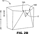
図1は、取付構造14に取り付けられた、2つのチップを備えたイオンビームミリングされたダイヤモンド12を含む工具10の平面図である。取付構造14は工具シャンクもしくはダイヤモンド12を保持するための他の金属製構造または複合物を備えている。ダイヤモンド12はろう付け、はんだ付け、接着剤、または1つ以上のボルトまたはねじなどの任意の他の固定機構により取付構造14内に固定することができる。取付構造14は、工具10を微細複製工具に溝または他の特徴群を切削するために用いるダイヤモンド工作機の装置に挿入可能な形状を有し得る。一例としてダイヤモンド工作機は、ダイヤモンドが移動するワークピースを通過してそのワークピースに溝を切削するプランジ研削用に構成されたダイヤモンド旋盤でもよい。代替的にはダイヤモンド工作機は、ダイヤモンドがワークピースに近接した軸を中心に回転してそのワークピース内に溝または他の特徴群を切削するフライカッティング用に構成されたダイヤモンド旋盤でもよい。
FIG. 1 is a plan view of a
ダイヤモンド12は多数のチップ16を画定する。各チップ16は、作製される微細複製工具の溝などのワークピースの個別の特徴群の形成に対応する別個の切削機構を画定する。図1に図示された実施形態においてダイヤモンド12は2つのチップ16Aおよび16Bを含むが、様々な実施形態用に対して任意の数のチップを形成し得る。チップ16Aおよび16Bは互いに隣接しているとともに、チップの間に谷17を形成している。集束イオンビームミリングプロセスを用いてチップ16Aおよび16Bを形成することができるとともに、効果的ダイヤモンド加工のために必要な特性を画定する谷17も形成し得る。例えば集束イオンビームミリングを用いてチップ16Aおよび16Bの内面18Aおよび18Bを共通軸19に沿って接するようにして谷17の底を形成することができる。また集束イオンビームミリングを用いて、凹状または凸状円弧楕円、放物線、数学的画定表面パターン、もしくはランダムまたは擬似ランダムパターンなどの特徴群を谷17内に形成することができる。
Diamond 12 defines a number of tips 16. Each tip 16 defines a separate cutting mechanism that corresponds to the formation of individual features of the workpiece, such as the grooves of the microreplicated tool being produced. In the embodiment illustrated in FIG. 1,
谷17が微細複製工具に形成される突起を画定できるため、谷17を高精細に作製することは非常に重要であり得る。例えば谷17は外部基準点に対して画定された半径を有する凹状または凸状円弧を画定し、または隣接表面18Aおよび18Bの間の角度を画定し得る。谷17の多様な他の形状も形成可能である。いずれの場合も微細複製工具内に作製された溝および突起は、微細複製工具が微細複製構造を形成する際に有効であるように精密な仕様と一致する必要がある。さらに多数のチップ16を単一ダイヤモンド上に形成するため、単一工具内で別個のダイヤモンドを使用することに関連する位置合わせ問題が回避できる。
Because the
図2Aおよび2Bは、本発明の一実施形態に係る、2つのチップを備えたイオンビームミリングされたダイヤモンド12の斜視図である。図示のようにダイヤモンド12は厚さXを画定し得る。谷17の底は厚さXに沿って実質距離Y延在し得る。YはX以下であり得る。図示のようにダイヤモンド12の上面は距離Yに沿って先細りになっているか、代替的には一定の高さを画定し得る。一例として厚さXはおよそ0.5ミリメートルと2ミリメートルの間であり、距離Yはおよそ0.001ミリメートルと0.5ミリメートルの間であり得るが、本発明は必ずしもこれらに限定されない。
2A and 2B are perspective views of ion beam milled
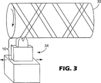
図3は、微細複製工具32の作製時に2つの溝を同時に切削するのに用いられる、2つのチップを備えた2チップダイヤモンド工具10の概念斜視図である。図3の例では微細複製工具32はキャスティングロールを含んでいるが、キャスティング・ベルト、射出成形用金型、押出または型押工具、もしくは他のワークピースなどにおける他の微細複製工具もダイヤモンド工具10を用いて作製することができる。ダイヤモンド工具10はダイヤモンド工作機34に固定可能であり、ダイヤモンド工作機34は微細複製工具32に対してダイヤモンド工具10を位置付けして、ダイヤモンド工具10を例えば微細複製工具32に対して横方向(矢印で示すように)に移動させる。同時に微細複製工具32は軸を中心に回転可能である。ダイヤモンド工作機34は、プランジャまたはねじ切り技術によりダイヤモンド工具10を回転微細複製工具32内に通過させて微細複製工具32内に溝を切削するように構成し得る。代替的にはダイヤモンド工作機34は、ダイヤモンド工具10が微細複製工具32に近接した軸を中心に回転して微細複製工具32に溝または他の特徴群を切削するフライカッティング用に構成し得る。またダイヤモンド工作機34はスクライビングまたは刻線用に構成可能であり、その場合ダイヤモンド工具10はワークピース全体に非常にゆっくりと移動させられる。いずれの場合も溝を切削可能であるとともに、ワークピース上に突起を形成可能である。形成された溝および突起は、例えば押出しプロセス時に微細複製工具32を用いて形成した微細複製構造の最終形状を画定し得る。代替的には、形成された溝および突起は、微細複製工具以外のワークピース内の材料の移動により特徴群を形成し得る。
FIG. 3 is a conceptual perspective view of a two-
ダイヤモンド工具10は多数のチップを有するダイヤモンドを実施するため、微細複製工具上に溝を切削するために必要なダイヤモンド工具の通過は少なくて済む。これにより生産コストが削減できると共に微細複製工具の作製に関連する生産サイクルを高速化することができる。ワークピースの製作には、場合によっては数日とまではいかなくても時間がかかることがある。同時使用のために2つ以上のチップをダイヤモンド工具10に組込むことにより生産サイクルをその時間の何分の一かに削減することができる。例えばダイヤモンドが2つのチップ16(図3に図示されているような)を含む場合には、微細複製工具32に溝を切削するのに必要な通過回数を、1つのチップを備えた1チップダイヤモンドを含むダイヤモンド工具と比べて2分の1削減できる。追加のチップ16は同様にさらなる利点を追加し得る。また同じダイヤモンドが微細複製工具32内に切削される多数の溝を画定するため、微細複製工具32内の個別切削溝間のばらつきを減少でき、微細複製工具32の品質を向上できる。品質を向上させることおよび微細複製工具32の作製に関連するコストを削減することが、ひいては微細複製構造の最終作製に関連するコストを効果的に削減し得る。
Since the
対照的に、1チップダイヤモンドを用いて微細複製工具上に溝を形成する場合、隣接溝間に深さのばらつきが生じ得る。深さの差は「クリーンアップ」と呼ばれることがあるが、これは溝の深さと微細複製工具上に形成された突起の高さとを調整するために微細複製工具への更なる変更が必要となる場合があるためである。このクリーンアップはマルチチップダイヤモンドを用いると低減または回避できる。この場合微細複製工具に形成された隣接溝の深さはマルチチップダイヤモンドの隣接するチップにより画定し得る。このため隣接するチップの高さを実質的に同一に画定すれば、微細複製工具に形成される隣接する溝の深さも同一になり得る。クリーンアップを防止または回避することで微細複製構造の形成に関連する時間及びコストも削減できる。 In contrast, when grooves are formed on a microreplication tool using one chip diamond, depth variations can occur between adjacent grooves. The depth difference is sometimes referred to as “cleanup”, which requires further changes to the microreplication tool to adjust the groove depth and the height of the protrusions formed on the microreplication tool. This is because there may be cases. This cleanup can be reduced or avoided using multi-chip diamond. In this case, the depth of adjacent grooves formed in the microreplication tool can be defined by adjacent chips of multichip diamond. For this reason, if the heights of adjacent chips are defined to be substantially the same, the depths of adjacent grooves formed in the microreplication tool can be the same. Preventing or avoiding cleanup can also reduce the time and cost associated with forming a microreplicated structure.
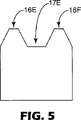
図4〜図7は、本発明の様々な実施形態に係る、2つのチップを備えたイオンビームミリングされたダイヤモンドの平面図である。図4〜図7の例により理解できるように、チップを多様な形状および大きさのいずれかを有するように形成し得る。例えば図4に示すように、チップ16Cおよび16Dは実質的矩形形状を画定し得る。この場合、谷17Cの底部はチップ16Cおよび16Dの上面と平行な平坦面になり得る。代替的には、谷17Cは凹状または凸状円弧などの非平坦面を画定し得る。
4-7 are plan views of ion beam milled diamond with two tips, according to various embodiments of the present invention. As can be understood from the examples of FIGS. 4-7, the chip can be formed to have any of a variety of shapes and sizes. For example, as shown in FIG. 4, the
図5に示すように、チップ16Eおよび16Fは平坦な上部を備えた先細形状を画定し得る。この場合、チップ16Eおよび16Fにより画定される側壁は、チップ16Eおよび16Fが平坦上部を備えたピラミッド様形状を画定するように先細になり得る。谷17Eの底部もチップ16Eおよび16Fの上面と平行な平坦面になり得る。代替的には、谷17Eの底部またはチップ16Eおよび16Fの上部は非平坦になり得る。
As shown in FIG. 5,
図6に示すように、チップ16Gおよび16Hはアンダーカット側壁を画定する。換言すれば、隣接するチップ16Gおよび16Hにより形成された谷17Gの底部は、谷17Gの底部に隣接する側面に対して鋭角を画定する。チップ16のこれらまたは他の構成は様々な用途に対して望ましい。
As shown in FIG. 6,
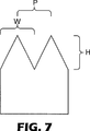
チップ16は多様な大きさも取り得る。チップの大きさは図7に図示するように、高さ(H)、幅(W)、およびピッチ(P)を含む1つ以上の変数により画定し得る。高さ(H)は谷の底部からチップの上部までの最大距離を指す。幅(W)は平均幅として、または図7に符号表示するようにチップの最大幅として画定し得る。ピッチ(P)は隣接チップ間の距離を指す。チップの大きさを画定するのに用いることができる他の数量はアスペクト比という。アスペクト比は幅(W)対高さ(H)の比である。集束イオンビームミリングプロセスにより作製した実験的なダイヤモンド工具は様々な高さ、幅、ピッチおよびアスペクト比の達成を立証した。 The chip 16 can take various sizes. The chip size may be defined by one or more variables including height (H), width (W), and pitch (P), as illustrated in FIG. Height (H) refers to the maximum distance from the bottom of the valley to the top of the chip. The width (W) may be defined as the average width or as the maximum width of the chip as indicated in FIG. Pitch (P) refers to the distance between adjacent chips. Another quantity that can be used to define chip size is called aspect ratio. The aspect ratio is the ratio of width (W) to height (H). Experimental diamond tools made by the focused ion beam milling process have demonstrated the achievement of various heights, widths, pitches and aspect ratios.
例えば高さ(H)および/または幅(W)は、およそ500マイクロメートル未満、およそ200マイクロメートル未満、およそ100マイクロメートル未満、およそ50マイクロメートル未満、およそ10マイクロメートル未満、およそ1.0マイクロメートル未満、またはおよそ0.1マイクロメートル未満に形成可能である。加えてピッチは、およそ500マイクロメートル未満、およそ200マイクロメートル未満、およそ100マイクロメートル未満、およそ50マイクロメートル未満、およそ10マイクロメートル未満、およそ1.0マイクロメートル未満、またはおよそ0.1マイクロメートル未満に画定可能である。アスペクト比はおよそ1:5超、およそ1:2超、およそ1:1超、およそ2:1超、またはおよそ5:1超に設定可能である。集束イオンビームミリングを用いてより大きなまたは小さなアスペクト比も達成し得る。これらの異なる形状および大きさは様々な用途にとって有利である。 For example, the height (H) and / or width (W) may be less than about 500 micrometers, less than about 200 micrometers, less than about 100 micrometers, less than about 50 micrometers, less than about 10 micrometers , about 1.0 micrometers. It can be formed to be less than a meter , or approximately less than 0.1 micrometers . In addition, the pitch is less than about 500 micrometers, less than about 200 micrometers, less than about 100 micrometers, less than about 50 micrometers, less than about 10 micrometers, less than about 1.0 micrometers , or about 0.1 micrometers. Can be defined below. The aspect ratio can be set to about 1: 5, about 1: 2, about 1: 1, about 2: 1, or about 5: 1. Larger or smaller aspect ratios may also be achieved using focused ion beam milling. These different shapes and sizes are advantageous for various applications.
集束イオンビームミリングは、ガリウムイオンなどのイオンがダイヤモンドに向けて加速されてダイヤモンドの原子を粉砕除去する(アブレーションという場合もある)プロセスを指す。ガリウムイオンの加速により、ダイヤモンドから原子を原子ごとに除去し得る。水蒸気を用いる蒸気強化技術を用いても、集束イオンビームミリングプロセスを向上し得る。1つの好適な集束イオンビームミリング機は、オレゴン州、ポートランド(Portland,Oregon)のFEIインコーポレイテッドから入手可能なミクリオン(Micrion)モデル9500である。本発明の原理によれば、集束イオンビームミリングプロセスを用いてマルチチップダイヤモンドを作製できることが実験的に分かっている。一般に、微細複製工具内に作製される特徴群を画定できる。そして集束イオンビームミリングを行うことにより形成される特徴群に相当する多数のチップを有するダイヤモンドを作製することができる。 Focused ion beam milling refers to a process in which ions such as gallium ions are accelerated toward diamond to crush and remove diamond atoms (sometimes called ablation). By acceleration of gallium ions, atoms can be removed from the diamond atom by atom. A steam enhancement technique using water vapor can also be used to improve the focused ion beam milling process. One suitable focused ion beam milling machine is a Miclion model 9500 available from FEI Incorporated, Portland, Oregon. In accordance with the principles of the present invention, it has been experimentally found that multi-chip diamond can be made using a focused ion beam milling process. In general, features created in the microreplication tool can be defined. Then, diamond having a large number of chips corresponding to the feature group formed by performing focused ion beam milling can be produced.
多数のチップを有するイオンビームミリングされたダイヤモンドを作製するために、微細複製工具に形成される特徴群が画定可能であるとともに、ダイヤモンドに対する仕様が作成可能である。仕様は、微細複製工具に形成される特徴群に相当する多数のチップを規定するものである。そして仕様を用いて集束イオンビームミリングを行うことにより仕様に応じたダイヤモンドを作製することができる。1つ以上のイオンビームミリングされたダイヤモンドを作製するのに利用し得る集束イオンビームミリングサービスの1つの代表的な供給会社は、ノースカロライナ州、ローリーのマテリアルズ・アナリティカル・サービス(Materials Analytical Services(Raleigh,North Carolina))である。 In order to produce ion beam milled diamond with multiple tips, the features formed on the microreplication tool can be defined and specifications for the diamond can be created. The specification defines a large number of chips corresponding to a group of features formed in the fine replication tool. Then, by performing focused ion beam milling using the specifications, diamond according to the specifications can be produced. One representative supplier of focused ion beam milling services that can be used to make one or more ion beam milled diamonds is Materials Analytical Services (Materials Analytical Services, Raleigh, NC). Raleigh, North Carolina)).
集束イオンビームミリングは一般に非常に高価である。そのためマルチチップダイヤモンドの作製に関連するコストを削減するために、イオンビームミリングされるダイヤモンドを集束イオンビームミリングにかける前に初期処理することが望ましい。例えばラッピング、グラインディング、またはワイヤソーイング技術などの安価な技術を用いてダイヤモンドの大部分を粉砕除去し得る。集束イオンビームミリングプロセスは、上記に列記した寸法または特徴のうちの1つ以上を達成するために必要となり得る。さらにダイヤモンドを集束イオンビームミリングの前に初期処理することにより、最終イオンビームミリングされたダイヤモンドを作製するのに必要な集束イオンビームミリング時間量を削減することができる。ラッピングは遊離砥粒を用いてダイヤモンドから材料を除去するプロセスを指し、一方グラインディングは媒体または基体に固定された研磨剤を用いてダイヤモンドから材料を除去するプロセスを指す。 Focused ion beam milling is generally very expensive. Therefore, it is desirable to initially treat the diamond to be ion beam milled before it is subjected to focused ion beam milling in order to reduce the costs associated with the production of multi-chip diamond. For example, most of the diamond can be crushed away using inexpensive techniques such as lapping, grinding, or wire sawing techniques. A focused ion beam milling process may be required to achieve one or more of the dimensions or features listed above. In addition, initial processing of diamond prior to focused ion beam milling can reduce the amount of focused ion beam milling time required to produce the final ion beam milled diamond. Lapping refers to the process of removing material from diamond using loose abrasive grains, while grinding refers to the process of removing material from diamond using an abrasive fixed to a medium or substrate.
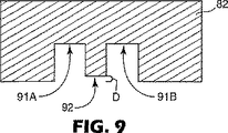
図8はワークピース82内に溝を切削している2チップダイヤモンド80を図示する断面平面図である。図9は、図8に図示された切削から得られた溝91Aおよび91Bならびに突起92を図示するワークピース82の他の断面平面図である。図8および図9により理解できるように、突起92は、ダイヤモンド80の隣接するチップ間に形成された谷により画定される。この理由で、突起92はワークピース82の外面から距離(D)離れることができる。つまり距離Dに相当する材料量をワークピースから除去して突起92の上部を画定する。これが1チップダイヤモンドを用いて作製した突起に比べて、ワークピース82上に形成された突起間のより高い均一性につながる。加えて突起92のクリーンアップを減少または回避し得る。
FIG. 8 is a cross-sectional plan view illustrating a two-
溝91Aおよび91Bも互いに対して実質的に同じ深さを有する。対照的に、1チップダイヤモンドを用いてダイヤモンド工具に溝を形成すると、隣接溝間の深さのばらつきが生じる恐れがある。マルチチップダイヤモンドを用いて同時に溝を切削することにより、隣接する溝間の深さのばらつきに関連するクリーンアップも減少または回避し得る。
図10および図11は、ワークピース82内に連続的に溝を切削している2チップダイヤモンド80(図10)、および切削の結果得られた溝および突起(図11)を図示するさらなる断面平面図である。つまり図10に図示された切削は図8に図示された切削後のものであり得る。図11に示すように、突起102に関連するクリーンアップは、距離Dの範囲が必要である。しかし他の突起92および104上のクリーンアップは減少または回避し得る。また突起92および104はワークピース82により同様に画定されるため、突起102に必要なクリーンアップ量は距離Dによってより容易に定量化できるが、距離Dはダイヤモンド80による各切削時に突起92および104の上部から除去された同一材料量に相当する。簡単に言うと、マルチチップダイヤモンドを用いることにより、ワークピース82により精細な特徴群を形成できるとともにクリーンアップの必要量を低減し得る。
10 and 11 are further cross-sectional planes illustrating the two-chip diamond 80 (FIG. 10) continuously cutting grooves in the
図12は、図10に図示された切削技術の変更例を図示する。図12は図8に図示したものに続いて切削を行う2チップダイヤモンド80を図示する断面平面図である。しかし図12では、後の切削は前の切削と重複する。換言すれば、ダイヤモンド80の左端のチップは溝92(図9)に従い、ダイヤモンド80の右端のチップが他の溝を切削する。このような切削技術はワークピース内の作製特徴群間により精細な類似性をもたらし、クリーンアップを減少または回避し得る。場合によってはダイヤモンド上により多数のチップを形成し得るが、後続切削通過時に1つのチップのみが重複し得る。重複チップを用いてワークピースに対してダイヤモンドを正確に位置付けし得るため、ワークピースに切削される特徴群は高さおよび深さの点でかなりの類似性を有する。
FIG. 12 illustrates a modification of the cutting technique illustrated in FIG. FIG. 12 is a cross-sectional plan view illustrating a two-
図13は、2チップダイヤモンドの作製を単純化するために用い得る一技術を図示する。ダイヤモンド130は、刃稜131Aおよび131Bをラッピングすることにより初期処理可能である。またワイヤソーを用いても初期谷132を形成できる。これらの単純な処理ステップは集束イオンビームミリングされたダイヤモンドを作製するのに必要な集束イオンビームミリング時間量を大幅に削減できる。一旦処理すれば、ダイヤモンド130を集束イオンビームミリングプロセスに送ることができる(図13の矢印により概念的に示されているように)。集束イオンビームミリングプロセスを用いてダイヤモンド130に対してガリウムイオンを加速することにより、ダイヤモンド原子を粉砕除去し、最終的にマルチチップイオンビームミリングされたダイヤモンド10を画定することができる。
FIG. 13 illustrates one technique that can be used to simplify the fabrication of two-chip diamonds. The
上記に概説したようにマルチチップダイヤモンドは任意の数のチップを含み、これらのチップは多様な形状および大きさを呈し得る。図14は、マルチチップダイヤモンドを図示する平面図である。図14の例ではマルチチップダイヤモンド140は9個の別個のチップを画定している。図14に図示したようなダイヤモンドのチップはおよそ0.1マイクロメートルの幅(W)、およそ0.2マイクロメートルのピッチ(P)、およそ0.2マイクロメートルの高さ(H)およびおよそ2:1のアスペクト比(H:W)を画定し得る。図2の図示と同様に、ダイヤモンド140は厚さ方向にある距離延在するとともに、ダイヤモンドの谷も厚さ方向にある距離延在し得る。
As outlined above, a multi-chip diamond includes any number of chips, and these chips can take on a variety of shapes and sizes. FIG. 14 is a plan view illustrating a multi-chip diamond. In the example of FIG. 14, the
図15は、図14に図示したようなマルチチップダイヤモンドの作製を単純化するために用い得る技術を図示する。この場合ダイヤモンド150は、側部151Aおよび151Bをラッピングまたはグラインディングによって初期処理可能であり、それにより1つの比較的幅広い突起152が画定される。一旦処理すれば、ダイヤモンド150を集束イオンビームミリングプロセスに送ることができる(図15の矢印により概念的に示されているように)。そして集束イオンビームミリングプロセスを適用してダイヤモンド150に対してガリウムイオンを加速することによりダイヤモンド原子を粉砕除去し、最終的に仕様に応じたマルチチップイオンビームミリングされたダイヤモンド140を画定することができる。
FIG. 15 illustrates a technique that can be used to simplify the production of multi-chip diamonds as illustrated in FIG. In this case, the
図16は、図2Bと同様な2つのチップを備えるイオンビームミリングされたダイヤモンドの斜視図である。図16に示すように、ダイヤモンド12は5つの特定表面(S1〜S5)を画定し得る。表面S1、S2およびS3はグラインディングまたはラッピング技術により形成可能であり、表面S4およびS5は集束イオンビームミリング技術により形成可能である。
FIG. 16 is a perspective view of an ion beam milled diamond with two tips similar to FIG. 2B. As shown in FIG. 16, the
図17〜図24は、本発明の様々な実施形態による様々なマルチチップイオンビームミリングされたダイヤモンドを図示する追加断面平面図である。図17に示すように、ダイヤモンドは異なる形状および大きさのチップを含み得る。例えばチップ171を用いてワークピースに1つのタイプの特徴群を形成し、チップ172を用いてワークピースに他のタイプの特徴群を形成することができる。一例として、チップ171の高さは、チップ172の高さのおよそ5倍超、およそ10倍超、またはおよそ20倍超に大きくすることができる。
17-24 are additional cross-sectional plan views illustrating various multi-chip ion beam milled diamonds according to various embodiments of the present invention. As shown in FIG. 17, the diamond may include chips of different shapes and sizes. For example, the
図18に示すように、ダイヤモンドは比較的小さいチップ182により離間した多数の比較的大きいチップ181Aおよび181Bを含み得る。この例では、チップ182は周期的正弦状関数を画定する。同様に図19に示すように、チップ191は周期的正弦状関数を画定し得る。任意の他の数学的関数、ランダムまたは擬似ランダム表面も形成し得る。図20は、2つのチップを備えるダイヤモンドの若干の変形を示し、チップ201の外面203が内面202の角度とは異なる角度を画定している。
As shown in FIG. 18, the diamond may include a number of relatively
図21は、チップ211がチップ212の側部上に形成されたダイヤモンドを図示する。図22は、チップ221および222が可変の異なる高さを画定するダイヤモンドを図示する。可変の谷、可変の内壁角度、および/または隣接チップ間の可変のピッチ間隔も画定し得る。
FIG. 21 illustrates a diamond with a
図23は、チップが凸半径(R)を有する谷を画定するダイヤモンドを図示する。図24は、多数の周期的正弦状チップがダイヤモンドの円弧形状表面に沿っているダイヤモンドを図示する。本発明のこれらおよび多数の他の変形例は請求の範囲内にある。 FIG. 23 illustrates a diamond where the tip defines a trough having a convex radius (R). FIG. 24 illustrates a diamond with a number of periodic sinusoidal tips along the arcuate surface of the diamond. These and many other variations of the invention are within the scope of the claims.
多数の実施形態を説明してきた。例えばマルチチップイオンビームミリングされたダイヤモンドをダイヤモンド工作機で用いるための説明をした。それにもかかわらず以下の請求項の範囲から逸脱することなく様々な変更を上述の実施形態に対して行うことが可能である。例えばマルチチップダイヤモンドを用いて他のタイプのワークピース、例えば微細複製工具以外のワークピースに溝または他の特徴群を切削し得る。したがって他の実施および実施形態は、特許請求の範囲内にある。 A number of embodiments have been described. For example, the explanation was given for using diamond subjected to multi-chip ion beam milling in a diamond machine tool. Nevertheless, various modifications can be made to the above-described embodiments without departing from the scope of the following claims. For example, multi-chip diamond can be used to cut grooves or other features in other types of workpieces, eg, workpieces other than microreplication tools. Accordingly, other implementations and embodiments are within the scope of the claims.
Claims (4)
前記微細複製工具に形成される構造群に相当する複数のチップを規定する、ダイヤモンドの仕様を作成するステップと、
前記ダイヤモンドが複数のチップを有するように、前記仕様を用いて前記ダイヤモンドを集束イオンビームミリングするステップと、
前記集束イオンビームミリングされたダイヤモンドを用いて微細複製工具を作製するステップと、を含み、
前記微細複製工具を作製するステップが、前記集束イオンビームミリングされたダイヤモンドの複数回の通過により前記微細複製工具に複数の溝を切削するステップを含み、前記溝の数が前記ダイヤモンドの通過の回数より大きい、
方法。 Defining a group of structures formed in a microreplication tool used to create a microreplication structure ;
Creating a diamond specification defining a plurality of chips corresponding to a structure group formed in the microreplication tool;
Focused ion beam milling of the diamond using the specifications such that the diamond has a plurality of tips;
Using the focused ion beam milled diamond to produce a microreplication tool,
Producing the microreplication tool includes cutting a plurality of grooves in the microreplication tool by a plurality of passes of the focused ion beam milled diamond, wherein the number of grooves is the number of passes of the diamond. Greater than,
Method.
Applications Claiming Priority (3)
| Application Number | Priority Date | Filing Date | Title |
|---|---|---|---|
| US10/159,925 | 2002-05-29 | ||
| US10/159,925 US7140812B2 (en) | 2002-05-29 | 2002-05-29 | Diamond tool with a multi-tipped diamond |
| PCT/US2003/011204 WO2003101704A1 (en) | 2002-05-29 | 2003-04-10 | Diamond tool with a multi-tipped diamond |
Publications (3)
| Publication Number | Publication Date |
|---|---|
| JP2005527394A JP2005527394A (en) | 2005-09-15 |
| JP2005527394A5 JP2005527394A5 (en) | 2006-06-01 |
| JP4943649B2 true JP4943649B2 (en) | 2012-05-30 |
Family
ID=29583060
Family Applications (1)
| Application Number | Title | Priority Date | Filing Date |
|---|---|---|---|
| JP2004509032A Expired - Fee Related JP4943649B2 (en) | 2002-05-29 | 2003-04-10 | Diamond tool with multi-chip diamond |
Country Status (11)
| Country | Link |
|---|---|
| US (2) | US7140812B2 (en) |
| EP (1) | EP1507643B1 (en) |
| JP (1) | JP4943649B2 (en) |
| KR (1) | KR100960754B1 (en) |
| CN (1) | CN100548632C (en) |
| AT (1) | ATE517732T1 (en) |
| AU (1) | AU2003223567A1 (en) |
| BR (1) | BR0311289A (en) |
| CA (1) | CA2487366A1 (en) |
| MX (1) | MXPA04011830A (en) |
| WO (1) | WO2003101704A1 (en) |
Families Citing this family (77)
| Publication number | Priority date | Publication date | Assignee | Title |
|---|---|---|---|---|
| JP4556383B2 (en) * | 2002-11-29 | 2010-10-06 | コニカミノルタホールディングス株式会社 | Processing method of transfer optical surface |
| US7224529B2 (en) * | 2003-09-09 | 2007-05-29 | 3M Innovative Properties Company | Microreplicated article |
| US7804649B2 (en) * | 2003-09-09 | 2010-09-28 | 3M Innovative Properties Company | Microreplicated achromatic lens |
| US7165959B2 (en) * | 2003-09-09 | 2007-01-23 | 3M Innovative Properties Company | Apparatus and method for producing two-sided patterned webs in registration |
| US20050231809A1 (en) * | 2003-09-09 | 2005-10-20 | Carlson Daniel H | Microreplicated polarizing article |
| US7160583B2 (en) | 2004-12-03 | 2007-01-09 | 3M Innovative Properties Company | Microfabrication using patterned topography and self-assembled monolayers |
| EP1863594B1 (en) * | 2005-03-09 | 2011-01-26 | 3M Innovative Properties Company | Apparatus and method for making microreplicated article |
| MX2007010905A (en) * | 2005-03-09 | 2007-12-07 | 3M Innovative Properties Co | Microreplicated article with defect-reducing surface. |
| BRPI0608701A2 (en) * | 2005-03-09 | 2010-01-19 | 3M Innovative Properties Co | micro-replicated article and method of making a micro-replicated article |
| WO2006098935A1 (en) * | 2005-03-09 | 2006-09-21 | 3M Innovative Properties Company | Apparatus and method for producing two-sided patterned web in registration |
| CN101137493B (en) * | 2005-03-09 | 2012-04-11 | 3M创新有限公司 | Apparatus and method for making microreplicated article |
| MX2007010903A (en) * | 2005-03-09 | 2007-12-05 | 3M Innovative Properties Co | Microreplicated article with moire reducing surface. |
| US8709219B2 (en) * | 2005-03-10 | 2014-04-29 | Panasonic Corporation | Structured diamond tool made by focused ion beam nanomachining |
| US7445409B2 (en) * | 2005-10-19 | 2008-11-04 | 3M Innovative Properties Company | Cutting tool assembly including diamond cutting tips at half-pitch spacing for land feature creation |
| US7757591B2 (en) * | 2005-10-19 | 2010-07-20 | 3M Innovative Properties Company | Aligned multi-diamond cutting tool assembly for creating microreplication tools |
| US7614831B2 (en) * | 2006-03-13 | 2009-11-10 | Panasonic Corporation | Machining tools having concave cutting surfaces for precision machining and methods of manufacturing such |
| US7677146B2 (en) * | 2006-05-10 | 2010-03-16 | 3M Innovative Properties Company | Cutting tool using one or more machined tool tips in a continuous or interrupted cut fast tool servo |
| US7628100B2 (en) * | 2007-01-05 | 2009-12-08 | 3M Innovative Properties Company | Cutting tool using one or more machined tool tips with diffractive features in a continuous or interrupted cut fast tool servo |
| TW200920521A (en) | 2007-04-05 | 2009-05-16 | Toshiba Machine Co Ltd | Method and apparatus for machining surface of roll |
| US9180524B2 (en) | 2007-08-06 | 2015-11-10 | 3M Innovative Properties Company | Fly-cutting head, system and method, and tooling and sheeting produced therewith |
| US20090041553A1 (en) * | 2007-08-06 | 2009-02-12 | 3M Innovative Properties Company | Fly-cutting system and method, and related tooling and articles |
| US7669508B2 (en) * | 2007-10-29 | 2010-03-02 | 3M Innovative Properties Company | Cutting tool using one or more machined tool tips with diffractive features |
| US20090147361A1 (en) * | 2007-12-07 | 2009-06-11 | 3M Innovative Properties Company | Microreplicated films having diffractive features on macro-scale features |
| JP5827120B2 (en) | 2008-04-02 | 2015-12-02 | スリーエム イノベイティブ プロパティズ カンパニー | Light guide film and method for producing light guide film |
| TW200946975A (en) * | 2008-04-02 | 2009-11-16 | 3M Innovative Properties Co | Methods and systems for fabricating optical films having superimposed features |
| DE102008058452A1 (en) | 2008-08-05 | 2010-02-11 | Gühring Ohg | Method and tool for producing a surface of predetermined roughness |
| JP2010115741A (en) * | 2008-11-12 | 2010-05-27 | Toshiba Mach Co Ltd | Cutting method of high hardness material and cutting machine |
| CN102458728A (en) * | 2009-05-04 | 2012-05-16 | 3M创新有限公司 | Methods for making microreplication tools |
| WO2011130151A1 (en) | 2010-04-12 | 2011-10-20 | 3M Innovative Properties Company | Optical stack and lightguides |
| DE102010028625A1 (en) * | 2010-05-05 | 2011-11-10 | Komet Group Gmbh | Tool carrier with cutting tool for turning |
| EP2404739A1 (en) | 2010-07-09 | 2012-01-11 | 3M Innovative Properties Co. | Durable hyrophobic structured surface |
| EP2632613B1 (en) | 2010-10-28 | 2017-08-30 | 3M Innovative Properties Company | Engineered surfaces for reducing bacterial adhesion |
| US8692446B2 (en) | 2011-03-17 | 2014-04-08 | 3M Innovative Properties Company | OLED light extraction films having nanoparticles and periodic structures |
| TWI453107B (en) * | 2011-07-11 | 2014-09-21 | Benq Materials Corp | Manufacturing method of roller used for manufacturing patterned retardation film |
| US8659221B2 (en) | 2011-08-26 | 2014-02-25 | 3M Innovative Properties Company | OLED light extraction film with multi-periodic zones of nanostructures |
| CN102431367B (en) * | 2011-08-31 | 2014-07-02 | 明基材料有限公司 | Method for manufacturing roller of phase-difference film |
| JP5821483B2 (en) * | 2011-09-30 | 2015-11-24 | 大日本印刷株式会社 | Roll mold manufacturing method, roll mold, and optical sheet manufacturing method |
| CN102335763A (en) * | 2011-10-24 | 2012-02-01 | 山东蓝天首饰有限公司 | Cutter special for processing jewelry and method for using cutter |
| JP6290794B2 (en) | 2012-02-28 | 2018-03-07 | スリーエム イノベイティブ プロパティズ カンパニー | Composition comprising surface-modified high refractive index nanoparticles suitable for an optical coupling layer |
| JP5880206B2 (en) * | 2012-03-28 | 2016-03-08 | 大日本印刷株式会社 | Prism sheet mold manufacturing method |
| SE537354C2 (en) * | 2012-04-24 | 2015-04-14 | Sandvik Intellectual Property | Indexable cutter and tool for chip separating machining where the cutter has six equally long cutting tips, as well as the basic body for the tool |
| US9545024B2 (en) * | 2012-05-29 | 2017-01-10 | Apple Inc. | Diamond cutting tools |
| US9537116B2 (en) | 2012-08-22 | 2017-01-03 | 3M Innovative Properties Company | Transparent OLED light extraction |
| US20150228929A1 (en) | 2012-08-22 | 2015-08-13 | 3M Innovative Properties Company | Microcavity oled light extraction |
| US9050669B2 (en) | 2012-10-04 | 2015-06-09 | Illinois Tool Works Inc. | Rapidly retractable tool support for a pipe machining apparatus |
| KR20150091111A (en) | 2012-11-30 | 2015-08-07 | 쓰리엠 이노베이티브 프로퍼티즈 컴파니 | Emissive display with reflective polarizer |
| CN104823231B (en) | 2012-11-30 | 2017-06-23 | 3M创新有限公司 | Emission display with hybrid-type polarizer |
| US9610636B2 (en) | 2013-01-09 | 2017-04-04 | Illinois Tool Works Inc. | Pipe machining apparatuses and methods of operating the same |
| US9623484B2 (en) * | 2013-01-14 | 2017-04-18 | Illinois Tool Works Inc. | Pipe machining apparatuses and methods of operating the same |
| JP6107210B2 (en) * | 2013-02-20 | 2017-04-05 | 日本精工株式会社 | Thread part processing method and processing apparatus |
| WO2014189716A1 (en) | 2013-05-21 | 2014-11-27 | 3M Innovative Properties Company | Nanostructured spore carrier |
| EP3033778A4 (en) | 2013-08-12 | 2017-03-29 | 3M Innovative Properties Company | Emissive article with light extraction film |
| MX370557B (en) | 2013-10-03 | 2019-12-17 | Illinois Tool Works | Pivotal tool support for a pipe machining apparatus. |
| JP6949489B2 (en) | 2014-06-13 | 2021-10-13 | スリーエム イノベイティブ プロパティズ カンパニー | Optical stack for sparkle reduction |
| WO2015191339A1 (en) | 2014-06-13 | 2015-12-17 | 3M Innovative Properties Company | Optical stacks for sparkle reduction |
| JP6465367B2 (en) * | 2014-06-23 | 2019-02-06 | 住友電工ハードメタル株式会社 | Cutting tools |
| GB2528289A (en) | 2014-07-16 | 2016-01-20 | Kraft Foods R&D Inc | A die-cut lid and associated container and method |
| US9862124B2 (en) | 2014-07-18 | 2018-01-09 | 3M Innovative Properties Company | Multilayer optical adhesives and methods of making same |
| DE102014117398B3 (en) * | 2014-11-27 | 2016-05-25 | Thielenhaus Technologies Gmbh | Method for generating grooves on a camshaft |
| US10065246B2 (en) | 2015-04-13 | 2018-09-04 | Illinois Tool Works Inc. | Laser line generator tool for a pipe machining apparatus |
| EP3334552A4 (en) | 2015-08-12 | 2019-06-26 | Illinois Tool Works Inc. | Crash resistant trip for a pipe for a machining apparatus |
| CN105382663B (en) * | 2015-11-11 | 2017-08-08 | 沈阳黎明航空发动机(集团)有限责任公司 | A kind of processing method of diamond roller Surface inspection test piece |
| KR102567221B1 (en) | 2015-12-09 | 2023-08-16 | 매사추세츠 머티리얼즈 테크놀로지스 엘엘씨 | Measurement of material properties under local tensile stress through contact mechanics |
| JP2019501416A (en) | 2015-12-09 | 2019-01-17 | スリーエム イノベイティブ プロパティズ カンパニー | Optical laminate |
| US11708510B2 (en) | 2016-01-15 | 2023-07-25 | 3M Innovative Properties Company | Optical adhesive |
| US10512974B1 (en) | 2016-12-07 | 2019-12-24 | Quantum Valley Investment Fund LP | Diamond machining tool |
| US11583933B1 (en) * | 2017-01-19 | 2023-02-21 | Consolidated Nuclear Security, LLC | Shaped cutting tool and method of use to efficiently form a finished part |
| US10596633B1 (en) * | 2017-01-19 | 2020-03-24 | Consolidated Nuclear Security, LLC | Shaped cutting tool |
| US11378723B2 (en) | 2017-06-02 | 2022-07-05 | 3M Innovative Properties Company | Optical film and optical system |
| JP7106774B2 (en) * | 2017-06-21 | 2022-07-26 | デクセリアルズ株式会社 | Microfabrication device, microfabrication unit, control device, master manufacturing method, and microfabrication method for master substrate |
| DE102017121354A1 (en) * | 2017-09-14 | 2019-03-14 | Gühring KG | Roughening tool and method for its production |
| US11402637B2 (en) | 2018-04-20 | 2022-08-02 | 3M Innovative Properties Company | Headset and head-mounted display |
| EP3808208B1 (en) * | 2018-06-15 | 2023-10-25 | Lg Chem, Ltd. | Decoration member |
| US11766822B2 (en) | 2019-08-20 | 2023-09-26 | 3M Innovative Properties Company | Microstructured surface with increased microorganism removal when cleaned, articles and methods |
| WO2022243772A1 (en) | 2021-05-20 | 2022-11-24 | 3M Innovative Properties Company | Micro-cut patterned article and method of making same |
| WO2023105372A1 (en) | 2021-12-07 | 2023-06-15 | 3M Innovative Properties Company | Microstructured surface and articles with lower visibilty of scratches and methods |
| WO2024047419A1 (en) | 2022-08-31 | 2024-03-07 | Solventum Intellectual Properties Company | Articles including a microstructured curved surface, tooling articles, and methods |
Family Cites Families (41)
| Publication number | Priority date | Publication date | Assignee | Title |
|---|---|---|---|---|
| US2733730A (en) * | 1956-02-07 | turak | ||
| US1348115A (en) * | 1918-08-31 | 1920-07-27 | Leon G Buckwalter | Reversible-taper roughing-reamer |
| FR967169A (en) | 1948-05-18 | 1950-10-27 | One-piece phonograph needle or style, but two-piece of different flexibility and stiffness | |
| DE885163C (en) | 1951-06-16 | 1953-08-03 | Blaupunkt Elektronik G M B H | Universal double needles for normal and micro-groove records |
| US2738730A (en) * | 1952-07-01 | 1956-03-20 | Fairchild Camera Instr Co | Method for forming engraved image-reproducing plates |
| CH359899A (en) | 1959-07-24 | 1962-01-31 | Colomb Andre | A method of manufacturing a sapphire needle for a speaking machine and a needle obtained by implementing this method |
| US3680213A (en) * | 1969-02-03 | 1972-08-01 | Karl O Reichert | Method of grooving semiconductor wafer for the dividing thereof |
| US3780409A (en) * | 1971-02-19 | 1973-12-25 | Fansteel Inc | Threading tool |
| US3813970A (en) * | 1972-01-10 | 1974-06-04 | Ammco Tools Inc | Tool holder |
| US3893356A (en) * | 1974-03-19 | 1975-07-08 | Frank Atzberger | Rotor cutter |
| US4035590A (en) * | 1975-06-30 | 1977-07-12 | Rca Corporation | Apparatus for electromechanical recording of short wavelength modulation in a metal master |
| US4044379A (en) * | 1975-06-30 | 1977-08-23 | Rca Corporation | Method and apparatus for electromechanical recording of short wavelength modulation in a metal master |
| US4113267A (en) * | 1977-04-25 | 1978-09-12 | Pickering & Company, Inc. | Double stylus assembly for phonograph record stamper playback |
| US4113266A (en) | 1977-04-25 | 1978-09-12 | Pickering & Company, Inc. | Playback stylus for phonograph record stamper |
| US4111083A (en) * | 1977-08-08 | 1978-09-05 | Carter Walter L | Tool holder |
| US4287689A (en) * | 1979-10-30 | 1981-09-08 | Rca Corporation | Method for improving the quality of low frequency output of a video disc pickup stylus |
| US4355382A (en) * | 1980-12-24 | 1982-10-19 | Rca Corporation | Apparatus for sharpening a cutting stylus |
| JPS58177543A (en) * | 1982-04-09 | 1983-10-18 | Hitachi Ltd | Reproducing stylus for video disk and its manufacture |
| US4525751A (en) * | 1982-08-27 | 1985-06-25 | Rca Corporation | Disc record with tapered groove |
| DE3718262A1 (en) * | 1987-05-30 | 1988-12-08 | Werner Hermann Wera Werke | PUNCH KNIFE MILLING MACHINE |
| WO1989004052A1 (en) | 1987-10-22 | 1989-05-05 | Oxford Instruments Limited | Exposing substrates to ion beams |
| JPH0366501A (en) * | 1989-08-03 | 1991-03-22 | Kawasaki Steel Corp | Recessing method for plated roll surface |
| JPH0679504A (en) * | 1992-08-31 | 1994-03-22 | Sumitomo Electric Ind Ltd | Polycrystal diamond cutting tool and its manufacture |
| US6069080A (en) * | 1992-08-19 | 2000-05-30 | Rodel Holdings, Inc. | Fixed abrasive polishing system for the manufacture of semiconductor devices, memory disks and the like |
| US5216843A (en) * | 1992-09-24 | 1993-06-08 | Intel Corporation | Polishing pad conditioning apparatus for wafer planarization process |
| US5663802A (en) * | 1993-02-25 | 1997-09-02 | Ohio Electronic Engravers, Inc. | Method and apparatus for engraving using multiple engraving heads |
| SG64333A1 (en) * | 1993-09-13 | 1999-04-27 | Minnesota Mining & Mfg | Abrasive article method of manufacture of same method of using same for finishing and a production tool |
| US5555473A (en) * | 1995-02-21 | 1996-09-10 | Ohio Electronic Engravers, Inc. | Engraving system and method for helical or circumferential engraving |
| US5958799A (en) * | 1995-04-13 | 1999-09-28 | North Carolina State University | Method for water vapor enhanced charged-particle-beam machining |
| US5814355A (en) * | 1996-04-30 | 1998-09-29 | Minnesota Mining And Manufacturing Company | Mold for producing glittering cube-corner retroreflective sheeting |
| AU3786997A (en) * | 1996-07-30 | 1998-02-20 | Drukker International B.V. | A method of producing a cutting tool insert |
| NL1004016C2 (en) * | 1996-09-12 | 1998-03-13 | Oce Tech Bv | Inkjet print head. |
| US6253442B1 (en) * | 1997-07-02 | 2001-07-03 | 3M Innovative Properties Company | Retroreflective cube corner sheeting mold and method for making the same |
| US6077462A (en) * | 1998-02-20 | 2000-06-20 | 3M Innovative Properties Company | Method and apparatus for seamless microreplication using an expandable mold |
| JPH11267902A (en) * | 1998-03-23 | 1999-10-05 | Hiroshi Hashimoto | Tool having ultra-fine cutting blade and processing tool having ultra-fine cutting blade |
| DE19836771A1 (en) * | 1998-08-13 | 2000-02-17 | Backes Rudolf | Shaping process for producing grooves in hardened workpieces uses interchangeable tool plates whose engagement area is made from hard brittle material which breaks in event of excessive strain |
| JP3299523B2 (en) * | 1999-07-08 | 2002-07-08 | 東邦エンジニアリング株式会社 | Tool for turning groove of hard foam resin pad |
| IL138710A0 (en) | 1999-10-15 | 2001-10-31 | Newman Martin H | Atomically sharp edge cutting blades and method for making same |
| JP2001310204A (en) * | 2000-04-25 | 2001-11-06 | Toshiba Tungaloy Co Ltd | Throw-away tip and bite holder for grooving |
| US6578254B2 (en) * | 2000-12-08 | 2003-06-17 | Sandia Corporation | Damascene fabrication of nonplanar microcoils |
| JP2002307210A (en) * | 2001-04-19 | 2002-10-23 | Toyoda Van Moppes Ltd | Single crystal diamond cutting tool and its manufacturing method |
-
2002
- 2002-05-29 US US10/159,925 patent/US7140812B2/en not_active Expired - Lifetime
-
2003
- 2003-04-10 WO PCT/US2003/011204 patent/WO2003101704A1/en active Application Filing
- 2003-04-10 BR BR0311289-6A patent/BR0311289A/en not_active IP Right Cessation
- 2003-04-10 MX MXPA04011830A patent/MXPA04011830A/en active IP Right Grant
- 2003-04-10 JP JP2004509032A patent/JP4943649B2/en not_active Expired - Fee Related
- 2003-04-10 KR KR1020047019121A patent/KR100960754B1/en active IP Right Grant
- 2003-04-10 AT AT03719704T patent/ATE517732T1/en not_active IP Right Cessation
- 2003-04-10 CN CNB038120038A patent/CN100548632C/en not_active Expired - Lifetime
- 2003-04-10 AU AU2003223567A patent/AU2003223567A1/en not_active Abandoned
- 2003-04-10 EP EP03719704A patent/EP1507643B1/en not_active Expired - Lifetime
- 2003-04-10 CA CA002487366A patent/CA2487366A1/en not_active Abandoned
-
2006
- 2006-10-23 US US11/551,772 patent/US20070039433A1/en not_active Abandoned
Also Published As
| Publication number | Publication date |
|---|---|
| WO2003101704A1 (en) | 2003-12-11 |
| CA2487366A1 (en) | 2003-12-11 |
| US7140812B2 (en) | 2006-11-28 |
| CN1655920A (en) | 2005-08-17 |
| JP2005527394A (en) | 2005-09-15 |
| KR100960754B1 (en) | 2010-06-01 |
| EP1507643A1 (en) | 2005-02-23 |
| AU2003223567A1 (en) | 2003-12-19 |
| CN100548632C (en) | 2009-10-14 |
| BR0311289A (en) | 2005-04-26 |
| US20070039433A1 (en) | 2007-02-22 |
| ATE517732T1 (en) | 2011-08-15 |
| US20030223830A1 (en) | 2003-12-04 |
| KR20050005495A (en) | 2005-01-13 |
| EP1507643B1 (en) | 2011-07-27 |
| MXPA04011830A (en) | 2005-03-31 |
Similar Documents
| Publication | Publication Date | Title |
|---|---|---|
| JP4943649B2 (en) | Diamond tool with multi-chip diamond | |
| KR101046810B1 (en) | Multi-Diamond Cutting Tool Assembly for Microreplication Tool Generation | |
| KR101330857B1 (en) | Aligned multi-diamond cutting tool assembly for creating microreplication tools and method for creating the same | |
| JP2012525990A (en) | Manufacturing method of fine replication tool | |
| JP2909104B2 (en) | Cutter plate for precision machining and method of manufacturing the same | |
| US5981895A (en) | Method of manufacture of a bone saw blade by wire cutting electric discharge machining | |
| US20080156061A1 (en) | Method of producing honeycomb structure molding die | |
| WO2017213026A1 (en) | Micromachining method, die manufacturing method, and micromachining apparatus | |
| JP2017217720A5 (en) | ||
| JP2002192417A (en) | Grooving device, and grooving method using the same | |
| TW200539974A (en) | Cutting tool for simultaneous facing and grooving of CMP pad | |
| RU2184025C1 (en) | Method for dressing coaxially mounted end grinding discs | |
| JP2004188511A (en) | Method of fine groove working, workpiece with fine grooves, and molding | |
| JPH10244560A (en) | Injection mold and its production | |
| JP2001054819A (en) | Tip saw | |
| JPH02205401A (en) | Working method for fine groove | |
| JP2011110632A (en) | Surface processing method |
Legal Events
| Date | Code | Title | Description |
|---|---|---|---|
| A521 | Request for written amendment filed |
Free format text: JAPANESE INTERMEDIATE CODE: A523 Effective date: 20060405 |
|
| A621 | Written request for application examination |
Free format text: JAPANESE INTERMEDIATE CODE: A621 Effective date: 20060405 |
|
| A131 | Notification of reasons for refusal |
Free format text: JAPANESE INTERMEDIATE CODE: A131 Effective date: 20090106 |
|
| A601 | Written request for extension of time |
Free format text: JAPANESE INTERMEDIATE CODE: A601 Effective date: 20090403 |
|
| A602 | Written permission of extension of time |
Free format text: JAPANESE INTERMEDIATE CODE: A602 Effective date: 20090410 |
|
| A521 | Request for written amendment filed |
Free format text: JAPANESE INTERMEDIATE CODE: A523 Effective date: 20090626 |
|
| A131 | Notification of reasons for refusal |
Free format text: JAPANESE INTERMEDIATE CODE: A131 Effective date: 20090818 |
|
| A131 | Notification of reasons for refusal |
Free format text: JAPANESE INTERMEDIATE CODE: A131 Effective date: 20100119 |
|
| A601 | Written request for extension of time |
Free format text: JAPANESE INTERMEDIATE CODE: A601 Effective date: 20100416 |
|
| A602 | Written permission of extension of time |
Free format text: JAPANESE INTERMEDIATE CODE: A602 Effective date: 20100423 |
|
| A02 | Decision of refusal |
Free format text: JAPANESE INTERMEDIATE CODE: A02 Effective date: 20100907 |
|
| A601 | Written request for extension of time |
Free format text: JAPANESE INTERMEDIATE CODE: A601 Effective date: 20111206 |
|
| A602 | Written permission of extension of time |
Free format text: JAPANESE INTERMEDIATE CODE: A602 Effective date: 20111209 |
|
| A521 | Request for written amendment filed |
Free format text: JAPANESE INTERMEDIATE CODE: A523 Effective date: 20120106 |
|
| A01 | Written decision to grant a patent or to grant a registration (utility model) |
Free format text: JAPANESE INTERMEDIATE CODE: A01 |
|
| A61 | First payment of annual fees (during grant procedure) |
Free format text: JAPANESE INTERMEDIATE CODE: A61 Effective date: 20120301 |
|
| R150 | Certificate of patent or registration of utility model |
Free format text: JAPANESE INTERMEDIATE CODE: R150 Ref document number: 4943649 Country of ref document: JP Free format text: JAPANESE INTERMEDIATE CODE: R150 |
|
| FPAY | Renewal fee payment (event date is renewal date of database) |
Free format text: PAYMENT UNTIL: 20150309 Year of fee payment: 3 |
|
| R250 | Receipt of annual fees |
Free format text: JAPANESE INTERMEDIATE CODE: R250 |
|
| R250 | Receipt of annual fees |
Free format text: JAPANESE INTERMEDIATE CODE: R250 |
|
| R250 | Receipt of annual fees |
Free format text: JAPANESE INTERMEDIATE CODE: R250 |
|
| R250 | Receipt of annual fees |
Free format text: JAPANESE INTERMEDIATE CODE: R250 |
|
| R250 | Receipt of annual fees |
Free format text: JAPANESE INTERMEDIATE CODE: R250 |
|
| R250 | Receipt of annual fees |
Free format text: JAPANESE INTERMEDIATE CODE: R250 |
|
| R250 | Receipt of annual fees |
Free format text: JAPANESE INTERMEDIATE CODE: R250 |
|
| R250 | Receipt of annual fees |
Free format text: JAPANESE INTERMEDIATE CODE: R250 |
|
| LAPS | Cancellation because of no payment of annual fees |