JP4935525B2 - Method for manufacturing organic electroluminescence device - Google Patents
Method for manufacturing organic electroluminescence device Download PDFInfo
- Publication number
- JP4935525B2 JP4935525B2 JP2007160176A JP2007160176A JP4935525B2 JP 4935525 B2 JP4935525 B2 JP 4935525B2 JP 2007160176 A JP2007160176 A JP 2007160176A JP 2007160176 A JP2007160176 A JP 2007160176A JP 4935525 B2 JP4935525 B2 JP 4935525B2
- Authority
- JP
- Japan
- Prior art keywords
- ink
- light emitting
- printing
- organic
- organic light
- Prior art date
- Legal status (The legal status is an assumption and is not a legal conclusion. Google has not performed a legal analysis and makes no representation as to the accuracy of the status listed.)
- Expired - Fee Related
Links
- 238000000034 method Methods 0.000 title claims description 41
- 238000005401 electroluminescence Methods 0.000 title claims description 36
- 238000004519 manufacturing process Methods 0.000 title claims description 14
- 238000007639 printing Methods 0.000 claims description 87
- 239000000463 material Substances 0.000 claims description 60
- 238000007774 anilox coating Methods 0.000 claims description 41
- 239000002904 solvent Substances 0.000 claims description 31
- 239000000758 substrate Substances 0.000 claims description 28
- 238000012546 transfer Methods 0.000 claims description 19
- 239000011347 resin Substances 0.000 claims description 12
- 229920005989 resin Polymers 0.000 claims description 12
- 239000000976 ink Substances 0.000 description 111
- YXFVVABEGXRONW-UHFFFAOYSA-N Toluene Chemical compound CC1=CC=CC=C1 YXFVVABEGXRONW-UHFFFAOYSA-N 0.000 description 45
- CTQNGGLPUBDAKN-UHFFFAOYSA-N O-Xylene Chemical compound CC1=CC=CC=C1C CTQNGGLPUBDAKN-UHFFFAOYSA-N 0.000 description 23
- 238000001035 drying Methods 0.000 description 13
- 239000008096 xylene Substances 0.000 description 13
- 239000002635 aromatic organic solvent Substances 0.000 description 10
- 230000000052 comparative effect Effects 0.000 description 10
- 239000011521 glass Substances 0.000 description 10
- 229920001971 elastomer Polymers 0.000 description 9
- 230000005525 hole transport Effects 0.000 description 9
- 238000000576 coating method Methods 0.000 description 8
- PAYRUJLWNCNPSJ-UHFFFAOYSA-N Aniline Chemical compound NC1=CC=CC=C1 PAYRUJLWNCNPSJ-UHFFFAOYSA-N 0.000 description 6
- RDOXTESZEPMUJZ-UHFFFAOYSA-N anisole Chemical compound COC1=CC=CC=C1 RDOXTESZEPMUJZ-UHFFFAOYSA-N 0.000 description 6
- 230000015572 biosynthetic process Effects 0.000 description 6
- 238000007644 letterpress printing Methods 0.000 description 6
- 239000003960 organic solvent Substances 0.000 description 6
- 239000010409 thin film Substances 0.000 description 6
- 229940078552 o-xylene Drugs 0.000 description 5
- 229920000642 polymer Polymers 0.000 description 5
- 239000011248 coating agent Substances 0.000 description 4
- 239000007788 liquid Substances 0.000 description 4
- 239000013557 residual solvent Substances 0.000 description 4
- ZWEHNKRNPOVVGH-UHFFFAOYSA-N 2-Butanone Chemical compound CCC(C)=O ZWEHNKRNPOVVGH-UHFFFAOYSA-N 0.000 description 3
- CSCPPACGZOOCGX-UHFFFAOYSA-N Acetone Chemical compound CC(C)=O CSCPPACGZOOCGX-UHFFFAOYSA-N 0.000 description 3
- 229920001609 Poly(3,4-ethylenedioxythiophene) Polymers 0.000 description 3
- 239000002131 composite material Substances 0.000 description 3
- 239000010408 film Substances 0.000 description 3
- UZKWTJUDCOPSNM-UHFFFAOYSA-N methoxybenzene Substances CCCCOC=C UZKWTJUDCOPSNM-UHFFFAOYSA-N 0.000 description 3
- 239000000178 monomer Substances 0.000 description 3
- 238000007645 offset printing Methods 0.000 description 3
- 229920003227 poly(N-vinyl carbazole) Polymers 0.000 description 3
- 229920001467 poly(styrenesulfonates) Polymers 0.000 description 3
- 229960002796 polystyrene sulfonate Drugs 0.000 description 3
- 239000011970 polystyrene sulfonate Substances 0.000 description 3
- 238000001556 precipitation Methods 0.000 description 3
- 239000007787 solid Substances 0.000 description 3
- 238000007740 vapor deposition Methods 0.000 description 3
- XLOMVQKBTHCTTD-UHFFFAOYSA-N Zinc monoxide Chemical compound [Zn]=O XLOMVQKBTHCTTD-UHFFFAOYSA-N 0.000 description 2
- 239000000853 adhesive Substances 0.000 description 2
- 230000001070 adhesive effect Effects 0.000 description 2
- -1 aromatic carbonyl compounds Chemical class 0.000 description 2
- 239000003849 aromatic solvent Substances 0.000 description 2
- QVGXLLKOCUKJST-UHFFFAOYSA-N atomic oxygen Chemical compound [O] QVGXLLKOCUKJST-UHFFFAOYSA-N 0.000 description 2
- 239000000470 constituent Substances 0.000 description 2
- ZYGHJZDHTFUPRJ-UHFFFAOYSA-N coumarin Chemical compound C1=CC=C2OC(=O)C=CC2=C1 ZYGHJZDHTFUPRJ-UHFFFAOYSA-N 0.000 description 2
- JHIVVAPYMSGYDF-UHFFFAOYSA-N cyclohexanone Chemical compound O=C1CCCCC1 JHIVVAPYMSGYDF-UHFFFAOYSA-N 0.000 description 2
- 238000010586 diagram Methods 0.000 description 2
- 238000001879 gelation Methods 0.000 description 2
- 229920001477 hydrophilic polymer Polymers 0.000 description 2
- 239000003999 initiator Substances 0.000 description 2
- 229910052760 oxygen Inorganic materials 0.000 description 2
- 239000001301 oxygen Substances 0.000 description 2
- 238000000059 patterning Methods 0.000 description 2
- 238000000206 photolithography Methods 0.000 description 2
- 229920002647 polyamide Polymers 0.000 description 2
- 229920000412 polyarylene Polymers 0.000 description 2
- 238000007789 sealing Methods 0.000 description 2
- 238000004528 spin coating Methods 0.000 description 2
- 238000004544 sputter deposition Methods 0.000 description 2
- 238000003860 storage Methods 0.000 description 2
- XLYOFNOQVPJJNP-UHFFFAOYSA-N water Substances O XLYOFNOQVPJJNP-UHFFFAOYSA-N 0.000 description 2
- MGADZUXDNSDTHW-UHFFFAOYSA-N 2H-pyran Chemical compound C1OC=CC=C1 MGADZUXDNSDTHW-UHFFFAOYSA-N 0.000 description 1
- NTIZESTWPVYFNL-UHFFFAOYSA-N Methyl isobutyl ketone Chemical compound CC(C)CC(C)=O NTIZESTWPVYFNL-UHFFFAOYSA-N 0.000 description 1
- UIHCLUNTQKBZGK-UHFFFAOYSA-N Methyl isobutyl ketone Natural products CCC(C)C(C)=O UIHCLUNTQKBZGK-UHFFFAOYSA-N 0.000 description 1
- 239000004952 Polyamide Substances 0.000 description 1
- 239000004793 Polystyrene Substances 0.000 description 1
- 239000004372 Polyvinyl alcohol Substances 0.000 description 1
- ATJFFYVFTNAWJD-UHFFFAOYSA-N Tin Chemical compound [Sn] ATJFFYVFTNAWJD-UHFFFAOYSA-N 0.000 description 1
- HCHKCACWOHOZIP-UHFFFAOYSA-N Zinc Chemical compound [Zn] HCHKCACWOHOZIP-UHFFFAOYSA-N 0.000 description 1
- 229910000611 Zinc aluminium Inorganic materials 0.000 description 1
- 239000002253 acid Substances 0.000 description 1
- 238000012644 addition polymerization Methods 0.000 description 1
- 239000005456 alcohol based solvent Substances 0.000 description 1
- 150000001336 alkenes Chemical class 0.000 description 1
- HXFVOUUOTHJFPX-UHFFFAOYSA-N alumane;zinc Chemical compound [AlH3].[Zn] HXFVOUUOTHJFPX-UHFFFAOYSA-N 0.000 description 1
- 229910052782 aluminium Inorganic materials 0.000 description 1
- RJGDLRCDCYRQOQ-UHFFFAOYSA-N anthrone Chemical compound C1=CC=C2C(=O)C3=CC=CC=C3CC2=C1 RJGDLRCDCYRQOQ-UHFFFAOYSA-N 0.000 description 1
- 125000003118 aryl group Chemical group 0.000 description 1
- 238000007611 bar coating method Methods 0.000 description 1
- XJHABGPPCLHLLV-UHFFFAOYSA-N benzo[de]isoquinoline-1,3-dione Chemical compound C1=CC(C(=O)NC2=O)=C3C2=CC=CC3=C1 XJHABGPPCLHLLV-UHFFFAOYSA-N 0.000 description 1
- 229920002678 cellulose Polymers 0.000 description 1
- 239000001913 cellulose Substances 0.000 description 1
- 229960000956 coumarin Drugs 0.000 description 1
- 235000001671 coumarin Nutrition 0.000 description 1
- 230000007547 defect Effects 0.000 description 1
- 238000011161 development Methods 0.000 description 1
- 238000007607 die coating method Methods 0.000 description 1
- 238000003618 dip coating Methods 0.000 description 1
- 239000006185 dispersion Substances 0.000 description 1
- 239000000975 dye Substances 0.000 description 1
- 239000007772 electrode material Substances 0.000 description 1
- 238000005530 etching Methods 0.000 description 1
- 125000005678 ethenylene group Chemical group [H]C([*:1])=C([H])[*:2] 0.000 description 1
- 238000007646 gravure printing Methods 0.000 description 1
- 238000010438 heat treatment Methods 0.000 description 1
- 238000007654 immersion Methods 0.000 description 1
- 229910052738 indium Inorganic materials 0.000 description 1
- APFVFJFRJDLVQX-UHFFFAOYSA-N indium atom Chemical compound [In] APFVFJFRJDLVQX-UHFFFAOYSA-N 0.000 description 1
- 229910003437 indium oxide Inorganic materials 0.000 description 1
- RHZWSUVWRRXEJF-UHFFFAOYSA-N indium tin Chemical compound [In].[Sn] RHZWSUVWRRXEJF-UHFFFAOYSA-N 0.000 description 1
- NJWNEWQMQCGRDO-UHFFFAOYSA-N indium zinc Chemical compound [Zn].[In] NJWNEWQMQCGRDO-UHFFFAOYSA-N 0.000 description 1
- PJXISJQVUVHSOJ-UHFFFAOYSA-N indium(iii) oxide Chemical compound [O-2].[O-2].[O-2].[In+3].[In+3] PJXISJQVUVHSOJ-UHFFFAOYSA-N 0.000 description 1
- AMGQUBHHOARCQH-UHFFFAOYSA-N indium;oxotin Chemical compound [In].[Sn]=O AMGQUBHHOARCQH-UHFFFAOYSA-N 0.000 description 1
- 229910052741 iridium Inorganic materials 0.000 description 1
- GKOZUEZYRPOHIO-UHFFFAOYSA-N iridium atom Chemical compound [Ir] GKOZUEZYRPOHIO-UHFFFAOYSA-N 0.000 description 1
- 238000004898 kneading Methods 0.000 description 1
- 239000011159 matrix material Substances 0.000 description 1
- 238000005259 measurement Methods 0.000 description 1
- 150000002734 metacrylic acid derivatives Chemical class 0.000 description 1
- 229910052751 metal Inorganic materials 0.000 description 1
- 239000002184 metal Substances 0.000 description 1
- 239000012046 mixed solvent Substances 0.000 description 1
- JRZJOMJEPLMPRA-UHFFFAOYSA-N olefin Natural products CCCCCCCC=C JRZJOMJEPLMPRA-UHFFFAOYSA-N 0.000 description 1
- 238000013021 overheating Methods 0.000 description 1
- 125000002080 perylenyl group Chemical group C1(=CC=C2C=CC=C3C4=CC=CC5=CC=CC(C1=C23)=C45)* 0.000 description 1
- CSHWQDPOILHKBI-UHFFFAOYSA-N peryrene Natural products C1=CC(C2=CC=CC=3C2=C2C=CC=3)=C3C2=CC=CC3=C1 CSHWQDPOILHKBI-UHFFFAOYSA-N 0.000 description 1
- 229920003229 poly(methyl methacrylate) Polymers 0.000 description 1
- 229920000553 poly(phenylenevinylene) Polymers 0.000 description 1
- 229920000767 polyaniline Polymers 0.000 description 1
- 239000002861 polymer material Substances 0.000 description 1
- 230000000379 polymerizing effect Effects 0.000 description 1
- 239000004926 polymethyl methacrylate Substances 0.000 description 1
- 229920000098 polyolefin Polymers 0.000 description 1
- 229920002223 polystyrene Polymers 0.000 description 1
- 229920000123 polythiophene Polymers 0.000 description 1
- 229920002451 polyvinyl alcohol Polymers 0.000 description 1
- 150000004032 porphyrins Chemical class 0.000 description 1
- RQGPLDBZHMVWCH-UHFFFAOYSA-N pyrrolo[3,2-b]pyrrole Chemical class C1=NC2=CC=NC2=C1 RQGPLDBZHMVWCH-UHFFFAOYSA-N 0.000 description 1
- 238000007790 scraping Methods 0.000 description 1
- 229920002379 silicone rubber Polymers 0.000 description 1
- 239000004945 silicone rubber Substances 0.000 description 1
- 230000008961 swelling Effects 0.000 description 1
- 229910052718 tin Inorganic materials 0.000 description 1
- XOLBLPGZBRYERU-UHFFFAOYSA-N tin dioxide Chemical compound O=[Sn]=O XOLBLPGZBRYERU-UHFFFAOYSA-N 0.000 description 1
- 229910001887 tin oxide Inorganic materials 0.000 description 1
- 238000001771 vacuum deposition Methods 0.000 description 1
- 229920002554 vinyl polymer Polymers 0.000 description 1
- 229910052725 zinc Inorganic materials 0.000 description 1
- 239000011701 zinc Substances 0.000 description 1
- 239000011787 zinc oxide Substances 0.000 description 1
Images

Classifications
-
- C—CHEMISTRY; METALLURGY
- C09—DYES; PAINTS; POLISHES; NATURAL RESINS; ADHESIVES; COMPOSITIONS NOT OTHERWISE PROVIDED FOR; APPLICATIONS OF MATERIALS NOT OTHERWISE PROVIDED FOR
- C09D—COATING COMPOSITIONS, e.g. PAINTS, VARNISHES OR LACQUERS; FILLING PASTES; CHEMICAL PAINT OR INK REMOVERS; INKS; CORRECTING FLUIDS; WOODSTAINS; PASTES OR SOLIDS FOR COLOURING OR PRINTING; USE OF MATERIALS THEREFOR
- C09D11/00—Inks
- C09D11/02—Printing inks
- C09D11/10—Printing inks based on artificial resins
-
- H—ELECTRICITY
- H10—SEMICONDUCTOR DEVICES; ELECTRIC SOLID-STATE DEVICES NOT OTHERWISE PROVIDED FOR
- H10K—ORGANIC ELECTRIC SOLID-STATE DEVICES
- H10K71/00—Manufacture or treatment specially adapted for the organic devices covered by this subclass
- H10K71/10—Deposition of organic active material
- H10K71/12—Deposition of organic active material using liquid deposition, e.g. spin coating
- H10K71/13—Deposition of organic active material using liquid deposition, e.g. spin coating using printing techniques, e.g. ink-jet printing or screen printing
-
- H—ELECTRICITY
- H10—SEMICONDUCTOR DEVICES; ELECTRIC SOLID-STATE DEVICES NOT OTHERWISE PROVIDED FOR
- H10K—ORGANIC ELECTRIC SOLID-STATE DEVICES
- H10K71/00—Manufacture or treatment specially adapted for the organic devices covered by this subclass
Description
本発明は、有機エレクトロルミネッセンス(EL)素子の製造方法に関し、特に有機発光層を凸版印刷法によって形成する有機EL素子の製造方法に関する。 The present invention relates to a method for manufacturing an organic electroluminescence (EL) element, and particularly relates to a method for manufacturing an organic EL element in which an organic light emitting layer is formed by a relief printing method.
有機EL素子は、ふたつの対向する電極の間に有機発光材料からなる発光層が形成され、発光層に電流を流すことで発光させるものであるが、効率よく発光させるには発光層の膜厚が重要であり、100nm程度の薄膜にする必要がある。さらに、これをディスプレイ化するには高精細にパターニングする必要がある。 In an organic EL element, a light emitting layer made of an organic light emitting material is formed between two opposing electrodes, and light is emitted by passing a current through the light emitting layer. Is important, and a thin film of about 100 nm is required. Further, in order to make this a display, it is necessary to pattern it with high definition.
発光層を形成する有機発光材料には、低分子材料と高分子材料があり、一般に低分子材料は抵抗加熱蒸着法等により薄膜形成し、このときに微細パターンのマスクを用いてパターニングするが、この方法では基板が大型化すればするほどパターニング精度が出難いという問題がある。
そこで、最近では有機発光材料に高分子材料を用い、有機発光材料を溶媒に分散または溶解させて塗工液にし、これをウェットコーティング法で薄膜形成する方法が試みられるようになってきている。薄膜形成するためのウェットコーティング法としては、スピンコート法、バーコート法、突出コート法、ディップコート法等があるが、高精細にパターニングしたりRGB3色に塗り分けしたりするためには、これらのウェットコーティング法では難しく、塗り分け・パターニングを得意とする印刷法による薄膜形成が最も有効であると考えられる。
The organic light emitting material for forming the light emitting layer includes a low molecular material and a high molecular material. Generally, a low molecular material is formed into a thin film by a resistance heating vapor deposition method or the like, and is patterned using a fine pattern mask at this time. This method has a problem that the larger the substrate is, the more difficult patterning accuracy is.
Therefore, recently, a method of using a polymer material as an organic light emitting material, dispersing or dissolving the organic light emitting material in a solvent to form a coating liquid, and forming a thin film by a wet coating method has been tried. As the wet coating method for forming a thin film, there are a spin coating method, a bar coating method, a protruding coating method, a dip coating method, and the like. However, it is considered difficult to form a thin film by a printing method that is good at coating and patterning.
さらに、各種印刷法のなかでも、ガラスを基板とする有機EL素子やディスプレイでは、グラビア印刷法等のように金属製の印刷版等の硬い版を用いる方法は不向きであり、弾性を有するゴムブランケットを用いるオフセット印刷法や同じく弾性を有するゴム版や樹脂版を用いる凸版印刷法が適正である。実際にこれらの印刷法による試みとして、オフセット印刷による方法(特許文献1)、凸版印刷による方法(特許文献2)などが提唱されている。 Further, among various printing methods, in organic EL elements and displays using glass as a substrate, a method using a hard plate such as a metal printing plate such as a gravure printing method is unsuitable, and an elastic rubber blanket. An offset printing method using, and a relief printing method using an elastic rubber plate or resin plate are also suitable. Actually, as an attempt by these printing methods, a method by offset printing (Patent Document 1), a method by letterpress printing (Patent Document 2), and the like have been proposed.
一方、高分子有機発光材料は、水、アルコール系の溶媒に対する溶解性が悪く、塗工液(以下インキと記す)化するには、有機溶媒を用いて溶解、分散させる必要があり、中でも、芳香族系の有機溶媒が好適である。したがって、有機発光材料のインキ(以下有機ELインキと記す)は有機溶媒のインキとなっている。
ところが、オフセット印刷に用いるゴムブランケットはトルエンやキシレン有機溶媒によって膨潤や変形を起こしやすいという問題がある。ブランケットに使用されるゴムの種類はオレフィン系のゴムからシリコーン系のゴムまで多様であるが、いづれのゴムも有機溶媒に対して耐性がなく、膨潤や変形が起こりやすく、よって有機ELインキの印刷には不適切である。
On the other hand, polymeric organic light-emitting materials have poor solubility in water and alcohol-based solvents, and in order to make a coating liquid (hereinafter referred to as ink), it is necessary to dissolve and disperse using an organic solvent. Aromatic organic solvents are preferred. Therefore, the ink of the organic light emitting material (hereinafter referred to as organic EL ink) is an organic solvent ink.
However, the rubber blanket used for offset printing has a problem that it is easily swelled or deformed by toluene or xylene organic solvent. The types of rubber used in blankets range from olefin rubber to silicone rubber, but none of them are resistant to organic solvents and are prone to swelling and deformation, so printing of organic EL inks Is inappropriate.
また、弾性を有する凸版を使用する凸版印刷方式にも、ゴム成分を含む版を用いるフレキソ印刷方式とゴム成分を含まない樹脂性の版を用いる樹脂凸版印刷があるが、このうち水溶性の樹脂を主成分とする水現像タイプの感光性樹脂凸版を用いる方式であれば、有機溶媒に対する耐性も高く、有機ELインキの印刷に使用可能である。
以上に述べた理由から、ガラス基板のような硬い基材の上に、トルエン、キシレン等の芳香族溶媒からなる有機ELインキを印刷する方式としては、水現像タイプの感光性樹脂凸版を用いる凸版印刷方式が最適である。
In addition, there are two types of relief printing methods that use elastic relief plates: flexographic printing methods that use plates containing rubber components and resin relief printing methods that use resinous plates that do not contain rubber components. If the method uses a water-developable photosensitive resin relief plate containing as a main component, it has high resistance to organic solvents and can be used for printing organic EL inks.
For the reasons described above, as a method for printing organic EL ink composed of an aromatic solvent such as toluene and xylene on a hard base material such as a glass substrate, a relief plate using a water-developable photosensitive resin relief plate is used. The printing method is optimal.
一般的な樹脂凸版印刷では、版へのインキの供給手段として、インキローラーやアニロックスロールが用いられるが、ゴム成分を含まない版を使用するいわゆる樹脂凸版印刷では、比較的粘度の高いインキを複数のインキローラーで練りながらインキ転移を数回繰り返すことで、最終的に凸版に転移させるインキ量を均一にするインキローラー方式が主流であり、ゴム成分を含む版を使用するフレキソ印刷では粘度の低い液状のインキをアニロックスロールを用いて凸版に供給する方式が主流である。アニロックスロール方式は、微細なセルがロール表面に形成されており、ここに液状のインキを供給して、余分なインキをドクターで摺り切って、一定量のインキを版に供給する方式である。 In general resin letterpress printing, an ink roller or anilox roll is used as a means for supplying ink to the plate. In so-called resin letterpress printing using a plate that does not contain a rubber component, a plurality of inks having relatively high viscosity are used. Ink roller system that makes the amount of ink finally transferred to the relief plate uniform by repeating the ink transfer several times while kneading with an ink roller is the mainstream, and flexographic printing using a plate containing a rubber component has a low viscosity The mainstream method is to supply liquid ink to the relief plate using an anilox roll. The anilox roll system is a system in which fine cells are formed on the roll surface, and liquid ink is supplied to the cell, and excess ink is rubbed off with a doctor, and a certain amount of ink is supplied to the plate.
一方、有機発光材料は、前述したように有機溶媒、特に芳香族系の有機溶媒に対する溶解性が良好であり、従って芳香族系有機溶媒インキとして使用するのが一般的であるが、芳香族系溶媒の中でもトルエンやキシレンと言った比較的芳香環への付加基の単純な溶媒の方が、有機発光材料の溶解性が高いことから、インキの固形分濃度を設定する自由度が高く、使用中や保管中の析出やゲル化の恐れも少なく、さらに芳香族溶媒の中では蒸気圧が高いすなわち乾燥しやすい溶媒であるから、乾燥温度も比較的低く設定でき、発光層膜中での残留溶媒の心配も少ないことから、インキとしてはより好ましい。 On the other hand, as described above, the organic light emitting material has good solubility in an organic solvent, particularly an aromatic organic solvent, and is therefore generally used as an aromatic organic solvent ink. Among solvents, relatively simple solvents such as toluene and xylene, which have additional groups on the aromatic ring, have higher solubility of organic light-emitting materials, so there is a higher degree of freedom in setting the solid concentration of the ink. There is little risk of precipitation or gelation during storage or storage, and among aromatic solvents, the vapor pressure is high, that is, the solvent is easy to dry, so the drying temperature can be set relatively low, and it remains in the light emitting layer film. Since there is little worry about a solvent, it is more preferable as an ink.
しかし、蒸気圧が高いすなわち揮発性が高いということは、印刷中にインキが乾燥しやすいといった欠点もある。インキが乾燥しやすいと、アニロックスロールやインキロールから版へのインキ転移、版から基板へのインキ転移といた、原理的に2回のインキ転移を経なければならない凸版印刷では、転移途中でインキが乾き易く、印刷に不具合を生じてしまう恐れもある。従って、蒸気圧の低い溶媒を使用することで、乾燥による不具合を回避するといった工夫も見られる(特許文献3)。
有機発光層を凸版印刷法で形成する際に用いる有機ELインキは、高分子の有機発光材料を溶媒に溶解させたものを用いるが、有機発光材料の溶解性が悪いと、固形分のゲル化や析出といった問題が生じる。そこで、前述したように、芳香族有機溶媒を溶媒として用いることで、発光材料の溶解性が良好になり、固形分のゲル化や析出といった心配の少ないインキとなるが、芳香族有機溶媒の中でもトルエンやキシレンといった蒸気圧の比較的高い溶媒は特に発光材料の溶解性が良好であり、固形分の設定も広くとることができ、また蒸気圧が高いことで乾燥温度を低く抑えることが可能になるとともに残留溶媒の心配も少なくなるといった点で、より好ましい。
しかし、これも前述したように、トルエンやキシレンを溶媒として用いたインキは乾燥が速いため、インキの転移途中で乾きやすく、印刷に不具合を生じる場合があるといった問題がある。
The organic EL ink used when the organic light emitting layer is formed by the relief printing method uses a polymer organic light emitting material dissolved in a solvent. And problems such as precipitation occur. Therefore, as described above, by using an aromatic organic solvent as a solvent, the solubility of the light emitting material is improved, and the ink is less worried about gelation and precipitation of solids. Solvents with relatively high vapor pressure, such as toluene and xylene, have particularly good solubility of the luminescent material, can be set to a wide solid content, and the high vapor pressure makes it possible to keep the drying temperature low. In addition, it is more preferable in that the concern about the residual solvent is reduced.
However, as described above, since the ink using toluene or xylene as a solvent dries quickly, there is a problem in that it tends to dry during the transfer of the ink and may cause problems in printing.
そこで本発明では、有機発光材料に対する溶解性の高いトルエンやキシレンといった一般的な室温環境での蒸気圧が500Paより大きい芳香族有機溶媒を用いても、乾燥による印刷の不具合が生じない印刷手段を提供することで、凸版印刷法による発光層のより良好な形成を可能とする有機EL素子の製造方法を提供することを目的とする。 Therefore, in the present invention, there is provided a printing means that does not cause printing defects due to drying even when an aromatic organic solvent having a vapor pressure of more than 500 Pa in a general room temperature environment such as toluene or xylene having high solubility in an organic light emitting material is used. By providing, it aims at providing the manufacturing method of the organic EL element which enables the better formation of the light emitting layer by a relief printing method.
上記目的を達成するために、本発明者等は、高分子有機EL材料に対する溶解性が非常に良好なトルエンやキシレンといった、通常の室温下(20〜25℃)での蒸気圧が500Paより大きい芳香族有機溶媒を用いても、乾燥による印刷の不具合が生じない方法として、次のような手段が有効であることを見出した。 In order to achieve the above object, the present inventors have a vapor pressure of more than 500 Pa at ordinary room temperature (20 to 25 ° C.) such as toluene and xylene having very good solubility in a polymer organic EL material. It has been found that the following means is effective as a method for preventing printing problems due to drying even when an aromatic organic solvent is used.
請求項1に記載の発明は、有機発光材料インキを印刷版へのインキ供給手段から印刷版へ、前記印刷版から基板へと順次転移しながら印刷する凸版印刷方式を用いて有機発光層を形成する有機エレクトロルミネッセンス素子の製造方法であって、
前記有機発光材料インキの溶媒が、20〜25℃での蒸気圧が500Paより大きい溶媒からなり、かつ前記印刷版が前記有機発光材料インキの供給を受けてから前記基板へ該インキを転移するまでの時間が5秒以下であり、
前記印刷版へのインキ供給手段が、アニロックスロールと、前記アニロックスロールの一部が常に前記有機発光材料インキに浸された状態になるよう構成されたインキチャンバーとからなり、
前記インキチャンバーは、インキタンクから前記有機発光材料インキが送り込まれて前記有機発光材料インキを溜めており、
版胴に取り付けられている前記印刷版に前記アニロックスロールが接するように設置され、前記版胴の回転に合わせて前記アニロックスロールも回転しながら前記印刷版に該インキが供給され、版胴が印刷時に1回転する内に、前記印刷版へのインキ供給と前記基板へのインキ転移が行われるように構成されている
ことを特徴とする有機エレクトロルミネッセンス素子の製造方法である。
The invention according to
The solvent of the organic light emitting material ink is a solvent having a vapor pressure at 20 to 25 ° C. higher than 500 Pa, and the printing plate receives the supply of the organic light emitting material ink and transfers the ink to the substrate time is 5 seconds der following is,
The ink supply means to the printing plate comprises an anilox roll, and an ink chamber configured so that a part of the anilox roll is always immersed in the organic light emitting material ink,
The ink chamber is fed with the organic light emitting material ink from an ink tank and stores the organic light emitting material ink,
The anilox roll is installed in contact with the printing plate attached to the plate cylinder, and the ink is supplied to the printing plate while the anilox roll is rotated in accordance with the rotation of the plate cylinder, and the plate cylinder is printed. The method of manufacturing an organic electroluminescence element, wherein the ink supply to the printing plate and the ink transfer to the substrate are performed within one rotation at a time.
請求項2に記載の発明は、前記印刷版が、水現像タイプの感光性樹脂凸版であることを特徴とする請求項1に記載の有機エレクトロルミネッセンス素子の製造方法である。
The invention according to
本発明では、有機発光材料に対する溶解性の高いトルエンやキシレンといった一般的な室温環境での蒸気圧が500Paより大きい芳香族有機溶媒を用いても、乾燥による印刷の不具合が生じない印刷手段が提供され、凸版印刷法による発光層のより良好な形成を可能とする有機EL素子の製造方法を提供することができる。 The present invention provides a printing means that does not cause printing problems due to drying even when an aromatic organic solvent having a vapor pressure higher than 500 Pa in a general room temperature environment such as toluene or xylene having high solubility in an organic light emitting material is used. Thus, it is possible to provide a method for producing an organic EL element that enables better formation of a light emitting layer by letterpress printing.
本発明の好適な実施の形態を、パッシブマトリックスタイプの有機ELディスプレイパネルを構成する発光層を凸版印刷法によって形成する場合を例に説明する。ただし、本発明はこれらに限定されるものではない。本発明における有機ELディスプレイを構成する有機EL素子(以下、有機ELディスプレイ用素子パネルともいう)の断面の模式図を図1に示す。 A preferred embodiment of the present invention will be described by taking as an example the case where a light emitting layer constituting a passive matrix type organic EL display panel is formed by a relief printing method. However, the present invention is not limited to these. A schematic view of a cross section of an organic EL element (hereinafter also referred to as an element panel for an organic EL display) constituting the organic EL display in the present invention is shown in FIG.
有機ELディスプレイパネルを構成する有機EL素子は、ガラス基板6の上に形成される。ガラス基板6の上には陽極としてパターニングされた画素電極5が設けられ、画素電極の材料としては、ITO(インジウムスズ複合酸化物)、IZO(インジウム亜鉛複合酸化物)、酸化錫、酸化亜鉛、酸化インジウム、亜鉛アルミニウム複合酸化物等の透明電極材料が使用できる。なお、低抵抗であること、溶媒耐性があること、透明性が高いことなどからITOが好ましい。ITOはスパッタ法によりガラス基板上に形成され、フォトリソ法によりパターニングされてライン状の画素電極5となる。
The organic EL element constituting the organic EL display panel is formed on the
ライン状の画素電極5を形成後、隣接する画素電極5の間に感光性材料を用いてフォトリソ法により絶縁層7が形成される。
After the line-
絶縁層7形成後に、正孔輸送層4を形成する。正孔輸送層4を形成する正孔輸送材料としては、ポリアニリン誘導体、ポリチオフェン誘導体、ポリビニルカルバゾール(PVK)誘導体、ポリ(3,4−エチレンジオキシチオフェン)(PEDOT)等が挙げらる。これらの材料はポリスチレンスルフォネート(PSS)等のポリマーと付加重合させてポリマー化したものを材料としたり、単純にPPSと混合した材料としたものを溶媒に溶解または分散させて正孔輸送材料インキとし、スピンコート法やダイコート法を用いて、画素電極および絶縁層が形成された基板に全面塗布して正孔輸送層を形成することもでき、また凸版印刷法を用いて、画素電極パターンに合わせてパターン形成することもできる。
After the formation of the
正孔輸送層4形成後に、有機発光層3を形成する。有機発光層3を形成する有機発光材料は、例えばクマリン系、ペリレン系、ピラン系、アンスロン系、ポルフィレン系、キナクドリン系、N,N‘−ジアルキル置換キナクドリン系、ナフタルイミド系、N,N‘−ジアリール置換ピロロピロール系、イリジウム錯体系等の発光性色素を、ポリスチレン、ポリメチルメタクリレート、ポリビニルカルバゾール等の高分子中に分散させたものや、ポリアリーレン系、ポリアリーレンビニレン系やポリオレフィン系の高分子材料が挙げられる。
After the
これらの有機発光材料は溶媒に溶解させて有機発光材料インキとなる。有機発光材料を溶解させる溶媒としては、20〜25℃での蒸気圧が500Paより大きい溶媒であり、トルエン、キシレン、アセトン、メチルエチルケトン、メチルイソブチルケトン、シクロヘキサノン等の単独またはこれらの混合溶媒が挙げられる。中でもトルエン、キシレンいった芳香族有機溶媒が有機発光材料の溶解性の面から好適である。 These organic light emitting materials are dissolved in a solvent to form an organic light emitting material ink. As a solvent for dissolving the organic light emitting material, a vapor pressure at 20 to 25 ° C. is higher than 500 Pa, and examples thereof include toluene, xylene, acetone, methyl ethyl ketone, methyl isobutyl ketone, and cyclohexanone alone or a mixed solvent thereof. . Among them, aromatic organic solvents such as toluene and xylene are preferable from the viewpoint of solubility of the organic light emitting material.
有機発光層の形成方法は、凸版印刷法による塗りわけで行うが、版材としては耐溶媒性の高い水現像タイプの樹脂凸版を用いて凸版印刷法で行う。水現像タイプの感光性樹脂としては、例えば親水性のポリマーと不飽和結合を含むモノマーいわゆる架橋性モノマー及び光重合開始剤を構成要素とするタイプが挙げられる。このタイプでは、親水性ポリマーとしてポリアミド、ポリビニルアルコール、セルロース誘導体等が用いられる。また、架橋性モノマーとしては、例えばビニル結合を有するメタクリレート類が挙げられ、光重合開始剤としては例えば芳香族カルボニル化合物が挙げられる。中でも、印刷適正の面からポリアミド系の水現像タイプの感光性樹脂が好適である。 The organic light-emitting layer is formed by coating with a relief printing method. As the plate material, a water development type resin relief plate having a high solvent resistance is used. Examples of the water-developable photosensitive resin include a type having a hydrophilic polymer and a monomer containing an unsaturated bond, a so-called crosslinkable monomer and a photopolymerization initiator as constituent elements. In this type, polyamide, polyvinyl alcohol, cellulose derivatives and the like are used as hydrophilic polymers. Examples of the crosslinkable monomer include methacrylates having a vinyl bond, and examples of the photopolymerization initiator include aromatic carbonyl compounds. Of these, a polyamide-based water-developable photosensitive resin is preferable from the viewpoint of printing suitability.
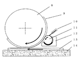
有機発光層の形成に用いる印刷機は、平板に印刷する方式のフレキソ印刷機であれば使用可能であるが、以下に示すような印刷機が望ましく、本発明の目的を達成するためには、印刷版へインキ供給手段については以下の構成になっていることが必須である。図2に印刷機の概略図を示した。本印刷機のインキ供給手段は、アニロックスロール11と、アニロックスロールの一部が常にインキに浸された状態になるよう構成されたインキ溜め部分(以下インキチャンバー12とする)とからなり、当該インキ供給手段は、印刷版9が取り付けされている版胴8にアニロックスロール11が接するように設置され、版胴8の回転に合わせてアニロックスロール11も回転しながら印刷版9にインキが供給される。また、版胴8が印刷時に1回転する内に、印刷版9へのインキ供給とステージ14上の基板13へのインキ転移が行われるように構成されている。インキタンクには、有機発光材料インキが収容されており、インキチャンバー12にはインキタンクより有機発光材料インキが送り込まれるようになっている。アニロックスロール11は、インキチャンバー12に溜められたインキにその一部が常に浸された状態で回転するようになっており、すなわちアニロックスロール11には常にインキが供給されるように構成されている。また、このアニロックスロール11は、印刷時には版胴8に接して回転することで、版へのインキ供給を可能となるように構成されている。
The printing machine used for forming the organic light emitting layer can be used as long as it is a flexographic printing machine that prints on a flat plate, but a printing machine as shown below is desirable, and in order to achieve the object of the present invention, It is essential that the ink supply means for the printing plate has the following configuration. FIG. 2 shows a schematic diagram of the printing press. The ink supply means of this printing machine includes an anilox roll 11 and an ink reservoir portion (hereinafter referred to as an ink chamber 12) configured so that a part of the anilox roll is always immersed in ink. The supply means is installed so that the anilox roll 11 is in contact with the
上記のように構成されたインキ供給手段におけるインキの転移過程を説明すると、表面に有機発光材料インキを保持するための微細なセル構造を有するアニロックスロール11を、その一部がインキに浸された状態で回転させながらドクターブレード10で余分なインキを掻き取ることで、アニロックスロール11表面にインキが均一に供給される。次に、アニロックスロール11は版胴8に接した状態で回転するため、印刷時に版胴8の回転によりアニロックスロール11と印刷版9が接して、アニロックスロール11から印刷版9の表面にインキが転移される。印刷版9の表面に転移されたインキは、アニロックスロール11から転移を受けたのと同一周回の内に被印刷基板13に接して基板上に転移される。
Explaining the ink transfer process in the ink supply means configured as described above, a part of the anilox roll 11 having a fine cell structure for holding the organic light emitting material ink on the surface is immersed in the ink. The ink is uniformly supplied to the surface of the anilox roll 11 by scraping off excess ink with the
本発明では、印刷版9がアニロックスロール11から有機発光材料インキの供給を受けてから基板13へインキを転移するまでの時間が5秒以下である必要がある。該時間を5秒以下に設定することにより、転移途中でのインキの乾きが抑制され、印刷に不具合が生じない。
本発明のさらに好ましい形態では、有機発光材料インキがアニロックスロール11に供給された時点から基板13へ該インキを転移するまでの時間が5秒以下である。なお、ここでいう「有機発光材料インキがアニロックスロール11に供給された時点」とは、アニロックスロールが浸漬インキ面を離れた時点を意味する。最も好ましい形態では、有機発光材料インキがアニロックスロール11に供給された時点から基板13へ該インキを転移するまでの時間が2秒以下である。これらの好ましい形態を採用することにより、転移途中でのインキの乾きがさらに抑制される。
In the present invention, the time from when the
In a more preferred embodiment of the present invention, the time from when the organic light emitting material ink is supplied to the anilox roll 11 until the ink is transferred to the substrate 13 is 5 seconds or less. Here, “the time when the organic light emitting material ink is supplied to the anilox roll 11” means the time when the anilox roll leaves the immersion ink surface. In the most preferable mode, the time from when the organic light emitting material ink is supplied to the anilox roll 11 until the ink is transferred to the substrate 13 is 2 seconds or less. By adopting these preferable forms, drying of the ink during the transfer is further suppressed.
有機発光層3の形成後、陰極層2を画素電極のラインパターンと直交するラインパターンで形成する。陰極層の材料としては、有機発光層の発光特性に応じたものを使用でき、例えば、リチウム、マグネシウム、カルシウム、イッテルビウム、アルミニウム等の金属単体やこれらと金、銀などの安定な金属との合金などが挙げられる。また、インジウム、亜鉛、錫などの導電性酸化物を用いることもできる。陰極層の形成方法としては、マスクを用いた真空蒸着法による形成方法が挙げられる。
最後に得られた有機EL素子を、外部の酸素や水分から保護するために、ガラスキャップ1と接着剤を用いて密封封止し、有機ELディスプレイ用の素子パネルを得ることができる。
After the organic
In order to protect the finally obtained organic EL element from external oxygen and moisture, the element panel for an organic EL display can be obtained by sealing and sealing with the
以下、本発明を実施例によりさらに説明するが、本発明は下記例に制限されるものではない。 EXAMPLES Hereinafter, although an Example demonstrates this invention further, this invention is not restrict | limited to the following example.
実施例1
実施例1においては、トルエンを溶媒として、有機発光材料であるポリフェニレンビニレン誘導体を濃度1%になるようにを溶解させた有機発光材料インキを用いて、凸版印刷法で発光層の形成を行った。また、使用した印刷機のインキ供給手段は、前記形態に示したように、アニロックスロールと、アニロックスロールの一部が常にインキに浸された状態になるよう構成されたインキチャンバーとからなり、当該インキ供給手段は、版胴に取り付けられている印刷版にアニロックスロールが接するように設置され、版胴の回転に合わせてアニロックスロールも回転しながら印刷版にインキが供給される。また、版胴が印刷時に1回転する内に、印刷版へのインキ供給と基板へのインキ転移が行われるように構成されていることで、アニロックスロールにインキが供給されてから、印刷版を介して最終的に基板に転写されるまでの時間を非常に短くすることが可能であり実際に印刷した条件では実測で1秒と2秒の間、計算上1.8秒であった。インキの溶媒として使用したトルエンの蒸気圧は20℃下で約2900Pa、25℃下で約3800Paである。
この発光層印刷は、画素電極の上にそのラインパターンにあわせて発光層のラインパターンが形成されるように行ったが、このとき使用した凸版印刷版は、芳香族有機溶媒に対しても耐性の高い水現像タイプの感光性樹脂版からなる凸版を用い、アニロックスロールは150線/インチのアニロックスロールおよび水現像タイプの感光性樹脂版を使用した。
Example 1
In Example 1, a light emitting layer was formed by a relief printing method using an organic light emitting material ink in which a polyphenylene vinylene derivative, which is an organic light emitting material, was dissolved at a concentration of 1% using toluene as a solvent. . Further, the ink supply means of the used printing press comprises an anilox roll and an ink chamber configured so that a part of the anilox roll is always immersed in the ink, as shown in the above embodiment, The ink supply means is installed so that the anilox roll contacts the printing plate attached to the plate cylinder, and the ink is supplied to the printing plate while the anilox roll rotates in accordance with the rotation of the plate cylinder. In addition, ink is supplied to the printing plate and transferred to the substrate while the plate cylinder rotates once during printing, so that the ink is supplied to the anilox roll. Thus, the time until the image is finally transferred to the substrate can be made very short. Under actual printing conditions, the actual measurement was between 1 and 2 seconds, and the calculation was 1.8 seconds. The vapor pressure of toluene used as an ink solvent is about 2900 Pa at 20 ° C. and about 3800 Pa at 25 ° C.
This light-emitting layer printing was performed so that the line pattern of the light-emitting layer was formed on the pixel electrode in accordance with the line pattern, but the relief printing plate used at this time was also resistant to aromatic organic solvents. The anilox roll used was a 150-line / inch anilox roll and a water-developable photosensitive resin plate.
その他、本実施例における有機ELディスプレイ用素子パネルの試作方法の詳細を以下に示す。
300mm角のガラス基板の上に、スパッタ法を用いてITO(インジウム−錫酸化物)薄膜を形成し、フォトリソ法と酸溶液によるエッチングでITO膜をパターニングして、対角5インチサイズのディスプレイが2面取れるように画素電極を形成した。ディスプレイ1面当たりの画素電極のラインパターンは、線幅80μm、スペース40μmでラインが840ライン形成されるパターンとした。
その上にスリットコート法で正孔輸送層を形成したが、正孔輸送材料インキとしてはPEDOT/PSSの水分散液からなるから成るインキを用いた。正孔輸送層の乾燥後の膜厚は50nmとした。
その上の発光層は、前記した方法で形成した。印刷、乾燥後の有機発光層の膜厚は80nmとなった。
その上にCa、Alからなる陰極層を画素電極のラインパターンと直交するようなラインパターンで抵抗過熱蒸着法によりマスク蒸着して形成した。最後にこれらの有機EL構成体を、外部の酸素や水分から保護するために、ガラスキャップと接着剤を用いて密閉封止し、有機ELディスプレイ用素子パネルを作成した。
また、発光層印刷後に別途サンプリングしておいたサンプルで、発光層中の溶媒の残留を評価した。
In addition, the detail of the trial production method of the element panel for organic EL displays in a present Example is shown below.
An ITO (indium-tin oxide) thin film is formed on a 300 mm square glass substrate by sputtering, and the ITO film is patterned by photolithography and etching with an acid solution. Pixel electrodes were formed so that two surfaces could be taken. The line pattern of the pixel electrode per display surface was a pattern in which 840 lines were formed with a line width of 80 μm and a space of 40 μm.
A hole transport layer was formed thereon by a slit coating method. As the hole transport material ink, an ink composed of an aqueous dispersion of PEDOT / PSS was used. The thickness of the hole transport layer after drying was 50 nm.
The light emitting layer thereon was formed by the method described above. The thickness of the organic light emitting layer after printing and drying was 80 nm.
A cathode layer made of Ca and Al was formed thereon by mask vapor deposition with a resistance overheating vapor deposition method in a line pattern orthogonal to the pixel electrode line pattern. Finally, in order to protect these organic EL constituents from external oxygen and moisture, they were hermetically sealed using a glass cap and an adhesive to produce an element panel for an organic EL display.
Moreover, the residual of the solvent in a light emitting layer was evaluated with the sample sampled separately after light emitting layer printing.
実施例2
実施例2においては、有機発光材料インキに使用する溶媒をo−キシレンとした他は、実施例1と全く同様にして有機ELディスプレイ用素子パネルを作成した。
o−キシレンの蒸気圧は、20℃下で約650Pa、25℃下では約830Paである。
Example 2
In Example 2, an element panel for an organic EL display was prepared in exactly the same manner as in Example 1, except that o-xylene was used as the solvent for the organic light emitting material ink.
The vapor pressure of o-xylene is about 650 Pa at 20 ° C. and about 830 Pa at 25 ° C.
実施例3
実施例3においては、有機発光材料インキに使用する溶媒を実施例2と同じo−キシレンとし、またアニロックスロールにインキが供給されてから、印刷版を介して最終的に基板に転写されるまでの時間を5秒とした他は、実施例1と全く同様にして有機ELディスプレイ用素子パネルを作成した。
Example 3
In Example 3, the solvent used in the organic light-emitting material ink is the same o-xylene as in Example 2, and after the ink is supplied to the anilox roll, it is finally transferred to the substrate through the printing plate. An element panel for an organic EL display was prepared in the same manner as in Example 1 except that the time of 5 was set to 5 seconds.
比較例1
比較例1においては、有機発光材料インキに使用する溶媒をアニソールとした他は、実施例1と全く同様にして有機ELディスプレイ用素子パネルを作成した。
アニソールの蒸気圧は、20℃下で約330Pa、25℃下では約470Paである。
Comparative Example 1
In Comparative Example 1, an element panel for organic EL display was prepared in exactly the same manner as in Example 1 except that the solvent used in the organic light emitting material ink was anisole.
The vapor pressure of anisole is about 330 Pa at 20 ° C. and about 470 Pa at 25 ° C.
比較例2
比較例2においては、有機発光材料インキに使用する溶媒をアニリンとした他は、実施例1と全く同様にして有機ELディスプレイ用素子パネルを作成した。
アニリンの蒸気圧は、20℃下で約57Pa、25℃下では約85Paである。
Comparative Example 2
In Comparative Example 2, an element panel for an organic EL display was prepared in exactly the same manner as in Example 1 except that aniline was used as the solvent for the organic light emitting material ink.
The vapor pressure of aniline is about 57 Pa at 20 ° C. and about 85 Pa at 25 ° C.
比較例3
比較例3においては、有機発光材料インキに使用する溶媒を実施例2と同じo−キシレンとし、またアニロックスロールにインキが供給されてから、印刷版を介して最終的に基板に転写されるまでの時間を8秒(内印刷版がインキの供給を受けてから基板に転移するまでの時間は6秒)とした他は、実施例1と全く同様にして有機ELディスプレイ用素子パネルを作成した。
o−キシレンの蒸気圧は、20℃下で約650Pa、25℃下では約830Paである。
Comparative Example 3
In Comparative Example 3, the solvent used for the organic light-emitting material ink is the same o-xylene as in Example 2, and after the ink is supplied to the anilox roll, it is finally transferred to the substrate through the printing plate. The element panel for an organic EL display was prepared in exactly the same manner as in Example 1 except that the period of time was set to 8 seconds (the time from the time when the inner printing plate was supplied with ink until it was transferred to the substrate was 6 seconds). .
The vapor pressure of o-xylene is about 650 Pa at 20 ° C. and about 830 Pa at 25 ° C.
[表1]

印刷性(印刷位置精度) ◎:非常に良好 ○:良好 ×:不良
残留溶媒 ○:検出されず △:わずかに検出 ×:検出
Printability (printing position accuracy) ◎: Very good ○: Good ×: Poor Residual solvent ○: Not detected △: Slightly detected ×: Detected
表1の結果から、トルエン、キシレンを溶媒とするインキを使用した実施例1〜3及び比較例3では、印刷・乾燥後の発光層から残留溶媒が検出されなかったのに対して、アニソール、アニリンを溶媒とするインキを使用した比較例1、2では残留溶媒が検出された。
また、インキ転移時間を2〜5秒とした実施例1〜3及び比較例1、2では印刷性良好であったのに対して、インキ転移時間8秒の比較例3では、印刷途中でのインキの乾燥によるインキ転移不良がみられた。インキ転移時間2〜5秒の中では、2秒の方がさらに良好であった。
これらの結果から、実施例1〜3のように、トルエンやキシレンといった蒸気圧が500Pa以上の乾燥しやすい溶媒のインキを用い、インキ転移時間を5秒以下にして印刷を行うことで、発光層への溶媒の残留がほとんど無く、しかも転移不良のない良好な印刷ができることが確認された。
From the results of Table 1, in Examples 1 to 3 and Comparative Example 3 using inks containing toluene and xylene as solvents, no residual solvent was detected from the light emitting layer after printing and drying, whereas anisole, In Comparative Examples 1 and 2 using an ink containing aniline as a solvent, residual solvent was detected.
In addition, in Examples 1 to 3 and Comparative Examples 1 and 2 in which the ink transfer time was 2 to 5 seconds, the printability was good, whereas in Comparative Example 3 with an ink transfer time of 8 seconds, Ink transfer failure due to ink drying was observed. Of the ink transfer times of 2-5 seconds, 2 seconds was even better.
From these results, as in Examples 1 to 3, by using ink of a solvent that is easily dried such as toluene and xylene with a vapor pressure of 500 Pa or more, and performing printing with an ink transfer time of 5 seconds or less, the light emitting layer It was confirmed that there was almost no solvent remaining in the film, and good printing without transfer failure was possible.
本発明の製造方法では、有機発光材料に対する溶解性の高いトルエンやキシレンといった一般的な室温環境での蒸気圧が500Paより大きい芳香族有機溶媒を用いても、乾燥による印刷の不具合が生じない印刷手段が提供され、凸版印刷法による発光層のより良好な形成を可能とし、有機EL素子の製造方法として有用である。 In the production method of the present invention, even when an aromatic organic solvent having a vapor pressure of more than 500 Pa in a general room temperature environment such as toluene or xylene having high solubility in an organic light-emitting material is used, printing problems do not occur due to drying. Means are provided to enable better formation of the light-emitting layer by letterpress printing and are useful as a method for producing an organic EL device.
1……ガラスキャップ、2……陰極、3……発光層、4……正孔輸送層、5……画素電極、6……ガラス基板、7……絶縁層、8……版胴、9……印刷版、10……ドクターブレード、11……アニロックスロール、12……インキチャンバー、13……基板、14……ステージ。
DESCRIPTION OF
Claims (2)
前記有機発光材料インキの溶媒が、20〜25℃での蒸気圧が500Paより大きい溶媒からなり、かつ前記印刷版が前記有機発光材料インキの供給を受けてから前記基板へ該インキを転移するまでの時間が5秒以下であり、
前記印刷版へのインキ供給手段が、アニロックスロールと、前記アニロックスロールの一部が常に前記有機発光材料インキに浸された状態になるよう構成されたインキチャンバーとからなり、
前記インキチャンバーは、インキタンクから前記有機発光材料インキが送り込まれて前記有機発光材料インキを溜めており、
版胴に取り付けられている前記印刷版に前記アニロックスロールが接するように設置され、前記版胴の回転に合わせて前記アニロックスロールも回転しながら前記印刷版に該インキが供給され、版胴が印刷時に1回転する内に、前記印刷版へのインキ供給と前記基板へのインキ転移が行われるように構成されている
ことを特徴とする有機エレクトロルミネッセンス素子の製造方法。 An organic electroluminescent element manufacturing method for forming an organic light emitting layer by using a relief printing method in which organic luminescent material ink is printed while sequentially transferring from an ink supply means to a printing plate to a printing plate and from the printing plate to a substrate. There,
The solvent of the organic light emitting material ink is a solvent having a vapor pressure at 20 to 25 ° C. higher than 500 Pa, and the printing plate receives the supply of the organic light emitting material ink and transfers the ink to the substrate time is 5 seconds der following is,
The ink supply means to the printing plate comprises an anilox roll, and an ink chamber configured so that a part of the anilox roll is always immersed in the organic light emitting material ink,
The ink chamber is fed with the organic light emitting material ink from an ink tank and stores the organic light emitting material ink,
The anilox roll is installed in contact with the printing plate attached to the plate cylinder, and the ink is supplied to the printing plate while the anilox roll is rotated in accordance with the rotation of the plate cylinder, and the plate cylinder is printed. The method of manufacturing an organic electroluminescence element, wherein the ink supply to the printing plate and the ink transfer to the substrate are performed within one rotation .
Priority Applications (2)
| Application Number | Priority Date | Filing Date | Title |
|---|---|---|---|
| JP2007160176A JP4935525B2 (en) | 2007-06-18 | 2007-06-18 | Method for manufacturing organic electroluminescence device |
| US12/140,222 US8231933B2 (en) | 2007-06-18 | 2008-06-16 | Method for manufacturing organic electroluminescence device |
Applications Claiming Priority (1)
| Application Number | Priority Date | Filing Date | Title |
|---|---|---|---|
| JP2007160176A JP4935525B2 (en) | 2007-06-18 | 2007-06-18 | Method for manufacturing organic electroluminescence device |
Publications (2)
| Publication Number | Publication Date |
|---|---|
| JP2008311182A JP2008311182A (en) | 2008-12-25 |
| JP4935525B2 true JP4935525B2 (en) | 2012-05-23 |
Family
ID=40132590
Family Applications (1)
| Application Number | Title | Priority Date | Filing Date |
|---|---|---|---|
| JP2007160176A Expired - Fee Related JP4935525B2 (en) | 2007-06-18 | 2007-06-18 | Method for manufacturing organic electroluminescence device |
Country Status (2)
| Country | Link |
|---|---|
| US (1) | US8231933B2 (en) |
| JP (1) | JP4935525B2 (en) |
Families Citing this family (2)
| Publication number | Priority date | Publication date | Assignee | Title |
|---|---|---|---|---|
| JP2013157277A (en) * | 2012-01-31 | 2013-08-15 | Canon Inc | Light-emitting device, image formation device, and imaging device |
| CN115851032B (en) * | 2022-12-23 | 2023-12-22 | 北京印刷学院 | Electroluminescent flexographic printing ink and preparation method thereof |
Family Cites Families (11)
| Publication number | Priority date | Publication date | Assignee | Title |
|---|---|---|---|---|
| JP3025166B2 (en) * | 1995-02-10 | 2000-03-27 | 三菱重工業株式会社 | Ink supply control unit for flexographic printing press |
| JPH11227151A (en) * | 1998-02-13 | 1999-08-24 | Asahi Glass Co Ltd | Flexographic press |
| JP2001093668A (en) | 1999-09-22 | 2001-04-06 | Canon Inc | Organic light-emitting material, display material using the same and method for manufacturing |
| JP2001155858A (en) | 1999-11-24 | 2001-06-08 | Sharp Corp | Method of manufacturing organic el element |
| JP3836282B2 (en) | 1999-11-24 | 2006-10-25 | シャープ株式会社 | Organic EL coating liquid, organic EL element and method for producing the same. |
| US6582504B1 (en) | 1999-11-24 | 2003-06-24 | Sharp Kabushiki Kaisha | Coating liquid for forming organic EL element |
| JP2006252787A (en) * | 2005-03-08 | 2006-09-21 | Toppan Printing Co Ltd | Manufacturing method of organic el element and organic el element |
| US7485023B2 (en) * | 2005-03-31 | 2009-02-03 | Toppan Printing Co., Ltd. | Organic electroluminescent device having partition wall and a manufacturing method of the same by relief printing method |
| JP2006286241A (en) * | 2005-03-31 | 2006-10-19 | Toppan Printing Co Ltd | Organic el display panel and its manufacturing method |
| JP4793688B2 (en) * | 2006-04-26 | 2011-10-12 | 凸版印刷株式会社 | Organic EL printing machine and organic EL device manufacturing method |
| US7546803B2 (en) * | 2006-01-30 | 2009-06-16 | Toppan Printing Co., Ltd. | Letterpress printing machine |
-
2007
- 2007-06-18 JP JP2007160176A patent/JP4935525B2/en not_active Expired - Fee Related
-
2008
- 2008-06-16 US US12/140,222 patent/US8231933B2/en active Active
Also Published As
| Publication number | Publication date |
|---|---|
| US20080311284A1 (en) | 2008-12-18 |
| JP2008311182A (en) | 2008-12-25 |
| US8231933B2 (en) | 2012-07-31 |
Similar Documents
| Publication | Publication Date | Title |
|---|---|---|
| JP2008140724A (en) | Organic el element and manufacturing method of same | |
| JP4826119B2 (en) | Manufacturing method of organic EL element | |
| JP4706845B2 (en) | Manufacturing method of organic EL element | |
| JP5315586B2 (en) | Manufacturing method of electronic device using relief printing plate for high definition and organic EL element | |
| JP4935525B2 (en) | Method for manufacturing organic electroluminescence device | |
| JP2006252787A (en) | Manufacturing method of organic el element and organic el element | |
| JP2008134513A (en) | Resin letterpress and method for manufacturing element panel for organic el display | |
| JP2009059496A (en) | Organic el printer | |
| JP4626817B2 (en) | Letterpress for letterpress printing and printed matter | |
| JP4747637B2 (en) | Manufacturing method of organic EL display panel | |
| JP2010083130A (en) | Letterpress printer | |
| JP4645311B2 (en) | Organic EL element manufacturing method and organic EL element manufacturing apparatus | |
| JP2011113654A (en) | Organic el element and method of manufacturing the same | |
| JP4826189B2 (en) | Electroluminescent element manufacturing method and electroluminescent element | |
| JP2014067543A (en) | Organic el element and method for manufacturing organic el element | |
| JP2009081107A (en) | Method for manufacturing organic electroluminescent element | |
| JP2008135326A (en) | Manufacturing method of high definition display | |
| JP6295509B2 (en) | Topographic printing device | |
| JP6127571B2 (en) | Letterpress printing apparatus and organic EL element manufacturing method | |
| JP6035807B2 (en) | Topographic printing device | |
| JP5391559B2 (en) | Printing machine and method for producing printed matter using the same | |
| JP2014065222A (en) | Printer for manufacturing organic el panel and method for manufacturing organic el panel | |
| JP2007168151A (en) | Manufacturing method of letterpress for printing and printed matter | |
| JP2010228202A (en) | Letterpress printing apparatus, method for forming pattern, method for manufacturing electronic device, method for manufacturing organic electroluminescent element | |
| JP2014157764A (en) | Precision printing method and precision printed product |
Legal Events
| Date | Code | Title | Description |
|---|---|---|---|
| A621 | Written request for application examination |
Free format text: JAPANESE INTERMEDIATE CODE: A621 Effective date: 20100524 |
|
| A521 | Request for written amendment filed |
Free format text: JAPANESE INTERMEDIATE CODE: A523 Effective date: 20110524 |
|
| A977 | Report on retrieval |
Free format text: JAPANESE INTERMEDIATE CODE: A971007 Effective date: 20111026 |
|
| A131 | Notification of reasons for refusal |
Free format text: JAPANESE INTERMEDIATE CODE: A131 Effective date: 20111111 |
|
| A521 | Request for written amendment filed |
Free format text: JAPANESE INTERMEDIATE CODE: A523 Effective date: 20120106 |
|
| TRDD | Decision of grant or rejection written | ||
| A01 | Written decision to grant a patent or to grant a registration (utility model) |
Free format text: JAPANESE INTERMEDIATE CODE: A01 Effective date: 20120124 |
|
| A01 | Written decision to grant a patent or to grant a registration (utility model) |
Free format text: JAPANESE INTERMEDIATE CODE: A01 |
|
| A61 | First payment of annual fees (during grant procedure) |
Free format text: JAPANESE INTERMEDIATE CODE: A61 Effective date: 20120206 |
|
| FPAY | Renewal fee payment (event date is renewal date of database) |
Free format text: PAYMENT UNTIL: 20150302 Year of fee payment: 3 |
|
| R150 | Certificate of patent or registration of utility model |
Ref document number: 4935525 Country of ref document: JP Free format text: JAPANESE INTERMEDIATE CODE: R150 Free format text: JAPANESE INTERMEDIATE CODE: R150 |
|
| LAPS | Cancellation because of no payment of annual fees |