JP4931329B2 - Capacitor, wiring board, decoupling circuit and high frequency circuit - Google Patents
Capacitor, wiring board, decoupling circuit and high frequency circuit Download PDFInfo
- Publication number
- JP4931329B2 JP4931329B2 JP2003335812A JP2003335812A JP4931329B2 JP 4931329 B2 JP4931329 B2 JP 4931329B2 JP 2003335812 A JP2003335812 A JP 2003335812A JP 2003335812 A JP2003335812 A JP 2003335812A JP 4931329 B2 JP4931329 B2 JP 4931329B2
- Authority
- JP
- Japan
- Prior art keywords
- conductor
- capacitor
- layer
- conductors
- conductor layer
- Prior art date
- Legal status (The legal status is an assumption and is not a legal conclusion. Google has not performed a legal analysis and makes no representation as to the accuracy of the status listed.)
- Expired - Fee Related
Links
Images


Description
本発明は、コンデンサ、配線基板、デカップリング回路及び高周波回路に関するもので、特に、高周波領域において有利に適用され得るコンデンサ、ならびに、このコンデンサを用いて構成される、配線基板、デカップリング回路及び高周波回路に関するものである。 The present invention relates to a capacitor, a wiring board, a decoupling circuit, and a high-frequency circuit, and in particular, a capacitor that can be advantageously applied in a high-frequency region, and a wiring board, a decoupling circuit, and a high-frequency wave that are configured using this capacitor. It relates to the circuit.
代表的なコンデンサとして、積層コンデンサを例にとって説明する。 As a typical capacitor, a multilayer capacitor will be described as an example.
積層コンデンサを用いた等価回路では、コンデンサの静電容量をC、等価直列インダクタンス(ESL)をLとしたとき、共振周波数(f0)は、f0=1/〔2π×(L×C)1/2〕の関係で表され、共振周波数(f0)より高い周波数領域では、コンデンサの機能が消失してしまうことが知られている。すなわち、一定値以上の静電容量(C)を維持するためには、できるだけESL(L)を低くする必要がある。つまり、ESLが低ければ、共振周波数(f0)は高くなり、より高周波領域で使用できることになる。このことから、積層コンデンサをマイクロ波領域で使うためには、より低ESL化が図られたものが必要となる。 In an equivalent circuit using a multilayer capacitor, when the capacitance of the capacitor is C and the equivalent series inductance (ESL) is L, the resonance frequency (f 0 ) is f 0 = 1 / [2π × (L × C). expressed in relation 1/2], in the frequency region higher than the resonance frequency (f 0), it is known that the function of the capacitor is lost. That is, in order to maintain an electrostatic capacity (C) of a certain value or more, it is necessary to make ESL (L) as low as possible. That is, if the ESL is low, the resonance frequency (f 0 ) is high and can be used in a higher frequency region. For this reason, in order to use the multilayer capacitor in the microwave region, it is necessary to further reduce the ESL.
また、ワークステーションやパーソナルコンピュータ等のマイクロプロセッシングユニット(MPU)のMPUチップに電源を供給するために用いられ、通常デカップリングコンデンサとして配線基板上に接続されている積層コンデンサも、
近年のMPUの高速、高周波化に伴って、低ESL化が求められている。
In addition, a multilayer capacitor that is used to supply power to an MPU chip of a microprocessing unit (MPU) such as a workstation or a personal computer, and is usually connected as a decoupling capacitor on a wiring board,
With the recent increase in speed and frequency of MPUs, there is a demand for lower ESL.
ここで、従来の積層コンデンサについて、図6(a)、(b)をもとに説明する。(a)は第1及び第2導体層の重なり状態を示す概略図、(b)は(a)のX−X線断面図である。 Here, a conventional multilayer capacitor will be described with reference to FIGS. 6 (a) and 6 (b). (A) is the schematic which shows the overlapping state of the 1st and 2nd conductor layer, (b) is XX sectional drawing of (a).
図に示す従来の積層コンデンサ50は、誘電体層52の一方主面に第1導体層53が、他方主面に第2導体層54が夫々形成され、これらの誘電体層52が複数積層されており、また、これらの誘電体層52の厚み方向には第1及び第2導体層53、54同士を夫々接続する第1及び第2貫通導体55、56が形成され、
積層体51が構成されている。そして、ここでは、第1及び第2貫通導体55、56が、積層体51の一方の最表面に露出し、夫々第1及び第2接続端子57、58に接続され、積層コンデンサ50が構成されている。さらに、第1及び第2導体層53、54内に、第2及び第1貫通導体56、55とは夫々接続しない第1及び第2非導体形成領域63、64が形成されている。
In the
A laminated
そして、第1及び第2貫通導体55、56は、第1及び第2導体層53、54の全域にわたって、交互に格子状に分散して配置されている。
The first and second through
上記積層コンデンサ50によれば、静電容量は、第1及び第2導体層53、54の内、主に第1及び第2貫通導体55、56に囲まれた部分に発生していた。
According to the
また、上記積層コンデンサ50の製造方法は、未焼成状態の積層体1に、脱バインダ処理、焼成を行い、積層体1を得た後、第1及び第2接続端子7、8を形成していた(特許文献1乃至4参照)。
しかしながら、上記積層コンデンサ50によれば、低ESL化を図るためには、第1及び第2貫通導体55、56の数を増加するとともに、これらの中心間の距離を小さくする方法が考えられるが、第1及び第2貫通導体55、56の数を増加した場合、第1及び第2導体層53、54内の非導体形成領域63、64の面積が増大するため、積層コンデンサ50の静電容量が低下するという問題点があった。一方、上記中心間の距離を小さくした場合、未焼成状態の積層体1のハンドリングや、焼成時の誘電体層2と第1及び第2貫通導体55、56の収縮率の差、ICパッケージなどへの実装時の誘電体層2と第1及び第2貫通導体55、56との熱膨張係数の差などにより、第1及び第2貫通導体55、56にまたがるように、クラックが発生するという問題点があった。
However, according to the
また、上記積層コンデンサ50によれば、第1導体層53と第2非導体形成領域64、あるいは第2導体層54と第1非導体形成領域63が重なる部分は、静電容量が発生しないため、積層コンデンサ50の高容量化には限界があった。
Further, according to the
本発明は、上述の問題点に鑑みて案出されたものであり、その目的は、低ESL且つ高容量を実現し、且つクラックの発生を抑制できるコンデンサを提供することである。 The present invention has been devised in view of the above-described problems, and an object of the present invention is to provide a capacitor capable of realizing low ESL and high capacity and suppressing the occurrence of cracks.
本発明の他の目的は、上述したようなコンデンサを用いて構成される、配線基板、デカップリング回路及び高周波回路を提供することである。 Another object of the present invention is to provide a wiring board, a decoupling circuit, and a high-frequency circuit that are configured using a capacitor as described above.
本発明のコンデンサは、誘電体層の一方主面に第1導体層が、前記誘電体層の他方主面に第2導体層が配設されるとともに、前記誘電体層の厚み方向に、前記第2導体層と第1非導体形成領域によって隔てられ、且つ前記第1導体層に接続される複数の第1貫通導体と、前記第1導体層と第2非導体形成領域によって隔てられ、且つ前記第2導体層に接続される複数の第2貫通導体とが形成されてなるコンデンサにおいて、
2つの前記第1貫通導体及び2つの前記第2貫通導体が格子状に配置されて格子の縦横の方向に隣接する前記第1貫通導体の前記第1非導体形成領域と前記第2貫通導体の前記第2非導体形成領域とが積層方向に重なり合った貫通導体群を複数形成しているとともに、複数の前記貫通導体群が互いに一様な距離をもって配置され、前記第1導体層及び前記第2導体層の周縁部と前記貫通導体群との間に、前記格子の縦横の方向に隣接する前記第1貫通導体と前記第2貫通導体との中心間の間隔以上の幅で、前記第1導体層及び前記第2導体層が存在していることを特徴とするものである。
In the capacitor of the present invention, the first conductor layer is disposed on one main surface of the dielectric layer, the second conductor layer is disposed on the other main surface of the dielectric layer, and the thickness direction of the dielectric layer A plurality of first through conductors separated by a second conductor layer and a first non-conductor formation region and connected to the first conductor layer; and separated by the first conductor layer and a second non-conductor formation region; and In a capacitor formed with a plurality of second through conductors connected to the second conductor layer,
The two first through conductors and the two second through conductors are arranged in a lattice shape, and the first non-conductor forming region of the first through conductor and the second through conductor adjacent to each other in the vertical and horizontal directions of the lattice. A plurality of through conductor groups in which the second non-conductor forming region overlaps in the stacking direction are formed, and the plurality of through conductor groups are arranged at a uniform distance from each other, and the first conductor layer and the second conductor group between the through conductor group and the peripheral portion of the conductor layer, at intervals over the width between the centers of said first through conductor and the second through-conductor adjacent to the longitudinal and lateral directions of the grating, the first conductor A layer and the second conductor layer are present.
また、前記貫通導体群が、前記第1及び第2貫通導体及び前記第1及び第2導体層を流れる電流によって誘起される磁界を互いに相殺するように配置される。 Further, the through conductor group is disposed so as to cancel out magnetic fields induced by currents flowing through the first and second through conductors and the first and second conductor layers.
また、前記貫通導体群内において、前記第1及び第2の貫通導体が、実質的に正方形の各頂点に位置する分布状態をもって互いに隣り合うように配置される。 Further, in the through conductor group, the first and second through conductors are arranged so as to be adjacent to each other with a distribution state positioned substantially at each vertex of the square.
また、本発明は上述のコンデンサを備えた配線基板にも適用できる。 The present invention can also be applied to a wiring board provided with the above-described capacitor.
さらに、本発明に係るコンデンサは、MPUに備えるMPUチップのための電源回路に接続されるデカップリングコンデンサとしても有利に用いられる。 Furthermore, the capacitor according to the present invention can be advantageously used as a decoupling capacitor connected to a power supply circuit for an MPU chip included in the MPU.
また、本発明は、上述のコンデンサを備えた高周波回路にも適用できる。 The present invention can also be applied to a high-frequency circuit including the above-described capacitor.
以上の通り、本発明のコンデンサによれば、2つの第1貫通導体及び2つの第2貫通導体が格子状に配置されて格子の縦横の方向に隣接する第1貫通導体の第1非導体形成領域と第2貫通導体の第2非導体形成領域とが積層方向に重なり合った貫通導体群の複数が、互いに一様な距離をもって配置されているため、貫通導体群内のみに流れる電流は、流れる距離が短くなることから、電流によって誘起される磁束に起因する自己インダクタンス成分が低くなる。このため、コンデンサ全体の等価直列インダクタンス(ESL)を低くできる。また、ESLを低くするために、第1及び第2貫通導体の数を増加する必要がないため、コンデンサの高容量化を実現できる。さらに、貫通導体群間に、貫通導体の無い領域が存在するため、複数の貫通導体群にまたがるように応力が発生することを防止でき、コンデンサのクラックの発生を抑制できる。 As described above, according to the capacitor of the present invention, two first through-conductors and two second first non of the first through conductor penetrating conductors are adjacent are arranged in a grid pattern in the direction of the vertical and horizontal grid Since a plurality of through conductor groups in which the conductor forming region and the second non-conductor forming region of the second through conductor overlap in the stacking direction are arranged at a uniform distance from each other , the current flowing only in the through conductor group is Since the flowing distance is shortened, the self-inductance component caused by the magnetic flux induced by the current is lowered. For this reason, the equivalent series inductance (ESL) of the whole capacitor can be reduced. Further, since it is not necessary to increase the number of first and second through conductors in order to reduce the ESL, it is possible to realize a high capacity capacitor. Furthermore, since there is a region without through conductors between the through conductor groups, it is possible to prevent stress from being generated across a plurality of through conductor groups and to suppress the occurrence of cracks in the capacitor.
また、貫通導体群を構成し、且つ隣接しあう第1貫通導体と第2貫通導体との間に容量の発生する領域が存在しないため、第1貫通導体から他方、例えば第2貫通導体へ流れる電流は、ほとんど無くなる。このことにより、電流によって誘起される磁束に起因する自己インダクタンス成分が極めて低くなり、コンデンサ全体のESLをさらに低くすることができる。また、第1導体層と第2非導体形成領域、あるいは第2導体層と第1非導体形成領域が重なる部分の面積が減少するため、コンデンサのさらなる高容量化を実現できる。 In addition, since there is no region where a capacitance is generated between the first through conductor and the second through conductor that constitute the through conductor group and are adjacent to each other, the first through conductor flows to the other, for example, the second through conductor. The current is almost gone. As a result, the self-inductance component due to the magnetic flux induced by the current becomes extremely low, and the ESL of the entire capacitor can be further reduced. In addition, since the area of the portion where the first conductor layer and the second non-conductor forming region or the portion where the second conductor layer and the first non-conductor forming region overlap is reduced, it is possible to further increase the capacity of the capacitor.
さらに、第1導体層及び第2導体層の周縁部と貫通導体群の間に、第1貫通導体と第2貫通導体との中心間の間隔P以上の幅で、第1貫通導体、第2貫通導体及び非導体形成領域の無い、静電容量領域が形成されているため、静電容量領域の第1導体層及び第2導体層に流れる電流の量が多くなり、このことによってもコンデンサ全体のESLをさらに効果的に低くすることができる。また、貫通導体群の周囲に静電容量が発生するため、加わる電界を大きくすることができ、このことによってもコンデンサの高容量化を実現できる。 Further, the first through conductor, the second through the first conductor layer and the second conductor layer with a width equal to or greater than the distance P between the centers of the first through conductor and the second through conductor between the peripheral portions of the first conductor layer and the second conductor layer and the through conductor group. Since the capacitance region without the through conductor and non-conductor formation region is formed, the amount of current flowing through the first conductor layer and the second conductor layer in the capacitance region increases, and this also causes the entire capacitor ESL can be further effectively reduced. Further, since electrostatic capacitance is generated around the through conductor group, the applied electric field can be increased, and this also makes it possible to increase the capacity of the capacitor.
またさらに、貫通導体群が、貫通導体及び導体層を流れる電流によって誘起される磁界を互いに相殺するように配置されるため、コンデンサ全体のESLをさらに効果的に低くすることができる。 Furthermore, since the through conductor group is disposed so as to cancel each other out of the magnetic field induced by the current flowing through the through conductor and the conductor layer, the ESL of the entire capacitor can be further effectively reduced.
さらにまた、貫通導体群が、一様な距離をもって互いに隣り合うように配置されるため、貫通導体群間で部分的にESLが高くなることがなく、コンデンサ全体のESLをさらに効果的に低くすることができる。 Furthermore, since the through conductor groups are arranged so as to be adjacent to each other with a uniform distance, the ESL is not partially increased between the through conductor groups, and the ESL of the entire capacitor is further effectively reduced. be able to.
そして、貫通導体群内において、第1及び第2の貫通導体が、実質的に正方形の各頂点に位置する分布状態をもって互いに隣り合うように配置されるため、貫通導体群内で部分的にESLが高くなることがなく、コンデンサ全体のESLをさらに効果的に低くすることができる。 In the through conductor group, the first and second through conductors are arranged so as to be adjacent to each other with a distribution state positioned substantially at each vertex of the square. The ESL of the entire capacitor can be further effectively reduced.
また、本発明は、上述のコンデンサを備えた配線基板、MPUに備えるMPUチップのための電源回路に接続されるデカップリングコンデンサとしても有利に用いられる。 The present invention is also advantageously used as a decoupling capacitor connected to a power supply circuit for an MPU chip provided in an MPU or a wiring board provided with the above-described capacitor.
また、本発明は、上述のコンデンサを備えた高周波回路にも適用できる。 The present invention can also be applied to a high-frequency circuit including the above-described capacitor.
以下、本発明のコンデンサ、配線基板、デカップリング回路及び高周波回路を図面に基づいて詳説する。 Hereinafter, a capacitor, a wiring board, a decoupling circuit, and a high frequency circuit of the present invention will be described in detail with reference to the drawings.
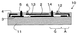
図1は本発明のコンデンサの一例である積層コンデンサを示す図であり、(a)は第1及び第2導体層の重なり状態を示す概略図、(b)は(a)のX−X線断面図である。 FIG. 1 is a view showing a multilayer capacitor as an example of the capacitor of the present invention, wherein (a) is a schematic view showing an overlapping state of first and second conductor layers, and (b) is an XX line of (a). It is sectional drawing.
図において、10は積層コンデンサ、2は誘電体層、3、4は第1及び第2導体層(内部電極層)、5、6は第1及び第2貫通導体(ビアホール導体)、7、8は第1及び第2接続端子である。 In the figure, 10 is a multilayer capacitor, 2 is a dielectric layer, 3 and 4 are first and second conductor layers (internal electrode layers), 5 and 6 are first and second through conductors (via hole conductors), and 7 and 8. Are first and second connection terminals.
図に示すように、積層コンデンサ10は、誘電体層2の一方主面に第1導体層3が、他方主面に第2導体層4が夫々形成され、これらの誘電体層2が複数積層されており、また、これらの誘電体層2の厚み方向には第1及び第2導体層3、4同士を夫々接続する複数の第1及び第2貫通導体5、6が形成され、積層体1が構成されている。そして、ここでは、複数の第1及び第2貫通導体5、6が、積層体1の一方の最表面に露出し、第1及び第2接続端子7、8に接続され、積層コンデンサ10が構成されている。さらに、第1及び第2導体層3、4内に、第2及び第1貫通導体6、5とは夫々接続しない第1及び第2非導体形成領域13、14が形成されている。
As shown in the figure, in the
そして、第1及び第2貫通導体5、6は、例えば2つの第1貫通導体5と2つの第2貫通導体6が互いに格子状となるようにして貫通導体群Gを構成し、この貫通導体群Gが第1導体層3及び第2導体層4に分散して配置されている。例えば、図1では、4つの貫通導体群Gで構成され、平面視、矩形状の各頂点となる位置に配置されている。
The first and second through
誘電体層2は、チタン酸バリウムを主成分とする非還元性誘電体材料、及びガラス成分を含む誘電体材料からなり、この誘電体層2が図上、上方向に積層して積層体1が構成される。なお、誘電体層2の形状、厚み、積層数は容量値によって任意に変更することができる。第1及び第2導体層3、4は、Ni、Cu、あるいはこれらの合金を主成分とする材料から構成され、その厚みは1〜2μmとしている。
The
第1及び第2接続端子7、8は、半田バンプ、半田ボールなどが用いられる。
For the first and
本発明の特徴的なことは、少なくとも一対の第1貫通導体5及び第2貫通導体6(図1では2対の第1貫通導体5及び第2貫通導体6)とが近接してなる貫通導体群Gが、一様な距離をもって配置されていることである。
The characteristic of the present invention is that at least a pair of first through
また、貫通導体群Gを構成し、且つ隣接しあう第1貫通導体5と第2貫通導体6との間に容量の発生する領域が存在しない。具体的には、近接してなる第1貫通導体5の中心と第2貫通導体6の中心との間隔をP、非導体形成領域13、14の半径をm1、m2としたときに、P≦m1+m2の関係を満足する。ここで、等価直列抵抗(ESR)の増大を防ぐためには、第1及び第2の貫通導体3、4の半径を夫々r1、r2としたときに、r1+m2≦P、あるいはr2+m1≦Pの関係を満足することが望ましい。また、高容量を実現するためには、P>1.4m1、且つP>1.4m2の関係にあることが望ましい。
Further, there is no region where a capacitance is generated between the first through
さらに、第1導体層3及び第2導体層4の周縁部と貫通導体群Gの間に、間隔P以上の幅dで、第1貫通導体5、第2貫通導体6及び非導体形成領域13、14の無い、静電容量領域Aが形成されている。好ましくはd≧1.5P、さらに好ましくはd≧2Pの関係にあることが望ましい。
Further, the first through
またさらに、貫通導体群Gが、貫通導体5、6及び導体層3、4を流れる電流によって誘起される磁界を互いに相殺するように配置されている。
Furthermore, the through conductor group G is disposed so as to cancel out magnetic fields induced by currents flowing through the through
さらにまた、貫通導体群Gが、一様な距離をもって互いに隣り合うように配置されている。 Furthermore, the through conductor groups G are arranged adjacent to each other with a uniform distance.
そして、貫通導体群G内において、第1及び第2の貫通導体5、6が、実質的に正方形の各頂点に位置する分布状態をもって互いに隣り合うように配置されている。
In the through conductor group G, the first and second through
次に、本発明の積層コンデンサ10の製造方法について説明する。なお、図面において、各符号は焼成の前後で区別しないことにする。
Next, a method for manufacturing the
まず、誘電体層となるセラミックグリーンシート2に、第1及び第2導体層となる導体膜3、4を導電性ペーストの印刷・乾燥により形成する。このとき、第1及び第2非導体形成領域13、14も形成される。なお、誘電体層2として、他のペロブスカイト構造を持つセラミック材料や、有機強誘電体材料を用いても良い。
First,
次に、導体膜3、4が形成されたグリーンシート2を交互に所要枚数を積み重ね、積層体1が抽出される大型積層体を形成する。
Next, the required number of
次に、レーザの照射や、マイクロドリル又はパンチングを用いた打ち抜き法などにより、大型積層体の主面に導体膜3、4、セラミックグリーンシート2を貫く貫通孔を形成する。
Next, through holes penetrating the
次に、この貫通孔に導体層3、4に用いる導電性ペーストと同様の導電性ペーストを充填することにより、第1及び第2貫通導体となる導体部5、6が形成される。
Next, the
なお、誘電体層となるセラミックグリーンシート2に、マイクロドリル又はパンチングを用いた打ち抜き法などにより、あらかじめ貫通孔をあけておき、スクリーン印刷法により、セラミックグリーンシート2上に導体層3、4となる導体膜を印刷すると同時に、貫通孔に導電性ペーストを充填することにより、導体部5、6を形成後、積層するようにしても良い。
In addition, through holes are made in advance in the ceramic
次に、大型積層体を押し切り刃加工、ダイシング方式などにより切断し、未焼成状態の積層体1を得る。
Next, the large-sized laminate is cut by a press cutting process, a dicing method, or the like to obtain the
次に、この未焼成状態の積層体1は、脱バインダ処理後、焼成を行い、内部に第1及び第2導体層3、4、第1及び第2貫通導体5、6が形成されるとともに、一方主面に第1及び第2貫通導体5、6が露出した積層体1が得られる。
Next, the
このとき、積層体1の一方主面に露出した第1及び第2貫通導体5、6は、表面が酸化されているため、表面研磨により、酸化被膜を除去する。
At this time, since the surfaces of the first and second through
次に、第1及び第2貫通導体5、6の露出部に、Niメッキ、Snメッキを形成する。
Next, Ni plating and Sn plating are formed on the exposed portions of the first and second through
次に、半田ペーストをスクリーン印刷する方法や、フラックスを塗布後半田ボールを搭載する方法により、第1及び第2接続端子7、8となる半田を形成した後、リフロー処理を施すことにより、第1及び第2接続端子7、8が形成される。
Next, by forming a solder to be the first and
このようにして、図1に示すような積層コンデンサ10が得られる。
Thus, the
特に、複数の第1貫通導体5及び第2貫通導体6が一カ所に集中することがないため、誘電体の強度が維持・向上し、焼成時において、第1貫通導体5、第2貫通導体6でのクラックの発生を未然に防止できる。
In particular, since the plurality of first through
なお、本発明は以上の実施形態に限定されるものではなく、本発明の要旨を逸脱しない範囲で種々の変更・改良を加えることは何ら差し支えない。 In addition, this invention is not limited to the above embodiment, A various change and improvement can be added in the range which does not deviate from the summary of this invention.
図2は、本発明の積層コンデンサ10の他の実施の形態の概略図である。図2では、貫通導体群Gは、一対の第1及び第2貫通導体5、6が近接するように並んで構成されている。しかも、貫通導体群Gを構成する第1及び第2貫通導体5、6の配列方向が、各貫通導体群Gで異なっているため、複数の貫通導体群Gにまたがるように応力が発生することによるコンデンサ全体のクラックを、より効果的に抑制できる。
FIG. 2 is a schematic view of another embodiment of the
図3は、本発明の積層コンデンサ10のさらに他の実施の形態を示す断面図である。図のように、第1及び第2貫通導体5、6が積層体1の両主面に露出しても良い。このことにより、ICパッケージとIC素子との間や、ICパッケージ内部に、本積層コンデンサ10を介在させて実装することができる。
FIG. 3 is a cross-sectional view showing still another embodiment of the
図4は、本発明の積層コンデンサ10のさらに他の実施の形態を示す断面図である。図のように、絶縁基板11の表面に、第1導体層3、誘電体層2、第2導体層4、保護層12が順次被着形成されるとともに、誘電体層2の厚み方向に、第2導体層4とは非導体形成領域13によって隔てられ第1導体層3に接続される第1貫通導体5と、第1導体層3とは非導体形成領域14によって隔てられ第2導体層4に接続される第2貫通導体6とが形成され、且つ第1貫通導体5及び第2貫通導体6とが、誘電体層2の最表面に露出してなる。このように、本発明の積層コンデンサを薄膜コンデンサに適用することにより、微細加工が可能であるため、さらなる低ESL化を実現できる。
FIG. 4 is a cross-sectional view showing still another embodiment of the
また、第1及び第2貫通導体の半径r1、r2、第1及び第2非導体形成領域の半径m1、m2は夫々等しくても良く、異なっても良い。 Further, the radii r1 and r2 of the first and second through conductors and the radii m1 and m2 of the first and second non-conductor forming regions may be the same or different.
さらに、積層コンデンサ10が安定して実装されるために、積層体1の一方主面の接続端子7、8が形成されていない領域に、ダミーの端子を形成しても良い。
Furthermore, in order to stably mount the
また、第1及び第2貫通導体5、6の断面形状、または第1及び第2非導体形成領域13、14の形状は、略円形の他、楕円形、多角形など、任意の形状にすることができる。
In addition, the cross-sectional shape of the first and second through
図5は、本発明の積層コンデンサ10をデカップリングコンデンサとして用いた、MPU20の構造例を示す断面図である。
FIG. 5 is a cross-sectional view showing a structural example of the
図に示すように、MPU20は、下面側にキャビティ22が設けられた多層構造の配線基板21を備えている。配線基板21の上面には、MPUチップ40が表面実装されている。また、配線基板21のキャビティ22内には、デカップリングコンデンサとして機能する、本発明の積層コンデンサ10が収容されている。さらに、配線基板21は、マザーボード31上に表面実装されている。
As shown in the figure, the
配線基板21の内部には、電源側導体層23及びグランド側導体層24が形成されている。
A power supply
電源側導体層23は、電源側貫通導体25を介して、積層コンデンサ10の第1接続端子7に電気的に接続されるとともに、MPUチップ40の特定の端子47に電気的に接続され、さらにマザーボード31の電源側導体ランド37に電気的に接続されている。
The power supply
グランド側導体層24は、グランド側貫通導体26を介して、積層コンデンサ10の第2接続端子8に電気的に接続されるとともに、MPUチップ40の特定の端子48に電気的に接続され、さらにマザーボード31のグランド側導体ランド38に電気的に接続されている。
The ground-
このように、本発明の積層コンデンサ10は、ESLが低いので、MPU20におけるデカップリングコンデンサに用いた場合も、高速動作に十分対応することができる。さらに、積層コンデンサ10を備えた配線基板にも適用できる。
Thus, since the
また、本発明の積層コンデンサ10は、低ESL化が可能となることから、共振周波数(f0)は高くなり、より高周波で使用できることになる。このことから、電子回路の高周波化に十分対応することができ、たとえば、高周波回路におけるバイパスコンデンサやデカップリングコンデンサとして有利に用いることができる。
In addition, since the
本発明者らは、図1に示す本発明の積層コンデンサ10と、図6に示す従来の積層コンデンサ50を作成し、静電容量C及び等価直列インダクタンスLを測定した。ここで、積層コンデンサ10、50の両方とも、寸法は3.2mm×3.2mm×0.85mm、積層数は120層、第1及び第2貫通導体5、6の数は両方合わせて36個、第1及び第2貫通導体3、4の半径はr1=r2=0.07mm、第1及び第2非導体形成領域13、14の半径はm1=m2=0.17mmとした。また、近接してなる第1及び第2貫通導体3、4の中心間の距離Pは、積層コンデンサ10が0.25mm、積層コンデンサ50が0.40mmとした。測定の結果、図5に示す従来の積層コンデンサ50はC=7.8μF、L=20pHとなったのに対し、図1に示す本発明の積層コンデンサ10はC=10μF、L=7pHとなった。
The inventors made the
また、図1の積層コンデンサ10において、貫通導体群Gと第1及び第2導体層5、6の外周との最短距離dを0にした場合、d≧Pにした場合に比べてESLが約15%増大した。
Further, in the
さらに、図1の積層コンデンサ10は、未焼成状態の積層体1のハンドリング、焼成時、ICパッケージへの実装時のいずれにおいても、クラックが発生しなかった。
Furthermore, in the
これらの結果から、本発明の積層コンデンサ10は、少なくとも一対の第1及び第2貫通導体5、6とが近接してなる貫通導体群Gが、一様な距離をもって配置されているとともに、P≦m1+m2の関係にあり、且つd≧Pの範囲にあるため、低ESL且つ高容量を実現でき、且つクラックの発生を抑制できることがわかった。
From these results, in the
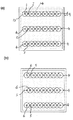
なお、上述の実施例の他に、貫通導体群Gが、一様な距離をもって互いに隣り合うように配置された一例として、図7(a)、(b)に示すように配置することができる。 In addition to the embodiments described above, penetrations conductor group G is, as an example, which is arranged so as to be adjacent to each other with a uniform distance, FIG. 7 (a), the be arranged as shown in (b) it can.
すなわち、第1の貫通導体5と第2の貫通導体6とを直線的に配置し、貫通導体群Gとして、この直線的に配列された貫通導体群Gを一様な距離をもって、互いに平行となるように配置してもよい。ここで、図7(a)と図7(b)との違いは、図7(a)では、例えば、第2の貫通導体6が各列状に配列された貫通導体群Gで、最も左側、3番・・に配列されているのに対して、図7(b)では、第2の貫通導体6が図面の上から1番目と3番目の貫通導体群Gで、最も左側、3番・・に配列され、上から2番目の貫通導体群Gでは、第1の貫通導体5が、最も左側、3番・・に配列されている。
That is, the first through
本発明のコンデンサによれば、2つの第1貫通導体及び2つの第2貫通導体が格子状に配置されて格子の縦横の方向に隣接する第1貫通導体の第1非導体形成領域と第2貫通導体の第2非導体形成領域とが積層方向に重なり合った貫通導体群の複数が、互いに一様な距離をもって配置されているため、貫通導体群内のみに流れる電流は、流れる距離が短くなることから、電流によって誘起される磁束に起因する自己インダクタンス成分が低くなる。このため、コンデンサ全体の等価直列インダクタンス(ESL)を低くできる。また、ESLを低くするために、第1及び第2貫通導体の数を増加する必要がないため、コンデンサの高容量化を実現できる。さらに、貫通導体群間に、貫通導体の無い領域が存在するため、複数の貫通導体群にまたがるように応力が発生することを防止でき、コンデンサのクラックの発生を抑制できる。 According to the capacitor of the present invention, the first non-conductive formation region of the first through-conductor first through conductor and two second through conductors of two adjacent arranged in a grid pattern in the direction of the vertical and horizontal grating and Since a plurality of through conductor groups in which the second non-conductor forming region of the second through conductor overlaps with each other in the stacking direction are arranged at a uniform distance from each other , the current flowing only in the through conductor group is Since it becomes shorter, the self-inductance component caused by the magnetic flux induced by the current becomes lower. For this reason, the equivalent series inductance (ESL) of the whole capacitor can be reduced. Further, since it is not necessary to increase the number of first and second through conductors in order to reduce the ESL, it is possible to realize a high capacity capacitor. Furthermore, since there is a region without through conductors between the through conductor groups, it is possible to prevent stress from being generated across a plurality of through conductor groups and to suppress the occurrence of cracks in the capacitor.
また、貫通導体群を構成し、且つ隣接しあう第1貫通導体と第2貫通導体との間に容量の発生する領域が存在しないため、第1貫通導体から他方、例えば第2貫通導体へ流れる電流は、ほとんど無くなる。このことにより、電流によって誘起される磁束に起因する自己インダクタンス成分が極めて低くなり、コンデンサ全体のESLをさらに低くすることができる。また、第1導体層と第2非導体形成領域、あるいは第2導体層と第1非導体形成領域が重なる部分の面積が減少するため、コンデンサのさらなる高容量化を実現できる。 In addition, since there is no region where a capacitance is generated between the first through conductor and the second through conductor that constitute the through conductor group and are adjacent to each other, the first through conductor flows to the other, for example, the second through conductor. The current is almost gone. As a result, the self-inductance component due to the magnetic flux induced by the current becomes extremely low, and the ESL of the entire capacitor can be further reduced. In addition, since the area of the portion where the first conductor layer and the second non-conductor forming region or the portion where the second conductor layer and the first non-conductor forming region overlap is reduced, it is possible to further increase the capacity of the capacitor.
さらに、第1導体層及び第2導体層の周縁部と貫通導体群の間に、第1貫通導体と第2貫通導体との中心間の間隔P以上の幅で、第1貫通導体、第2貫通導体及び非導体形成領域の無い、静電容量領域が形成されているため、静電容量領域の第1導体層及び第2導体層に流れる電流の量が多くなり、このことによってもコンデンサ全体のESLをさらに効果的に低くすることができる。また、貫通導体群の周囲に静電容量が発生するため、加わる電界を大きくすることができ、このことによってもコンデンサの高容量化を実現できる。 Further, the first through conductor, the second through the first conductor layer and the second conductor layer with a width equal to or greater than the distance P between the centers of the first through conductor and the second through conductor between the peripheral portions of the first conductor layer and the second conductor layer and the through conductor group. Since the capacitance region without the through conductor and non-conductor formation region is formed, the amount of current flowing through the first conductor layer and the second conductor layer in the capacitance region increases, and this also causes the entire capacitor ESL can be further effectively reduced. Further, since electrostatic capacitance is generated around the through conductor group, the applied electric field can be increased, and this also makes it possible to increase the capacity of the capacitor.
またさらに、貫通導体群が、貫通導体及び導体層を流れる電流によって誘起される磁界を互いに相殺するように配置されるため、コンデンサ全体のESLをさらに効果的に低くすることができる。 Furthermore, since the through conductor group is disposed so as to cancel each other out of the magnetic field induced by the current flowing through the through conductor and the conductor layer, the ESL of the entire capacitor can be further effectively reduced.
さらにまた、貫通導体群が、一様な距離をもって互いに隣り合うように配置されるため、貫通導体群間で部分的にESLが高くなることがなく、コンデンサ全体のESLをさらに効果的に低くすることができる。 Furthermore, since the through conductor groups are arranged so as to be adjacent to each other with a uniform distance, the ESL is not partially increased between the through conductor groups, and the ESL of the entire capacitor is further effectively reduced. be able to.
そして、貫通導体群内において、第1及び第2の貫通導体が、実質的に正方形の各頂点に位置する分布状態をもって互いに隣り合うように配置されるため、貫通導体群内で部分的にESLが高くなることがなく、コンデンサ全体のESLをさらに効果的に低くすることができる。 In the through conductor group, the first and second through conductors are arranged so as to be adjacent to each other with a distribution state positioned substantially at each vertex of the square. The ESL of the entire capacitor can be further effectively reduced.
10 コンデンサ
1 積層体
2 誘電体層
3 第1の導体層(内部電極層)
4 第2の導体層(内部電極層)
5 第1の貫通導体(ビアホール導体)
6 第2の貫通導体(ビアホール導体)
13 第1の非導体形成領域
14 第2の非導体形成領域
A 静電容量領域
G 貫通導体群
20 MPU
21 配線基板
22 キャビティ
23 電源側導体層
24 グランド側導体層
40 MPUチップ
37、38 MPUチップの端子
31 マザーボード
10
4 Second conductor layer (internal electrode layer)
5 First through conductor (via hole conductor)
6 Second through conductor (via hole conductor)
13 First
21
Claims (6)
2つの前記第1貫通導体及び2つの前記第2貫通導体が格子状に配置されて格子の縦横の方向に隣接する前記第1貫通導体の前記第1非導体形成領域と前記第2貫通導体の前記第2非導体形成領域とが積層方向に重なり合った貫通導体群を複数形成しているとともに、複数の前記貫通導体群が互いに一様な距離をもって配置され、前記第1導体層及び前記第2導体層の周縁部と前記貫通導体群との間に、前記格子の縦横の方向に隣接する前記第1貫通導体と前記第2貫通導体との中心間の間隔以上の幅で、前記第1導体層及び前記第2導体層が存在していることを特徴とするコンデンサ。 The first conductor layer is disposed on one main surface of the dielectric layer, the second conductor layer is disposed on the other main surface of the dielectric layer, and the second conductor layer and the second conductor layer are disposed in the thickness direction of the dielectric layer. A plurality of first through conductors separated by one non-conductor formation region and connected to the first conductor layer; and separated by the first conductor layer and the second non-conductor formation region; and In a capacitor formed with a plurality of second through conductors to be connected,
The two first through conductors and the two second through conductors are arranged in a lattice shape, and the first non-conductor forming region of the first through conductor and the second through conductor adjacent to each other in the vertical and horizontal directions of the lattice. A plurality of through conductor groups in which the second non-conductor forming region overlaps in the stacking direction are formed, and the plurality of through conductor groups are arranged at a uniform distance from each other, and the first conductor layer and the second conductor group between the through conductor group and the peripheral portion of the conductor layer, at intervals over the width between the centers of said first through conductor and the second through-conductor adjacent to the longitudinal and lateral directions of the grating, the first conductor A capacitor, wherein a layer and the second conductor layer are present.
Priority Applications (1)
| Application Number | Priority Date | Filing Date | Title |
|---|---|---|---|
| JP2003335812A JP4931329B2 (en) | 2002-09-27 | 2003-09-26 | Capacitor, wiring board, decoupling circuit and high frequency circuit |
Applications Claiming Priority (3)
| Application Number | Priority Date | Filing Date | Title |
|---|---|---|---|
| JP2002284379 | 2002-09-27 | ||
| JP2002284379 | 2002-09-27 | ||
| JP2003335812A JP4931329B2 (en) | 2002-09-27 | 2003-09-26 | Capacitor, wiring board, decoupling circuit and high frequency circuit |
Related Child Applications (1)
| Application Number | Title | Priority Date | Filing Date |
|---|---|---|---|
| JP2006076660A Division JP2006222441A (en) | 2002-09-27 | 2006-03-20 | Capacitor, wiring board, decoupling circuit, and high-frequency circuit |
Publications (3)
| Publication Number | Publication Date |
|---|---|
| JP2004140351A JP2004140351A (en) | 2004-05-13 |
| JP2004140351A5 JP2004140351A5 (en) | 2006-05-11 |
| JP4931329B2 true JP4931329B2 (en) | 2012-05-16 |
Family
ID=32473225
Family Applications (1)
| Application Number | Title | Priority Date | Filing Date |
|---|---|---|---|
| JP2003335812A Expired - Fee Related JP4931329B2 (en) | 2002-09-27 | 2003-09-26 | Capacitor, wiring board, decoupling circuit and high frequency circuit |
Country Status (1)
| Country | Link |
|---|---|
| JP (1) | JP4931329B2 (en) |
Families Citing this family (2)
| Publication number | Priority date | Publication date | Assignee | Title |
|---|---|---|---|---|
| JP5404312B2 (en) * | 2009-07-29 | 2014-01-29 | 京セラ株式会社 | Electronic equipment |
| WO2016067746A1 (en) * | 2014-10-30 | 2016-05-06 | 日立オートモティブシステムズ株式会社 | Laminated capacitor and in-vehicle control device |
-
2003
- 2003-09-26 JP JP2003335812A patent/JP4931329B2/en not_active Expired - Fee Related
Also Published As
| Publication number | Publication date |
|---|---|
| JP2004140351A (en) | 2004-05-13 |
Similar Documents
| Publication | Publication Date | Title |
|---|---|---|
| US8410887B2 (en) | Built-in-coil substrate | |
| JP2020057754A (en) | Multilayer ceramic electronic component | |
| KR101504015B1 (en) | Multi-layered ceramic capacitor and mounting circuit board thereof | |
| KR20150018140A (en) | Embedded multilayer ceramic electronic part and print circuit board having embedded multilayer ceramic electronic part | |
| KR20170087665A (en) | Multi-layered ceramic capacitor and board for mounting the same | |
| KR102097324B1 (en) | Multi-layered ceramic capacitor and board for mounting the same | |
| KR20140081360A (en) | Multi-layered ceramic capacitor, manufacturing method of the same and circuit board for mounting the same | |
| JP2015076600A (en) | Multilayer ceramic electronic component to be embedded in board and multilayer ceramic electronic component embedded printed circuit board | |
| JPH04220004A (en) | Voltage controlled oscillator | |
| KR101832611B1 (en) | Multi-layered capacitor and board for mounting the same | |
| KR101489815B1 (en) | Multi-layered ceramic capacitor | |
| JP2006222441A (en) | Capacitor, wiring board, decoupling circuit, and high-frequency circuit | |
| JP2004296936A (en) | Ceramic electronic component | |
| JP2016086150A (en) | Multilayer ceramic capacitor | |
| JP4458812B2 (en) | Capacitor, capacitor manufacturing method, wiring board, decoupling circuit, and high-frequency circuit | |
| KR20150018137A (en) | Embedded multilayer ceramic electronic part and print circuit board having embedded multilayer ceramic electronic part | |
| JP2021097202A (en) | Multilayer capacitor and mounting board thereof | |
| KR102037268B1 (en) | Multi layered ceramic capacitor and board having the same mounted thereon | |
| JP2017120876A (en) | Multilayer electronic component and method of manufacturing the same | |
| JP4931329B2 (en) | Capacitor, wiring board, decoupling circuit and high frequency circuit | |
| KR102449360B1 (en) | Multilayered ceramic capacitor and board having the same mounted thereon | |
| JP2004140350A (en) | Capacitor, wiring board, decoupling circuit, and high-frequency circuit | |
| JP2005203623A (en) | Capacitor, manufacturing method thereof, wiring board, decoupling circuit, and high frequency circuit | |
| JPH0817675A (en) | Chip type laminated ceramic capacitor | |
| JP2006222442A (en) | Capacitor and wiring board |
Legal Events
| Date | Code | Title | Description |
|---|---|---|---|
| A521 | Written amendment |
Free format text: JAPANESE INTERMEDIATE CODE: A523 Effective date: 20060320 |
|
| A621 | Written request for application examination |
Free format text: JAPANESE INTERMEDIATE CODE: A621 Effective date: 20060912 |
|
| A131 | Notification of reasons for refusal |
Free format text: JAPANESE INTERMEDIATE CODE: A131 Effective date: 20090120 |
|
| A521 | Written amendment |
Free format text: JAPANESE INTERMEDIATE CODE: A523 Effective date: 20090319 |
|
| A02 | Decision of refusal |
Free format text: JAPANESE INTERMEDIATE CODE: A02 Effective date: 20091201 |
|
| A521 | Written amendment |
Free format text: JAPANESE INTERMEDIATE CODE: A523 Effective date: 20111217 |
|
| A01 | Written decision to grant a patent or to grant a registration (utility model) |
Free format text: JAPANESE INTERMEDIATE CODE: A01 |
|
| A61 | First payment of annual fees (during grant procedure) |
Free format text: JAPANESE INTERMEDIATE CODE: A61 Effective date: 20120214 |
|
| R150 | Certificate of patent or registration of utility model |
Free format text: JAPANESE INTERMEDIATE CODE: R150 |
|
| FPAY | Renewal fee payment (event date is renewal date of database) |
Free format text: PAYMENT UNTIL: 20150224 Year of fee payment: 3 |
|
| LAPS | Cancellation because of no payment of annual fees |