JP4931231B2 - Imaging apparatus and control method thereof - Google Patents
Imaging apparatus and control method thereof Download PDFInfo
- Publication number
- JP4931231B2 JP4931231B2 JP2007166688A JP2007166688A JP4931231B2 JP 4931231 B2 JP4931231 B2 JP 4931231B2 JP 2007166688 A JP2007166688 A JP 2007166688A JP 2007166688 A JP2007166688 A JP 2007166688A JP 4931231 B2 JP4931231 B2 JP 4931231B2
- Authority
- JP
- Japan
- Prior art keywords
- pixels
- voltage
- imaging apparatus
- pixel
- transfer switch
- Prior art date
- Legal status (The legal status is an assumption and is not a legal conclusion. Google has not performed a legal analysis and makes no representation as to the accuracy of the status listed.)
- Expired - Fee Related
Links
Images


Description
本発明は、CMOSイメージセンサ等の撮像素子を用いた撮像装置及びその制御方法に関する。 The present invention relates to an imaging apparatus using an imaging element such as a CMOS image sensor and a control method thereof .
デジタルカメラやビデオカメラ等の撮像装置においては、撮像素子としてCCDやCMOSイメージセンサを使用するのが一般的である。近年、撮像素子の多画素化が進む一方で、一定の面積内に数万もの画素を構成させるため、画素サイズは極度に縮小してきている。このため、1画素当たりが集光できる光量が減少すると共に、1画素当たりの飽和光量も極度に減少している。つまり、このような撮像装置で高コントラストの被写体を撮影した場合、明るい部分ではすぐに白飛び現象が発生してしまう。 In an imaging apparatus such as a digital camera or a video camera, a CCD or a CMOS image sensor is generally used as an imaging element. In recent years, while the number of pixels of an image sensor has been increased, the pixel size has been extremely reduced in order to form tens of thousands of pixels within a certain area. For this reason, the amount of light that can be collected per pixel is reduced, and the amount of saturated light per pixel is also extremely reduced. That is, when a high-contrast subject is photographed with such an imaging apparatus, a whiteout phenomenon occurs immediately in a bright part.
このような点から、イメージセンサの飽和防止、つまりは飽和画素を検出して全画素の電荷蓄積動作を停止させる技術については、種々の提案がされている(例えば、特許文献1参照)。 In view of this point, various proposals have been made on the technology for preventing saturation of the image sensor, that is, a technique for detecting the saturated pixels and stopping the charge accumulation operation of all the pixels (see, for example, Patent Document 1).
特許文献1では、測距用のラインセンサにおいて1つのラインを構成する画素の中からピーク出力画素が所定のレベルに達することを検出し、電荷蓄積動作を停止させようとするものである。また、複数ラインセンサがある場合は、ライン毎のピーク出力画素を時系列に検出することで、複数ラインに適用している。
しかしながら、上記特許文献1の手法を2次元の撮像素子を有する撮像装置に適用する場合、行又は列毎に時系列にピーク出力画素の検出を行うことになるため、リアルタイムに電荷蓄積動作の停止などの制御を行うことができないという問題があった。
However, when the technique of
本発明は上記従来の問題点に鑑み、以下を目的とする撮像装置及びその画素飽和状態検出方法を提供する。即ち、白飛び現象の無い良好な画像を得るために、撮像素子における画素の飽和状態をリアルタイムに検出して、電荷蓄積動作の停止などの制御をリアルタイムに行うことができることを目的とする。 In view of the above-described conventional problems, the present invention provides an imaging apparatus and a pixel saturation state detection method for the following purpose. In other words, in order to obtain a good image without a whiteout phenomenon, it is an object of the present invention to detect in real time the saturation state of the pixels in the image sensor and to perform control such as stopping the charge accumulation operation in real time.
上記目的を達成するため、本発明の撮像装置は、複数の画素が配列された撮像素子を有する撮像装置において、前記複数の画素にリセット電圧を供給するための共通電源と、前記共通電源に流れる電流に基づいて前記複数の画素のいずれかが飽和状態にあることを検出する飽和検出手段と、を有することを特徴とする。 In order to achieve the above object, an imaging apparatus according to the present invention includes an imaging device having an imaging element in which a plurality of pixels are arranged, and a common power source for supplying a reset voltage to the plurality of pixels and the common power source. any of the plurality of pixels based on current and having a saturated detecting means for detecting that saturation.
また、本発明の撮像装置の制御方法は、複数の画素が配列され、前記複数の画素にリセット電圧を供給するための共通電源を備えた撮像素子を有する撮像装置の制御方法であって、前記共通電源に流れる電流に基づいて前記複数の画素のいずれかが飽和状態にあることを検出することを特徴とする。 The control method of the image pickup apparatus of the present invention, pixels in multiple are arranged, there is provided a control method for an image pickup apparatus having an image pickup element having a common power supply for supplying a reset voltage to the plurality of pixels, It is detected that any of the plurality of pixels is in a saturated state based on a current flowing through the common power source .
本発明によれば、撮像素子における画素の飽和状態をリアルタイムに検出して、電荷蓄積動作の停止などの制御をリアルタイムに行うことが可能になる。これにより、撮影した画像の白飛び現象を確実に防止することができ、画質を向上を図ることができる。 According to the present invention, it is possible to detect in real time the saturation state of the pixels in the image sensor and perform control such as stopping the charge accumulation operation in real time. As a result, it is possible to reliably prevent the whiteout phenomenon of the photographed image and improve the image quality.
以下、本発明の実施の形態について、図面を参照しながら説明する。 Hereinafter, embodiments of the present invention will be described with reference to the drawings.
<実施の形態に係る画素部回路の構成>
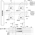
図1は、本発明の実施の形態に係る撮像装置の要部構成を示す回路図であり、光電変換用の撮像素子としてCMOS型エリアセンサを用いた画素部回路を示している。
<Configuration of Pixel Circuit According to Embodiment>
FIG. 1 is a circuit diagram showing a main configuration of an image pickup apparatus according to an embodiment of the present invention, and shows a pixel portion circuit using a CMOS area sensor as an image pickup element for photoelectric conversion.
撮像素子は、複数の画素内の光量電荷を蓄積して電気信号として出力する。画素部回路は、駆動パルスが入力される駆動パルス入力線12と、信号が出力される垂直出力線13とがマトリックス状に配列されている。
The image sensor accumulates light quantity charges in a plurality of pixels and outputs them as electric signals. In the pixel unit circuit, drive
駆動パルス入力線12は、駆動パルスとしてPselパルス、Presパルス及びPtxパルスがそれぞれ供給される3本の信号線から成る。駆動パルス入力線12と垂直出力線13との各交差箇所には、それぞれ光電変換用の画素50が接続され、各駆動パルス入力線12は、垂直走査回路14に接続されている。
The drive
以下、(m+1)行目の駆動パルスは、Pres(m+1)パルス、Ptx(m+1)パルス、Psel(m+1)パルスと記し、(m)行目の駆動パルスは、Pres(m)パルス、Ptx(m)パルス、Psel(m)パルスと記す。また、(m+1)行目の画素は画素50(m+1)と記し、(m)行目の画素は画素50(m)と記す。さらに、(m+1)行目の駆動パルス入力線は、駆動パルス入力線12(m+1)と記し、(m)行目の駆動パルス入力線は、駆動パルス入力線12(m)と記す。そして、(n+1)列目の垂直出力線は、垂直出力線13(n+1)と記し、(n)列目の垂直出力線は、垂直出力線13(n)と記す。 Hereinafter, the driving pulse in the (m + 1) th row is referred to as a Pres (m + 1) pulse, a Ptx (m + 1) pulse, and a Psel (m + 1) pulse, and the driving pulse in the (m) row is a Pres (m) pulse, Ptx ( m) Pulse and Psel (m) pulse. The pixel in the (m + 1) th row is denoted as a pixel 50 (m + 1), and the pixel in the (m) th row is denoted as a pixel 50 (m). Further, the drive pulse input line in the (m + 1) th row is denoted as drive pulse input line 12 (m + 1), and the drive pulse input line in the (m) th row is denoted as drive pulse input line 12 (m). The vertical output line in the (n + 1) th column is denoted as a vertical output line 13 (n + 1), and the vertical output line in the (n) th column is denoted as a vertical output line 13 (n).
垂直走査回路14は、所定の行の画素50を選択する。この選択行の画素50の出力が垂直出力線13(m+1)、(m)、…下に読み出され、各転送ゲート15a,15bを介して、信号蓄積部15に蓄積される。信号蓄積部15に蓄積された出力は水平走査回路16によって順次出力アンプ部へ読み出されるようになっている。
The
図2は、図1中の画素50の回路構成を示す回路図である。
FIG. 2 is a circuit diagram showing a circuit configuration of the
この各画素50(m)、(m+1)、…は、同一の回路構成である。即ち、各画素50は、NチャネルMOSトランジスタ(以下、単にMOSトランジスタと記す)から成るリセットスイッチ3を有する。また、リセットスイッチ3と電源SVDD(共通電源)との間には、電源SVDDに流れ込む電流をモニタするためのMOSトランジスタ21が接続されている。そして、そのMOSトランジスタ21のゲートを共通ゲートとするMOSトランジスタ22を設けてカレントミラー回路が構成されている。
Each of the pixels 50 (m), (m + 1),... Has the same circuit configuration. That is, each
MOSトランジスタ22のドレインは電源SVDDに接続され、ソースは負荷抵抗23を介して接地されている。さらに、前記カレントミラー回路の出力としてMOSトランジスタ22のソースは、可変電源Vcompを閾値とするコンパレータ24の入力側に接続され、コンパレータ24の出力側からVsvddmon信号が出力される。つまり、電源SVDDに流れる電流変化により、前記カレントミラー回路の出力電圧が所定電圧(Vcomp)を越えた場合にVsvddmon信号として出力される構成(飽和検出手段)となっている。
The drain of the
リセットスイッチ3のソースと接地との間には、接続点Nを介して、フローティングデフュージョン(FD)と呼ばれる電荷蓄積部9(以下、FD部9と記す)が接続されている。さらに、接続点Nと接地との間には、MOSトランジスタから成るMOS型転送スイッチ2と、光電変換用のフォトダイオード(PD)1とが直列接続されている。転送スイッチ2のゲートは、可変電圧バッファ18の出力側に接続されている。可変電圧バッファ18は、転送パルスPtxを入力し、転送スイッチ2のゲートに印加する低レベル電圧(Vtxl)を可変にするためのバッファである。
A charge storage unit 9 called a floating diffusion (FD) (hereinafter referred to as FD unit 9) is connected between the source of the
また、リセットスイッチ3のドレインと、当該画素50の出力端である垂直出力線13との間には、MOSトランジスタから成る行選択スイッチ6と、MOSトランジスタから成る画素アンプ10とが直列接続されている。画素アンプ10と負荷電流源7とでソース・フォロア回路が構成されている。そして、行選択スイッチ6のゲートは、行選択用の駆動パルスPselが印加され、画素アンプ10のゲートには、前記接続点Nが接続される。
A
図2の回路によれば、光電変換はPD1で行われ、光量電荷の蓄積期間中は、転送スイッチ2はオフ状態であり、画素アンプ10のゲート、即ちFD部9にはこのPD1で光電変換された電荷は転送されない。画素アンプ10のゲートは、蓄積開始前に該リセットスイッチ3がオンし、適当な電圧に初期化されている。即ちこれがダークレベルとなる。
According to the circuit of FIG. 2, photoelectric conversion is performed by
次に又は同時に行選択スイッチ6がオンになると、負荷電流源7と画素アンプ10で構成されるソース・フォロア回路が動作状態になり、このとき、該転送スイッチ2をオンさせることでPD1に蓄積されていた電荷は、画素アンプ10のゲートに転送される。
Next or simultaneously, when the
ここで、選択行の画素の出力が図1の垂直出力線13上に発生する。この出力は、各転送ゲート15a,15bを介して、信号蓄積部15に蓄積される。信号蓄積部15に一時蓄積された出力は水平走査回路16によって順次出力アンプ部へ読み出される。
Here, the output of the pixel in the selected row is generated on the
なお、前記カレントミラー回路及びコンパレータ24を含む構成を図2に示すように画素毎に配置することもできるが、回路が複雑になり回路構成面積も膨大になるため、行毎或いは列毎、又は全画素共通で1つの構成とすることも可能である。以下の本実施の形態における説明では、説明を簡単にするために、前記カレントミラー回路及びコンパレータ24を含む構成を、全画素共通で1つの構成とする前提で説明する。
The configuration including the current mirror circuit and the
<本実施の形態に係る撮像装置の動作>
次に、図3等を参照して、本実施の形態に係る撮像装置の動作を詳細に説明する。
<Operation of Imaging Device According to this Embodiment>
Next, with reference to FIG. 3 etc., operation | movement of the imaging device which concerns on this Embodiment is demonstrated in detail.
図3は、本実施の形態に係る撮像装置の動作を示すタイミングチャートである。 FIG. 3 is a timing chart showing the operation of the imaging apparatus according to the present embodiment.
図中のPVSRパルスは、垂直転送パルスであり、PHSRパルスは水平転送パルスである。メカニカルシャッタ(以下、メカシャッタと記す)は、開閉することで撮像素子の露光時間を制御する。VPD(m+1,n)は、(m+1)行、(n)列のフォトダイオード1の出力電圧であり、VFD(m+1,n)は、(m+1)行、(n)列の画素アンプ10のゲート電圧である。ITres(m+1,n)は、(m+1)行、(n)列のリセットスイッチ3を流れる電流である。
The PVSR pulse in the figure is a vertical transfer pulse, and the PHSR pulse is a horizontal transfer pulse. A mechanical shutter (hereinafter referred to as a mechanical shutter) controls the exposure time of the image sensor by opening and closing. VPD (m + 1, n) is the output voltage of the
図3のA時点において、Presパルスを“1”にすることで、リセットスイッチ3をオン状態にしてFD部9をSVDD電圧でリセットする(図3のT1)。その状態で更にPtxパルスを“1”にすることで、転送スイッチ2をオンしてPD1をリセットし(T2)、更にPtxパルスを“0”にすることで、転送スイッチ2をオフしてPD1の蓄積を開始する。ここまでの動作は、全行一括で行われる。
At time A in FIG. 3, by setting the Pres pulse to “1”, the
その後、メカシャッタを開閉させて画素部を露光させる(T3)。露光終了後、Pres(m+1)パルスを“0”にすることでリセットスイッチ3をオフして、(m+1)行目のFD部9のリセット解除を行う。さらに、Psel(m+1)パルスを“1”にすることで(T4)、(m+1)行目の行選択スイッチ6をオンし、(m+1)行目の画素アンプ10の出力が垂直出力線13に接続される(この状態を仮に状態K1とする)。
Thereafter, the mechanical shutter is opened and closed to expose the pixel portion (T3). After the exposure is completed, the
そして、Ptx(m+1)パルスを“1”にすることで(T5)、(m+1)行目の転送スイッチ2をオンさせて、PD1で蓄積された光量電荷をFD部9へ転送する。そして、この光量電荷が、画素アンプ10を介して垂直出力線13に読み出される(この状態を仮に状態K2とする)。このとき、状態K1の出力と状態K2の出力を画素毎に一時記憶し、その差分をとることで各画素の出力を得ることができる。
Then, by setting the Ptx (m + 1) pulse to “1” (T5), the
その後、Ptx(m+1)パルスを“0”にすることで(T6)転送スイッチ2をオフさせる。さらに、Pres(m+1)パルスを“1”、Ptx(m+1)パルスを“1”、Psel(m+1)パルスを“0”にすることで(T7)、(m+1)行目の垂直出力線13への出力をオフさせ、FD部9及びPD1をリセットさせる。
After that, the
その後、画素毎に記憶された信号を、水平転送パルスPHSRを駆動することで逐次読み出し(T8)、その読み出し終了後に、垂直転送パルスPVSRを駆動することで(T9)、次の(m)行の読み出しに移行する。(m)行の読み出し動作も、前記(m+1)行目の動作と等価なので説明を省略する。 Thereafter, the signals stored for each pixel are sequentially read by driving the horizontal transfer pulse PHSR (T8), and after the reading is completed, the vertical transfer pulse PVSR is driven (T9), and the next (m) row. Move on to reading. The operation of reading out the (m) row is equivalent to the operation of the (m + 1) th row, and the description thereof will be omitted.
ここで、PD1の電圧VPD(m+1,n)は、リセット後にメカシャッタが開状態になった瞬間(T3)からPD1に光量電荷が蓄積されるため、徐々に低下していくが、PD1が飽和したところで(T10)、その電圧降下は停止する。 Here, the voltage VPD (m + 1, n) of PD1 gradually decreases because the light amount charge is accumulated in PD1 from the moment (T3) when the mechanical shutter is opened after reset, but PD1 is saturated. By the way (T10), the voltage drop stops.
一方、PD1が飽和後、光量電荷はPD1の周辺に溢れて半導体基板方向に吸収される。また、その一部はオフ状態の転送スイッチ2を越えてリセットスイッチ3を介して、電源SVDDへ流れ込む。このとき、FD部9は、低インピーダンスの電源SVDDでリセットされているため、その電圧変化は無いが、リセットスイッチ3を介して電源SVDDに流れる電流は増加する。
On the other hand, after PD1 is saturated, the light charge overflows around PD1 and is absorbed toward the semiconductor substrate. Further, a part thereof flows into the power supply SVDD through the
このような点を考慮して、本実施の形態では、PD1の飽和状態を検出する方法として、蓄積中の電源SVDDに流れる電流をモニタする方法を採用している。即ち、全画素共通の電源SVDDに流れ込む電流を例えば全画素共通の1つのカレントミラー回路を介してモニタし、全画素中のどこかの画素が飽和したところでその飽和状態を検出する。画素の飽和状態を検出したらメカシャッタを閉じ、これによって画素部に対する露光を停止させるように構成している。 In consideration of such points, in the present embodiment, as a method of detecting the saturation state of PD1, a method of monitoring the current flowing through the power supply SVDD during storage is employed. That is, the current flowing into the power supply SVDD common to all the pixels is monitored through, for example, one current mirror circuit common to all the pixels, and the saturated state is detected when any pixel in all the pixels is saturated. When the saturation state of the pixel is detected, the mechanical shutter is closed, and thereby the exposure to the pixel portion is stopped.
また、転送スイッチ2のゲートには、PD1の蓄積電荷のFD部9へのリークを防止するため、−1.2V程度(第2の電圧)の低い電圧を印加することで転送スイッチを強力にオフさせるのが一般的である。しかし、本実施の形態では、PD1の飽和状態を精度よく検出させるために、可変電圧バッファ18により、PD1の蓄積動作中のみ転送スイッチ2のオフ時のゲート電圧を−0.8V程度(第1の電圧)にする。これにより、PD1が飽和した後の電荷を極力転送スイッチ2の方向に溢れさせるように工夫している。
Further, in order to prevent the accumulated charge of PD1 from leaking to the FD section 9, a low voltage of about −1.2 V (second voltage) is applied to the gate of the
しかし、転送スイッチ2に印加する低レベル電圧は、より低くすることで転送スイッチ2を強力にオフさせる効果があるとともに、転送スイッチ2のゲート下の暗電流を抑制する効果もある。従って、この低レベル電圧を画素部の蓄積動作中に上げると、より多くの暗電流を発生してしまうことになる。
However, lowering the low-level voltage applied to the
この対策として、暗電流が無視できないような撮影条件、例えば、露光時間或いは電荷蓄積時間が長い場合や、環境温度が高温の場合は、次のようにしても良い。即ち、低レベル電圧を−0.8V(第1の電圧)よりも若干低め(例えば−0.9V:第3の電圧)にコントロールする。 As a countermeasure, the following may be performed under photographing conditions in which the dark current cannot be ignored, for example, when the exposure time or charge accumulation time is long, or when the environmental temperature is high. That is, the low level voltage is controlled to be slightly lower than −0.8 V (first voltage) (for example, −0.9 V: third voltage).
また、露光が終了してから信号読み出しまでにタイムラグが生じる場合、露光終了後に発生する暗電流分も無視できない。このため、露光終了後には、転送スイッチ2に印加される低レベル電圧を、更に低い電圧(例えば、−1.2V:第2の電圧)にするようにしている。これにより、撮影された画像のほとんどの領域は飽和の無い、階調を残した画像として得ることができる。
Also, when a time lag occurs between the end of exposure and the signal readout, the dark current generated after the end of exposure cannot be ignored. For this reason, after the exposure is completed, the low level voltage applied to the
次に、本実施の形態に係る画素部回路の特徴を明確化するために、一般的な従来回路と対比して説明する。 Next, in order to clarify the characteristics of the pixel portion circuit according to this embodiment, a description will be given in comparison with a general conventional circuit.
図4は、図2に対応した従来の一般的な画素の回路図であり、図2と共通の要素には同一の符号を付し、その説明を省略する。また、図5は、図4の従来の画素の回路の動作を示すフローチャートであり、図3と共通の要素には同一の符号を付し、その説明を省略する。 FIG. 4 is a circuit diagram of a conventional general pixel corresponding to FIG. 2. Elements common to FIG. 2 are denoted by the same reference numerals, and description thereof is omitted. FIG. 5 is a flowchart showing the operation of the circuit of the conventional pixel in FIG. 4. Elements common to those in FIG.
図4に示すように、従来の一般的な画素の回路は、図2で示した本実施の形態に係る画素の回路において、カレントミラー回路と可変電圧バッファ18を除いた構成になっている。この点から明らかなように、本実施の形態における画素の回路の特徴は、カレントミラー回路を設けてコンパレータ24から前記Vsvddmon信号を出力する構成にした。さらに、可変電圧バッファ18を設けて転送スイッチ2のゲートに低レベル電圧Vtxlを印加するように構成した点である。
As shown in FIG. 4, the conventional general pixel circuit has a configuration in which the current mirror circuit and the
転送スイッチ2のゲートに印加する低レベル電圧(Vtxl)は、本実施の形態では、メカシャッタの開時間に同期して−0.8V(第1の電圧)にしている(図3のT11)。このため、PD1の飽和後にリセットスイッチ3に流れる電流は、図5に示す従来回路と比べて大きくなる(図3のT12と図5のT22参照)。この電流によって適切な閾値電圧(Vcomp)に設定されたコンパレータ24の出力がVsvddmon信号として出力される(図3のT13)。
In the present embodiment, the low level voltage (Vtxl) applied to the gate of the
<本実施の形態の利点>
(1)本実施の形態によれば、光量電荷の蓄積中にVsvddmon信号をモニタして、その出力値が1になったことを検出することにより、全画素内のいずれかの画素が飽和したものとして、メカシャッタを閉じて露光を停止する。このような画素の飽和による露光停止(蓄積動作の停止)の制御をリアルタイムに行うことができる。即ち、全画素中のいずれかの画素が飽和しているかどうかをリアルタイムに検出することができ、その結果により露光又は蓄積を停止させる。そのため、飽和画素の極めて少ない画像を得ることができ、白飛び現象の無い且つ階調性を損なわない画像を得ることが可能となる。
<Advantages of this embodiment>
(1) According to the present embodiment, any pixel in all the pixels is saturated by monitoring the Vsvddmon signal during the accumulation of the light amount charge and detecting that the output value becomes 1. As a thing, the mechanical shutter is closed to stop the exposure. Such exposure stop (accumulation of storage operation) control due to pixel saturation can be controlled in real time. That is, it is possible to detect in real time whether any of the pixels is saturated, and the exposure or accumulation is stopped according to the result. Therefore, an image with very few saturated pixels can be obtained, and an image with no whiteout phenomenon and no deterioration in gradation can be obtained.
(2)転送スイッチ2のゲートに印加される低レベル電圧(Vtxl)を、露光中又は光量電荷の蓄積中には通例よりも若干高い電圧(例えば−0.8V)に設定し、それ以外の時は若干低い電圧(例えば−1.2V)にするようにした。これにより、暗電流による悪影響を少なくすることができる。
(2) The low level voltage (Vtxl) applied to the gate of the
(3)更に、露光中又は光量電荷蓄積中に転送スイッチ2のゲートに印加される低レベル電圧(Vtxl)を、露光時間又は蓄積時間、或いは周囲環境温度に合わせて可変にすることにより、更に暗電流の悪影響を排除することができる。
(3) Further, by changing the low level voltage (Vtxl) applied to the gate of the
なお、上記の説明では、露光時間の制御をメカシャッタを用いて行うようにしているが、露光時間の制御を一般にいわれる電子シャッタにより行うことができる場合は、その方法を用いて露光制御させても良い。 In the above description, the exposure time is controlled using a mechanical shutter. However, if the exposure time can be controlled by an electronic shutter that is generally referred to, exposure control is performed using that method. Also good.
1 フォトダイオード
2 転送スイッチ
3 リセットスイッチ
6 行選択スイッチ
9 フローティングデフュージョン
10 画素アンプ
13 垂直出力線
14 垂直走査回路
16 水平走査回路
18 可変電圧バッファ
21、22 MOSトランジスタ
23 負荷抵抗
24 コンパレータ
DESCRIPTION OF
Claims (7)
前記複数の画素にリセット電圧を供給するための共通電源と、
前記共通電源に流れる電流に基づいて前記複数の画素のいずれかが飽和状態にあることを検出する飽和検出手段と、
を有することを特徴とする撮像装置。 In an imaging device having an imaging element in which a plurality of pixels are arranged ,
A common power supply for supplying a reset voltage to the plurality of pixels ;
A saturation detection means for said one of the plurality of pixels based on the current flowing through the common power supply is detected to be in a saturated state,
An imaging device comprising:
前記共通電源に流れる電流に基づいて前記複数の画素のいずれかが飽和状態にあることを検出することを特徴とする撮像装置の制御方法。 Pixels multiple are arranged, a control method of an image pickup apparatus having an image pickup element having a common power supply for supplying a reset voltage to said plurality of pixels,
A method for controlling an imaging apparatus, comprising: detecting that any of the plurality of pixels is in a saturated state based on a current flowing through the common power source .
Priority Applications (1)
| Application Number | Priority Date | Filing Date | Title |
|---|---|---|---|
| JP2007166688A JP4931231B2 (en) | 2007-06-25 | 2007-06-25 | Imaging apparatus and control method thereof |
Applications Claiming Priority (1)
| Application Number | Priority Date | Filing Date | Title |
|---|---|---|---|
| JP2007166688A JP4931231B2 (en) | 2007-06-25 | 2007-06-25 | Imaging apparatus and control method thereof |
Publications (3)
| Publication Number | Publication Date |
|---|---|
| JP2009005285A JP2009005285A (en) | 2009-01-08 |
| JP2009005285A5 JP2009005285A5 (en) | 2010-08-05 |
| JP4931231B2 true JP4931231B2 (en) | 2012-05-16 |
Family
ID=40321146
Family Applications (1)
| Application Number | Title | Priority Date | Filing Date |
|---|---|---|---|
| JP2007166688A Expired - Fee Related JP4931231B2 (en) | 2007-06-25 | 2007-06-25 | Imaging apparatus and control method thereof |
Country Status (1)
| Country | Link |
|---|---|
| JP (1) | JP4931231B2 (en) |
Families Citing this family (3)
| Publication number | Priority date | Publication date | Assignee | Title |
|---|---|---|---|---|
| JP5266884B2 (en) | 2008-05-30 | 2013-08-21 | ソニー株式会社 | Solid-state imaging device, imaging device, and pixel driving method |
| JP6452241B2 (en) * | 2015-02-13 | 2019-01-16 | セイコーNpc株式会社 | Image sensor |
| JP2018019354A (en) * | 2016-07-29 | 2018-02-01 | キヤノン株式会社 | Imaging apparatus |
Family Cites Families (4)
| Publication number | Priority date | Publication date | Assignee | Title |
|---|---|---|---|---|
| JPH01103378A (en) * | 1987-10-16 | 1989-04-20 | Sanyo Electric Co Ltd | Exposure control circuit for solid-state image pickup element |
| JP2006197425A (en) * | 2005-01-17 | 2006-07-27 | Sony Corp | Solid-state image pickup device, method for driving solid-state image pickup device, and image pickup device |
| JP4743839B2 (en) * | 2005-02-15 | 2011-08-10 | キヤノン株式会社 | Imaging device |
| JP4696877B2 (en) * | 2005-11-29 | 2011-06-08 | ヤマハ株式会社 | Solid-state imaging device |
-
2007
- 2007-06-25 JP JP2007166688A patent/JP4931231B2/en not_active Expired - Fee Related
Also Published As
| Publication number | Publication date |
|---|---|
| JP2009005285A (en) | 2009-01-08 |
Similar Documents
| Publication | Publication Date | Title |
|---|---|---|
| US6452633B1 (en) | Exposure control in electronic cameras by detecting overflow from active pixels | |
| JP4185949B2 (en) | Photoelectric conversion device and imaging device | |
| JP5247007B2 (en) | Imaging apparatus and imaging system | |
| US9030589B2 (en) | Image sensor and image sensing apparatus | |
| KR101435964B1 (en) | Imaging device and driving method for solid-state image sensor | |
| JP6353533B2 (en) | Solid-state imaging device and electronic information device | |
| US8212905B2 (en) | Photoelectric conversion device, imaging system, and photoelectric conversion device driving method | |
| US20040130757A1 (en) | Solid-state imaging device and control method for same | |
| US8384006B2 (en) | Image pickup apparatus | |
| US8223240B2 (en) | Image pickup device and image pickup apparatus | |
| US20150281610A1 (en) | Solid-state imaging apparatus and imaging system | |
| US20050128324A1 (en) | Image sensing apparatus and method of controlling same | |
| JP4300635B2 (en) | Solid-state imaging device | |
| JP4758318B2 (en) | Solid-state imaging device | |
| JP4931231B2 (en) | Imaging apparatus and control method thereof | |
| US20040189845A1 (en) | Solid-state image sensing apparatus | |
| US8294799B2 (en) | Solid-state imaging apparatus | |
| US7999871B2 (en) | Solid-state imaging apparatus, and video camera and digital still camera using the same | |
| JP5627728B2 (en) | Imaging apparatus and imaging system | |
| JP2008042675A (en) | Photoelectric conversion device and imaging apparatus | |
| JP2006262070A (en) | Photoelectric transducer and coms image sensor | |
| JP2013197697A (en) | Solid-state image pickup device and electronic apparatus | |
| US8098315B2 (en) | Solid state imaging apparatus, solid state imaging device driving method and camera | |
| JP2007214791A (en) | Imaging element, imaging apparatus, and driving method of imaging element | |
| US7978243B2 (en) | Imaging apparatus, driving method thereof, and imaging system |
Legal Events
| Date | Code | Title | Description |
|---|---|---|---|
| A521 | Request for written amendment filed |
Free format text: JAPANESE INTERMEDIATE CODE: A523 Effective date: 20100622 |
|
| A621 | Written request for application examination |
Free format text: JAPANESE INTERMEDIATE CODE: A621 Effective date: 20100622 |
|
| A977 | Report on retrieval |
Free format text: JAPANESE INTERMEDIATE CODE: A971007 Effective date: 20120113 |
|
| TRDD | Decision of grant or rejection written | ||
| A01 | Written decision to grant a patent or to grant a registration (utility model) |
Free format text: JAPANESE INTERMEDIATE CODE: A01 Effective date: 20120117 |
|
| A01 | Written decision to grant a patent or to grant a registration (utility model) |
Free format text: JAPANESE INTERMEDIATE CODE: A01 |
|
| A61 | First payment of annual fees (during grant procedure) |
Free format text: JAPANESE INTERMEDIATE CODE: A61 Effective date: 20120213 |
|
| R151 | Written notification of patent or utility model registration |
Ref document number: 4931231 Country of ref document: JP Free format text: JAPANESE INTERMEDIATE CODE: R151 |
|
| FPAY | Renewal fee payment (event date is renewal date of database) |
Free format text: PAYMENT UNTIL: 20150224 Year of fee payment: 3 |
|
| LAPS | Cancellation because of no payment of annual fees |