JP4926463B2 - Display device - Google Patents
Display device Download PDFInfo
- Publication number
- JP4926463B2 JP4926463B2 JP2005343904A JP2005343904A JP4926463B2 JP 4926463 B2 JP4926463 B2 JP 4926463B2 JP 2005343904 A JP2005343904 A JP 2005343904A JP 2005343904 A JP2005343904 A JP 2005343904A JP 4926463 B2 JP4926463 B2 JP 4926463B2
- Authority
- JP
- Japan
- Prior art keywords
- subframes
- bits
- gradation
- subframe
- lighting
- Prior art date
- Legal status (The legal status is an assumption and is not a legal conclusion. Google has not performed a legal analysis and makes no representation as to the accuracy of the status listed.)
- Expired - Fee Related
Links
Images


Description
本発明は表示装置の駆動方法、特に時間階調方式を適用した表示装置の駆動方法に関する。 The present invention relates to a display device driving method, and more particularly to a display device driving method to which a time gray scale method is applied.
近年、画素を発光ダイオード(LED)などの発光素子で形成した、いわゆる自発光型の表示装置が注目を浴びている。このような自発光型の表示装置に用いられる発光素子としては、有機発光ダイオード(OLED(Organic Light Emitting Diode)、有機EL素子、エレクトロルミネッセンス(Electro Luminescence:EL)素子などとも言う)が注目を集めており、ELディスプレイ(例えば、有機ELディスプレイなど)に用いられるようになってきている。OLEDなどの発光素子は自発光型であるため、液晶ディスプレイに比べて画素の視認性が高く、バックライトが不要で応答速度が速い等の利点がある。また発光素子の輝度は、そこを流れる電流値によって制御される。 In recent years, so-called self-luminous display devices in which pixels are formed by light-emitting elements such as light-emitting diodes (LEDs) have attracted attention. As a light-emitting element used in such a self-luminous display device, an organic light-emitting diode (also referred to as an OLED (Organic Light Emitting Diode), an organic EL element, or an electroluminescence (EL) element) attracts attention. It has been used for EL displays (for example, organic EL displays). Since light-emitting elements such as OLEDs are self-luminous, there are advantages such as higher pixel visibility than a liquid crystal display, no need for a backlight, and high response speed. The luminance of the light emitting element is controlled by the value of current flowing therethrough.
このような表示装置の発光階調を制御する駆動方式として、デジタル階調方式とアナログ階調方式とがある。デジタル階調方式はデジタル制御で発光素子をオンオフさせ、階調を表現している。一方、アナログ階調方式には、発光素子の発光強度をアナログ制御する方式と発光素子の発光時間をアナログ制御する方式がある。 There are a digital gradation method and an analog gradation method as driving methods for controlling the light emission gradation of such a display device. In the digital gradation method, gradation is expressed by turning on and off the light emitting element by digital control. On the other hand, the analog gradation method includes a method in which the light emission intensity of the light emitting element is controlled in an analog manner and a method in which the light emission time of the light emitting element is controlled in an analog manner.
デジタル階調方式の場合、発光・非発光の2状態しかないため、このままでは、2階調しか表現できない。そこで、別の手法を組み合わせて、多階調化を図ることが行われている。多階調化のための手法としては、時間階調法を用いられることが多い。 In the digital gradation method, since there are only two states of light emission and non-light emission, only two gradations can be expressed as it is. In view of this, multi-gradation is being achieved by combining different methods. In many cases, a time gray scale method is used as a technique for multi-gradation.
デジタル制御で画素の表示状態を制御して、時間階調を組み合わせて階調を表現するディスプレイとしては、デジタル階調方式を用いた有機ELディスプレイの他にも、いくつか存在する。例としては、プラズマディスプレイなどがある。 In addition to the organic EL display using the digital gradation method, there are several displays that display gradation by combining the time gradation by controlling the display state of the pixel by digital control. An example is a plasma display.
時間階調法とは、発光している期間の長さや、発光した回数を制御して、階調を表現する方法である。つまり、1フレーム期間を複数のサブフレーム期間に分割し、各サブフレームに、発光回数や発光時間などの重み付けを行い、重み付けの総量(発光回数の総和や、発光時間の総和)を階調ごとに差を付けることによって、階調を表現している。このような時間階調法を用いると、疑似輪郭(または偽輪郭)などと呼ばれる表示不良を起こすことが知られており、その対策が検討されている(特許文献1〜特許文献7参照)。
このように、さまざまな疑似輪郭を低減する方法が提案されているが、疑似輪郭低減の効果は、まだ十分ではない。 As described above, various methods for reducing the pseudo contour have been proposed, but the effect of the pseudo contour reduction is not yet sufficient.
例えば、特許文献2を参照する。そして、画素Aでは階調数127を表現し、その隣の画素Bでは、階調数128を表現するとする。その場合の、各サブフレームにおける点灯・非点灯の状態を、図33に示す。もし、視線を動かさずに、ずっと画素Aのみ、もしくは、画素Bのみを見ていた場合は、疑似輪郭は生じない。なぜなら、視線が通っていった場所の明るさについて、和を取ったもので、目が明るさを感じる。よって、画素Aでは、階調数が127(=1+2+4+8+16+32+32+32)であると感じ、画素Bでは、階調数が128(=32+32+32+32)であると感じる。すなわち、正しい階調を目が感じていることになる。
For example, refer to
一方、視線が、画素Aから画素Bへ、もしくは、画素Bから画素Aに動いたとする。その場合を図34に示す。この場合、視線の動き方によって、あるときは、階調数が96(=32+32+32)と感じ、また別のあるときは、階調数が159(=1+2+4+8+16+32+32+32+32)と感じてしまう。本来は、階調数が127と128に見えるべきであるのに、階調数が96から159で見えてしまい、疑似輪郭が発生してしまう。 On the other hand, it is assumed that the line of sight moves from the pixel A to the pixel B or from the pixel B to the pixel A. Such a case is shown in FIG. In this case, depending on how the line of sight moves, the number of gradations may be 96 (= 32 + 32 + 32) in some cases, and the gradation number may be 159 (= 1 + 2 + 4 + 8 + 16 + 32 + 32 + 32 + 32) in other cases. Originally, the number of gradations should be 127 and 128, but the number of gradations is 96 to 159, and a pseudo contour is generated.
図33, 34では、8ビット(256階調)の場合について示した。次に、図35では、5ビットの場合を示す。ここでも同様に、視線の動き方によって、あるときは、階調数が12(=4+4+4)と感じ、また別のあるときは、階調数が19(=1+2+4+4+4+4)と感じてしまう。本来は、階調数が15と16に見えるべきであるのに、階調数が12から19で見えてしまい、疑似輪郭が発生してしまう。
In FIGS. 33 and 34, the case of 8 bits (256 gradations) is shown. Next, FIG. 35 shows a case of 5 bits. Similarly, depending on how the line of sight moves, the number of gradations is felt 12 (= 4 + 4 + 4) in some cases, and the
本発明はこのような問題点に鑑み、少ないサブフレーム数で構成され、疑似輪郭を低減できる表示装置、およびそれを用いた駆動方法を提供することを目的とする。 In view of such problems, it is an object of the present invention to provide a display device configured with a small number of subframes and capable of reducing pseudo contours, and a driving method using the display device.
本発明は、2進数で表示される中間調において、上位のビット(つまり、MSB(Most Significant Bit)などのように、桁の高いビット)を表現する場合は、各サブフレームにおける重み付け(点灯期間や点灯回数など)を順次足し合わせていくことにより、階調を表現する。一方、2進数で表示される中間調において、下位のビット(つまり、LSB(Least Significant Bit)などのように、桁の低いビット)を表現する場合は、各サブフレームにおいて、どれを点灯するかを選択することにより、階調を表現する。そして、上位ビット用のサブフレームと、下位ビット用のサブフレームとが、1フレーム内の、特定の場所に偏在しないようにする。例えば、下位ビット用のサブフレームが、上位ビット用のサブフレームの間に挟まれているようにする。このような方法を用いて階調を表現することにより、上記目的を達成するものである。 According to the present invention, in expressing a high-order bit (that is, a bit having a high digit like MSB (Most Significant Bit)) in a halftone displayed in a binary number, weighting (lighting period) in each subframe is performed. Gradation is expressed by adding together the number of times and the number of lighting). On the other hand, in the case of expressing lower-order bits (that is, low-significant bits such as LSB (Least Significant Bit), etc.) in halftones displayed in binary numbers, which should be lit in each subframe? The gradation is expressed by selecting. Then, the subframe for the upper bits and the subframe for the lower bits are prevented from being unevenly distributed at a specific place in one frame. For example, the lower bit subframe is sandwiched between the upper bit subframes. The above object is achieved by expressing gradation using such a method.
本発明は、1フレームを複数のサブフレームに分割して階調を表現する表示装置の駆動方法であって、
2進数で表示される中間調の上位のビットに相当する複数のサブフレームは、点灯に関して、ほぼ等しい重み付けをし、
2進数で表示される中間調の下位のビットに相当する一つ以上のサブフレームは、点灯に関して、2進数に従った重み付けをし、
該1フレームにおいて、該上位のビットに相当する複数のサブフレームのうちの一つのサブフレームが点灯し、
その後、該下位のビットに相当する一つ以上のサブフレームのうちの一つのサブフレームが点灯し、
その後、該上位のビットに相当する複数のサブフレームのうちの別の一つのサブフレームが点灯することを特徴とするものである。
The present invention is a method for driving a display device that divides one frame into a plurality of subframes to express gradation,
A plurality of subframes corresponding to the high-order bits of the halftone displayed in binary numbers have substantially equal weights for lighting,
One or more subframes corresponding to the lower half-tone bits displayed in binary numbers are weighted according to the binary numbers for lighting,
In the one frame, one subframe of a plurality of subframes corresponding to the upper bits is lit,
Thereafter, one of the one or more subframes corresponding to the lower bits is turned on,
After that, another subframe of a plurality of subframes corresponding to the higher order bits is lit.
本発明は、1フレームを複数のサブフレームに分割して階調を表現する表示装置の駆動方法であって、
2進数で表示される中間調の上位のビットに相当する複数のサブフレームは、点灯に関して、ほぼ等しい重み付けをし、
2進数で表示される中間調の下位のビットに相当する複数のサブフレームは、点灯に関して、2進数に従った重み付けをし、
該1フレームにおいて、該下位のビットに相当する複数のサブフレームのうちの一つのサブフレームが点灯し、
その後、該上位のビットに相当する複数のサブフレームのうちの一つのサブフレームが点灯し、
その後、該下位のビットに相当する複数のサブフレームのうちの別の一つのサブフレームが点灯することを特徴とするものである。
The present invention is a method for driving a display device that divides one frame into a plurality of subframes to express gradation,
A plurality of subframes corresponding to the high-order bits of the halftone displayed in binary numbers have substantially equal weights for lighting,
A plurality of subframes corresponding to the lower bits of the halftone displayed in binary number are weighted according to the binary number for lighting,
In the one frame, one subframe of a plurality of subframes corresponding to the lower bits is turned on,
Thereafter, one subframe of a plurality of subframes corresponding to the upper bits is turned on,
After that, another subframe of a plurality of subframes corresponding to the lower bits is turned on.
本発明は、1フレームを複数のサブフレームに分割して階調を表現する表示装置の駆動方法であって、
2進数で表示される中間調の上位のビットに相当する複数のサブフレームは、点灯に関して、ほぼ等しい重み付けをし、
2進数で表示される中間調の下位のビットに相当する複数のサブフレームは、点灯に関して、2進数に従った重み付けをし、
該1フレームにおいて、該下位のビットに相当する複数のサブフレームのうちの一つのサブフレームが点灯し、
その後、該上位のビットに相当する複数のサブフレームのうちの複数のサブフレームが点灯し、
その後、該下位のビットに相当する複数のサブフレームのうちの別の一つのサブフレームが点灯することを特徴とするものである。
The present invention is a method for driving a display device that divides one frame into a plurality of subframes to express gradation,
A plurality of subframes corresponding to the high-order bits of the halftone displayed in binary numbers have substantially equal weights for lighting,
A plurality of subframes corresponding to the lower bits of the halftone displayed in binary number are weighted according to the binary number for lighting,
In the one frame, one subframe of a plurality of subframes corresponding to the lower bits is turned on,
Thereafter, a plurality of subframes among the plurality of subframes corresponding to the higher order bits are lit,
After that, another subframe of a plurality of subframes corresponding to the lower bits is turned on.
本発明は、1フレームを複数のサブフレームに分割して階調を表現する表示装置の駆動方法であって、
2進数で表示される中間調の上位のビットに相当する複数のサブフレームは、点灯に関して、ほぼ等しい重み付けをし、
2進数で表示される中間調の下位のビットに相当する複数のサブフレームは、点灯に関して、2進数に従った重み付けをし、
該1フレームにおいて、該上位のビットに相当する複数のサブフレームのうちの一つのサブフレームが点灯し、
その後、該下位のビットに相当する複数のサブフレームのうちの複数のサブフレームが点灯し、
その後、該上位のビットに相当する複数のサブフレームのうちの別の一つのサブフレームが点灯することを特徴とするものである。
The present invention is a method for driving a display device that divides one frame into a plurality of subframes to express gradation,
A plurality of subframes corresponding to the high-order bits of the halftone displayed in binary numbers have substantially equal weights for lighting,
A plurality of subframes corresponding to the lower bits of the halftone displayed in binary number are weighted according to the binary number for lighting,
In the one frame, one subframe of a plurality of subframes corresponding to the upper bits is lit,
Thereafter, a plurality of subframes among the plurality of subframes corresponding to the lower bits are turned on,
After that, another subframe of a plurality of subframes corresponding to the higher order bits is lit.
本発明は、1フレームを複数のサブフレームに分割して階調を表現する表示装置の駆動方法であって、
2進数で表示される中間調の上位のビットに相当する複数のサブフレームは、点灯に関して、概略等しい重み付けをし、
2進数で表示される中間調の下位のビットに相当する複数のサブフレームは、点灯に関して、2進数に従った重み付けをし、
該上位ビット又は該下位ビットのビット数がいずれか少ない方の該上位ビット又は該下位ビットに相当する複数のサブフレームは、いずれか該上位ビット又は該下位ビットのビット数がいずれか多い方の該上位ビット又は該下位ビットに相当する複数のサブフレームから選ばれる一のサブフレームを介して、サブフレームが選択されることを特徴とするものである。
The present invention is a method for driving a display device that divides one frame into a plurality of subframes to express gradation,
A plurality of subframes corresponding to the upper half-tone bits displayed in binary numbers are approximately equally weighted for lighting,
A plurality of subframes corresponding to the lower bits of the halftone displayed in binary number are weighted according to the binary number for lighting,
A plurality of subframes corresponding to the upper bit or the lower bit with the smaller number of bits of the upper bit or the lower bit, whichever has the larger number of bits of the upper bit or the lower bit A subframe is selected through one subframe selected from a plurality of subframes corresponding to the upper bits or the lower bits.
本発明において、適用可能なトランジスタの種類に限定はなく、非晶質シリコンや多結晶シリコンに代表される非単結晶半導体膜を用いた薄膜トランジスタ(TFT)、半導体基板やSOI基板を用いて形成されるMOS型トランジスタ、接合型トランジスタ、バイポーラトランジスタ、有機半導体やカーボンナノチューブを用いたトランジスタ、その他のトランジスタを適用することができる。また、トランジスタが配置されている基板の種類に限定はなく、単結晶基板、SOI基板、ガラス基板、プラスチック基板などに配置することが出来る。 In the present invention, there are no limitations on the types of transistors that can be used, and the transistor is formed using a thin film transistor (TFT) using a non-single-crystal semiconductor film typified by amorphous silicon or polycrystalline silicon, a semiconductor substrate, or an SOI substrate. A MOS transistor, a junction transistor, a bipolar transistor, a transistor using an organic semiconductor or a carbon nanotube, and other transistors can be used. There is no limitation on the kind of the substrate over which the transistor is provided, and the transistor can be provided on a single crystal substrate, an SOI substrate, a glass substrate, a plastic substrate, or the like.
なお、本発明において、接続されているとは、電気的に接続されていることと同義である。したがって、本発明が開示する構成において、所定の接続関係に加え、その間に電気的な接続を可能とする他の素子(例えば、別の素子やスイッチなど)が配置されていてもよい。 In the present invention, being connected is synonymous with being electrically connected. Therefore, in the configuration disclosed by the present invention, in addition to a predetermined connection relationship, another element (for example, another element or a switch) that enables electrical connection may be disposed therebetween.
本発明では、疑似輪郭を低減することが可能となる。したがって、表示品位が向上し、綺麗な画像をみることが出来るようになる。 In the present invention, the pseudo contour can be reduced. Accordingly, the display quality is improved and a beautiful image can be seen.
以下、本発明の実施の形態について図面を参照しながら説明する。但し、本発明は多くの異なる態様で実施することが可能であり、本発明の趣旨及びその範囲から逸脱することなくその形態及び詳細を様々に変更し得ることは当業者であれば容易に理解される。従って本実施の形態の記載内容に限定して解釈されるものではない。 Hereinafter, embodiments of the present invention will be described with reference to the drawings. However, the present invention can be implemented in many different modes, and those skilled in the art can easily understand that the modes and details can be variously changed without departing from the spirit and scope of the present invention. Is done. Therefore, the present invention is not construed as being limited to the description of this embodiment mode.
(実施の形態1)
まずここでは、例として、5ビットで階調を表現する場合について考える。つまり、32階調の場合について述べる。まず、表現したい階調(ここでは5ビット)を上位ビットと下位ビットとに分ける。ここでは例として、上位ビットを3ビット、下位ビットを2ビットとする。
(Embodiment 1)
First, here, as an example, consider the case of expressing gradation with 5 bits. That is, the case of 32 gradations will be described. First, the gradation to be expressed (here, 5 bits) is divided into upper bits and lower bits. Here, as an example, the upper bits are 3 bits and the lower bits are 2 bits.
本発明では、上位3ビットは、各サブフレームにおける点灯期間(または、ある時間における点灯回数)を順次足し合わせていくことにより、階調を表現する。つまり、階調が大きくなるにしたがって、点灯するサブフレームが増えていくようにする。そのため、小さい階調において点灯しているサブフレームは、大きい階調においても点灯していることになる。このような階調方式を、重ね合わせ時間階調方式と呼ぶことにする。 In the present invention, the upper 3 bits express gradation by sequentially adding the lighting periods (or the number of times of lighting at a certain time) in each subframe. That is, the number of subframes to be lit increases as the gray level increases. Therefore, a subframe that is lit at a small gradation is also lit at a large gradation. Such a gradation method is called an overlapping time gradation method.
一方、下位2ビットは、点灯期間(または、ある時間における点灯回数)の異なる各サブフレームにおいて、どれを点灯するかを選択することにより、階調を表現する。各サブフレームにおける点灯期間(または、ある時間における点灯回数)の長さは、一例としては、2進数に従った重み付けとなっており、2のべき乗となっている。よって、2のべき乗になっている場合は、各サブフレームにおける点灯期間(または、ある時間における点灯回数)は、1:2:4:8:…となっている。そして、各々のサブフレームにおいて点灯するのかどうかを選択することにより、階調を表現する。したがって、小さい階調において点灯しているサブフレームは、大きい階調においても点灯している、ということには必ずしもならない。本明細書においては、このような階調方式を、バイナリコード時間階調方式と呼ぶことにする。 On the other hand, the lower 2 bits express gradation by selecting which of the sub-frames having different lighting periods (or the number of lighting times in a certain time) to be lit. As an example, the length of the lighting period (or the number of times of lighting at a certain time) in each subframe is a weight according to a binary number and is a power of 2. Therefore, when it is a power of 2, the lighting period (or the number of times of lighting in a certain time) in each subframe is 1: 2: 4: 8:. Then, gradation is expressed by selecting whether to light up in each subframe. Therefore, a subframe that is lighted at a small gradation does not necessarily light at a large gradation. In this specification, such a gradation method is referred to as a binary code time gradation method.
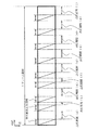
次に、具体例として、各階調におけるサブフレームの選択方法、つまり、各階調において各々のサブフレームを点灯させるのかどうかについて述べる。図 1に、5ビットで階調を表現して、上位ビットを3ビット、下位ビットを2ビットとした場合のサブフレームの選択方法について示す。上位ビットは、重ね合わせ時間階調方式を用いるため、サブフレーム数は7個(SF1〜SF7)である。これにより、3ビットつまり8階調を表現することが出来る。点灯期間(または、ある時間における点灯回数、つまり、重み付けの量)の長さは全て4であるとする。ここで、階調数の1と点灯期間(または、ある時間における点灯回数、つまり、重み付けの量)の長さの1とが対応するものとする。下位ビットは、バイナリコード時間階調方式を用い、サブフレーム数は2個(SF8〜SF9)である。これにより、2ビットつまり4階調を表現することが出来る。点灯期間(または、ある時間における点灯回数、つまり、重み付けの量)の長さはSF8=1、SF9=2であるとする。このように、上位ビットを7個のサブフレーム、下位ビットを2個のサブフレーム、合計サブフレーム数9個で、5ビットの階調を表現することが出来る。
Next, as a specific example, a method for selecting a subframe in each gradation, that is, whether or not each subframe is lit in each gradation will be described. FIG. 1 shows a method for selecting a subframe when gradation is expressed by 5 bits, the upper bit is 3 bits, and the lower bit is 2 bits. Since the upper bits use the superposition time gray scale method, the number of subframes is 7 (SF1 to SF7). Thereby, 3 bits, that is, 8 gradations can be expressed. It is assumed that the length of the lighting period (or the number of times of lighting in a certain time, that is, the weighting amount) is all four. Here, it is assumed that the number of
なお、重ね合わせ時間階調方式を用いる部分のサブフレームにおける点灯期間(または、ある時間における点灯回数、つまり、重み付けの量)の長さは、全て4であるとしたが、これに限定されない。サブフレームによって、点灯期間(または、ある時間における点灯回数、つまり、重み付けの量)の長さが異なっていても良い。 Note that the length of the lighting period (or the number of times of lighting at a certain time, that is, the amount of weighting) in the subframe of the portion using the overlapping time gray scale method is all four, but is not limited thereto. The length of the lighting period (or the number of times of lighting in a certain time, that is, the weighting amount) may be different depending on the subframe.
なお、点灯期間は、ずっと点灯し続ける場合に用いるものであり、点灯回数は、ある時間内において、点滅し続ける場合に用いるものである。点灯回数を用いる代表的なディスプレイは、プラズマディスプレイである。点灯期間を用いる代表的なディスプレイは、有機ELディスプレイである。 The lighting period is used when the lamp continues to be lit, and the lighting count is used when the lamp continues to flash within a certain time. A typical display using the number of times of lighting is a plasma display. A typical display using the lighting period is an organic EL display.
ここで、図1の見方について述べる。丸印がついているサブフレームでは点灯し、ばつ印がついているサブフレームでは非点灯となる。そして、各階調数において、どのサブフレームで点灯するかを選択することにより、階調を表現する。例えば、階調数0では、SF1〜SF9は、非点灯になる。階調数1では、SF1〜SF7、SF9は非点灯となり、SF8は点灯となる。階調数4では、SF2〜SF9は非点灯となり、SF1は点灯となる。階調数5では、SF2〜SF7、SF9は非点灯となり、SF1、SF8は点灯となる。階調数8では、SF3〜SF9は非点灯となり、SF1、SF2は点灯となる。なお、SF1〜SF7は上位ビット用のサブフレームであり、SF8〜SF9は下位ビット用のサブフレームである。
Here, how to view FIG. 1 will be described. Lights up in subframes with a circle mark, and does not light up in subframes with a cross mark. Then, in each gradation number, gradation is expressed by selecting which subframe to light. For example, at the
次に、階調数の表現方法、つまり、各サブフレームの選択方法について述べる。上位ビット3ビット分は、重ね合わせ時間階調方式を用いるため、階調数0〜3までは、SF1〜SF7は全て非点灯となる。階調数4〜7までは、SF1は点灯、SF2〜SF7は全て非点灯となる。階調数8〜11までは、SF1、SF2は点灯、SF3〜SF7は全て非点灯となる。階調数12〜15までは、SF1、SF2、SF3は点灯、SF4〜SF7は全て非点灯となる。さらに階調数が大きくなるときも同様に、点灯、非点灯を選択する。
Next, a method for expressing the number of gradations, that is, a method for selecting each subframe will be described. Since the superimposition time gradation method is used for the upper 3 bits, all of SF1 to SF7 are not lit until the number of
このように、上位3ビットは、各サブフレームにおける点灯期間を順次足し合わせていくことにより、階調を表現する。つまり、階調が大きくなるにしたがって、点灯するサブフレームが増えていくようにする。そのため、SF1は、階調数4以上では全て点灯しており、SF2は、階調数8以上では、全て点灯しており、SF3は、階調数12以上では全て点灯している。SF4〜SF7についても同様である。つまり、小さい階調において点灯しているサブフレームは、大きい階調においても点灯していることになる。 Thus, the upper 3 bits express gradation by sequentially adding the lighting periods in each subframe. That is, the number of subframes to be lit increases as the gray level increases. Therefore, SF1 is all lit when the number of gradations is 4 or more, SF2 is all lit when the number of gradations is 8 or more, and SF3 is all lit when the number of gradations is 12 or more. The same applies to SF4 to SF7. That is, a subframe that is lit at a small gradation is also lit at a large gradation.
このような駆動法にすることにより、疑似輪郭を低減することが出来る。なぜなら、ある階調において、それよりも低い階調において点灯しているサブフレームは、全て点灯しているからである。よって、視線が動いても、階調の変わり目において、不正確な明るさで見えてしまうことを防ぐことが出来る。 By adopting such a driving method, the pseudo contour can be reduced. This is because, in a certain gradation, all subframes that are lit in a gradation lower than that are lit. Therefore, even when the line of sight moves, it can be prevented that the image is viewed with inaccurate brightness at the change of gradation.
次に、下位ビットでの階調の表現方法について述べる。上位ビット分のサブフレームにおいて、点灯するサブフレームが同一の場合は、そのままでは、細かな階調を表現することができない。そこで、より細かな階調を表現するために、つまり、下位ビットを表現するために、バイナリコード時間階調方式を用いる。すなわち、階調数0では、SF8、SF9は非点灯、階調数1では、SF8は点灯、SF9は非点灯、階調数2では、SF8は非点灯、SF9は点灯、階調数3では、SF8、SF9は点灯、となる。同様に、階調数4では、SF8、SF9は非点灯、階調数5では、SF8は点灯、SF9は非点灯、階調数6では、SF8は非点灯、SF9は点灯、階調数7では、SF8、SF9は点灯、となる。
Next, a method of expressing gradation with lower bits will be described. If the subframes to be lit are the same in the subframes for the upper bits, fine gradations cannot be expressed as they are. Therefore, in order to express a finer gradation, that is, to express lower bits, a binary code time gradation method is used. That is, at
このように、サブフレームの長さを1:2:4:8:・・・:2nという感じで、2進法にしたがって、2のべき乗になるようにし、各々のサブフレームの点灯、非点灯を制御して、nビットの階調を表現する。その結果、上位ビット分のサブフレームにおいて、点灯するサブフレームが同一の場合、より細かな階調を表現することが可能となる。すなわち、下位ビットを表現することが可能となる。 In this way, the length of the subframe is 1: 2: 4: 8:...: 2 n , so that it becomes a power of 2 according to the binary system, and each subframe is turned on / off. The lighting is controlled to express an n-bit gradation. As a result, when the subframes to be lit are the same in the subframes for the upper bits, it is possible to express a finer gradation. That is, it is possible to express the lower bits.
このように図1では、上位ビットを3ビット、下位ビットを2ビットとした場合のサブフレームの選択方法について示した。次に、上位ビットを2ビット、下位ビットを3ビットとした場合のサブフレームの選択方法について、図2に示す。 As described above, FIG. 1 shows a subframe selection method when the upper bits are 3 bits and the lower bits are 2 bits. Next, FIG. 2 shows a subframe selection method when the upper bits are 2 bits and the lower bits are 3 bits.
上位2ビットは、重ね合わせ時間階調方式を用いるため、サブフレーム数は3個(SF1〜SF3)である。これにより、2ビットつまり4階調を表現することが出来る。下位3ビットは、バイナリコード時間階調方式を用いるため、サブフレーム数は3個(SF4〜SF6)である。これにより、3ビットつまり8階調を表現することが出来る。このように、上位ビットを3個のサブフレーム、下位ビットを3個のサブフレーム、合計サブフレーム数6個で、5ビットの階調を表現することができる。 Since the upper 2 bits use the superposition time gray scale method, the number of subframes is 3 (SF1 to SF3). Thereby, 2 bits, that is, 4 gradations can be expressed. Since the lower 3 bits use the binary code time gray scale method, the number of subframes is 3 (SF4 to SF6). Thereby, 3 bits, that is, 8 gradations can be expressed. In this way, a 5-bit gray scale can be expressed with three subframes for the upper bits, three subframes for the lower bits, and a total of six subframes.
このように、バイナリコード時間階調方式を用いるビット数を増やすことにより、サブフレーム数のトータル数を減らすことが出来る。しかしそのため、階調数が1つ変わったとき、選択されるサブフレーム、つまり、点灯するサブフレームの選び方が大きく変わってしまう場合がある。そのような時には、疑似輪郭が出やすくなってしまう。したがって、サブフレーム数と疑似輪郭の低減効果とのトレードオフにより、バイナリコード時間階調方式を用いるビット数を決定すればよい。 In this way, the total number of subframes can be reduced by increasing the number of bits using the binary code time gray scale method. However, when the number of gradations changes by one, the selection of the subframe to be selected, that is, the subframe to be lit may change greatly. In such a case, a pseudo contour is likely to appear. Therefore, the number of bits using the binary code time gray scale method may be determined by a trade-off between the number of subframes and the effect of reducing the pseudo contour.
なお、上位ビットを2ビット、下位ビットを3ビットとした場合、重ね合わせ時間階調方式でのサブフレームにおける点灯期間の長さは、8になる。なぜなら、バイナリコード時間階調方式を用いる下位ビットは、3ビット分だからである。3ビット、すなわち、8階調を表現することができるため、重ね合わせ時間階調方式では、点灯期間が最大8づつ増えていく必要がある。以上のことから、重ね合わせ時間階調方式でのサブフレームにおける点灯期間の長さは、バイナリコード時間階調方式における最大階調での点灯期間の長さと等しいか、それ以下にすることが望ましい。重ね合わせ時間階調方式でのサブフレームにおける点灯期間の長さが、バイナリコード時間階調方式における最大階調での点灯期間の長さよりも小さい場合は、バイナリコード時間階調方式において、サブフレームの選び方のうちの幾つかを、実際には用いない、ということになるだけである。 When the upper bit is 2 bits and the lower bit is 3 bits, the length of the lighting period in the subframe in the superposition time gray scale method is 8. This is because the lower bits using the binary code time gray scale method are for 3 bits. Since 3 bits, that is, 8 gradations can be expressed, in the superposition time gradation method, it is necessary to increase the lighting period by 8 at a maximum. From the above, it is desirable that the length of the lighting period in the subframe in the overlapping time gray scale method is equal to or less than the length of the lighting period in the maximum gray scale in the binary code time gray scale method. . If the length of the lighting period in the subframe in the superimposed time gray scale method is smaller than the length of the lighting period in the maximum gray scale in the binary code time gray scale method, the subframe in the binary code time gray scale method It just means that some of the choices are not actually used.
なお、点灯期間の長さは、全体の階調数(ビット数)や全体のサブフレーム数などにより、適宜変わるものである。よって、点灯期間の長さが同じであっても、全体の階調数(ビット数)や全体のサブフレーム数が変われば、実際に点灯している期間の長さ(例えば、何μsであるか)については、変わる可能性がある。 Note that the length of the lighting period varies depending on the total number of gradations (number of bits), the total number of subframes, and the like. Therefore, even if the length of the lighting period is the same, if the total number of gradations (number of bits) or the total number of subframes changes, the length of the actual lighting period (for example, how many μs it is) ) Is subject to change.
次に、6ビットで階調を表現する場合について考える。図3に、上位ビットを3ビット、下位ビットを3ビットとした場合のサブフレームの選択方法について示す。 Next, consider the case of expressing gradation with 6 bits. FIG. 3 shows a subframe selection method when the upper bits are 3 bits and the lower bits are 3 bits.
上位3ビットは、重ね合わせ時間階調方式を用いるため、サブフレーム数は7個(SF1〜SF7)である。これにより、3ビットつまり8階調を表現することが出来る。下位3ビットは、バイナリコード時間階調方式を用いるため、サブフレーム数は3個(SF8〜SF10)である。これにより、3ビットつまり8階調を表現することが出来る。重ね合わせ時間階調方式でのサブフレームにおける点灯期間の長さは、8になる。このように、上位ビットを7個のサブフレーム、下位ビットを3個のサブフレーム、合計サブフレーム数10個で、6ビットの階調を表現することが出来る。 The upper 3 bits use the superposition time gray scale method, so the number of subframes is 7 (SF1 to SF7). Thereby, 3 bits, that is, 8 gradations can be expressed. Since the lower 3 bits use the binary code time gray scale method, the number of subframes is 3 (SF8 to SF10). Thereby, 3 bits, that is, 8 gradations can be expressed. The length of the lighting period in the subframe in the overlapping time gray scale method is 8. In this way, a 6-bit gradation can be expressed by using 7 subframes for the upper bits, 3 subframes for the lower bits, and a total of 10 subframes.
なお、図2と同様、6ビットで階調を表現する場合においても、上位ビットと下位ビットとを任意に分けて、重ね合わせ時間階調方式とバイナリコード時間階調方式とを組み合わせて階調を表現することが可能となる。 As in FIG. 2, even when gradation is expressed by 6 bits, the upper bit and the lower bit are arbitrarily divided, and the combination of the overlapping time gradation method and the binary code time gradation method is used. Can be expressed.
このように、図1〜図3では、5ビットや6ビットの階調を表現する場合について述べてきたが、同様にすることにより、様々なビット数に対応させることが可能となる。つまり、nビットで階調を表現する場合、上位ビットをaビット、下位ビットをbビットとすると、重ね合わせ時間階調方式を用いる上位ビットでは、サブフレーム数は少なくとも(2a −1)個であり、バイナリコード時間階調方式を用いる下位ビットでは、サブフレーム数は少なくともb個となる。重ね合わせ時間階調方式でのサブフレームにおける点灯期間の長さは、2bになる。 As described above, in FIGS. 1 to 3, the case of expressing a gradation of 5 bits or 6 bits has been described. However, by making the same, it is possible to correspond to various numbers of bits. In other words, when the gradation is expressed by n bits, assuming that the upper bit is a bit and the lower bit is b bit, the number of subframes is at least (2 a −1) in the upper bits using the overlapping time gradation method. In the lower bits using the binary code time gray scale method, the number of subframes is at least b. The length of the overlapping lighting period in the subframe in the time gradation method will 2 b.
このように、重ね合わせ時間階調方式とバイナリコード時間階調方式とを組み合わせることにより、サブフレーム数を多くせずに、疑似輪郭を低減したり、階調数を大きくして表示させることが可能となる。 In this way, by combining the overlay time gray scale method and the binary code time gray scale method, the pseudo contour can be reduced or the gray scale number can be displayed without increasing the number of subframes. It becomes possible.
なお、下位ビットを表現するバイナリコード時間階調方式を用いる場合、サブフレームの点灯期間の長さは、一例としては、1:2:4:8:・・・:2nという感じで、2のべき乗になると述べたが、これに限定されない。例えば、バイナリコード時間階調方式を用いる場合における上位ビットのサブフレーム、つまり、期間の長いサブフレームにおいて、サブフレームを分割してもよい。例えば、1:2:(2+2):(3+3+2):・・・という感じにして、長さ4のサブフレームを長さ2のサブフレーム2つに分割したり、長さ8のサブフレームを長さ3と長さ3と長さ2のサブフレーム3つに分割してもよい。図2におけるSF6を二つに分け、SF6、SF7とし、その点灯期間を2に場合について、図4に示す。
In the case of using a binary code time gray scale method for representing lower bits, the length of a lighting period of the subframes, as an example, 1: 2: 4: 8: ...: feeling of 2 n, 2 Although it is said that it becomes the power of, it is not limited to this. For example, subframes may be divided into upper bit subframes in the case of using the binary code time gray scale method, that is, subframes having a long period. For example, a subframe of
ここで、図4に着目すると、バイナリコード時間階調方式を用いている下位ビットのサブフレームにおいて、同じ点灯期間を持つものがあることが分かる。そのような場合、どのサブフレームで点灯させるかを変えることが出来る。例えば、図5に示すように、階調数4,5,10,11,20,21などにおいて、点灯期間の選択の仕方を図4の場合とは異なるようにしてもよい。階調数4の場合、図4では、SF6とSF7で点灯しているが、図5では、SF5とSF7とで点灯している。実際には、同じ点灯期間の中から選択すればよいだけなので、さらに多くの選択の仕方がある。よって、ある階調において、点灯期間の選択の仕方をどれにするかについて、時間的に、または、場所的に変更してもよい。つまり、時刻によって、点灯期間の選択の仕方を変えても良いし、画素によって、点灯期間の選択の仕方を変えても良い。さらに、時刻によって変えて、かつ、画素によっても変えてもよい。
Here, focusing on FIG. 4, it can be seen that there are sub-frames of lower bits using the binary code time gray scale method that have the same lighting period. In such a case, it is possible to change which subframe is lit. For example, as shown in FIG. 5, in the number of
例えば、ある階調を表現するとき、フレーム数が奇数番目のときと、偶数番目のときとで、サブフレームの選択の仕方を変えてもよい。また、ある階調を表現するとき、奇数行目の画素を表示するときと、偶数行目の画素を表示するときとで、サブフレームの選択の仕方を変えてもよい。また、ある階調を表現するとき、奇数列目の画素を表示するときと、偶数列目の画素を表示するときとで、サブフレームの選択の仕方を変えてもよい。 For example, when a certain gradation is expressed, the selection method of subframes may be changed depending on whether the number of frames is an odd number or an even number. In addition, when expressing a certain gradation, the method of selecting a subframe may be changed depending on whether an odd-numbered row pixel is displayed or an even-numbered row pixel is displayed. In addition, when expressing a certain gradation, the method of selecting a subframe may be changed depending on whether an odd-numbered column pixel is displayed or an even-numbered column pixel is displayed.
また、下位ビットを表現するバイナリコード時間階調方式を用いる場合、サブフレームの点灯期間の長さが、2のべき乗にならない場合の別の例を述べる。基本的には、各々のサブフレームを点灯することにより、連続的に階調を表現できればよい。そのためには、あるサブフレームの点灯期間の長さが、それよりも短い点灯期間を持つサブフレームに関して、点灯期間の合計をとったものと同程度であれば、連続的に階調を表現できる。 Another example will be described in which the length of the lighting period of the subframe is not a power of 2 when the binary code time gray scale method expressing the lower bits is used. Basically, it is sufficient that gradations can be expressed continuously by lighting each subframe. For that purpose, if the length of the lighting period of a certain subframe is about the same as the sum of the lighting periods for a subframe having a shorter lighting period, gradation can be expressed continuously. .
例えば、各サブフレームの点灯期間の長さの比が、1:1:2:3とすれば、0から7までの階調を全て連続的に表現できる。つまり、サブフレームiの点灯期間の長さをTiとすると、Tiから点灯期間1を引いたものは、サブフレーム1からサブフレーム(i−1)までの点灯期間の長さの合計と比較して、同じ長さか、それよりも短くなっていればよい。これにより、各サブフレームを適切に選択することにより、階調を全て連続的に表現することが出来る。例えば、T1:T2:T3:T4とした場合、T4から点灯期間1を引いたものは、T1〜T3までの合計以下であればよく、T3から点灯期間1を引いたものは、T1〜T2までの合計以下であればよく、T2から点灯期間1を引いたものは、T1以下であればよい。これにより、階調を全て連続的に表現することが出来る。
For example, if the ratio of the lengths of the lighting periods of the subframes is 1: 1: 2: 3, all the gradations from 0 to 7 can be expressed continuously. That is, if the length of the lighting period of subframe i is Ti, the value obtained by subtracting
このようにして、上位ビットを2ビット、下位ビットを3ビットとした場合のサブフレームの選択方法を図6に示す。下位ビットのサブフレームにおける点灯期間の長さは、1:1:2:3とした。これにより、0から7までの8階調を表現することが出来る。このようにして、図6のようにサブフレームを点灯すると、階調数が変わったときに、選択されているサブフレームの選び方が大きく変わってしまうことを防ぐことができる。そのため、疑似輪郭を低減することが出来る。 FIG. 6 shows a method of selecting a subframe when the upper bits are 2 bits and the lower bits are 3 bits in this way. The length of the lighting period in the sub-frame of the lower bits was 1: 1: 2: 3. Thereby, 8 gradations from 0 to 7 can be expressed. In this way, when the sub-frame is turned on as shown in FIG. 6, it is possible to prevent the method of selecting the selected sub-frame from changing greatly when the number of gradations changes. Therefore, the pseudo contour can be reduced.
ここで、図6に着目すると、バイナリコード時間階調方式を用いている下位ビットに関して、ある階調を表現するときに、サブフレームの選択方法が複数あることが分かる。例えば、階調数2を表現する場合は、点灯期間が1のサブフレームを2つ選択してもよいし、点灯期間が2のサブフレームを1つ選択してもよい。同様に、階調数3を表現する場合は、点灯期間が3のサブフレームを1つ選択してもよいし、点灯期間が1と2のサブフレームを選択してもよい。なお、点灯期間が1のサブフレームは複数ある。よって、どちらを選んでも良い。
Here, paying attention to FIG. 6, it can be seen that there are a plurality of subframe selection methods when a certain gradation is expressed with respect to the lower bits using the binary code time gradation method. For example, when expressing the number of
このように、1つの階調を表現する場合、サブフレームの選択の仕方が複数ある。
よって、ある階調において、サブフレームの選択の仕方をどれにするかについて、時間的に、または、場所的に変更してもよい。つまり、時刻によって、サブフレームの選択の仕方を変えても良いし、画素によって、サブフレームの選択の仕方を変えても良い。さらに、時刻によって変えて、かつ、画素によっても変えてもよい。
As described above, when one gradation is expressed, there are a plurality of methods for selecting a subframe.
Therefore, in a certain gradation, the selection method of subframes may be changed in time or place. That is, the selection method of the subframe may be changed depending on the time, and the selection method of the subframe may be changed depending on the pixel. Further, it may be changed depending on the time and also depending on the pixel.
例えば、ある階調を表現するとき、フレーム数が奇数番目のときと、偶数番目のときとで、サブフレームの選択の仕方を変えてもよい。また、ある階調を表現するとき、奇数行目の画素を表示するときと、偶数行目の画素を表示するときとで、サブフレームの選択の仕方を変えてもよい。また、ある階調を表現するとき、奇数列目の画素を表示するときと、偶数列目の画素を表示するときとで、サブフレームの選択の仕方を変えてもよい。 For example, when a certain gradation is expressed, the selection method of subframes may be changed depending on whether the number of frames is an odd number or an even number. In addition, when expressing a certain gradation, the method of selecting a subframe may be changed depending on whether an odd-numbered row pixel is displayed or an even-numbered row pixel is displayed. In addition, when expressing a certain gradation, the method of selecting a subframe may be changed depending on whether an odd-numbered column pixel is displayed or an even-numbered column pixel is displayed.
なお、これまでは、重ね合わせ時間階調方式とバイナリコード時間階調方式を組み合わせて階調を表現する場合について述べてきたが、さらに別の階調表現方法を組み合わせても良い。例えば、面積階調方式と組み合わせても良い。1つの画素をさらに複数のサブ画素に分割して、点灯している面積を変えることにより、階調を表現する。そのため、疑似輪郭をさらに抑制することが可能となる。 Heretofore, the case where the gradation is expressed by combining the overlay time gradation method and the binary code time gradation method has been described, but another gradation expression method may be combined. For example, it may be combined with an area gradation method. A pixel is further divided into a plurality of sub-pixels, and a gradation is expressed by changing the area that is lit. Therefore, it becomes possible to further suppress the pseudo contour.
これまでは、階調数が増えると、それに線形に比例して点灯期間が増えている場合について述べた。そこで次に、ガンマ補正を行った場合について述べる。ガンマ補正とは、階調数が増えると、非線形で点灯期間が増えていくようにしたものを指す。人間の目は、輝度が線形に比例して大きくなっても、比例して明るくなっているとは感じない。輝度が高くなるほど、明るさの差を感じにくくなっている。よって、人間の目で、明るさの差を感じるようにするためには、階調数が増えていくにしたがって、点灯期間をより長くとる、つまり、ガンマ補正を行う必要がある。 So far, the case where the lighting period increases linearly in proportion to the number of gradations has been described. Next, a case where gamma correction is performed will be described. The gamma correction refers to a non-linear lighting period that increases as the number of gradations increases. Even if the luminance increases linearly in proportion, the human eye does not feel that it is brighter in proportion. The higher the brightness, the less the difference in brightness is felt. Therefore, in order for the human eye to feel a difference in brightness, it is necessary to increase the lighting period as the number of gradations increases, that is, to perform gamma correction.
最も単純な方法は、実際に表示するビット数(階調数)よりも、多くのビット数(階調数)で表示できるようにしておく、というものである。例えば、6ビット(64階調)で表示を行うとき、実際には、8ビット(256階調)を表示できるようにしておく。そして、実際に表示するときには、階調数の輝度が非線形になるようにして、6ビット(64階調)で表示する。これにより、ガンマ補正を実現出来る。 The simplest method is to enable display with a larger number of bits (number of gradations) than the actual number of bits (number of gradations) to be displayed. For example, when displaying with 6 bits (64 gradations), in reality, 8 bits (256 gradations) can be displayed. And when actually displaying, it displays by 6 bits (64 gradations) so that the brightness | luminance of the number of gradations becomes nonlinear. Thereby, gamma correction can be realized.
一例として、6ビットで表示できるようにしておいて、ガンマ補正を行って5ビットで表示する場合のサブフレームの選択方法について、図7に示す。図7では、5ビットでの階調数が12までは、6ビットでの階調数と同じである。しかし、ガンマ補正済みの5ビットでの階調数が13のときは、実際には6ビットの階調数14のサブフレームの選択方法で点灯させる。同様に、ガンマ補正済みの5ビットでの階調数が14のときは、実際には6ビットの階調数16で表示させ、ガンマ補正済みの5ビットでの階調数が15のときは、実際には6ビットの階調数18で表示させる。このように、ガンマ補正済みの5ビットでの階調数と、6ビットでの階調数との対応表を作成し、それに応じて、表示させればよい。これにより、ガンマ補正を実現出来る。 As an example, FIG. 7 shows a method of selecting a subframe in a case where gamma correction is performed so that 6-bit display is possible and display is performed with 5 bits. In FIG. 7, the number of gradations in 5 bits up to 12 is the same as the number of gradations in 6 bits. However, when the number of gray scales with 5 bits after gamma correction is 13, light is actually turned on by a subframe selection method with 14 bits of gray scale levels. Similarly, when the number of gradations with 5 bits after gamma correction is 14, display is actually performed with 16 gradations with 6 bits, and when gradation number with 5 bits after gamma correction is 15, Actually, the display is performed with 18 bits of 6-bit gradation. In this way, a correspondence table between the number of gradations of 5 bits after gamma correction and the number of gradations of 6 bits may be created and displayed accordingly. Thereby, gamma correction can be realized.
なお、ガンマ補正済みの5ビットでの階調数と、6ビットでの階調数との対応表は、適宜変更することが可能である。よって、対応表を変更することにより、ガンマ補正の程度を容易に変更することが可能である。 It should be noted that the correspondence table between the number of gradations of 5 bits after gamma correction and the number of gradations of 6 bits can be changed as appropriate. Therefore, it is possible to easily change the degree of gamma correction by changing the correspondence table.
また、何ビット(例えばpビット、ここでpは整数)を表示できるようにしておいて、ガンマ補正済みで何ビット(例えばqビット、ここでqは整数)で表示するのかについても、これに限定されない。ガンマ補正済みで表示する場合、階調をなめらかに表現するためには、ビット数pを出来るだけ大きくしておくことが望ましい。ただし、あまり大きくしすぎると、サブフレーム数が多くなってしまうなど、弊害も出てきてしまう。よって、ビット数qとビット数pとの関係は、q+2≦p≦q+5、とすることが望ましい。これにより、階調をなめらかに表現しつつ、サブフレーム数も増えすぎない、ということを実現できる。
Also, how many bits (for example, p bits, where p is an integer) can be displayed, and how many bits (for example, q bits, where q is an integer) after gamma correction is displayed. It is not limited. When displaying with gamma correction, it is desirable to increase the number of bits p as much as possible in order to express gradation smoothly. However, if it is made too large, there will be adverse effects such as an increase in the number of subframes. Therefore, it is desirable that the relationship between the number of bits q and the number of bits p is q + 2 ≦ p ≦
別のガンマ補正の方法としては、上位ビットにおいて、重ね合わせ時間階調方式を用いる場合、そのサブフレームにおける点灯期間の長さが異なるようにするというものである。 As another gamma correction method, when the superposition time gray scale method is used in the upper bits, the lengths of the lighting periods in the subframes are made different.
例として、階調数0から15までは、通常通りで、階調数16から31までは、階調数に対する点灯期間の変化量を2倍にした場合のサブフレームの選択方法を図8に示す。この場合、図1と比較すると、上位ビット向けである重ね合わせ時間階調方式で用いるサブフレームの中で、より上位のビットのサブフレームに対応するサブフレーム5(SF5)〜サブフレーム7(SF7)までの各々の点灯期間が2倍になっていることと、バイナリコード時間階調方式を用いる下位ビット向けとして、サブフレームが追加になっていることとが異なる。
As an example, FIG. 8 shows a subframe selection method in which the number of
階調数0から15までは、バイナリコード時間階調方式を用いるサブフレームは、SF8とSF9である。一方、階調数16から31までは、バイナリコード時間階調方式を用いるサブフレームは、SF9とSF10である。このようにすることにより、階調が大きくなっていくにしたがって、なめらかに点灯期間も変化していくようになる。
For the
このようにすることにより、疑似輪郭を低減することが可能となる。 By doing so, the pseudo contour can be reduced.
なお、図8では、重ね合わせ時間階調方式で用いるサブフレームにおける点灯期間の長さを2倍で異なるようにしたが、これに限定されない。ガンマ補正を行うときのガンマ値によって、調整すればよい。つまり、重ね合わせ時間階調方式で用いるサブフレームにおける点灯期間の長さが、異なっていて、より長くなるようになっていればよい。 In FIG. 8, the length of the lighting period in the subframe used in the overlapping time gray scale method is set to be twice different, but the present invention is not limited to this. Adjustment may be made according to the gamma value when performing gamma correction. That is, the length of the lighting period in the subframe used in the overlapping time gray scale method is different as long as it is longer.
なお、図8では、階調の領域を2つにわけていたが、これに限定されない。もっと多くの領域に分けてもよい。一例として、4つに分けた場合を図9に示す。 In FIG. 8, the gradation area is divided into two, but the present invention is not limited to this. It may be divided into more areas. As an example, FIG. 9 shows a case where it is divided into four.
まず、領域を階調数0から7までと、8から15までと、16から23までと、24から31までに分ける。そして、階調数0から7までは通常通りで、階調数8から15までは、階調数に対する点灯期間の変化量が2倍になっており、階調数16から23までは、階調数に対する点灯期間の変化量がさらに2倍になっており、階調数24から31までは、階調数に対する点灯期間の変化量がさらに2倍になっている。この場合、上位ビット向けである重ね合わせ時間階調方式で用いるサブフレームの中で、より上位のビットのサブフレームになるほど、点灯期間が2倍ずつ長くなっている。また、バイナリコード時間階調方式を用いる下位ビット向けとして、サブフレーム数がさらに多くなっている。
First, the area is divided into
階調数0から7までは、バイナリコード時間階調方式を用いるサブフレームは、SF8とSF9であり、階調数8から15までは、バイナリコード時間階調方式を用いるサブフレームは、SF9とSF10であり、階調数16から23までは、バイナリコード時間階調方式を用いるサブフレームは、SF10とSF11であり、階調数24から31までは、バイナリコード時間階調方式を用いるサブフレームは、SF11とSF12である。このようにすることにより、階調が大きくなっていくにしたがって、なめらかに点灯期間も変化していくようになる。
For
なお、階調の領域ごとに、階調数に対する点灯期間の長さが2倍ずつ大きくなっているが、これに限定されない。4倍ずつや8倍ずつなど、2のべき乗ずつ大きくなっていってもよい。あるいは、少しずつ大きくなっていってもよい。ガンマ補正を行うときのガンマ値によって、調整すればよい。つまり、重ね合わせ時間階調方式で用いるサブフレームにおける点灯期間の長さが、異なっていて、より長くなるようになっていればよい。 Note that although the length of the lighting period with respect to the number of gradations is doubled for each gradation region, the present invention is not limited to this. It may be increased by a power of 2, such as 4 times or 8 times. Or you may become large little by little. Adjustment may be made according to the gamma value when performing gamma correction. That is, the length of the lighting period in the subframe used in the overlapping time gray scale method is different as long as it is longer.
ここまでは、階調の表現方法、つまり、サブフレームの選択方法について述べた。次に、サブフレームの出現順序について述べる。 So far, the gradation expression method, that is, the subframe selection method has been described. Next, the appearance order of subframes will be described.
ここでは、例として、図1の場合を用いるが、これに限定されず、他の図に対しても同様に適用できる。 Here, the case of FIG. 1 is used as an example, but the present invention is not limited to this, and can be similarly applied to other drawings.
まず、最も基本的なものは、SF8、SF9、SF1、SF2、SF3、SF4、SF5、SF6、SF7という順序で1フレームが構成される、というものである。最も点灯期間が短いものから、サブフレームが始まり、その後は、重ね合わせ時間階調方式において、点灯していくサブフレームが順序よくならんでいく、というものである。 First, the most basic one is that one frame is configured in the order of SF8, SF9, SF1, SF2, SF3, SF4, SF5, SF6, and SF7. The sub-frame starts from the shortest lighting period, and thereafter, the sub-frames that are lit up are arranged in order in the overlapping time gray scale method.
または、逆の順序として、SF7、SF6、SF5、SF4、SF3、SF2、SF1、SF9、SF8でもよい。また、バイナリコード時間階調方式と重ね合わせ時間階調方式が出現する順序が逆でもよい。例えば、SF1、SF2、SF3、SF4、SF5、SF6、SF7、SF8、SF9でもよい。 Alternatively, the reverse order may be SF7, SF6, SF5, SF4, SF3, SF2, SF1, SF9, SF8. The order in which the binary code time gray scale method and the overlay time gray scale method appear may be reversed. For example, SF1, SF2, SF3, SF4, SF5, SF6, SF7, SF8, and SF9 may be used.
次は、重ね合わせ時間階調方式でのサブフレームの間のどこかに、バイナリコード時間階調方式でのサブフレームが挿入されている、というものである。例えば、SF1、SF8、SF2、SF9、SF3、SF4、SF5、SF6、SF7という感じで、バイナリコード時間階調方式でのサブフレームSF8、SF9が、重ね合わせ時間階調方式でのサブフレームであるSF1とSF2の間、SF2とSF3の間に挿入されている。なお、バイナリコード時間階調方式でのサブフレームを挿入する場所は、これに限定されない。また、挿入するサブフレーム数も、これに限定されない。 Next, a subframe in the binary code time gray scale method is inserted somewhere between the subframes in the superposition time gray scale method. For example, SF1, SF8, SF2, SF9, SF3, SF4, SF5, SF6, and SF7, subframes SF8 and SF9 in the binary code time gray scale method are subframes in the superposed time gray scale method. It is inserted between SF1 and SF2 and between SF2 and SF3. Note that the place where the subframe is inserted in the binary code time gray scale method is not limited to this. Further, the number of subframes to be inserted is not limited to this.
このように、バイナリコード時間階調方式でのサブフレームを重ね合わせ時間階調方式でのサブフレームの順序の中に挿入することにより、目が誤魔化されるため、疑似輪郭がより見えにくくなる。 In this way, by inserting subframes in the binary code time gray scale method into the subframe order in the superposition time gray scale method, the eyes are deceived so that the pseudo contour becomes less visible.
そこで、5ビットの場合で、SF1、SF8、SF2、SF3、SF4、SF5、SF9、SF6、SF7という順序で並べた場合について、図10に示す。画素Aでは、階調数15を表示し、画素Bでは、階調数16で表示しているとする。ここで、視線がうごいたとすると、視線の追い方によって、あるときは階調数が17(=4+1+4+4+4)と感じ、また別のあるときは、階調数が14(=4+4+4+2)と感じてしまう。本来は、階調数が15と16に見えるべきであるが、階調数が16から17くらいで見えている。よって、階調のずれが非常に小さいため、疑似輪郭が低減されている。
Therefore, FIG. 10 shows a case of 5 bits arranged in the order of SF1, SF8, SF2, SF3, SF4, SF5, SF9, SF6, and SF7. It is assumed that the pixel A displays the
なお、重ね合わせ時間階調方式におけるサブフレームは、点灯していく順に並んでいてもよいし(例えば、SF1、SF2、SF3、SF4、SF5、SF6、SF7)、その逆順でもよい(例えば、SF7、SF6、SF5、SF4、SF3、SF2、SF1)。あるいは、真ん中から徐々に点灯していくようにしてもよい(SF7、SF5、SF5、SF3、SF2、SF4、SF6)。このようにすることにより、1フレーム目から2フレーム目に変わるときに、切り替わり目で疑似輪郭が出てしまうことを少なくすることが出来る。いわゆる、動画疑似輪郭を低減することが可能となる。 Note that the subframes in the overlapping time gray scale method may be arranged in the order of lighting (for example, SF1, SF2, SF3, SF4, SF5, SF6, SF7), or the reverse order (for example, SF7). , SF6, SF5, SF4, SF3, SF2, SF1). Or you may make it light up gradually from the middle (SF7, SF5, SF5, SF3, SF2, SF4, SF6). By doing in this way, when changing from the first frame to the second frame, it is possible to reduce the occurrence of a pseudo contour at the switching point. So-called moving image pseudo contour can be reduced.
あるいは、全くランダムな順序に並んでいてもよい(例えば、SF1、SF6、SF2、SF4、SF3、SF5、SF7)。このようにすることにより、目が誤魔化されやすくなるため、疑似輪郭がより見えにくくなる。 Alternatively, they may be arranged in a completely random order (for example, SF1, SF6, SF2, SF4, SF3, SF5, SF7). By doing so, the eyes are easily deceived, so that the pseudo contour is less visible.
例として、1フレーム全体のサブフレームの出現順序が、SF1、SF8、SF5、SF7、SF2、SF4、SF9、SF3、SF6、というように並んでいるとする。これは、重ね合わせ時間階調方式におけるサブフレームがランダムな順にならんでおり、バイナリコード時間階調方式でのサブフレームが、重ね合わせ時間階調方式におけるサブフレームの間に配置されているものに相当する。 As an example, it is assumed that the appearance order of the subframes of one entire frame is arranged as follows: SF1, SF8, SF5, SF7, SF2, SF4, SF9, SF3, SF6. This is because the subframes in the superposition time gray scale method are arranged in a random order, and the subframes in the binary code time gray scale method are arranged between the subframes in the superposition time gray scale method. Equivalent to.
その場合を、図 11に示す。ここで、視線がうごいたとすると、視線の追い方によって、あるときは階調数が17(=4+1+4+4+4)と感じ、また別のあるときは、階調数が14(=4+4+2+4)と感じてしまう。本来は、階調数が15と16に見えるべきであるが、階調数が16から17くらいで見えている。よって、図10の場合と、図11の場合とでは、大差ない。 This case is shown in FIG. Here, if the line of sight is moving, depending on how the line of sight is followed, the number of gradations may be 17 (= 4 + 1 + 4 + 4 + 4) in some cases, and the gradation number may be 14 (= 4 + 4 + 2 + 4) in other cases. . Originally, the number of gradations should be visible as 15 and 16, but the number of gradations is visible between 16 and 17. Therefore, there is no great difference between the case of FIG. 10 and the case of FIG.
しかし、視線が急激に動いたとする。例えば、図10の場合において、視線が急激に動いた場合を図12に示す。視線が急激にうごいたとすると、視線の追い方によって、あるときは階調数が12(=4+4+4)と感じ、また別のあるときは、階調数が19(=4+1+4+4+4+2)と感じてしまう。本来は、階調数が15と16に見えるべきであるが、階調数が12から19くらいで見えてしまう。
However, suppose that the line of sight moves suddenly. For example, FIG. 12 shows a case where the line of sight moves suddenly in the case of FIG. If the line of sight suddenly moves, depending on how the line of sight is followed, the number of gradations may be felt 12 (= 4 + 4 + 4) in some cases, and the
一方、図11の場合において、視線が急激に動いた場合を図13に示す。視線が急激にうごいたとすると、視線の追い方によって、あるときは階調数が16(=4+4+4+4)と感じ、また別のあるときは、階調数が15(=4+1+4+2+4)と感じてしまう。本来は、階調数が15と16に見えるべきであるので、おおよそ正しく見えている。よって、図12の場合と、図13の場合とでは、大きく異なる。つまり、重ね合わせ時間階調方式におけるサブフレームにおいても、出来るだけランダムに配置した方が、疑似輪郭を低減する効果は高くなる。 On the other hand, FIG. 13 shows a case where the line of sight moves rapidly in the case of FIG. If the line of sight rapidly moves, depending on how the line of sight is followed, the number of gradations may be 16 (= 4 + 4 + 4 + 4) in some cases, and the gradation number may be 15 (= 4 + 1 + 4 + 2 + 4) in other cases. Originally, since the number of gradations should be 15 and 16, it looks roughly correct. Therefore, the case of FIG. 12 and the case of FIG. 13 are greatly different. That is, even in the subframes in the superposition time gray scale method, the effect of reducing the pseudo contour is enhanced by arranging them as randomly as possible.
このように、重ね合わせ時間階調方式におけるサブフレームの順序を決定し、そのサブフレームの間に、バイナリコード時間階調方式でのサブフレームを挿入する形で、全体のサブフレームの出現順序を決めればよい。 In this way, the order of subframes in the overlapped time gray scale method is determined, and the subframes in the binary code time gray scale method are inserted between the subframes, so that the appearance order of the entire subframe is determined. Just decide.
このとき、バイナリコード時間階調方式は、点灯期間が短い順に並んでも良いし(例えば、SF8、SF9)、その逆順でもよい(例えば、SF9、SF8)。あるいは、真ん中から徐々に点灯していくようにしてもよい。あるいは、全くランダムな順序に並んでいてもよい。このようにすることにより、目が誤魔化されやすくなるため、疑似輪郭がより見えにくくなる。 At this time, the binary code time gray scale method may be arranged in the order of short lighting periods (for example, SF8, SF9), or vice versa (for example, SF9, SF8). Or you may make it light up gradually from the center. Alternatively, they may be arranged in a completely random order. By doing so, the eyes are easily deceived, so that the pseudo contour is less visible.
また、重ね合わせ時間階調方式におけるサブフレームの間に、バイナリコード時間階調方式でのサブフレームを挿入する場合、そのサブフレーム数に限定はない。 In addition, when a subframe in the binary code time gray scale method is inserted between subframes in the overlapping time gray scale method, the number of subframes is not limited.
また、このように、バイナリコード時間階調方式におけるサブフレームの順序を決定し、そのサブフレームの間に、重ね合わせ時間階調方式でのサブフレームを挿入する形で、全体のサブフレームの出現順序を決めてもよい。 In addition, in this way, the order of the subframes in the binary code time gray scale method is determined, and the subframes in the superimposed time gray scale method are inserted between the subframes so that the entire subframe appears. The order may be determined.
このように、重ね合わせ時間階調方式におけるサブフレームの間に、バイナリコード時間階調方式におけるサブフレームを配置して、サブフレームが偏在しないようにする。その結果、目が誤魔化されて、疑似輪郭を低減出来る。 In this way, subframes in the binary code time gray scale method are arranged between subframes in the overlapping time gray scale method so that the subframes are not unevenly distributed. As a result, the eyes are deceived and pseudo contours can be reduced.
例として、図3の場合について、サブフレームの出現順序のパターン例を図14に示す。 As an example, FIG. 14 shows a pattern example of the appearance order of subframes in the case of FIG.
1つ目のパターンとしては、SF1、SF2、SF3、SF4、SF5、SF6、SF7、SF8、SF9、SF10、というものである。バイナリコード時間階調方式におけるサブフレームが、最後にまとまって配置されている。 The first pattern is SF1, SF2, SF3, SF4, SF5, SF6, SF7, SF8, SF9, SF10. Subframes in the binary code time gray scale method are arranged together at the end.
2つ目のパターンとしては、SF8、SF9、SF10、SF1、SF2、SF3、SF4、SF5、SF6、SF7、というものである。バイナリコード時間階調方式におけるサブフレームが、最初にまとまって配置されている。 The second pattern is SF8, SF9, SF10, SF1, SF2, SF3, SF4, SF5, SF6, SF7. The subframes in the binary code time gray scale method are arranged together first.
3つ目のパターンとしては、SF1、SF2、SF3、SF4、SF8、SF9、SF10、SF6、SF7、SF5、というものである。バイナリコード時間階調方式におけるサブフレームが、真ん中にまとまって配置されている。 The third pattern is SF1, SF2, SF3, SF4, SF8, SF9, SF10, SF6, SF7, SF5. Subframes in the binary code time gray scale method are arranged together in the middle.
4つ目のパターンとしては、SF1、SF2、SF8、SF3、SF4、SF9、SF5、SF6、SF10、SF8というものである。重ね合わせ時間階調方式におけるサブフレームは、順序よく並んでいる。バイナリコード時間階調方式におけるサブフレームも、順序よく並んでいる。そして、重ね合わせ時間階調方式におけるサブフレームが2つ並んだ後、バイナリコード時間階調方式におけるサブフレームが1つ配置されている。 The fourth pattern is SF1, SF2, SF8, SF3, SF4, SF9, SF5, SF6, SF10, SF8. The subframes in the overlapping time gray scale method are arranged in order. The subframes in the binary code time gray scale method are also arranged in order. Then, after two subframes in the overlapping time gray scale method are arranged, one subframe in the binary code time gray scale method is arranged.
5つ目のパターンとしては、SF1、SF2、SF9、SF3、SF4、SF8、SF5、SF6、SF10、SF8というものである。これは、4つ目のパターンに対して、バイナリコード時間階調方式におけるサブフレームの出現順序をランダムにしたものである。 The fifth pattern is SF1, SF2, SF9, SF3, SF4, SF8, SF5, SF6, SF10, SF8. This is a randomized subframe appearance order in the binary code time gray scale method for the fourth pattern.
6つ目のパターンとしては、SF1、SF5、SF8、SF2、SF7、SF9、SF3、SF6、SF10、SF4というものである。これは、4つ目のパターンに対して、重ね合わせ時間階調方式におけるサブフレームの出現順序をランダムにしたものである。 The sixth pattern is SF1, SF5, SF8, SF2, SF7, SF9, SF3, SF6, SF10, SF4. In this case, the appearance order of the subframes in the overlapping time gray scale method is made random with respect to the fourth pattern.
7つ目のパターンとしては、SF1、SF5、SF9、SF2、SF7、SF8、SF3、SF6、SF10、SF4というものである。これは、4つ目のパターンに対して、重ね合わせ時間階調方式におけるサブフレームの出現順序と、バイナリコード時間階調方式におけるサブフレームの出現順序とをランダムにしたものである。 The seventh pattern is SF1, SF5, SF9, SF2, SF7, SF8, SF3, SF6, SF10, SF4. This is a random pattern of the subframe appearance order in the overlapping time gray scale method and the subframe appearance order in the binary code time gray scale method for the fourth pattern.
8つ目のパターンとしては、SF1、SF2、SF8、SF3、SF9、SF4、SF5、SF6、SF10、SF8というものである。これは、重ね合わせ時間階調方式におけるサブフレームが2つ並んだ後、バイナリコード時間階調方式におけるサブフレームが1つ配置され、重ね合わせ時間階調方式におけるサブフレームが1つ配置され、バイナリコード時間階調方式におけるサブフレームが1つ配置され、重ね合わせ時間階調方式におけるサブフレームが3つ配置され、バイナリコード時間階調方式におけるサブフレームが1つ配置されたものである。 The eighth pattern is SF1, SF2, SF8, SF3, SF9, SF4, SF5, SF6, SF10, SF8. This is because, after two subframes in the superimposition time gray scale method are arranged, one subframe in the binary code time gray scale method is arranged, and one subframe in the superposition time gray scale method is arranged. One subframe in the code time gray scale method is arranged, three subframes in the superposition time gray scale method are arranged, and one subframe in the binary code time gray scale method is arranged.
9つ目のパターンとしては、SF1、SF2、SF3、SF4、SF8、SF9、SF5、SF6、SF7、SF10というものである。これは、重ね合わせ時間階調方式におけるサブフレームが4つ並んだ後、バイナリコード時間階調方式におけるサブフレームが2つ配置され、重ね合わせ時間階調方式におけるサブフレームが3つ配置され、バイナリコード時間階調方式におけるサブフレームが1つ配置されたものである。 The ninth pattern is SF1, SF2, SF3, SF4, SF8, SF9, SF5, SF6, SF7, SF10. This is because, after four subframes in the superposition time gray scale method are arranged, two subframes in the binary code time gray scale method are arranged, and three subframes in the superposition time gray scale method are arranged. One subframe in the code time gray scale method is arranged.
このように、上位のビットに相当する複数のサブフレームのうちの一つのサブフレームが点灯し、その後、下位のビットに相当する一つ以上のサブフレームのうちの一つのサブフレームが点灯し、その後、上位のビットに相当する複数のサブフレームのうちの別の一つのサブフレームが点灯する、とすることが望ましい。 In this way, one subframe of a plurality of subframes corresponding to the upper bits is lit, and then one subframe of one or more subframes corresponding to the lower bits is lit. Thereafter, it is desirable that another one of the plurality of subframes corresponding to the upper bits is turned on.
また、下位のビットに相当する複数のサブフレームのうちの一つのサブフレームが点灯し、その後、上位のビットに相当する複数のサブフレームのうちの一つのサブフレームが点灯し、その後、下位のビットに相当する複数のサブフレームのうちの別の一つのサブフレームが点灯する、とすることが望ましい。 Also, one subframe of a plurality of subframes corresponding to the lower bits is lit, and then one subframe of the plurality of subframes corresponding to the upper bits is lit, and then the lower It is desirable that another one of the plurality of subframes corresponding to the bits is turned on.
また、下位のビットに相当する複数のサブフレームのうちの一つのサブフレームが点灯し、その後、上位のビットに相当する複数のサブフレームのうちの複数のサブフレームが点灯し、その後、前記下位のビットに相当する複数のサブフレームのうちの別の一つのサブフレームが点灯する、とすることが望ましい。 Also, one subframe of a plurality of subframes corresponding to the lower bits is lit, and then a plurality of subframes of the plurality of subframes corresponding to the upper bits are lit, and then the lower order It is desirable that another one of the plurality of subframes corresponding to the bits of the above is turned on.
また、上位のビットに相当する複数のサブフレームのうちの一つのサブフレームが点灯し、その後、下位のビットに相当する複数のサブフレームのうちの複数のサブフレームが点灯し、その後、上位のビットに相当する複数のサブフレームのうちの別の一つのサブフレームが点灯する、とすることが望ましい。 Also, one subframe of a plurality of subframes corresponding to the upper bits is lit, and then a plurality of subframes of the plurality of subframes corresponding to the lower bits are lit, and then the upper bits It is desirable that another one of the plurality of subframes corresponding to the bits is turned on.
次に、図4の場合のサブフレームの出現順序について述べる。図4の場合、バイナリコード時間階調方式における上位のサブフレームを分割している。よって、サブフレームの出現順序も、それに見合ったものにする必要がある。例としては、SF4、SF1、SF6、SF2、SF5、SF3、SF7という感じである。このように、重ね合わせ時間階調方式におけるサブフレームの間に、バイナリコード時間階調方式におけるサブフレームを配置し、かつ、バイナリコード時間階調方式におけるサブフレームは、上位ビットのサブフレームを出来るだけ離れて配置するようにする。その結果、疑似輪郭を低減することが出来る。 Next, the subframe appearance order in the case of FIG. 4 will be described. In the case of FIG. 4, the upper subframe in the binary code time gray scale method is divided. Therefore, it is necessary to make the appearance order of the subframes suitable for it. For example, the feeling is SF4, SF1, SF6, SF2, SF5, SF3, SF7. In this way, subframes in the binary code time gray scale method are arranged between subframes in the superposition time gray scale method, and the subframe in the binary code time gray scale method can be a subframe of higher bits. Just try to place them apart. As a result, the pseudo contour can be reduced.
なお、重ね合わせ時間階調方式におけるサブフレームの順序も、図1の場合と同様、点灯していく順やその逆、もしくは、ランダムな順序で並べればよい。バイナリコード時間階調方式におけるサブフレームを、重ね合わせ時間階調方式におけるサブフレームの中にどのような順序で挿入するかは、サブフレームが偏在しないようにして、適宜決定すればよい。その結果、疑似輪郭を低減出来る。 Note that the order of the subframes in the overlapping time gray scale method may be arranged in the order of lighting, the reverse thereof, or the random order as in the case of FIG. The order in which the subframes in the binary code time gray scale method are inserted into the subframes in the superposition time gray scale method may be determined as appropriate so that the subframes are not unevenly distributed. As a result, the pseudo contour can be reduced.
なお、サブフレームの出現順序は、時刻によって変化してもよい。例えば、1フレーム目と2フレーム目とで、サブフレームの出現順序が変わっても良い。また、サブフレームの出現順序は、場所によって変わっても良い。例えば、画素Aと画素Bとで、サブフレームの出現順序が変わっても良い。また、それらを組み合わせて、サブフレームの出現順序が、時刻によって変化して、かつ、場所によって変化してもよい。 Note that the appearance order of the subframes may change depending on the time. For example, the appearance order of subframes may change between the first frame and the second frame. Further, the appearance order of subframes may vary depending on the location. For example, the appearance order of the subframes may be changed between the pixel A and the pixel B. In addition, by combining them, the appearance order of the subframes may change with time and change with place.
なお、通常のフレーム周波数は、60ヘルツであるが、これに限定されない。フレーム周波数をもっと上げることにより、疑似輪郭を低減してもよい。例えば、通常の倍の周波数120ヘルツ程度で動作させてもよい。 The normal frame frequency is 60 Hz, but is not limited to this. The pseudo contour may be reduced by further increasing the frame frequency. For example, the operation may be performed at a frequency that is about twice that of a normal frequency of 120 Hz.
(実施の形態2)
本実施の形態では、タイミングチャートの例について述べる。サブフレームの選択方法は、一例として、図1のものを用いることにするが、これに限定されず、他のサブフレームの選択方法や他の階調数などにも容易に適用可能である。
(Embodiment 2)
In this embodiment, an example of a timing chart is described. As an example, the subframe selection method shown in FIG. 1 is used. However, the subframe selection method is not limited to this, and the method can be easily applied to other subframe selection methods and other gradation numbers.
また、サブフレームが出現する順番は、一例として、SF1、SF8、SF2、SF9、SF3、SF4、SF5、SF6、SF7であるとするが、これに限定されず、他の順番にも容易に適用可能である。 In addition, the order in which subframes appear is, for example, SF1, SF8, SF2, SF9, SF3, SF4, SF5, SF6, and SF7, but is not limited to this, and can be easily applied to other orders. Is possible.
まず、画素に信号を書き込む期間と点灯する期間とが分離されている場合のタイミングチャートを図15に示す。まず、信号書き込み期間において、1画面分の信号を全画素に入力する。この間は、画素は点灯しない。信号書き込み期間が終了したのち、点灯期間が始まり、画素が点灯する。そのときの点灯期間の長さは、4である。次に、次のサブフレームが始まり、信号書き込み期間において、1画面分の信号を全画素に入力する。この間は、画素は点灯しない。信号書き込み期間が終了したのち、点灯期間が始まり、画素が点灯する。そのときの点灯期間の長さは、1である。 First, FIG. 15 shows a timing chart in the case where a period for writing a signal to a pixel and a lighting period are separated. First, in a signal writing period, a signal for one screen is input to all pixels. During this time, the pixels are not lit. After the signal writing period ends, the lighting period starts and the pixels are lit. The length of the lighting period at that time is 4. Next, the next subframe starts, and a signal for one screen is input to all pixels in the signal writing period. During this time, the pixels are not lit. After the signal writing period ends, the lighting period starts and the pixels are lit. The length of the lighting period at that time is 1.
同様のことを繰り返すことにより、点灯期間の長さが、4、1、4、2、4、4、4、4、4という順序で配置される。 By repeating the same, the lengths of the lighting periods are arranged in the order of 4, 1, 4, 2, 4, 4, 4, 4, 4.
このように、画素に信号を書き込む期間と点灯する期間とが分離されている駆動方法は、プラズマディスプレイに適用することが好適である。なお、プラズマディスプレイに用いる場合は、初期化の動作などが必要になる。しかしながら、簡単のため、省略している。 As described above, the driving method in which the signal writing period and the lighting period are separated from each other is preferably applied to the plasma display. In the case of using for a plasma display, an initialization operation or the like is required. However, it is omitted for simplicity.
また、この駆動方法は、有機ELディスプレイやフィールドエミッションディスプレイやデジタル・マイクロミラー・デバイス(DMD)を用いたディスプレイなどに適用することも好適である。 This driving method is also preferably applied to an organic EL display, a field emission display, a display using a digital micromirror device (DMD), and the like.
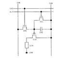
その場合の画素構成を図16に示す。ゲート線1607を選択して、選択トランジスタ1601をオン状態にして、信号線1605から信号を保持容量1602に入力する。すると、その信号に応じて、駆動トランジスタ1603の電流が制御され、第1電源線1606から、表示素子1604を通って、第2電源線1608に電流が流れる。
FIG. 16 shows a pixel configuration in that case. The
なお、信号書き込み期間においては、第1電源線1606と第2電源線1608の電位を制御することにより、表示素子1604には電圧が加わらないようにしておく。その結果、信号書き込み期間において、表示素子1604が点灯することを避けることが出来る。
Note that in the signal writing period, the potential of the first
次に、画素に信号を書き込む期間と点灯する期間とが分離されていない場合のタイミングチャートを図17に示す。各行において、信号書き込み動作を行うと、すぐに点灯期間が開始する。 Next, FIG. 17 shows a timing chart in the case where the period for writing a signal to the pixel and the lighting period are not separated. When a signal writing operation is performed in each row, the lighting period starts immediately.
ある行において、信号を書き込み、所定の点灯期間が終了したのち、次のサブフレームにおける信号の書き込み動作を開始する。これを繰り返すことにより、点灯期間の長さが、4、1、4、2、4、4、4、4、4という順序で配置される。 In a certain row, a signal is written, and after a predetermined lighting period ends, a signal writing operation in the next subframe is started. By repeating this, the length of the lighting period is arranged in the order of 4, 1, 4, 2, 4, 4, 4, 4, 4.
このようにすることにより、信号の書き込み動作が遅くても、1フレーム内にたくさんのサブフレームを配置することが可能となる。 This makes it possible to arrange many subframes in one frame even if the signal writing operation is slow.
このような駆動方法は、プラズマディスプレイに適用することが好適である。なお、プラズマディスプレイに用いる場合は、初期化の動作などが必要になるが、簡単のため初期化の動作を省略している。 Such a driving method is preferably applied to a plasma display. In the case of use in a plasma display, an initialization operation is required, but the initialization operation is omitted for simplicity.
また、この駆動方法は、有機ELディスプレイやフィールドエミッションディスプレイやデジタル・マイクロミラー・デバイス(DMD)を用いたディスプレイなどに適用することも好適である。 This driving method is also preferably applied to an organic EL display, a field emission display, a display using a digital micromirror device (DMD), and the like.
その場合の画素構成を図18に示す。第1ゲート線1807を選択して、第1選択トランジスタ1801をオン状態にして、第1信号線1805から信号を保持容量1802に入力する。すると、その信号に応じて、駆動トランジスタ1803の電流が制御され、第1電源線1806から、表示素子1804を通って、第2電源線1808に電流が流れる。同様に、第2ゲート線1817を選択して、第2選択トランジスタ1811をオン状態にして、第2信号線1815から信号を保持容量1802に入力する。すると、その信号に応じて、駆動トランジスタ1803の電流が制御され、第1電源線1806から、表示素子1804を通って、第2電源線1808に電流が流れる。
The pixel configuration in that case is shown in FIG. The
第1ゲート線1807と第2ゲート線1817とは、別々に制御出来る。同様に、第1信号線1805と第2信号線1815とは、別々に制御出来る。よって、同時に2行分の画素に信号を入力することが可能であるため、図17のような駆動法が実現出来る。
The
なお、図16の回路を用いて、図17のような駆動法を実現することも可能である。その場合のタイミングチャートを図19に示す。図19に示すように、1ゲート選択期間を複数(図19では2つ)に分割する。そして、分割された選択期間内で、各々のゲート線を選択し、その時に対応する信号を第1信号線1805に入力する。例えば、ある1ゲート選択期間において、前半はi行目を選択し、後半はj行目を選択する。すると、1ゲート選択期間において、あたかも同時に2行分を選択したかのように動作させることが可能となる。
Note that the driving method shown in FIG. 17 can be realized by using the circuit shown in FIG. FIG. 19 shows a timing chart in that case. As shown in FIG. 19, one gate selection period is divided into a plurality (two in FIG. 19). Then, each gate line is selected within the divided selection period, and a corresponding signal is input to the
なお、このような駆動方法の詳細については、例えば、特開2001−324958号公報等に記載されており、その内容を本願と組み合わせて適用することが出来る。 Details of such a driving method are described in, for example, Japanese Patent Application Laid-Open No. 2001-324958, and the contents thereof can be applied in combination with the present application.
次に、画素の信号を消去する動作を行う場合のタイミングチャートを図20に示す。各行において、信号書き込み動作を行い、次の信号書き込み動作が来る前に、画素の信号を消去する。このようにすることにより、点灯期間の長さを容易に制御できるようになる。 Next, FIG. 20 shows a timing chart in the case of performing an operation of erasing the pixel signal. In each row, a signal writing operation is performed, and the pixel signal is erased before the next signal writing operation is performed. In this way, the length of the lighting period can be easily controlled.
ある行において、信号を書き込み、所定の点灯期間が終了したのち、次のサブフレームにおける信号の書き込み動作を開始する。もし、点灯期間が短い場合は、信号消去動作を行い、非点灯状態にする。このような動作を繰り返すことにより、点灯期間の長さが、4、1、4、2、4、4、4、4、4という順序で配置される。 In a certain row, a signal is written, and after a predetermined lighting period ends, a signal writing operation in the next subframe is started. If the lighting period is short, a signal erasing operation is performed to turn off the light. By repeating such an operation, the lighting periods are arranged in the order of 4, 1, 4, 2, 4, 4, 4, 4, 4.
なお、図20では、点灯期間が1と2の場合において、信号消去動作を行っているが、これに限定されない。他の点灯期間においても、消去動作を行っても良い。 In FIG. 20, the signal erasing operation is performed when the lighting periods are 1 and 2, but the present invention is not limited to this. The erase operation may be performed in other lighting periods.
このようにすることにより、信号の書き込み動作が遅くても、1フレーム内にたくさんのサブフレームを配置することが可能となる。また、消去動作を行う場合は、消去用のデータをビデオ信号と同様に取得する必要がないため、ソースドライバの駆動周波数も低減出来る。 This makes it possible to arrange many subframes in one frame even if the signal writing operation is slow. Further, when performing an erasing operation, it is not necessary to acquire erasing data in the same manner as a video signal, so that the driving frequency of the source driver can be reduced.
このような駆動方法は、プラズマディスプレイに適用することが好適である。なお、プラズマディスプレイに用いる場合は、初期化の動作などが必要になるが、簡単のため、省略している。 Such a driving method is preferably applied to a plasma display. In the case of using for a plasma display, an initialization operation or the like is necessary, but it is omitted for simplicity.
また、この駆動方法は、有機ELディスプレイやフィールドエミッションディスプレイやデジタル・マイクロミラー・デバイス(DMD)を用いたディスプレイなどに適用することも好適である。 This driving method is also preferably applied to an organic EL display, a field emission display, a display using a digital micromirror device (DMD), and the like.
その場合の画素構成を図21に示す。第1ゲート線2107を選択して、選択トランジスタ2101をオン状態にして、信号線2105から信号を保持容量2102に入力する。すると、その信号に応じて、駆動トランジスタ2103の電流が制御され、第1電源線2106から、表示素子2104を通って、第2電源線2108に電流が流れる。
FIG. 21 shows a pixel configuration in that case. The
信号を消去したい場合は、第2ゲート線2117を選択して、消去トランジスタ2111をオン状態にして、駆動トランジスタ2103がオフ状態になるようにする。すると、第1電源線2106から、表示素子2104を通って、第2電源線2108には、電流が流れないようになる。その結果、非点灯期間を作ることができ、点灯期間の長さを自由に制御できるようになる。
When the signal is to be erased, the
図21では、消去トランジスタ2111を用いていたが、別の方法を用いることも出来る。なぜなら、強制的に非点灯期間をつくればよいので、表示素子2104に電流が供給されないようにすればよいからである。よって、第1電源線2106から、表示素子2104を通って、第2電源線2108に電流が流れる経路のどこかに、スイッチを配置して、そのスイッチのオンオフを制御して、非点灯期間を作ればよい。あるいは、駆動トランジスタ2103のゲート・ソース間電圧を制御して、駆動トランジスタが強制的にオフになるようにすればよい。
Although the erase
駆動トランジスタを強制的にオフにする場合の画素構成の例を図22に示す。選択トランジスタ2201、駆動トランジスタ2203、消去ダイオード2211、表示素子2204が配置されている。選択トランジスタ2201のソースとドレインは各々、信号線2205と駆動トランジスタ2203のゲートに接続されている。選択トランジスタ2201のゲートは、第1ゲート線2107に接続されている。駆動トランジスタ2203のソースとドレインは各々、第1電源線2206と表示素子2204に接続されている。消去ダイオード2211は、駆動トランジスタ2203のゲートと第2ゲート線2217に接続されている。
FIG. 22 shows an example of a pixel configuration when the driving transistor is forcibly turned off. A
保持容量2202は、駆動トランジスタ2203のゲート電位を保持する役目をしている。よって、駆動トランジスタ2203のゲートと第1電源線2206の間に接続されているが、これに限定されない。駆動トランジスタ2203のゲート電位を保持できるように配置されていればよい。また、駆動トランジスタ2203のゲート容量などを用いて、駆動トランジスタ2203のゲート電位を保持できる場合は、保持容量2202を省いても良い。
The
動作方法としては、第1ゲート線2207を選択して、選択トランジスタ2201をオン状態にして、信号線2205から信号を保持容量2202に入力する。すると、その信号に応じて、駆動トランジスタ2203の電流が制御され、第1電源線2106から、表示素子2104を通って、第2電源線2108に電流が流れる。
As an operation method, the
信号を消去したい場合は、第2ゲート線2117を選択(ここでは、高い電位にする)して、消去ダイオード2211がオンして、第2ゲート線2117から駆動トランジスタ2203のゲートへ電流が流れるようにする。その結果、駆動トランジスタ2203がオフ状態になる。すると、第1電源線2206から、表示素子2204を通って、第2電源線2208には、電流が流れないようになる。その結果、非点灯期間を作ることができ、点灯期間の長さを自由に制御できるようになる。
When the signal is to be erased, the
信号を保持しておきたい場合は、第2ゲート線2117を非選択(ここでは、低い電位にする)しておく。すると、消去ダイオード2211がオフするので、駆動トランジスタ2203のゲート電位は保持される。
When it is desired to hold the signal, the
なお、消去ダイオード2211は、整流性がある素子であれば、なんでもよい。PN型ダイオードでもよいし、PIN型ダイオードでもよいし、ショットキー型ダイオードでもよいし、ツェナー型ダイオードでもよい。
The erasing
また、トランジスタを用いて、ダイオード接続(ゲートとドレインを接続)して、用いても良い。その場合の回路図を図23に示す。消去ダイオード2211として、ダイオード接続したトランジスタ2311を用いている。ここでは、Nチャネル型を用いているが、これに限定されない。Pチャネル型を用いても良い。
Alternatively, a transistor may be used by diode connection (gate and drain connected). A circuit diagram in that case is shown in FIG. As the erasing
なお、さらに別の回路として、図16の回路を用いて、図20のような駆動法を実現することも可能である。その場合のタイミングチャートを図19に示す。図19に示すように、1ゲート選択期間を複数(図19では2つ)に分割する。そして、分割された選択期間内で、各々のゲート線を選択し、その時に対応する信号(ビデオ信号と消去するための信号)を第1信号線1805に入力する。例えば、ある1ゲート選択期間において、前半はi行目を選択し、後半はj行目を選択する。そして、i行目が選択されているときは、それようのビデオ信号を入力する。一方、j行目が選択されているときは、駆動トランジスタがオフするような信号を入力する。すると、1ゲート選択期間において、あたかも同時に2行分を選択したかのように動作させることが可能となる。
As another circuit, the driving method as shown in FIG. 20 can be realized by using the circuit shown in FIG. FIG. 19 shows a timing chart in that case. As shown in FIG. 19, one gate selection period is divided into a plurality (two in FIG. 19). Then, each gate line is selected within the divided selection period, and a corresponding signal (video signal and signal for erasing) is input to the
なお、このような駆動方法の詳細については、例えば、特開2001−324958号公報等に記載されており、その内容を本願と組み合わせて適用することが出来る。 Details of such a driving method are described in, for example, Japanese Patent Application Laid-Open No. 2001-324958, and the contents thereof can be applied in combination with the present application.
なお、本実施の形態において示したタイミングチャートや画素構成や駆動方法は、一例であり、これに限定されない。様々なタイミングチャートや画素構成や駆動方法に適用することが可能である。 Note that the timing chart, the pixel configuration, and the driving method shown in this embodiment mode are examples, and the present invention is not limited to this. The present invention can be applied to various timing charts, pixel configurations, and driving methods.
なお、サブフレームの出現順序は、時刻によって変化してもよい。例えば、1フレーム目と2フレーム目とで、サブフレームの出現順序が変わっても良い。また、サブフレームの出現順序は、場所によって変わっても良い。例えば、画素Aと画素Bとで、サブフレームの出現順序が変わっても良い。また、それらを組み合わせて、サブフレームの出現順序が、時刻によって変化して、かつ、場所によって変化してもよい。 Note that the appearance order of the subframes may change depending on the time. For example, the appearance order of subframes may change between the first frame and the second frame. Further, the appearance order of subframes may vary depending on the location. For example, the appearance order of the subframes may be changed between the pixel A and the pixel B. In addition, by combining them, the appearance order of the subframes may change with time and change with place.
なお、本実施の形態において、1フレーム期間内に、点灯期間や信号書き込み期間や非点灯期間が配置されていたが、これに限定されない。それ以外の動作期間が配置されていてもよい。例えば、表示素子に加える電圧を、通常とは逆の極性のものにするような期間、いわゆる、逆バイアス期間を設けても良い。逆バイアス期間を設けることにより、表示素子の信頼性が向上する場合がある。 Note that although a lighting period, a signal writing period, and a non-lighting period are arranged in one frame period in this embodiment mode, the present invention is not limited to this. Other operation periods may be arranged. For example, a period in which the voltage applied to the display element has a polarity opposite to that of the normal voltage, that is, a so-called reverse bias period may be provided. By providing the reverse bias period, the reliability of the display element may be improved.
なお、本実施の形態で述べた画素構成は、これに限定されない。同様な機能を果たす構成であれば、適用可能である。 Note that the pixel structure described in this embodiment is not limited thereto. Any structure can be applied as long as it has a similar function.
なお、本実施の形態で述べた内容は、実施の形態1〜2で述べた内容と自由に組み合わせて実施することができる。
Note that the description in this embodiment can be implemented in free combination with the contents described in
(実施の形態3)
本実施の形態では、ある階調を表現するとき、重ね合わせ時間階調方式とバイナリコード時間階調方式とに、何ビットずつ割り当てればよいかについての一例について述べる。
(Embodiment 3)
In this embodiment, an example of how many bits should be assigned to the superposition time gray scale method and the binary code time gray scale method when expressing a certain gray scale will be described.
まず、6ビット(64階調)の階調を表現する場合について考える。一例としては、重ね合わせ時間階調方式を用いる上位ビットは、4ビット(16階調)で15サブフレームとし、バイナリコード時間階調方式を用いる下位ビットは、2ビット(4階調)で、最低2サブフレームとする。バイナリコード時間階調方式は、上位ビットの分割などにより、サブフレーム数を増やしても良い。これにより、合計17サブフレームとなる。 First, consider the case of expressing 6-bit (64 gradations) gradation. As an example, the upper bits using the overlay time gray scale method are 4 bits (16 gray levels) and 15 subframes, and the lower bits using the binary code time gray scale method are 2 bits (4 gray levels). At least 2 subframes. In the binary code time gray scale method, the number of subframes may be increased by dividing upper bits. This gives a total of 17 subframes.
次の一例としては、重ね合わせ時間階調方式を用いる上位ビットは、3ビット(8階調)で7サブフレームとし、バイナリコード時間階調方式を用いる下位ビットは、3ビット(8階調)で、最低3サブフレームとする。バイナリコード時間階調方式は、上位ビットの分割などにより、サブフレーム数を増やしても良い。これにより、合計10サブフレームとなる。 As an example, the upper bits using the superimposing time gray scale method are 3 bits (8 gray scales) and 7 subframes, and the lower bits using the binary code time gray scale system are 3 bits (8 gray scales). Therefore, at least 3 subframes are set. In the binary code time gray scale method, the number of subframes may be increased by dividing upper bits. This gives a total of 10 subframes.
次の一例としては、重ね合わせ時間階調方式を用いる上位ビットは、6階調で5サブフレームとし、バイナリコード時間階調方式を用いる下位ビットは、4ビット(16階調)で、最低4サブフレームとする。バイナリコード時間階調方式は、上位ビットの分割などにより、サブフレーム数を増やしても良い。なお、この場合、下位ビットでは、実際に用いる階調数よりも多くの階調を表現できることになるが、問題ない。これにより、合計9サブフレームとなる。 As the next example, the upper bits using the superimposition time gray scale method are 5 subframes with 6 gray scales, and the lower bits using the binary code time gray scale system are 4 bits (16 gray scales), at least 4 bits. Subframe. In the binary code time gray scale method, the number of subframes may be increased by dividing upper bits. In this case, the lower bits can express more gradations than the number of gradations actually used, but there is no problem. This gives a total of 9 subframes.
次の一例としては、重ね合わせ時間階調方式を用いる上位ビットは、2ビット(4階調)で3サブフレームとし、バイナリコード時間階調方式を用いる下位ビットは、4ビット(16階調)で、最低4サブフレームとする。バイナリコード時間階調方式は、上位ビットの分割などにより、サブフレーム数を増やしても良い。これにより、合計7サブフレームとなる。 As the next example, the upper bits using the overlay time gray scale method are 2 bits (4 gray levels) and 3 subframes, and the lower bits using the binary code time gray scale method are 4 bits (16 gray levels) Therefore, at least 4 subframes are set. In the binary code time gray scale method, the number of subframes may be increased by dividing upper bits. This gives a total of 7 subframes.
次に、8ビット(256階調)の階調を表現する場合について考える。一例としては、重ね合わせ時間階調方式を用いる上位ビットは、5ビット(32階調)で31サブフレームとし、バイナリコード時間階調方式を用いる下位ビットは、3ビット(8階調)で、最低3サブフレームとする。バイナリコード時間階調方式は、上位ビットの分割などにより、サブフレーム数を増やしても良い。これにより、合計34サブフレームとなる。 Next, consider the case of expressing 8-bit (256 gradations) gradation. As an example, the upper bit using the overlay time gray scale method is 5 bits (32 gray scales) and 31 subframes, and the lower bit using the binary code time gray scale system is 3 bits (8 gray scales). At least 3 subframes. In the binary code time gray scale method, the number of subframes may be increased by dividing upper bits. This gives a total of 34 subframes.
次の一例としては、重ね合わせ時間階調方式を用いる上位ビットは、4ビット(16階調)で15サブフレームとし、バイナリコード時間階調方式を用いる下位ビットは、4ビット(16階調)で、最低4サブフレームとする。バイナリコード時間階調方式は、上位ビットの分割などにより、サブフレーム数を増やしても良い。これにより、合計19サブフレームとなる。 As an example, the upper bits using the overlay time gray scale method are 4 bits (16 gray levels) and 15 subframes, and the lower bits using the binary code time gray scale method are 4 bits (16 gray levels). Therefore, at least 4 subframes are set. In the binary code time gray scale method, the number of subframes may be increased by dividing upper bits. This gives a total of 19 subframes.
次の一例としては、重ね合わせ時間階調方式を用いる上位ビットは、3ビット(8階調)で7サブフレームとし、バイナリコード時間階調方式を用いる下位ビットは、5ビット(32階調)で、最低5サブフレームとする。バイナリコード時間階調方式は、上位ビットの分割などにより、サブフレーム数を増やしても良い。これにより、合計12サブフレームとなる。 As an example, the upper bits using the overlay time gray scale method are 3 bits (8 gray scales) and 7 subframes, and the lower bits using the binary code time gray scale system are 5 bits (32 gray scales). Therefore, at least 5 subframes are set. In the binary code time gray scale method, the number of subframes may be increased by dividing upper bits. This gives a total of 12 subframes.
次の一例としては、重ね合わせ時間階調方式を用いる上位ビットは、2ビット(4階調)で3サブフレームとし、バイナリコード時間階調方式を用いる下位ビットは、6ビット(64階調)で、最低6サブフレームとする。バイナリコード時間階調方式は、上位ビットの分割などにより、サブフレーム数を増やしても良い。これにより、合計9サブフレームとなる。 As an example, the upper bits using the superimposing time gray scale method are 2 bits (4 gray scales) and 3 subframes, and the lower bits using the binary code time gray scale system are 6 bits (64 gray scales). Therefore, at least 6 subframes are set. In the binary code time gray scale method, the number of subframes may be increased by dividing upper bits. This gives a total of 9 subframes.
このように、一般に、nビットの階調を表現する場合について考えると、重ね合わせ時間階調方式を用いる上位ビットは、mビットで(2mー1)サブフレームとし、バイナリコード時間階調方式を用いる下位ビットは、pビットで、最低pサブフレームとする。バイナリコード時間階調方式は、上位ビットの分割などにより、サブフレーム数を増やしても良い。これにより、最低でも必要なのは、合計(2mー1+p)サブフレームとなる。 Thus, in general, considering the case of expressing an n-bit gradation, the upper bits using the overlapping time gradation method are m bits (2 m −1) subframes, and the binary code time gradation method is used. The lower order bits using are p bits and are at least p subframes. In the binary code time gray scale method, the number of subframes may be increased by dividing upper bits. As a result, the minimum required is a total of (2 m −1 + p) subframes.
なお、本実施の形態で述べた内容は、実施の形態1〜2で述べた内容と自由に組み合わせて実施することができる。
Note that the description in this embodiment can be implemented in free combination with the contents described in
(実施の形態4)
本実施の形態では、本発明の駆動方法を用いる表示装置の例について示す。
(Embodiment 4)
In this embodiment mode, an example of a display device using the driving method of the present invention will be described.
最も代表的な表示装置としては、プラズマディスプレイが上げられる。プラズマディスプレイの画素は、発光・非発光の2つの状態しかとれない。よって、多階調化のための手段の一つとして、時間階調法が用いられている。よって、その部分に本発明を適用することが出来る。 The most typical display device is a plasma display. A pixel of a plasma display can take only two states of light emission and non-light emission. Therefore, the time gray scale method is used as one of means for increasing the gray scale. Therefore, the present invention can be applied to that portion.
なお、プラズマディスプレイでは、画素への信号の書き込みだけでなく、画素の初期化を行う必要がある。よって、重ね合わせ時間階調方式を用いる部分では、サブフレームが順序よくならび、かつ、間に、バイナリコード時間階調方式でのサブフレームが挿入されていないことが望ましい。そのようにサブフレームを配置することにより、画素の初期化の回数を低減できる。その結果、コントラストの向上を図ることが出来る。 Note that in a plasma display, it is necessary to initialize a pixel in addition to writing a signal to the pixel. Therefore, it is desirable that the subframes are arranged in order in the portion using the overlapping time gray scale method, and that no subframe in the binary code time gray scale method is inserted between them. By arranging subframes in this way, the number of pixel initializations can be reduced. As a result, the contrast can be improved.
しかしながら、バイナリコード時間階調方式でのサブフレームがまとまって配置されていると、その部分が要因となって、疑似輪郭が発生してしまう。よって、バイナリコード時間階調方式でのサブフレームは、できるだけ、1フレーム内で分散させて配置することが望ましい。バイナリコード時間階調方式でのサブフレームを用いる場合、各サブフレームに対応させて、初期化を行う必要がある。よって、バイナリコード時間階調方式でのサブフレームを分散させて配置しても、大きな問題とはならない。一方、重ね合わせ時間階調方式のサブフレームの場合、点灯しているサブフレームが連続して配置されていれば、初期化を行う必要がない。したがって、出来るだけ、順序よく配置されていることが望ましい。 However, if subframes in the binary code time gray scale method are arranged together, a pseudo contour is generated due to the portion. Therefore, it is desirable to arrange the subframes in the binary code time gray scale method so as to be dispersed within one frame as much as possible. When subframes in the binary code time gray scale method are used, it is necessary to perform initialization corresponding to each subframe. Therefore, even if the subframes in the binary code time gray scale method are distributed and arranged, it does not cause a big problem. On the other hand, in the case of the overlapping time gray scale subframe, if the lit subframes are arranged continuously, it is not necessary to perform initialization. Therefore, it is desirable to arrange them in order as much as possible.
したがって、サブフレームの出現順序としては、重ね合わせ時間階調方式のサブフレームは、点灯しているサブフレームが連続するように配置され、バイナリコード時間階調方式でのサブフレームは、重ね合わせ時間階調方式のサブフレームの間に分散して配置していることが望ましい。これにより、初期化の回数を減らすことができ、コントラストの向上を図ることが出来、かつ、疑似輪郭の発生を低減することが出来る。 Therefore, as for the appearance order of the subframes, the subframes in the superimposition time gray scale method are arranged so that the subframes that are lit are continuous, and the subframes in the binary code time gray scale method are in superposition time. It is desirable to disperse the gray scale subframes. As a result, the number of initializations can be reduced, the contrast can be improved, and the occurrence of pseudo contours can be reduced.
プラズマディスプレイ以外の表示装置の例としては、有機ELディスプレイやフィールドエミッションディスプレイやデジタル・マイクロミラー・デバイス(DMD)を用いたディスプレイや強誘電性液晶ディスプレイや双安定型液晶ディスプレイなどが上げられる。これらはいずれも、時間階調方式を用いることが可能な表示装置である。これらの表示装置に適用することにより、時間階調方式を用いながら、疑似輪郭を低減することが出来る。 Examples of display devices other than plasma displays include organic EL displays, field emission displays, displays using digital micromirror devices (DMD), ferroelectric liquid crystal displays, and bistable liquid crystal displays. These are all display devices that can use the time gray scale method. By applying to these display devices, pseudo contour can be reduced while using the time gray scale method.
例えば、有機ELディスプレイの場合、プラズマディスプレイにおける画素の初期化のような動作をする必要がない。よって、画素の初期化のような動作をするときに発光してしまって、コントラストが低減してしまう、ということは起こらない。よって、サブフレームの出現順序は、任意に設定できる。出来るだけ疑似輪郭が生じないように、ばらばらに配置することが望ましい。 For example, in the case of an organic EL display, there is no need to perform operations such as pixel initialization in a plasma display. Therefore, it does not occur that light is emitted when an operation such as initialization of a pixel is performed and the contrast is reduced. Therefore, the appearance order of subframes can be set arbitrarily. It is desirable to arrange them so that pseudo contours do not occur as much as possible.
したがって、重ね合わせ時間階調方式のサブフレームは、点灯しているサブフレームが連続するように配置され、バイナリコード時間階調方式でのサブフレームは、重ね合わせ時間階調方式のサブフレームの間に分散して配置してもよい。これにより、重ね合わせ時間階調方式のサブフレームは、1フレーム内である程度まとまって配置されることになる。よって、1フレーム目から2フレーム目に変わるときに、切り替わり目で疑似輪郭が出てしまうことを少なくすることが出来る。いわゆる、動画疑似輪郭を低減することが可能となる。また、バイナリコード時間階調方式でのサブフレームは、分散して配置されているので、疑似輪郭を低減することが可能である。 Therefore, the superframe time gray scale subframes are arranged so that the lit subframes are continuous, and the binary code time grayscale subframes are arranged between the superposition time grayscale subframes. It may be arranged in a distributed manner. As a result, the overlapping time gray scale subframes are arranged to some extent within one frame. Therefore, when changing from the first frame to the second frame, it is possible to reduce the occurrence of a pseudo contour at the switching point. So-called moving image pseudo contour can be reduced. In addition, since the subframes in the binary code time gray scale method are arranged in a distributed manner, pseudo contour can be reduced.
また、重ね合わせ時間階調方式のサブフレームは、ばらばらに配置して、バイナリコード時間階調方式でのサブフレームもばらばらに配置してもよい。その結果、バイナリコード時間階調方式の部分が要因となる疑似輪郭が、重ね合わせ時間階調方式のサブフレームと混ざり合うため、全体として、疑似輪郭の低減効果が高くなる。 In addition, the subframes of the overlapping time gray scale method may be arranged separately, and the subframes of the binary code time gray scale method may be arranged separately. As a result, the pseudo contour caused by the binary code time gray scale method is mixed with the superframe time gray scale subframe, so that the effect of reducing the pseudo contour as a whole is enhanced.
なお、本実施の形態で述べた内容は、実施の形態1〜3で述べた内容と自由に組み合わせて実施することができる。
Note that the contents described in this embodiment mode can be freely combined with the contents described in
(実施の形態5)
以下 本実施の形態では、表示装置、および、信号線駆動回路やゲート線駆動回路などの構成とその動作について、説明する。
(Embodiment 5)
Hereinafter, in this embodiment, structures and operations of a display device, a signal line driver circuit, a gate line driver circuit, and the like will be described.
表示装置は、図24に示すように、画素配列2401、ゲート線駆動回路2402、信号線駆動回路2410を有している。ゲート線駆動回路2402は、画素配列2401に選択信号を順次出力する。ゲート線駆動回路2402は、シフトレジスタやバッファ回路などから構成されている。
As shown in FIG. 24, the display device includes a
このほかにも、ゲート線駆動回路2402は、レベルシフタ回路やパルス幅制御回路などが配置されている場合も多い。シフトレジスタでは、順次選択していくようなパルスを出力する。信号線駆動回路2410は、画素配列2401にビデオ信号を順次出力する。シフトレジスタ2403では、順次選択していくようなパルスを出力する。画素配列2401では、ビデオ信号に従って、光の状態を制御することにより、画像を表示する。信号線駆動回路2410から画素配列2401へ入力するビデオ信号は、電圧である場合が多い。つまり、各画素に配置された表示素子や表示素子を制御する素子は、信号線駆動回路2410から入力されるビデオ信号(電圧)によって、状態を変化させる。画素に配置する表示素子の例としては、EL素子やFED(フィールドエミッションディスプレイ)で用いる素子や液晶やDMD(デジタル・マイクロミラー・デバイス)などがあげられる。
In addition, the gate
なお、ゲート線駆動回路2402や信号線駆動回路2410は、複数配置されていてもよい。
Note that a plurality of gate
信号線駆動回路2410は、構成を複数の部分に分けられる。大まかには、一例として、シフトレジスタ2403、第1ラッチ回路(LAT1)2404、第2ラッチ回路(LAT2)2405、増幅回路2406に分けられる。増幅回路2406には、デジタル信号をアナログに変換する機能も有していたり、ガンマ補正を行う機能も有していてもよい。
The signal
また、画素は、EL素子などの表示素子を有している。その表示素子に電流(ビデオ信号)を出力する回路、すなわち、電流源回路を有していることもある。 Further, the pixel has a display element such as an EL element. A circuit that outputs a current (video signal) to the display element, that is, a current source circuit may be provided.
そこで、信号線駆動回路2410の動作を簡単に説明する。シフトレジスタ2403は、クロック信号(S−CLK)、スタートパルス(SP)、クロック反転信号(S−CLKb)が入力され、これらの信号のタイミングに従って、順次サンプリングパルスが出力される。
Therefore, the operation of the signal
シフトレジスタ2403より出力されたサンプリングパルスは、第1ラッチ回路(LAT1)2404に入力される。第1ラッチ回路(LAT1)2404には、ビデオ信号線2408より、ビデオ信号が入力されており、サンプリングパルスが入力されるタイミングに従って、各列でビデオ信号を保持していく。
The sampling pulse output from the
第1ラッチ回路(LAT1)2404において、最終列までビデオ信号の保持が完了すると、水平帰線期間中に、ラッチ制御線2409よりラッチパルス(Latch Pulse)が入力され、第1ラッチ回路(LAT1)2404に保持されていたビデオ信号は、一斉に第2ラッチ回路(LAT2)2405に転送される。その後、第2ラッチ回路(LAT2)2405に保持されたビデオ信号は、1行分が同時に、増幅回路2406へと入力される。そして、増幅回路2406から出力される信号は、画素配列2401へ入力される。
When the first latch circuit (LAT1) 2404 completes holding the video signal up to the last column, a latch pulse (Latch Pulse) is input from the
第2ラッチ回路(LAT2)2405に保持されたビデオ信号が増幅回路2406に入力され、そして、画素配列2401に入力されている間、シフトレジスタ2403においては再びサンプリングパルスが出力される。つまり、同時に2つの動作が行われる。これにより、線順次駆動が可能となる。以後、この動作を繰り返す。
While the video signal held in the second latch circuit (LAT2) 2405 is input to the
なお、信号線駆動回路やその一部(電流源回路や増幅回路など)は、画素配列2401と同一基板上に存在せず、例えば、外付けのICチップを用いて構成されることもある。
Note that the signal line driver circuit and a part thereof (such as a current source circuit and an amplifier circuit) do not exist on the same substrate as the
なお、信号線駆動回路やゲート線駆動回路などの構成は、図24に限定されない。例えば、点順次駆動で画素に信号を供給する場合もある。その場合の信号線駆動回路2510の例を図25に示す。シフトレジスタ2503から、サンプリングパルスがサンプリング回路2504に出力される。ビデオ信号線2508より、ビデオ信号が入力され、サンプリングパルスに応じて、画素配列2501へビデオ信号が出力される。また、ゲート線駆動回路2502は、画素配列2501に選択信号を順次出力する。
Note that the structures of the signal line driver circuit, the gate line driver circuit, and the like are not limited to those in FIGS. For example, a signal may be supplied to the pixel by dot sequential driving. An example of the signal
なお、すでに述べたように、本発明におけるトランジスタは、どのようなタイプのトランジスタでもよいし、どのような基板上に形成されていてもよい。したがって、図24や 25で示したような回路が、全てガラス基板上に形成されていてもよいし、プラスチック基板に形成されていてもよいし、単結晶基板に形成されていてもよいし、SOI基板上に形成されていてもよいし、どのような基板上に形成されていてもよい。あるいは、図24や 25における回路の一部が、ある基板に形成されており、図24や25における回路の別の一部が、別の基板に形成されていてもよい。つまり、図24や25における回路の全てが同じ基板上に形成されていなくてもよい。例えば、図24や25において、画素配列2401とゲート線駆動回路2402とは、ガラス基板上にTFTを用いて形成し、信号線駆動回路2410(もしくはその一部)は、単結晶基板上に形成し、そのICチップをCOG(Chip On Glass)で接続してガラス基板上に配置してもよい。あるいは、そのICチップをTAB(Tape Auto Bonding)やプリント基板を用いてガラス基板と接続してもよい。
Note that as described above, the transistor in the present invention may be any type of transistor, and may be formed on any substrate. Therefore, the circuits as shown in FIGS. 24 and 25 may all be formed on a glass substrate, may be formed on a plastic substrate, may be formed on a single crystal substrate, It may be formed on an SOI substrate, or may be formed on any substrate. Alternatively, part of the circuit in FIGS. 24 and 25 may be formed on a certain substrate, and another part of the circuit in FIGS. 24 and 25 may be formed on another substrate. That is, all the circuits in FIGS. 24 and 25 do not have to be formed on the same substrate. For example, in FIGS. 24 and 25, the
なお、本実施の形態で説明した内容は、実施の形態1〜4で説明した内容を利用したものに相当する。したがって、実施の形態1〜4で説明した内容は、本実施の形態にも適用できる。
The contents described in the present embodiment correspond to those using the contents described in the first to fourth embodiments. Therefore, the contents described in
(実施の形態6)
次に、本発明の表示装置における画素のレイアウトについて述べる。例としては、図23に示した回路図について、そのレイアウト図を図26に示す。なお、回路図やレイアウト図は、図23や図26に限定されない。
(Embodiment 6)
Next, a pixel layout in the display device of the present invention will be described. As an example, FIG. 26 shows a layout diagram of the circuit diagram shown in FIG. Note that the circuit diagram and the layout diagram are not limited to FIG. 23 and FIG.
選択トランジスタ2601、駆動トランジスタ2603、ダイオード接続されたトランジスタ2611、表示素子2604が配置されている。選択トランジスタ2601のソースとドレインは各々、信号線2605と駆動トランジスタ2603のゲートに接続されている。選択トランジスタ2601のゲートは、第1ゲート線2107に接続されている。駆動トランジスタ2603のソースとドレインは各々、電源線2606と表示素子2604に接続されている。ダイオード接続されたトランジスタ2611は、駆動トランジスタ2603のゲートと第2ゲート線2617に接続されている。保持容量2602は、駆動トランジスタ2603のゲートと電源線2606の間に接続されている。
A
信号線2605、電源線2606は、第2配線によって形成され、第1ゲート線2607、第2ゲート線2617は、第1配線によって形成されている。
The
トップゲート構造の場合は、基板、半導体層、ゲート絶縁膜、第1配線、層間絶縁膜、第2配線、の順で膜が構成される。ボトムゲート構造の場合は、基板、第1配線、ゲート絶縁膜、半導体層、層間絶縁膜、第2配線、の順で膜が構成される。 In the case of the top gate structure, the film is formed in the order of the substrate, the semiconductor layer, the gate insulating film, the first wiring, the interlayer insulating film, and the second wiring. In the case of the bottom gate structure, the film is formed in the order of the substrate, the first wiring, the gate insulating film, the semiconductor layer, the interlayer insulating film, and the second wiring.
なお、本実施の形態で述べた内容は、実施の形態1〜5で述べた内容と自由に組み合わせて実施することができる。
Note that the contents described in this embodiment mode can be implemented by being freely combined with the contents described in
(実施の形態7)
本実施の形態では、実施の形態1から実施の形態6までで述べた駆動方法を制御するハードウェアについて述べる。
(Embodiment 7)
In the present embodiment, hardware for controlling the driving method described in the first to sixth embodiments will be described.
大まかな構成図を図27に示す。基板2701の上に、画素配列2704が配置されている。信号線駆動回路2706やゲート線駆動回路2705が配置されている場合が多い。それ以外にも、電源回路やプリチャージ回路やタイミング生成回路などが配置されていることもある。また、信号線駆動回路2706やゲート線駆動回路2705が配置されていない場合もある。その場合は、基板2701に配置されていないものは、ICに形成されることが多い。そのICは、基板2701の上に、COG(Chip On Glass)によって配置されている場合も多い。あるいは、周辺回路基板2702と基板2701とを接続する接続基板2707の上に、ICが配置される場合もある。
A rough block diagram is shown in FIG. A
周辺回路基板2702には、信号2703が入力される。そして、コントローラ2708が制御して、メモリ2709やメモリ2710などに信号が保存される。信号2703がアナログ信号の場合は、アナログ・デジタル変換を行った後、そして、メモリ2709やメモリ2710などに保存されることが多い。そして、コントローラ2708がメモリ2709やメモリ2710などに保存された信号を用いて、基板2701に信号を出力する。
A
実施の形態1から実施の形態6までで述べた駆動方法を実現するために、コントローラ2708が、サブフレームの出現順序などを制御して、基板2701に信号を出力する。
In order to realize the driving method described in
なお、本実施の形態で述べた内容は、実施の形態1〜6で述べた内容と自由に組み合わせて実施することができる。
Note that the contents described in this embodiment can be implemented by being freely combined with the contents described in
(実施の形態8)
本発明の表示装置、およびその駆動方法を用いた表示装置を表示部に有する携帯電話の構成例について図28を用いて説明する。
(Embodiment 8)
An example of a structure of a cellular phone having a display portion using the display device of the present invention and a display device using the driving method thereof will be described with reference to FIG.
表示パネル5410はハウジング5400に脱着自在に組み込まれる。ハウジング5400は表示パネル5410のサイズに合わせて、形状や寸法を適宜変更することができる。表示パネル5410を固定したハウジング5400はプリント基板5401に嵌入されモジュールとして組み立てられる。 The display panel 5410 is incorporated in a housing 5400 so as to be detachable. The shape and dimensions of the housing 5400 can be changed as appropriate in accordance with the size of the display panel 5410. A housing 5400 to which the display panel 5410 is fixed is fitted into a printed board 5401 and assembled as a module.
表示パネル5410はFPC5411を介してプリント基板5401に接続される。プリント基板5401には、スピーカ5402、マイクロフォン5403、送受信回路5404、CPU及びコントローラなどを含む信号処理回路5405が形成されている。このようなモジュールと、入力手段5406、バッテリ5407を組み合わせ、筐体5409及び筐体5412に収納する。表示パネル5410の画素部は筐体5409に形成された開口窓から視認できように配置する。
The display panel 5410 is connected to the printed board 5401 through the
表示パネル5410は、画素部と一部の周辺駆動回路(複数の駆動回路のうち動作周波数の低い駆動回路)を基板上にTFTを用いて一体形成し、一部の周辺駆動回路(複数の駆動回路のうち動作周波数の高い駆動回路)をICチップ上に形成し、そのICチップをCOG(Chip On Glass)で表示パネル5410に実装しても良い。あるいは、そのICチップをTAB(Tape Auto Bonding)やプリント基板を用いてガラス基板と接続してもよい。なお、一部の周辺駆動回路を基板上に画素部と一体形成し、他の周辺駆動回路を形成したICチップをCOG等で実装した表示パネルの構成は図29(A)に一例を示してある。なお、図29(A)の表示パネルの構成は、基板5300、信号線駆動回路5301、画素部5302、走査線駆動回路5303、走査線駆動回路5304、FPC5305、ICチップ5306、ICチップ5307、封止基板5308、シール材5309を有する。このような構成とすることで、表示装置の低消費電力を図り、携帯電話機の一回の充電による使用時間を長くすることができる。また、携帯電話機の低コスト化を図ることができる。
In the display panel 5410, a pixel portion and some peripheral driver circuits (a driver circuit having a low operating frequency among a plurality of driver circuits) are formed over a substrate using TFTs, and some peripheral driver circuits (a plurality of driver circuits) are formed. A driving circuit having a high operating frequency among the circuits) may be formed over the IC chip, and the IC chip may be mounted on the display panel 5410 by COG (Chip On Glass). Alternatively, the IC chip may be connected to the glass substrate using TAB (Tape Auto Bonding) or a printed board. Note that FIG. 29A shows an example of a structure of a display panel in which some peripheral driver circuits are formed integrally with a pixel portion over a substrate and an IC chip on which other peripheral driver circuits are formed is mounted by COG or the like. is there. Note that the structure of the display panel in FIG. 29A includes a
また、走査線や信号線に設定する信号をバッファによりインピーダンス変換することで、1行毎の画素の書き込み時間を短くすることができる。よって高精細な表示装置を提供することができる。 In addition, by performing impedance conversion of a signal set to the scanning line or the signal line using a buffer, the pixel writing time for each row can be shortened. Therefore, a high-definition display device can be provided.
また、さらに消費電力の低減を図るため、図29(B)に示すように基板上にTFTを用いて画素部を形成し、全ての周辺駆動回路をICチップ上に形成し、そのICチップをCOG(Chip On Glass)などで表示パネルに実装しても良い。なお、図29(B)の表示パネルの構成は、基板5310、信号線駆動回路5311、画素部5312、走査線駆動回路5313、走査線駆動回路5314、FPC5315、ICチップ5316、ICチップ5317、封止基板5318、シール材5319を有する。
In order to further reduce power consumption, a pixel portion is formed using a TFT on a substrate as shown in FIG. 29B, and all peripheral driver circuits are formed on an IC chip. The display panel may be mounted by COG (Chip On Glass) or the like. 29B includes a
そして、本発明の表示装置、およびその駆動法を用いることにより、疑似輪郭の低減された、綺麗な画像で見ることが出来る。よって、人間の肌のように、階調が微妙に変化するような画像であっても、綺麗に表示出来るようになる。 Then, by using the display device of the present invention and its driving method, it is possible to view a clear image with reduced pseudo contour. Therefore, even an image whose gradation changes slightly like human skin can be displayed neatly.
また、本実施例に示した構成は携帯電話の一例であって、本発明の表示装置はこのような構成の携帯電話に限られず様々な構成の携帯電話に適用することができる。 Further, the configuration shown in this embodiment is an example of a mobile phone, and the display device of the present invention is not limited to the mobile phone having such a configuration, and can be applied to mobile phones having various configurations.
(実施の形態9)
図30は表示パネル5701と、回路基板5702を組み合わせたELモジュールを示している。表示パネル5701は画素部5703、走査線駆動回路5704及び信号線駆動回路5705を有している。回路基板5702には、例えば、コントロール回路5706や信号分割回路5707などが形成されている。表示パネル5701と回路基板5702は接続配線5708によって接続されている。接続配線にはFPC等を用いることができる。
(Embodiment 9)
FIG. 30 shows an EL module in which a
コントロール回路5706が、実施の形態7における、コントローラ2708やメモリ2709やメモリ2710などに相当する。主に、コントロール回路5706において、サブフレームの出現順序などを制御している。
The
表示パネル5701は、画素部と一部の周辺駆動回路(複数の駆動回路のうち動作周波数の低い駆動回路)を基板上にTFTを用いて一体形成し、一部の周辺駆動回路(複数の駆動回路のうち動作周波数の高い駆動回路)をICチップ上に形成し、そのICチップをCOG(Chip On Glass)などで表示パネル5701に実装するとよい。あるいは、そのICチップをTAB(Tape Auto Bonding)やプリント基板を用いて表示パネル5701に実装しても良い。なお、一部の周辺駆動回路を基板上に画素部と一体形成し、他の周辺駆動回路を形成したICチップをCOG等で実装した構成は図29(A)に一例を示してある。このような構成とすることで、表示装置の低消費電力を図り、携帯電話機の一回の充電による使用時間を長くすることができる。また、携帯電話機の低コスト化を図ることができる。
In the
また、走査線や信号線に設定する信号をバッファによりインピーダンス変換することで、1行毎の画素の書き込み時間を短くすることができる。よって高精細な表示装置を提供することができる。 In addition, by performing impedance conversion of a signal set to the scanning line or the signal line using a buffer, the pixel writing time for each row can be shortened. Therefore, a high-definition display device can be provided.
また、さらに消費電力の低減を図るため、ガラス基板上にTFTを用いて画素部を形成し、全ての信号線駆動回路をICチップ上に形成し、そのICチップをCOG(Chip On Glass)表示パネルに実装してもよい。 In order to further reduce power consumption, a pixel portion is formed using a TFT on a glass substrate, all signal line driver circuits are formed on an IC chip, and the IC chip is displayed on a COG (Chip On Glass) display. It may be mounted on a panel.
なお、基板上にTFTを用いて画素部を形成し、全ての周辺駆動回路をICチップ上に形成し、そのICチップをCOG(Chip On Glass)で表示パネルに実装するとよい。なお、基板上に画素部を形成し、その基板上に信号線駆動回路を形成したICチップをCOG等で実装した構成は図29(B)に一例を示してある。 Note that a pixel portion is formed using a TFT over a substrate, all peripheral driver circuits are formed over an IC chip, and the IC chip is mounted on a display panel by COG (Chip On Glass). Note that FIG. 29B shows an example of a structure in which an IC chip in which a pixel portion is formed over a substrate and a signal line driver circuit is formed over the substrate is mounted by COG or the like.
このELモジュールによりELテレビ受像機を完成させることができる。図31は、ELテレビ受像機の主要な構成を示すブロック図である。チューナ5801は映像信号と音声信号を受信する。映像信号は、映像信号増幅回路5802と、そこから出力される信号を赤、緑、青の各色に対応した色信号に変換する映像信号処理回路5803と、その映像信号を駆動回路の入力仕様に変換するためのコントロール回路5706により処理される。コントロール回路5706は、走査線側と信号線側にそれぞれ信号が出力する。デジタル駆動する場合には、信号線側に信号分割回路5707を設け、入力デジタル信号をm個に分割して供給する構成としても良い。
With this EL module, an EL television receiver can be completed. FIG. 31 is a block diagram illustrating a main configuration of an EL television receiver. A
チューナ5801で受信した信号のうち、音声信号は音声信号増幅回路5804に送られ、その出力は音声信号処理回路5805を経てスピーカ5806に供給される。制御回路5807は受信局(受信周波数)や音量の制御情報を入力部5808から受け、チューナ5801や音声信号処理回路5805に信号を送出する。
Of the signals received by the
ELモジュールを筐体に組みこんで、テレビ受像機を完成させることができる。ELモジュールにより、表示部が形成される。また、スピーカ、ビデオ入力端子などが適宜備えられている。 A television receiver can be completed by incorporating an EL module into a housing. A display portion is formed by the EL module. In addition, a speaker, a video input terminal, and the like are provided as appropriate.
勿論、本発明はテレビ受像機に限定されず、パーソナルコンピュータのモニタをはじめ、鉄道の駅や空港などにおける情報表示盤や、街頭における広告表示盤など特に大面積の表示媒体として様々な用途に適用することができる。 Of course, the present invention is not limited to a television receiver, and is applied to various uses as a display medium of a particularly large area such as a monitor of a personal computer, an information display board in a railway station or airport, an advertisement display board in a street, etc. can do.
このように、本発明の表示装置、およびその駆動法を用いることにより、疑似輪郭の低減された、綺麗な画像で見ることが出来る。よって、人間の肌のように、階調が微妙に変化するような画像であっても、綺麗に表示出来るようになる。 As described above, by using the display device of the present invention and its driving method, it is possible to view a beautiful image with reduced pseudo contour. Therefore, even an image whose gradation changes slightly like human skin can be displayed neatly.
(実施の形態10)
本発明を用いた電子機器として、ビデオカメラ、デジタルカメラ、ゴーグル型ディスプレイ、ナビゲーションシステム、音響再生装置(カーオーディオ、オーディオコンポ等)、コンピュータ、ゲーム機器、携帯情報端末(モバイルコンピュータ、携帯電話、携帯型ゲーム機または電子書籍等)、記録媒体を備えた画像再生装置(具体的にはDigital Versatile Disc(DVD)等の記録媒体を再生し、その画像を表示しうるディスプレイを備えた装置)などが挙げられる。それらの電子機器の具体例を図32(A)〜図32(H)に示す。
(Embodiment 10)
As an electronic device using the present invention, a video camera, a digital camera, a goggle type display, a navigation system, a sound reproduction device (car audio, audio component, etc.), a computer, a game device, a portable information terminal (mobile computer, cellular phone, portable Type game machine or electronic book), an image playback device provided with a recording medium (specifically, a device provided with a display capable of playing back a recording medium such as Digital Versatile Disc (DVD) and displaying the image). Can be mentioned. Specific examples of these electronic devices are shown in FIGS.
図32(A)は発光装置であり、筐体13001、支持台13002、表示部13003、スピーカ部13004、ビデオ入力端子13005等を含む。本発明は表示部13003を構成する表示装置に用いることができる。また本発明により、疑似輪郭の低減された、綺麗な画像で見ることができるようになり、図32(A)に示す発光装置が完成される。発光装置は自発光型であるためバックライトが必要なく、液晶ディスプレイよりも薄い表示部とすることができる。なお、発光装置は、パソコン用、TV放送受信用、広告表示用などの全ての情報表示用表示装置が含まれる。
FIG. 32A illustrates a light-emitting device, which includes a
図32(B)はデジタルカメラであり、本体13101、表示部13102、受像部13103、操作キー13104、外部接続ポート13105、シャッター13106等を含む。本発明は、表示部13102を構成する表示装置に用いることができる。また本発明により、疑似輪郭の低減された、綺麗な画像で見ることができるようになり、図32(B)に示すデジタルカメラが完成される。
FIG. 32B shows a digital camera, which includes a
図32(C)はコンピュータであり、本体13201、筐体13202、表示部13203、キーボード13204、外部接続ポート13205、ポインティングマウス13206等を含む。本発明は、表示部13203を構成する表示装置に用いることができる。また本発明により、また本発明により、疑似輪郭の低減された、綺麗な画像で見ることができるようになり、図32(C)に示すコンピュータが完成される。
FIG. 32C illustrates a computer, which includes a
図32(D)はモバイルコンピュータであり、本体13301、表示部13302、スイッチ13303、操作キー13304、赤外線ポート13305等を含む。本発明は、表示部13302を構成する表示装置に用いることができる。また本発明により、また本発明により、疑似輪郭の低減された、綺麗な画像で見ることができるようになり、図32(D)に示すモバイルコンピュータが完成される。
FIG. 32D illustrates a mobile computer, which includes a
図32(E)は記録媒体を備えた携帯型の画像再生装置(具体的にはDVD再生装置)であり、本体13401、筐体13402、表示部A13403、表示部B13404、記録媒体(DVD等)読み込み部13405、操作キー13406、スピーカ部13407等を含む。表示部A13403は主として画像情報を表示し、表示部B13404は主として文字情報を表示するが、本発明は、表示部A、B13403、13404を構成する表示装置に用いることができる。なお、記録媒体を備えた画像再生装置には家庭用ゲーム機器なども含まれる。また本発明により、また本発明により、疑似輪郭の低減された、綺麗な画像で見ることができるようになり、図32(E)に示すDVD再生装置が完成される。
FIG. 32E shows a portable image reproducing device (specifically, a DVD reproducing device) provided with a recording medium, which includes a
図32(F)はゴーグル型ディスプレイであり、本体13501、表示部13502、アーム部13503を含む。本発明は、表示部13502を構成する表示装置に用いることができる。また本発明により、また本発明により、疑似輪郭の低減された、綺麗な画像で見ることができるようになり、図32(F)に示すゴーグル型ディスプレイが完成される。
FIG. 32F illustrates a goggle type display which includes a
図32(G)はビデオカメラであり、本体13601、表示部13602、筐体13603、外部接続ポート13604、リモコン受信部13605、受像部13606、バッテリ13607、音声入力部13608、操作キー13609、接眼部13610等を含む。本発明は、表示部13602を構成する表示装置に用いることができる。また本発明により、また本発明により、疑似輪郭の低減された、綺麗な画像で見ることができるようになり、図32(G)に示すビデオカメラが完成される。
FIG. 32G illustrates a video camera, which includes a main body 13601, a display portion 13602, a
図32(H)は携帯電話であり、本体13701、筐体13702、表示部13703、音声入力部13704、音声出力部13705、操作キー13706、外部接続ポート13707、アンテナ13708等を含む。本発明は、表示部13703を構成する表示装置に用いることができる。なお、表示部13703は黒色の背景に白色の文字を表示することで携帯電話の消費電流を抑えることができる。また本発明により、また本発明により、疑似輪郭の低減された、綺麗な画像で見ることができるようになり、図32(H)に示す携帯電話が完成される。
FIG. 32H illustrates a mobile phone, which includes a
なお、将来的に発光材料の発光輝度が高くなれば、出力した画像情報を含む光をレンズ等で拡大投影してフロント型若しくはリア型のプロジェクターに用いることも可能となる。 If the emission luminance of the luminescent material is increased in the future, the light including the output image information can be enlarged and projected by a lens or the like to be used for a front type or rear type projector.
また、上記電子機器はインターネットやCATV(ケーブルテレビ)などの電子通信回線を通じて配信された情報を表示することが多くなり、特に動画情報を表示する機会が増してきている。発光材料の応答速度は非常に高いため、発光装置は動画表示に好ましい。 In addition, the electronic devices often display information distributed through electronic communication lines such as the Internet and CATV (cable television), and in particular, opportunities to display moving image information are increasing. Since the response speed of the light emitting material is very high, the light emitting device is preferable for displaying moving images.
また、発光装置は発光している部分が電力を消費するため、発光部分が極力少なくなるように情報を表示することが望ましい。従って、携帯情報端末、特に携帯電話や音響再生装置のような文字情報を主とする表示部に発光装置を用いる場合には、非発光部分を背景として文字情報を発光部分で形成するように駆動することが望ましい。 In addition, since the light emitting device consumes power in the light emitting portion, it is desirable to display information so that the light emitting portion is minimized. Therefore, when a light emitting device is used for a display unit mainly including character information, such as a portable information terminal, particularly a mobile phone or a sound reproduction device, it is driven so that character information is formed by the light emitting part with the non-light emitting part as the background. It is desirable to do.
以上の様に、本発明の適用範囲は極めて広く、あらゆる分野の電子機器に用いることが可能である。また本実施の形態の電子機器は、実施の形態1〜9に示したいずれの構成の表示装置を用いても良い。
As described above, the applicable range of the present invention is so wide that it can be used for electronic devices in various fields. In addition, the electronic device of this embodiment may use the display device having any structure described in
Claims (8)
前記qビットと前記pビットとの関係は、q+2≦p≦q+5を満し、
前記複数の第1のサブフレーム期間の点灯の重み付けは等しく、
前記複数の第2のサブフレーム期間の点灯の重み付けは少なくとも2つは異なっており、
前記1フレーム期間において、前記複数の第1のサブフレーム期間のいずれか二つの期間の一方が出現してから他方が出現するまでの間に、前記複数の第2のサブフレーム期間のうちの少なくとも一つの期間が出現し、
階調と前記1フレーム期間における点灯期間との関係が非線形となり、且つ階調が大きくなるほど前記1フレーム期間における点灯期間の変化量が大きくなるように、前記複数の第1のサブフレーム期間のそれぞれの点灯期間を順次足し合わせ、且つ前記複数の第2のサブフレーム期間のそれぞれの点灯期間を組み合わせることによって、階調が表現されることを特徴とする表示装置。 In one frame period, when q (q is an integer greater than or equal to 2) representing the gradation of bits, the one frame period, p (p is an integer of 4 or more) to be representable gradation bits Possible, having a plurality of first subframe periods and a plurality of second subframe periods;
The relationship between the q bits and the p bits satisfies q + 2 ≦ p ≦ q + 5,
The lighting weights of the plurality of first subframe periods are equal,
At least two of the lighting weights of the plurality of second subframe periods are different from each other,
In the one frame period, at least one of the plurality of second subframe periods from when one of the two periods of the plurality of first subframe periods appears until when the other appears. A period appears,
Each of the plurality of first subframe periods is such that the relationship between the gray level and the lighting period in the one frame period becomes nonlinear, and the amount of change in the lighting period in the one frame period increases as the gray level increases. The display device is characterized in that gradation is expressed by sequentially adding the lighting periods and combining the lighting periods of the plurality of second subframe periods.
前記1フレーム期間において、前記複数の第1のサブフレーム期間は、階調が大きくなるにしたがって点灯し始める順番が早い期間から順に出現することを特徴とする表示装置。 In claim 1,
In the one-frame period, the plurality of first sub-frame periods appear in order from a period in which the order of starting lighting is earlier as the gray level increases.
前記1フレーム期間において、前記複数の第1のサブフレーム期間は、階調が大きくなるにしたがって点灯し始める順番が遅い期間から順に出現することを特徴とする表示装置。 In claim 1,
In the one frame period, the plurality of first subframe periods appear in order from a period in which the order of starting lighting is later as the gray level increases.
前記1フレーム期間において、前記複数の第2のサブフレーム期間は、点灯の重み付けが小さい期間から順に出現することを特徴とする表示装置。 In any one of Claims 1 thru | or 3,
In the one frame period, the plurality of second subframe periods appear in order from a period in which the lighting weight is small.
前記1フレーム期間において、前記複数の第2のサブフレーム期間は、点灯の重み付けが大きい期間から順に出現することを特徴とする表示装置。 In any one of Claims 1 thru | or 3,
Wherein in one frame period, the plurality of second sub-frame period, a display device, characterized in that emerging from period large weight of the lighting in sequence.
前記複数の第2のサブフレーム期間は、点灯の重み付けが2進法に従っていることを特徴とする表示装置。 In any one of Claims 1 thru | or 5,
In the plurality of second subframe periods, the lighting weighting is in accordance with a binary system.
前記複数の第2のサブフレーム期間のいずれか一は、複数の期間に分割されていることを特徴とする表示装置。 In any one of Claims 1 thru | or 5,
Any one of the plurality of second subframe periods is divided into a plurality of periods.
第1のトランジスタ、第2のトランジスタ及び発光素子を有する画素を複数有し、
前記第1のトランジスタのソース及びドレインの一方は、信号線と電気的に接続され、
前記第1のトランジスタのソース及びドレインの他方は、前記第2のトランジスタのゲートと電気的に接続され、
前記第1のトランジスタのゲートは、ゲート線と電気的に接続され、
前記第2のトランジスタのソース及びドレインの一方は、電源線と電気的に接続され、
前記第2のトランジスタのソース及びドレインの他方は、前記発光素子と電気的に接続されていることを特徴とする表示装置。 In any one of Claims 1 thru | or 7,
A plurality of pixels each having a first transistor, a second transistor, and a light-emitting element;
One of a source and a drain of the first transistor is electrically connected to a signal line;
The other of the source and the drain of the first transistor is electrically connected to the gate of the second transistor;
A gate of the first transistor is electrically connected to a gate line;
One of a source and a drain of the second transistor is electrically connected to a power supply line;
The other of the source and the drain of the second transistor is electrically connected to the light emitting element.
Priority Applications (1)
| Application Number | Priority Date | Filing Date | Title |
|---|---|---|---|
| JP2005343904A JP4926463B2 (en) | 2004-12-03 | 2005-11-29 | Display device |
Applications Claiming Priority (3)
| Application Number | Priority Date | Filing Date | Title |
|---|---|---|---|
| JP2004352072 | 2004-12-03 | ||
| JP2004352072 | 2004-12-03 | ||
| JP2005343904A JP4926463B2 (en) | 2004-12-03 | 2005-11-29 | Display device |
Publications (3)
| Publication Number | Publication Date |
|---|---|
| JP2006184884A JP2006184884A (en) | 2006-07-13 |
| JP2006184884A5 JP2006184884A5 (en) | 2009-01-22 |
| JP4926463B2 true JP4926463B2 (en) | 2012-05-09 |
Family
ID=36737994
Family Applications (1)
| Application Number | Title | Priority Date | Filing Date |
|---|---|---|---|
| JP2005343904A Expired - Fee Related JP4926463B2 (en) | 2004-12-03 | 2005-11-29 | Display device |
Country Status (1)
| Country | Link |
|---|---|
| JP (1) | JP4926463B2 (en) |
Families Citing this family (2)
| Publication number | Priority date | Publication date | Assignee | Title |
|---|---|---|---|---|
| US8847861B2 (en) | 2005-05-20 | 2014-09-30 | Semiconductor Energy Laboratory Co., Ltd. | Active matrix display device, method for driving the same, and electronic device |
| WO2011114647A1 (en) * | 2010-03-18 | 2011-09-22 | パナソニック株式会社 | Plasma display device |
Family Cites Families (10)
| Publication number | Priority date | Publication date | Assignee | Title |
|---|---|---|---|---|
| JPH02271389A (en) * | 1989-04-12 | 1990-11-06 | Japan Aviation Electron Ind Ltd | Full-color liquid crystal display device |
| JPH04304495A (en) * | 1991-04-02 | 1992-10-27 | Hitachi Ltd | Liquid crystal display driving circuit |
| JP3075335B2 (en) * | 1995-07-14 | 2000-08-14 | 日本放送協会 | Halftone display method |
| JP3379359B2 (en) * | 1996-11-22 | 2003-02-24 | 松下電器産業株式会社 | Image display device |
| JP2000098972A (en) * | 1998-09-28 | 2000-04-07 | Matsushita Electric Ind Co Ltd | Drive device for plasma display panel |
| JP2002023692A (en) * | 2000-07-04 | 2002-01-23 | Matsushita Electric Ind Co Ltd | Display device and display method |
| EP1256924B1 (en) * | 2001-05-08 | 2013-09-25 | Deutsche Thomson-Brandt Gmbh | Method and apparatus for processing video pictures |
| JP2002351390A (en) * | 2001-05-24 | 2002-12-06 | Lg Electronics Inc | Display device and grey level display method |
| JP4795577B2 (en) * | 2001-08-17 | 2011-10-19 | エルジー エレクトロニクス インコーポレイティド | Plasma display device |
| JP2003177699A (en) * | 2001-10-03 | 2003-06-27 | Matsushita Electric Ind Co Ltd | Method and device for driving plasma display panel, and plasma display device |
-
2005
- 2005-11-29 JP JP2005343904A patent/JP4926463B2/en not_active Expired - Fee Related
Also Published As
| Publication number | Publication date |
|---|---|
| JP2006184884A (en) | 2006-07-13 |
Similar Documents
| Publication | Publication Date | Title |
|---|---|---|
| KR101148176B1 (en) | Driving method of display device | |
| KR101404582B1 (en) | Driving method of display device | |
| KR101391157B1 (en) | Electronic appliance | |
| JP5977384B2 (en) | Semiconductor device | |
| JP4642094B2 (en) | LIGHT EMITTING DEVICE AND ELECTRONIC DEVICE | |
| US20030169250A1 (en) | Signal line driver circuit, light emitting device and driving method thereof | |
| TWI411994B (en) | Display device and method of driving thereof | |
| KR20050042003A (en) | Signal line drive circuit and light emitting device | |
| US8378935B2 (en) | Display device having a plurality of subframes and method of driving the same | |
| JP2003330420A (en) | Method of driving light emitting device | |
| JP4926469B2 (en) | Display device | |
| JP5498648B2 (en) | Driving method of display device | |
| JP4926463B2 (en) | Display device | |
| JP2012053479A (en) | Display device | |
| JP4906052B2 (en) | Display device |
Legal Events
| Date | Code | Title | Description |
|---|---|---|---|
| A521 | Written amendment |
Free format text: JAPANESE INTERMEDIATE CODE: A523 Effective date: 20081128 |
|
| A621 | Written request for application examination |
Free format text: JAPANESE INTERMEDIATE CODE: A621 Effective date: 20081128 |
|
| A131 | Notification of reasons for refusal |
Free format text: JAPANESE INTERMEDIATE CODE: A131 Effective date: 20110802 |
|
| A521 | Written amendment |
Free format text: JAPANESE INTERMEDIATE CODE: A523 Effective date: 20110825 |
|
| A131 | Notification of reasons for refusal |
Free format text: JAPANESE INTERMEDIATE CODE: A131 Effective date: 20111011 |
|
| A521 | Written amendment |
Free format text: JAPANESE INTERMEDIATE CODE: A523 Effective date: 20111114 |
|
| A131 | Notification of reasons for refusal |
Free format text: JAPANESE INTERMEDIATE CODE: A131 Effective date: 20111220 |
|
| A521 | Written amendment |
Free format text: JAPANESE INTERMEDIATE CODE: A523 Effective date: 20120123 |
|
| TRDD | Decision of grant or rejection written | ||
| A01 | Written decision to grant a patent or to grant a registration (utility model) |
Free format text: JAPANESE INTERMEDIATE CODE: A01 Effective date: 20120207 |
|
| A01 | Written decision to grant a patent or to grant a registration (utility model) |
Free format text: JAPANESE INTERMEDIATE CODE: A01 |
|
| A61 | First payment of annual fees (during grant procedure) |
Free format text: JAPANESE INTERMEDIATE CODE: A61 Effective date: 20120208 |
|
| FPAY | Renewal fee payment (event date is renewal date of database) |
Free format text: PAYMENT UNTIL: 20150217 Year of fee payment: 3 |
|
| R150 | Certificate of patent or registration of utility model |
Ref document number: 4926463 Country of ref document: JP Free format text: JAPANESE INTERMEDIATE CODE: R150 Free format text: JAPANESE INTERMEDIATE CODE: R150 |
|
| FPAY | Renewal fee payment (event date is renewal date of database) |
Free format text: PAYMENT UNTIL: 20150217 Year of fee payment: 3 |
|
| R250 | Receipt of annual fees |
Free format text: JAPANESE INTERMEDIATE CODE: R250 |
|
| R250 | Receipt of annual fees |
Free format text: JAPANESE INTERMEDIATE CODE: R250 |
|
| R250 | Receipt of annual fees |
Free format text: JAPANESE INTERMEDIATE CODE: R250 |
|
| R250 | Receipt of annual fees |
Free format text: JAPANESE INTERMEDIATE CODE: R250 |
|
| R250 | Receipt of annual fees |
Free format text: JAPANESE INTERMEDIATE CODE: R250 |
|
| R250 | Receipt of annual fees |
Free format text: JAPANESE INTERMEDIATE CODE: R250 |
|
| LAPS | Cancellation because of no payment of annual fees |