JP4919530B2 - Method for manufacturing semiconductor device - Google Patents
Method for manufacturing semiconductor device Download PDFInfo
- Publication number
- JP4919530B2 JP4919530B2 JP2000242575A JP2000242575A JP4919530B2 JP 4919530 B2 JP4919530 B2 JP 4919530B2 JP 2000242575 A JP2000242575 A JP 2000242575A JP 2000242575 A JP2000242575 A JP 2000242575A JP 4919530 B2 JP4919530 B2 JP 4919530B2
- Authority
- JP
- Japan
- Prior art keywords
- region
- island
- semiconductor layer
- film
- laser light
- Prior art date
- Legal status (The legal status is an assumption and is not a legal conclusion. Google has not performed a legal analysis and makes no representation as to the accuracy of the status listed.)
- Expired - Fee Related
Links
Images


Landscapes
- Recrystallisation Techniques (AREA)
- Thin Film Transistor (AREA)
Description
【0001】
【発明の属する技術分野】
本発明はレーザー光を用いた半導体膜のアニール(以下、レーザーアニールという)の方法及びそれを行うためのレーザー装置(レーザーと該レーザーから出力されるレーザー光を被処理体まで導くための光学系を含む装置)に関する。さらに、そのようなレーザーアニール方法によって形成される半導体装置及びその作製方法に関する。
【0002】
【従来の技術】
近年、薄膜トランジスタ(以下、TFTという)の開発が進められ、結晶質半導体膜として多結晶シリコン膜(ポリシリコン膜)を用いたTFTが注目されている。特に、液晶表示装置(液晶ディスプレイ)やEL(エレクトロルミネッセンス)表示装置(ELディスプレイ)においては、画素をスイッチングする素子やその画素を制御するための駆動回路を形成する素子として用いられる。
【0003】
ポリシリコン膜を得る手段としては、非晶質シリコン膜(アモルファスシリコン膜)を結晶化させてポリシリコン膜とする技術が一般的である。特に、最近ではレーザー光を用いてアモルファスシリコン膜を結晶化する方法が注目されている。本明細書中では、非晶質半導体膜をレーザー光で結晶化し、結晶質半導体膜を得る手段をレーザー結晶化という。
【0004】
レーザー結晶化は、半導体膜の瞬間的な加熱が可能であり、ガラス基板やプラスチック基板等の耐熱性の低い基板上に形成された半導体膜のアニール手段として有効な技術である。また、従来の電熱炉を用いた加熱手段(以下、ファーネスアニールという)に比べて格段にスループットが高い。
【0005】
レーザー光にも様々な種類があるが、一般的にはパルス発振型のエキシマレーザーを発振源とするレーザー光(以下、エキシマレーザー光という)を用いたレーザー結晶化が用いられている。エキシマレーザーは出力が大きく、高周波数での繰り返し照射が可能であるという利点を有し、さらにエキシマレーザー光はシリコン膜に対しての吸収係数が高いという利点を有する。
【0006】
現在、最も注目されている問題はレーザー光で結晶化された結晶質半導体膜の結晶粒径を如何に大きくするかである。当然のことながら、一つの結晶粒(グレインともいう)が大きくなれば、TFTの特にチャネル形成領域を横切る結晶粒界の数が減る。そのため、電界効果移動度やしきい値電圧といったTFTの代表的な電気特性のばらつきを改善することが可能となる。
【0007】
また、各結晶粒の内部は、比較的きれいな結晶性を維持しており、上述のTFTの諸特性を向上させるためには、一つの結晶粒の内部に完全にチャネル形成領域が収まるようにしてTFTを形成することが望ましい。
【0008】
しかしながら、現在の技術では結晶粒径の十分に大きな結晶質半導体膜を得ることは困難であり、実験的に得られたという報告はあるものの、実用化レベルには達していないのが現状である。
【0009】
実験的には「"High-Mobility Poly-Si Thin-Film Transistors Fabricated by a Novel Excimer Laser Crystallization Method", K.Shimizu, O.Sugiura and M.Matumura, IEEE Transactions on Electron Devices vol.40, No.1, pp112-117,1993」に示されるような結果が得られている。同文献は、基板上にSi/SiO2/n+Siの3層構造を形成し、エキシマレーザー光をSi側とn+Si側の両方向から照射している。そして、このような構成により結晶粒径を大きくできる旨が示されている。
【0010】
【発明が解決しようとする課題】
本発明は、上記問題点を解決するための技術であり、結晶粒径の大きい結晶質半導体膜を得るためのレーザーアニール方法及びそのレーザーアニール方法に用いるレーザー装置を提供することを課題とする。また、そのようなレーザーアニール方法を用いた半導体装置及びその作製方法を提供することを課題とする。
【0011】
【課題を解決するための手段】
本発明の要旨は、非晶質半導体膜を結晶化するにあたって、レーザー光を非晶質半導体膜の表面(上に薄膜が重ねられていく面)及び裏面(表面とは反対側の面)に同時に照射し、且つ、その表面に照射されたレーザー光(以下、第一次レーザー光という)の実効エネルギー強度と裏面に照射されるレーザー光(以下、第二次レーザー光という)の実効エネルギー強度とを異なるものとする点にある。
【0012】
即ち、第一次レーザー光の実効エネルギー強度を(I0)とし、第二次レーザー光の実効エネルギー強度を(I0')とした時、実効エネルギー強度比(I0'/I0)に「0<I0'/I0<1」または「1<I0'/I0」の関係が成り立つようにレーザー光を照射することを特徴とする。勿論、I0・I0'≠0である。
【0013】
なお、本明細書中において、「実効エネルギー強度」とはレーザー光が非晶質半導体膜の表面または裏面に達した時に有するエネルギー強度であり、反射等によるエネルギー損失を考慮したエネルギー強度(ここでは、単位は密度:mJ/cm2で表す)と定義する。測定することはできないが、レーザー光の経路に存在する媒質が判れば反射率や透過率の計算から求めることができる。
【0014】
例えば、図6に示す構造に本発明を実施した場合について、実効エネルギー強度の具体的な算出方法を説明する。図6において、601はアルミニウムでなる反射体、602はコーニング社#1737基板(厚さ0.7mm)、603は200nm厚の窒化酸化シリコン膜(以下、SiON膜という)、604は55nm厚のアモルファスシリコン膜である。このような試料に対して空気中で、波長308nmのXeClエキシマレーザー光を照射する場合を例にとる。
【0015】
アモルファスシリコン膜604に到達する直前のレーザー光(波長308nm)のエネルギー強度を(Ia)とする。このとき、第一次レーザー光の実効エネルギー強度(I0)は、アモルファスシリコン膜の表面におけるレーザー光の反射を考慮して、I0=Ia(1−RSi)で表される。但し、RSiはレーザー光の反射率である。この場合、計算ではI0=0.45Iaとなる。
【0016】
また、第二次レーザー光の実効エネルギー強度(I0')は、I0'=IaT1737RAlT1737(1−RSiON-Si)で表される。但し、T1737は#1737基板の透過率、RAlはアルミニウム表面での反射率、RSiON-SiはSiON膜中からアモルファスシリコン膜へ入射する際の反射率である。なお、空気中からSiON膜へ入射する際の反射率、SiON膜中の透過率、SiON膜中から#1737基板へ入射する際の反射率及び#1737基板中からSiON膜へ入射する際の反射率は、実験的に無視しうることが判明したので計算に含めなかった。この場合、計算ではI0'=0.13Iaとなる。
【0017】
従って、図6の構造の場合、第一次レーザー光の実効エネルギー強度(I0)は0.45Ia、第二次レーザー光の実効エネルギー強度(I0')は0.13Iaと求められる。即ち、実効エネルギー強度比(I0'/I0)は0.29である。以上のようにして求められる実効エネルギー強度比が、0<I0'/I0<1を満たすという点が本発明の特徴の一つである。
【0018】
また、第一次レーザー光の強度が第二次レーザー光の強度よりも小さい場合においても本発明は成り立つ。即ち、実効エネルギー強度比が1<I0'/I0を満たす場合においても本発明が成り立つ。
【0019】
第一次レーザー光と第二次レーザー光の実効エネルギー強度を異なるものとするためには、以下の方法が挙げられる。
1)基板の下に設けた反射体を用いて非晶質半導体膜の表面及び裏面にレーザー光を照射する際に、反射体の反射率を調節することで第二次レーザー光の実効エネルギー強度を減衰させ、相対的に第一次レーザー光の実効エネルギー強度よりも小さくする方法。
2)第一次レーザー光を途中で分割して第二次レーザー光を形成し、第一次レーザー光の実効エネルギー強度もしくは第二次レーザー光の実効エネルギー強度をフィルター(バリアブルアッテネータ等)で減衰させ、相対的に両者の実効エネルギー強度を異なるものとする方法。
3)非晶質半導体膜を形成する基板の材質によって、第二次レーザー光の実効エネルギー強度を減衰させ、相対的に第一次レーザー光の実効エネルギー強度よりも小さくする方法。
4)基板と非晶質半導体膜の間に絶縁膜を挟み、第二次レーザー光の実効エネルギー強度をその絶縁膜で減衰させ、相対的に第一次レーザー光の実効エネルギー強度よりも小さくする方法。
5)非晶質半導体膜の表面を絶縁膜で覆っておき、非晶質半導体膜の表面における第一次レーザー光の反射率を小さくすることで、第一次レーザー光の実効エネルギー強度を相対的に第二次レーザー光の実効エネルギー強度よりも大きくなるようにする方法。
6)非晶質半導体膜を絶縁膜で覆っておき、第一次レーザー光の実効エネルギーをその絶縁膜で減衰させ、相対的に第二次レーザー光の実効エネルギーよりも小さくなるようにする方法。
7)第一次レーザー光と第二次レーザー光をそれぞれ別のレーザーを発振源として形成し、両者の実効エネルギー強度を異なるものとする方法。
【0020】
また、本発明はレーザーの種類によるものではなく、一般的に知られるエキシマレーザー(代表的にはKrFレーザーもしくはXeClレーザー)、固体レーザー(代表的にはNd:YAGレーザーもしくはルビーレーザー)、ガスレーザー(代表的にはアルゴンレーザーもしくはヘリウム・ネオンレーザー)、金属蒸気レーザー(代表的には銅蒸気レーザーもしくはヘリウム・カドミウムレーザー)または半導体レーザーを用いることができる。
【0021】
なお、Nd:YAGレーザーのように基本波(第1高調波:波長1064nm)の波長が長いレーザー光を用いる場合は、第2高調波、第3高調波もしくは第4高調波を用いるのが好ましい。これらの高調波は非線形結晶(非線形素子)を用いて得ることができる。また、公知のQスイッチ方式を用いても良い。
【0022】
〔発明に至るまでの経緯〕
ここで、本出願人が本発明に想到した経緯について、実験結果に基づいて説明する。図7に示すSEM(Scanning Electron Microscopy)写真はレーザー結晶化により形成したポリシリコン膜にセコ・エッチングを施した後の写真である。セコ・エッチング技術に関する詳細は、「F.Secco d' Aragona:"Dislocation Etch for (100) Planes in Silicon".J.Electrochem.soc.Vol.119.No.7.pp.948-950(1972)」を参考にすれば良い。
【0023】
どちらもコーニング社製#1737基板(厚さ0.7mm)の上に酸化シリコン膜(厚さ200nm)を介してアモルファスシリコン膜(厚さ55nm)を形成し、エキシマレーザー光を照射して得ている。なお、この実験で用いたエキシマレーザー光は、励起ガスとしてXeClガスを用いた波長308nmのパルスレーザー光であり、パルス幅は30ns、ショット数は20ショット、エネルギー密度は370mJ/cm2とした。
【0024】
図7(A)はアモルファスシリコン膜の表面のみにレーザー光を照射して得たポリシリコン膜(平均結晶粒径は約0.3μm)であり、図7(B)はアモルファスシリコン膜の表面及び裏面にレーザー光を照射して得たポリシリコン膜(平均結晶粒径は約1.5μm)である。これによればアモルファスシリコン膜の表面及び裏面にレーザー光を照射して得たポリシリコン膜の方が結晶粒径は約5倍も大きく、両面からの照射が非常に効果的であることが確認された。
【0025】
なお、本明細書中において、平均結晶粒径の定義は特開平11−219133号出願の明細書中における「結晶粒領域の平均径の定義」に準ずるものとする。
【0026】
以上のように、非晶質半導体膜の表面及び裏面にレーザー光を照射することで結晶粒径を大きくできることが確認された。なお、従来例で示した文献中の実験は、結晶化させようとする半導体膜の裏面に直接レーザー光は照射されず、n+Siの余熱を利用して蓄熱効果を狙っており、本出願人が行った実験とは全く構成が異なっている。
【0027】
次に、本出願人は、ガラス基板の代わりに石英基板を用いて同様の実験(但し、レーザー光のエネルギー密度は200mJ/cm2とした。)を行った。その結果、図8に示すような結果(セコ・エッチング後のSEM写真)が得られた。
【0028】
図8(A)はアモルファスシリコン膜の表面のみにレーザー光を照射して得られたポリシリコン膜であり、図8(B)はアモルファスシリコン膜の表面及び裏面にレーザー光を照射して得られたポリシリコン膜である。これによれば基板として石英基板を用いた場合、平均結晶粒径はせいぜい0.4〜0.5μm程度であり、図7(B)に示したような大粒径化は確認できなかった。また、基板の片面から照射しても両面から照射しても結晶粒径に差は見られなかった。即ち、前述と同様に、非晶質半導体膜の表面及び裏面にレーザー光を照射したにも拘わらず、平均結晶粒径の増大という効果は確認されなかった。
【0029】
そこで本出願人は、以上の実験結果について考察し、図7及び図8に示した実験の差は、ガラス基板の透過率(約50%)と石英基板の透過率(約93%)の差、即ち、非晶質半導体膜の裏面に照射されるレーザー光の実効エネルギー強度の差であると予想した。そして、確認のため以下のような実験を行った。
【0030】
まず、本実験では図6に示した構造の試料を、基板602に石英基板を用い、反射体601に窒化タンタル膜を用いて作製した。そして、この試料に対して図7(B)の写真を得たのと同一条件でXeClエキシマレーザー光を照射し、得られたポリシリコン膜の平均結晶粒径をセコ・エッチング後のSEM写真にて確認した。この結果を図9に示す。
【0031】
図9を見れば判るように、得られたポリシリコン膜の結晶粒は、図7(B)のポリシリコン膜とほぼ同じ様な状態で分布していることが確認された。また、図7(B)の写真を得た試料の場合、第一次レーザー光と第二次レーザー光の実効エネルギー強度比が0.29であることは既に述べた。これは実質的にガラス基板で第二次レーザー光が減衰した結果である。これと同じように本実験の試料について実効エネルギー強度比を計算した結果、0.33という値が得られた。これは実質的に反射体で第二次レーザー光が減衰した結果である。
【0032】
また、図8(B)の試料(石英とアルミニウムでなる反射体の組み合わせ)と図9の試料(石英と窒化タンタルでなる反射体の組み合わせ)は反射体表面の材質が異なる以外同一構造であり、異なる点は図9の試料では反射体表面の反射率が図8(B)の試料よりも小さい点のみである。
【0033】
以上の結果を考察すると、非晶質半導体膜の表面及び裏面にレーザー光を照射して結晶化する場合、表面側のレーザー光(第一次レーザー光)の実効エネルギー強度よりも、裏面側のレーザー光(第二次レーザー光)の実効エネルギー強度が小さい場合において平均結晶粒径の増加が確認されることが判った。
【0034】
【発明の実施の形態】
〔実施形態1〕
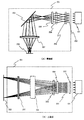
本発明の実施形態の一つについて説明する。図1(A)は本発明のレーザー装置の構成を示す図である。このレーザー装置は、レーザー101、レーザー101を発振源とするレーザー光を線状に変形する光学系201、透光性基板を固定するステージ102を有し、ステージ102にはヒータ103とヒータコントローラー104が具備されて、基板を室温〜550℃の範囲の温度に保持することができる。また、ステージ102上には反射体105が設けられ、その上に非晶質半導体膜が形成された基板106が設置される。
【0035】
次に、図1(A)のような構成のレーザー装置において、基板106の保持方法を図1(B)を用いて説明する。ステージ102に保持された基板106は、反応室107に設置され、レーザー101を発振源とする線状のレーザー光が照射される。反応室内は図示されていない排気系またはガス系により減圧状態または不活性ガス雰囲気とすることができ、半導体膜を汚染させることなく100〜450℃まで加熱することができる。
【0036】
また、ステージ102はガイドレール108に沿って反応室内を移動することができ、基板の全面に線状のレーザー光を照射することができる。レーザー光は基板106の上面に設けられた図示されていない石英製の窓から入射する。また、図1(B)ではこの反応室107にトランスファー室109、中間室110、ロード・アンロード室111が接続され、それぞれの室は仕切弁112、113で分離されている。
【0037】
ロード・アンロード室111には複数の基板を保持することが可能なカセット114が設置され、トランスファー室109に設けられた搬送ロボット115により基板が搬送される。基板106'は搬送中の基板を表す。このような構成とすることによりレーザーアニールを減圧下または不活性ガス雰囲気中で連続して処理することができる。
【0038】
次に、レーザー光を線状にする光学系201の構成について図2を用いて説明する。図2(A)は光学系201を側面から見た図であり、図2(B)は光学系201を上面から見た図である。
【0039】
レーザー101を発振源とするレーザー光はシリンドリカルレンズアレイ202により縦方向に分割される。この分割されたレーザー光はシリンドリカルレンズ203によりさらに横方向に分割される。即ち、レーザー光はシリンドリカルレンズアレイ202、203によって最終的にはマトリクス状に分割されることになる。
【0040】
そして、レーザー光はシリンドリカルレンズ204により一旦集光される。その際、シリンドリカルレンズ204の直後にシリンドリカルレンズ205を通る。その後、ミラー206で反射され、シリンドリカルレンズ207を通った後、照射面208に達する。
【0041】
このとき、照射面208に投影されたレーザー光は線状の照射面を示す。即ち、シリンドリカルレンズ207を透過したレーザー光の断面形状は線状になっていることを意味する。この線状に変形されたレーザー光の幅方向(短い方向)の均質化は、シリンドリカルレンズアレイ202、シリンドリカルレンズ204及びシリンドリカルレンズ207で行われる。また、上記レーザー光の長さ方向(長い方向)の均質化は、シリンドリカルレンズアレイ203及びシリンドリカルレンズ205で行われる。
【0042】
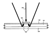
次に、基板上に形成された被処理膜の表面及び裏面からレーザー光を照射するための構成について図3を用いて説明する。図3に示したのは、図1における基板106と反射体105との位置関係を示す図である。
【0043】
図3において、301は透光性基板であり、その表面(薄膜または素子が形成される側の面)には絶縁膜302、非晶質半導体膜(または微結晶半導体膜)303が形成されている。また、透光性基板301の下にはレーザー光を反射させるための反射体304が配置される。
【0044】
透光性基板301はガラス基板、石英基板、結晶化ガラス基板若しくはプラスチック基板が用いられる。この透光性基板301自体で第二次レーザー光の実効エネルギー強度を調節することが可能である。また、絶縁膜302は酸化シリコン膜や窒化酸化シリコン膜(SiOxNy)などの珪素を含む絶縁膜を用いれば良く、この絶縁膜302で第二次レーザー光の実効エネルギー強度を調節しても良い。また、非晶質半導体膜303はアモルファスシリコン膜の他に、アモルファスシリコンゲルマニウム膜などの化合物半導体膜も含む。
【0045】
また、反射体304は表面(レーザー光の反射面)に金属膜を形成した基板であっても良いし、金属元素でなる基板であっても良い。この場合、金属膜としては如何なる材料を用いても良い。代表的には、シリコン(Si)、アルミニウム(Al)、銀(Ag)、タングステン(W)、チタン(Ti)、タンタル(Ta)のいずれかの元素を含む金属膜を用いる。例えば、窒化タングステン(WN)、窒化チタン(TiN)、窒化タンタル(TaN)を用いても良い。
【0046】
さらに、この反射体304は透光性基板301に接して設けても良いし、離して設けても良い。また、反射体304を配置する代わりに、基板301の裏面(表面の反対側の面)に直接上述のような金属膜を形成し、そこでレーザー光を反射させることも可能である。いずれにしても、この反射体304の反射率で第二次レーザー光の実効エネルギー強度を調節することができる。また、反射体304を透光性基板301と離して設置する場合、その隙間に充填する気体(ガス)で第二次レーザー光のエネルギー強度を制御することも可能である。
【0047】
そして、図2で説明した光学系201を経由して線状に変形されたレーザー光が、非晶質半導体膜303に照射される。この線状に変形されたレーザー光の照射はレーザー光を走査することによって行われる。
【0048】
いずれにしても、シリンドリカルレンズ207を透過して非晶質半導体膜303の表面に照射される第一次レーザー光305と、反射体304で一旦反射されて非晶質半導体膜303の裏面に照射される第二次レーザー光306との実効エネルギー強度比(I0'/I0)が、0<I0'/I0<1または1<I0'/I0の関係を満たすことが重要である。このためには、反射体304のレーザー光に対する反射率は20〜80%であることが好ましい。また、このとき、本実施形態でいくつか述べた第二次レーザー光の実効エネルギー強度を減衰させる手段を、複数組み合わせて所望の強度比としても良い。
【0049】
また、シリンドリカルレンズ207を通過したレーザー光は、集光される過程で基板表面に対して45〜90°の入射角を持つ。そのため、第二次レーザー光306は非晶質半導体膜303の裏面側にも回り込んで照射される。また、反射体304の反射面に起伏部を設けてレーザー光を乱反射させることで、第二次レーザー光306をさらに効率良く得ることができる。
【0050】
〔実施形態2〕
本実施形態ではの実施形態1と異なる実施の形態について説明する。本実施形態では、実施形態1のような反射体を用いず、光学系の途中で分光した二系統のレーザー光を非晶質半導体膜の表面及び裏面から照射する例を示す。
【0051】
図4(A)は本実施形態のレーザー装置の構成を示す図である。基本的な構成は実施形態1で説明した図1のレーザー装置と同様であるので異なる部分の符号を変えて説明する。
【0052】
このレーザー装置は、レーザー101、レーザー101を発振源とするレーザー光を線状に変形し、且つ、二系統に分光する光学系401、透光性基板を固定する透光性のステージ402を有する。また、ステージ402上には基板403aが設置され、その上に非晶質半導体膜403bが形成されている。
【0053】
本実施形態の場合、ステージ402を透過したレーザー光を非晶質半導体膜403bに照射するため、ステージ402は透光性を有してなければならない。また、ステージ402側から照射されるレーザー光(第二次レーザー光)はステージ402を透過するので、その実効エネルギー強度はステージ402を透過する際の減衰を考慮しなければならない。
【0054】
また、図4(B)は図4(A)に示したレーザー装置における基板403aの保持方法を説明する図面であるが、透光性ステージ402を用いること以外は図1(B)に示した構成と同一であるので説明は省略する。
【0055】
次に、図4(A)に示した光学系401の構成について図5を用いて説明する。図5は光学系401を側面から見た図である。レーザー501を発振源とするレーザー光はシリンドリカルレンズアレイ502により縦方向に分割される。この分割されたレーザー光はシリンドリカルレンズ503によりさらに横方向に分割される。こうしてレーザー光はシリンドリカルレンズアレイ502、503によってマトリクス状に分割される。
【0056】
そして、レーザー光はシリンドリカルレンズ504により一旦集光される。その際、シリンドリカルレンズ504の直後にシリンドリカルレンズ505を通る。ここまでは図2に示した光学系と同様である。
【0057】
その後、レーザー光はハーフミラー506に入射し、ここでレーザー光は第一次レーザー光507と第二次レーザー光508とに分光される。そして、第一次レーザー光507はミラー509、510で反射され、シリンドリカルレンズ511を通った後、非晶質半導体膜403bの表面に達する。
【0058】
また、ハーフミラー506で分光された第二次レーザー光508はミラー512、513、514で反射され、シリンドリカルレンズ515を通った後、基板403aを透過して非晶質半導体膜403bの裏面に達する。
【0059】
このとき、実施形態1と同様に基板の照射面に投影されたレーザー光は線状の照射面を示す。また、この線状に変形されたレーザー光の幅方向(短い方向)の均質化は、シリンドリカルレンズアレイ502、シリンドリカルレンズ504及びシリンドリカルレンズ515で行われる。また、上記レーザー光の長さ方向(長い方向)の均質化は、シリンドリカルレンズアレイ503、シリンドリカルレンズ505及びシリンドリカルレンズ511で行われる。
【0060】
いずれにしても、シリンドリカルレンズ511を透過して非晶質半導体膜403bの表面に照射される第一次レーザー光と、シリンドリカルレンズ515を透過して非晶質半導体膜403bの裏面に照射される第二次レーザー光との実効エネルギー強度比(I0'/I0)が、0<I0'/I0<1または1<I0'/I0の関係を満たすことが重要である。
【0061】
本実施形態では基板403aとしてガラス基板(ここで用いるレーザー光の透過率が約50%の材料でなるもの)を用いることで、上述の関係式を満たすようにしている。勿論、基板以外にも基板403a上に設けた絶縁膜(図示せず)や、基板403aを設置するステージ(図示せず)の透過率や界面の反射率を調節して第二次レーザー光の実効エネルギー強度を減衰させても良い。
【0062】
また、光学系401の第二次レーザー光の光路において、任意の場所に減光フィルターを設けて、第二次レーザー光の実効エネルギー強度を減衰させることも可能であるし、逆に光学系401の第一次レーザー光の光路において、任意の場所に減光フィルターを設けて、第一次レーザー光の実効エネルギー強度を減衰させることも可能である。
【0063】
また、本実施形態でいくつか述べた第一次レーザー光もしくは第二次レーザー光の実効エネルギー強度を減衰させる手段を、複数組み合わせて所望の強度比としても良い。
【実施例】
〔実施例1〕
本実施例では、実施形態1に示した構成でアモルファスシリコン膜の結晶化を行った例を示す。説明には図3を用いる。
【0064】
本実施例では、基板301として1.1mm厚の石英基板、絶縁膜302として200nm厚の窒化酸化シリコン膜(SiON膜)、非晶質半導体膜303としてアモルファスシリコン膜を用いた。このとき、SiON膜302とアモルファスシリコン膜303はプラズマCVD法を用いて形成した。
【0065】
本実施例では、まずSiH4を4SCCM、N2Oを400SCCMとして反応室に導入し、成膜温度400℃、反応圧力30Pa、放電電力密度0.41W/cm2、放電周波数60MHzとしてSiON膜302を形成した。次に、SiH4を100SCCMで反応室に導入し、成膜温度300℃、反応圧力45Pa、放電電力密度0.037W/cm2、放電周波数13.56MHzとしてアモルファスシリコン膜303を形成した。なお、実際にはアモルファスシリコン膜をパターニングして島状パターンとした。
【0066】
次に、図1(B)に示したようなエキシマレーザー装置を用いてアモルファスシリコン膜303のレーザー結晶化を行った。このとき、図3の反射体304としては、シリコン基板上に窒化タングステン膜を形成したものを用いた。また、反射体304と石英基板301との間には150μmの隙間を空けた。
【0067】
この状態で図3に示すようにエキシマレーザー光(第一次レーザー光305と第二次レーザー光306)をアモルファスシリコン膜303に対して室温、大気雰囲気中で照射した。エキシマレーザー光は図2に示した光学系により断面形状を線状(0.4mm×160mm)に変形し、基板の一端から他端まで走査した。また、走査速度は1mm/sとし、エネルギー密度(図6のIaに想到するエネルギー強度)は336mJ/cm2、パルス幅は30ns、繰り返し周波数は30Hz、重ね合わせ率は90%とした。これにより一カ所に20ショットのレーザー光を照射することができた。
【0068】
なお、本実施例の構成でレーザー結晶化を行う場合、第一次レーザー光の実効エネルギー強度(I0)は151.2mJ/cm2であり、第二次レーザー光の実効エネルギー強度(I0')は77.3mJ/cm2であった。従って、実効エネルギー強度比(I0'/I0)は0.51であった。
【0069】
ここで本実施例に従って結晶化させたポリシリコン膜のSEM写真を図10に示す。なお、図10はセコ・エッチング後の状態である。このセコ・エッチングはフッ化水素酸溶液50ccと水25ccと1.14gのクロム酸カリウム(二価)とを加えた室温のエッチャントを用いた。
【0070】
その結果、図10に示すように、島状パターンの中心付近に平均結晶粒径が0.5〜0.6μm程度の比較的大きな結晶粒が確認できた。島状パターンの端部には結晶粒径の小さな結晶粒が存在するが、レーザーエネルギー密度を変えることで形成される位置が変化する。実際に本実施例によって形成したポリシリコン膜をTFTの活性層として用いる場合には、このような結晶粒径の小さな部分がチャネル形成領域に当たらないように設計すれば良い。
【0071】
〔実施例2〕
本実施例では、実施形態1に示した構成でアモルファスシリコン膜の結晶化を行った例を示す。なお、本実施例で行ったレーザー結晶化は実施例1において反射体304の表面に形成する膜をタングステン膜に、レーザーエネルギー密度を369mJ/cm2に変更しただけであるので、他の条件の詳細な説明は実施例1を参考にすれば良い。
【0072】
本実施例に従って結晶化させたポリシリコン膜のSEM写真を図11に示す。なお、実施例1と同様に図11はセコ・エッチング後の状態である。セコ・エッチングの条件は実施例1を参考にすれば良い。
【0073】
なお、本実施例の構成でレーザー結晶化を行う場合、第一次レーザー光の実効エネルギー強度(I0)は166.1mJ/cm2であり、第二次レーザー光の実効エネルギー強度(I0')は88.6mJ/cm2であった。従って、実効エネルギー強度比(I0'/I0)は0.53であった。
【0074】
その結果、図11に示すように、島状パターン全体に平均結晶粒径が0.6〜0.7μm程度の比較的大きな結晶粒が確認できた。なお、図11では図10に見られたような島状パターンの端部の小さな結晶粒は顕著に見られなかった。しかしながら、レーザーエネルギー密度を変えることで顕著に見られる条件もあったため、レーザーエネルギー密度の最適化が必要である。また、結晶粒径の小さな部分があっても、実施例1と同様にTFTのチャネル形成領域に当たらないように設計すれば問題はない。
【0075】
〔実施例3〕
本実施例では、実施形態1に示した構成でアモルファスシリコン膜の結晶化を行った例を示す。なお、本実施例で行ったレーザー結晶化は実施例1において反射体304の表面に形成する膜を窒化チタン膜に、レーザーエネルギー密度を384mJ/cm2に変更しただけであるので、他の条件の詳細な説明は実施例1を参考にすれば良い。
【0076】
本実施例に従って結晶化させたポリシリコン膜のSEM写真を図12に示す。なお、実施例1と同様に図12はセコ・エッチング後の状態である。セコ・エッチングの条件は実施例1を参考にすれば良い。
【0077】
なお、本実施例の構成でレーザー結晶化を行う場合、第一次レーザー光の実効エネルギー強度(I0)は172.8mJ/cm2であり、第二次レーザー光の実効エネルギー強度(I0')は57.6mJ/cm2であった。従って、実効エネルギー強度比(I0'/I0)は0.33であった。
【0078】
その結果、図12に示すように、島状パターン全体に平均結晶粒径が0.8〜1.0μm程度の大きな結晶粒が確認できた。この結晶粒は紙面に向かって横方向に長い形状であり、島状パターンの横方向の端部から結晶化が進行した可能性を示唆するものと思われる。この傾向は図11においても若干確認される。
【0079】
また、やはりレーザーエネルギー密度を変えることで顕著に見られる条件もあったため、レーザーエネルギー密度の最適化が必要である。また、結晶粒径の小さな部分があっても、実施例1と同様にTFTのチャネル形成領域に当たらないように設計すれば問題はない。
【0080】
〔実施例4〕
本実施例では、実施形態1または実施形態2の方法により、TFTの活性層となるポリシリコン膜を形成する例について説明する。説明には図13を用いる。
【0081】
まず、ガラス基板上に厚さ200nmの窒化酸化シリコン膜(図示せず)を形成し、その上に50nm厚のアモルファスシリコン膜(図示せず)を形成する。次に、アモルファスシリコン膜をパターニングしてアモルファスシリコン膜でなる島状パターン1301a、1301bを形成する。(図13(A))
【0082】
次に、島状パターン1301a、1301bを、実施形態1または実施形態2の方法によってレーザー結晶化する。レーザー結晶化によって得られたポリシリコン膜でなる島状パターン1302a、1302bは端部に結晶粒の小さな領域1303a、1303bを有することがある。また、島状パターン1302a、1302bの端部は結晶欠陥や格子歪みを多く含む領域でもある。(図13(B))
【0083】
なお、1304a、1304bで示された点線は、アモルファスシリコン膜でなる島状パターン1301a、1301bの跡であり、レーザー結晶化によって島状パターンが1〜15%ほど縮小化することを意味する。この縮小化はシリコン膜の緻密化と気化によって起こると考えられるが詳細は明らかではない。
【0084】
また、この島状パターン1301a、1301bの跡1304a、1304bは、下に形成された窒化酸化シリコン膜(図示せず)の段差となって残る。
【0085】
次に、ポリシリコン膜でなる島状パターン1302a、1302bを再びパターニングして活性層1305a、1305bを形成する。なお、1306a、1306bで示された点線は結晶粒の小さな領域1303a、1303bの跡である。また、活性層1305a、1305bを形成することによって下に形成された窒化酸化シリコン膜(図示せず)には再び段差が形成される。
(図13(C))
【0086】
即ち、前工程で形成された島状パターン1301a、1301bの形状に沿って形成された第1の段差と、活性層1305a、1305bの形状に沿って形成された第2の段差とが、ガラス基板上の窒化酸化シリコン膜に形成されることになる。このように、まず第1の形状の半導体パターンを形成した後にレーザー結晶化し、第1の形状の半導体パターンをさらにパターニングして第2の形状の半導体パターンを形成する技術は特開平8−228006号公報に開示されている。この技術を使うと上述のような二つの段差が残る。
【0087】
次に、活性層1305a、1305bを覆って80nm厚の窒化酸化シリコン膜でなるゲート絶縁膜を形成し、その上にゲート電極1307を形成する。ゲート電極1307は窒化タングステン膜とタングステン膜との積層構造で形成し、膜厚は300nmとする。(図13(D))
【0088】
ゲート電極1307を形成したら、n型を付与する不純物元素の添加工程を行い、ソース領域1308a、ドレイン領域1309a、LDD領域1310を形成する。さらに、選択的にp型を付与する不純物元素の添加工程を行い、ソース領域1308b、ドレイン領域1309bを形成する。また同時に、チャネル形成領域1311a、1311b(活性層のうち不純物元素が添加されなかった領域)が形成される。
【0089】
次に、酸化シリコン膜でなる層間絶縁膜(図示せず)を1μmの厚さに形成した後、コンタクトホールを開けて、ソース配線1312a、1312b、ドレイン配線1313を形成する。これら配線はアルミニウム膜を主体とする低抵抗な導電膜で形成すれば良い。(図13(E))
【0090】
以上の工程によって、図13(E)に示すような構造のnチャネル型TFT1314及びpチャネル型TFT1315を相補的に組み合わせたCMOS回路1316が形成される。
【0091】
なお、本実施例は本発明をTFTの活性層を形成する際に実施した一実施例であり、この作製工程に限定する必要はない。本発明は、公知のあらゆるTFTの作製工程に用いることができる。但し、活性層の下に遮光膜等を設ける場合、即ち、非晶質半導体膜の表面及び裏面を同時にレーザーアニールすることが不可能な場合を除く。
【0092】
また、本実施例ではCMOS回路を形成する例を示しているが、アクティブマトリクス型画像表示装置の画素部に設けられる画素TFTも、公知の技術を用いれば容易に作製することが可能である。
【0093】
〔実施例5〕
本実施例では、実施形態1または実施形態2によって形成した結晶質半導体膜を、TFTの活性層として用いる場合の配置について説明する。
【0094】
実施例2の条件において、レーザー密度を384mJ/cm2に変更してレーザーアニールを行って得たポリシリコン膜は、図26に示すような状態で結晶粒が分布していることが確認できた。即ち、島状パターンの端部に平均結晶粒径の大きな第1の領域が形成され、中央部に第1の領域よりも平均結晶粒径の小さな第2の領域が形成される。なお、第2の領域の平均結晶粒径は第1の平均結晶粒径に比べて1/3以下である。このような場合、図14(A)に示すように中心部の第2の領域を使わないように活性層の配置を設計する必要がある。
【0095】
図14(A)において、1401は本実施例の条件で形成された島状パターンの模式図であり、1402は第2の領域である。また、1403a、1403bは第1の領域(活性層として用いる領域)であり、1404a、1404bで示される点線は活性層が形成される部分に対応する。
【0096】
また、図14(B)のように、図14(A)のように配置された活性層を有する二種類のTFT(nチャネル型TFTとpチャネル型TFT)を組み合わせてCMOS回路を形成することも可能である。
【0097】
図14(B)において、nチャネル型TFT1405は、ゲート電極1406、ソース領域1407a、ドレイン領域1408a、LDD領域1409、チャネル形成領域1410a、ソース配線1411a及びドレイン配線1412で構成される。また、pチャネル型TFT1413は、ゲート電極1406、ソース領域1407b、ドレイン領域1408b、チャネル形成領域1410b、ソース配線1411b及びドレイン配線1412で構成される。
【0098】
そして、nチャネル型TFT1405とpチャネル型TFT1413とでゲート電極1406及びドレイン配線1412を共通化して、CMOS回路を形成することができる。勿論、これ以外の電気回路または電気素子を形成することも可能である。
【0099】
なお、実施例4でも述べたように、本実施例を実施すると島状パターン1401に対応する段差及び活性層1404a、1404bに対応する段差が、ポリシリコン膜の下地となる絶縁膜(または基板)に形成される。これは本実施例を実施した場合の特徴と言える。
【0100】
図14(A)と図14(B)に共通な概念は、結晶粒径の大きな第1の領域に少なくともチャネル形成領域が形成されるように活性層を配置することである。チャネル形成領域に含まれる結晶粒界が1本、好ましくは0本となるように配置することが最も好ましい。そうすることでTFTの電界効果移動度やしきい値電圧といった代表的な電気特性を改善することが可能である。
【0101】
〔実施例6〕
本実施例では、実施例5の図26で説明したような結晶状態の島状パターンから活性層を切り出してTFTを作製する場合について説明する。具体的には画素部の画素TFTおよび保持容量と、画素部の周辺に設けられる駆動回路のnチャネル型TFTとpチャネル型TFTとを同時に作製する方法について説明する。説明には図15〜図17を用いる。
【0102】
図15(A)において、基板701にはコーニング社の#7059ガラスや#1737ガラスなどに代表されるバリウムホウケイ酸ガラスやアルミノホウケイ酸ガラスなどのガラス基板の他に、ポリエチレンテレフタレート(PET)、ポリエチレンナフタレート(PEN)、ポリエーテルサルフォン(PES)など光学的異方性を有しないプラスチック基板を用いることができる。また、石英基板や結晶化ガラス基板を用いても良い。
【0103】
そして、基板701のTFTを形成する表面に、基板701からの不純物拡散を防ぐために、酸化シリコン膜、窒化シリコン膜または酸化窒化シリコン膜などの下地膜702を形成する。本実施例ではプラズマCVD法でSiH4、NH3、N2Oから作製される酸化窒化シリコン膜702aを10〜200nm(好ましくは50〜100nm)、同様にSiH4、N2Oから作製される酸化窒化水素化シリコン膜702bを50〜200nm(好ましくは100〜150nm)の厚さに積層形成する。
【0104】
酸化窒化シリコン膜は従来の平行平板型のプラズマCVD法を用いて形成する。酸化窒化シリコン膜702aは、SiH4を10SCCM、NH3を100SCCM、N2Oを20SCCMとして反応室に導入し、基板温度325℃、反応圧力40Pa、放電電力密度0.41W/cm2、放電周波数60MHzとする。一方、酸化窒化水素化シリコン膜702bは、SiH4を5SCCM、N2Oを120SCCM、H2を125SCCMとして反応室に導入し、基板温度400℃、反応圧力20Pa、放電電力密度0.41W/cm2、放電周波数60MHzとする。これらの膜は、基板温度を変化させ、反応ガスの切り替えのみで連続して形成することもできる。
【0105】
また、酸化窒化シリコン膜702aは基板を中心に考えて、その内部応力が引張り応力となるように形成する。酸化窒化シリコン膜702bも同様な方向に内部応力を持たせるが、酸化窒化シリコン膜702aよりも絶対値で比較して小さい応力となるようにする。
【0106】
次に、25〜80nm(好ましくは30〜60nm)の厚さで非晶質半導体膜703を、プラズマCVD法やスパッタ法などの公知の方法で形成する。例えば、プラズマCVD法で非晶質シリコン膜を55nmの厚さに形成する。このとき、下地膜702と非晶質半導体膜703とは両者を連続形成することも可能である。例えば、前述のように酸化窒化シリコン膜702aと酸化窒化水素化シリコン膜702bをプラズマCVD法で連続して成膜後、反応ガスをSiH4、N2O、H2からSiH4とH2或いはSiH4のみに切り替えれば、一旦大気雰囲気に晒すことなく連続形成できる。その結果、酸化窒化水素化シリコン膜702bの表面の汚染を防ぐことが可能となり、作製するTFTの特性バラツキやしきい値電圧の変動を低減させることができる。
【0107】
そして、まず非晶質構造を有する半導体層703から、図15(B)で点線で示すように第1の形状を有する島状半導体層704〜706を形成する。図18(A)はこの状態における島状半導体層704の上面図であり、同様に図19(A)は島状半導体層706の上面図を示す。
【0108】
図18および図19において、島状半導体層は長方形とし一辺が50μm以下となるように形成するが、島状半導体層の形状は任意なものとすることが可能で、好ましくはその中心部から端部までの最小距離が50μm以下となるような形態であればどのような多角形、或いは円形とすることもできる。
【0109】
次に、このような島状半導体層704〜706に対して結晶化の工程を行う。結晶化の工程は、実施形態1または2で説明したどちらの方法を用いることも可能であるが、本実施例では実施形態1の方法で島状半導体層704〜706にレーザーアニールを行う。こうして図15(B)の実線で示す結晶質シリコン膜から成る島状半導体層707〜711が形成される。
【0110】
なお、本実施例では二つのTFTに対応して一つの島状半導体層を形成する例を示しているが、島状半導体層の専有面積が大きくなる場合(一つのTFTの大きさが大きくなる場合)には、複数の島状半導体層に分割し、複数のTFTを直列に接続したものを一つのTFTとして機能させることも可能である。
【0111】
このとき、非晶質シリコン膜の結晶化に伴って膜が緻密化し、1〜15%程度収縮する。そして、島状半導体層の端部には収縮により歪みが発生した領域712が形成される。さらに、島状半導体層の中央部には結晶粒の小さな領域(平均結晶粒径の小さな領域)713が形成される。図18(B)および図19(B)は、それぞれこの状態の島状半導体層の上面図を示す。同図中で点線で示す領域704、706は元々あった島状半導体層704、706の大きさを示す。
【0112】
このように歪みが蓄積した領域712や結晶粒が小さい領域713がチャネル形成領域に含まれてしまうと、多数の欠陥準位によりTFTの特性を劣化させる原因となる。例えば、オフ電流値が増大したり、この領域に電流が集中して局部的に発熱したりするため好ましくない。
【0113】
従って、図15(C)で示すように、上述のような領域が除去されるように第2の形状の島状半導体層715、716を形成する。但し、図19に示すように画素TFTの活性層となる島状半導体層719の場合、ソース領域、ドレイン領域及び保持容量の電極として働く領域に、上述の結晶粒が小さい領域713が含まれている。このような結晶粒が小さい領域はチャネル形成領域にさえ含まれていなければ問題とはならない。
【0114】
なお、図中点線で示す714'は歪みが蓄積した領域712や結晶粒が小さい領域713が存在していた領域であり、その領域より内側に第2の形状の島状半導体層715、716、719を形成する状態を示している。この第2の形状の島状半導体層715、716、719の形状は任意な形状のものとすれば良い。図18(C)にはこの状態における島状半導体層715、716の上面図を示す。また、同様に図19(C)には島状半導体層719の上面図を示す。
【0115】
その後、この島状半導体層715〜719を覆って、プラズマCVD法またはスパッタ法により50〜100nmの厚さの酸化シリコン膜によるマスク層720を形成する。この状態で島状半導体層に対し、TFTのしきい値電圧(Vth)を制御する目的でp型を付与する不純物元素を1×10¹⁶〜5×10¹⁷atoms/cm3程度の濃度で島状半導体層の全面に添加しても良い。
【0116】
半導体に対してp型を付与する不純物元素には、ホウ素(B)、アルミニウム(Al)、ガリウム(Ga)など周期律表第13族の元素が知られている。その方法として、イオン注入法やイオンドープ法を用いることができるが、大面積基板を処理するにはイオンドープ法が適している。イオンドープ法ではジボラン(B2H6)をソースガスとして用いホウ素(B)を添加する。このような不純物元素の注入は必ずしも必要でなく省略しても差し支えないが、特にnチャネル型TFTのしきい値電圧を所定の範囲内に収めるためには有効である。
【0117】
駆動回路のnチャネル型TFTのLDD領域を形成するために、n型を付与する不純物元素を島状半導体層716、718に選択的に添加する。そのため、あらかじめレジストマスク721a〜721eを形成する。n型を付与する不純物元素としては、リン(P)や砒素(As)を用いれば良く、ここではリン(P)を添加すべく、フォスフィン(PH3)を用いたイオンドープ法を用いる。
【0118】
形成された不純物領域は低濃度n型不純物領域722、723として、このリン(P)濃度は2×10¹⁶〜5×10¹⁹atoms/cm3の範囲とすれば良い。本明細書中では、ここで形成された不純物領域722、723に含まれるn型を付与する不純物元素の濃度を(n-)と表す。また、不純物領域724は、画素部の保持容量を形成するための半導体層であり、この領域にも同じ濃度でリン(P)が添加される(図15(D))。
【0119】
次に、添加した不純物元素を活性化させる工程を行う。活性化は、窒素雰囲気中で500〜600℃で1〜4時間の熱処理や、レーザー活性化の方法により行うことができる。また、両者を併用して行っても良い。レーザー活性化の方法による場合、KrFエキシマレーザー光(波長248nm)を用い、線状ビームを形成して、発振周波数5〜50Hz、エネルギー密度100〜500mJ/cm2として線状ビームのオーバーラップ割合を80〜98%として走査して、島状半導体層が形成された基板全面を処理する。尚、レーザー光の照射条件には何ら限定される事項はなく、実施者が適宣決定すれば良い。この工程は、マスク層720を残して行っても良いし、除去してから行っても良い。
【0120】
図15(E)において、ゲート絶縁膜725はプラズマCVD法またはスパッタ法を用い、膜厚を40〜150nmとしてシリコンを含む絶縁膜で形成する。例えば、120nmの厚さで酸化窒化シリコン膜から形成すると良い。また、SiH4とN2OにO2を添加させて作製された酸化窒化シリコン膜は、膜中の固定電荷密度が低減されているのでこの用途に対して好ましい材料となる。勿論、ゲート絶縁膜725はこのような酸化窒化シリコン膜に限定されるものでなく、他のシリコンを含む絶縁膜を単層または積層構造として用いても良い。いずれにしても、ゲート絶縁膜725は基板を中心に考え圧縮応力となるように形成する。
【0121】
そして、図15(E)に示すように、ゲート絶縁膜725上にゲート電極を形成するための耐熱性導電層を形成する。耐熱性導電層は単層で形成しても良いが、必要に応じて二層あるいは三層といった複数の層から成る積層構造としても良い。このような耐熱性導電性材料を用い、例えば、導電性の窒化物金属膜から成る導電層(A)726と金属膜から成る導電層(B)727とを積層した構造とすると良い。
【0122】
導電層(B)727はタンタル(Ta)、チタン(Ti)、モリブデン(Mo)、タングステン(W)から選ばれた元素、または前記元素を主成分とする合金か、前記元素を組み合わせた合金膜(代表的にはMo−W合金膜、Mo−Ta合金膜)で形成すれば良く、導電層(A)726は窒化タンタル(TaN)、窒化タングステン(WN)、窒化チタン(TiN)膜、窒化モリブデン(MoN)などで形成する。また、導電層(A)726はタングステンシリサイド、チタンシリサイド、モリブデンシリサイドを適用しても良い。
【0123】
また、導電層(B)727は低抵抗化を図るために含有する不純物濃度を低減させることが好ましく、特に酸素濃度に関しては30ppm以下とすることが好ましい。例えば、タングステン(W)は酸素濃度を30ppm以下とすることで20μΩcm以下の比抵抗値を実現することができる。
【0124】
導電層(A)726は10〜50nm(好ましくは20〜30nm)とし、導電層(B)727は200〜400nm(好ましくは250〜350nm)とすれば良い。Wをゲート電極とする場合には、Wをターゲットとしたスパッタ法で、アルゴン(Ar)ガスと窒素(N2)ガスを導入して導電層(A)726を窒化タングステン(WN)で50nmの厚さに形成し、導電層(B)727をWで250nmの厚さに形成する。その他の方法として、W膜は6フッ化タングステン(WF6)を用いて熱CVD法で形成することもできる。
【0125】
いずれにしてもゲート電極として使用するためには低抵抗化を図る必要があり、W膜の抵抗率は20μΩcm以下にすることが望ましい。W膜は結晶粒を大きくすることで低抵抗率化を図ることができるが、W中に酸素などの不純物元素が多い場合には結晶化が阻害され高抵抗化する。このことより、スパッタ法による場合、純度99.9999%のWターゲットを用い、さらに成膜時に気相中からの不純物の混入がないように十分配慮してW膜を形成することにより、抵抗率9〜20μΩcmを実現することができる。
【0126】
一方、導電層(A)726にTaN膜を、導電層(B)727にTa膜を用いる場合には、同様にスパッタ法で形成することが可能である。TaN膜はTaをターゲットとしてスパッタガスにArと窒素との混合ガスを用いて形成し、Ta膜はスパッタガスにArを用いる。また、これらのスパッタガス中に適量のXeやKrを加えておくと、形成する膜の内部応力を緩和して膜の剥離を防止することができる。α相のTa膜の抵抗率は20μΩcm程度でありゲート電極に使用することができるが、β相のTa膜の抵抗率は180μΩcm程度でありゲート電極とするには不向きである。TaN膜はα相に近い結晶構造を持つので、この上にTa膜を形成すればα相のTa膜が容易に得られる。
【0127】
なお、図示しないが、導電層(A)726の下に2〜20nm程度の厚さでリン(P)をドープしたシリコン膜を形成しておくことは有効である。これにより、その上に形成される導電膜の密着性向上と酸化防止を図ると同時に、導電層(A)726または導電層(B)727が微量に含有するアルカリ金属元素がゲート絶縁膜725に拡散するのを防ぐことができる。いずれにしても、導電層(B)727は抵抗率を10〜50μΩcmの範囲とすることが好ましい。
【0128】
次に、フォトマスクを用い、フォトリソグラフィーの技術を使用してレジストマスク728a〜728fを形成し、導電層(A)726と導電層(B)727とを一括でエッチングしてゲート電極729〜733と容量配線734を形成する。ゲート電極729〜733と容量配線734は、導電層(A)から成る729a〜733aと、導電層(B)から成る729b〜733bとが一体として形成されている(図16(A))。
【0129】
また、この状態における島状半導体層715、716とゲート電極729、730との位置関係を図18(D)に示す。同様に島状半導体層719とゲート電極733、容量配線734の関係を図19(D)に示す。図18(D)および図19(D)において、ゲート絶縁膜725は省略する。
【0130】
導電層(A)および導電層(B)をエッチングする方法は実施者が適宣選択すれば良いが、前述のようにWを主成分とする材料で形成されている場合には、高速でかつ精度良くエッチングを実施するために高密度プラズマを用いたドライエッチング法を適用することが望ましい。高密度プラズマを得る方法として、マイクロ波プラズマや誘導結合プラズマ(Inductively Coupled Plasma:ICP)エッチング装置を用いると良い。
【0131】
例えば、ICPエッチング装置を用いたWのエッチング法は、エッチングガスにCF4とCl2の2種のガスを反応室に導入し、圧力0.5〜1.5Pa(好ましくは1Pa)とし、誘導結合部に200〜1000Wの高周波(13.56MHz)電力を印加する。この時、基板が置かれたステージには20Wの高周波電力が印加され、自己バイアスで負電位に帯電することにより、正イオンが加速されて異方性のエッチングを行うことができる。ICPエッチング装置を使用することにより、Wなどの硬い金属膜も2〜5nm/秒のエッチング速度を得ることができる。また、残渣を残すことなくエッチングするためには、10〜20%程度の割合でエッチング時間を増しオーバーエッチングをすると良い。しかし、この時に下地とのエッチングの選択比に注意する必要がある。例えば、W膜に対する酸化窒化シリコン膜(ゲート絶縁膜725)の選択比は2.5〜3であるので、このようなオーバーエッチング処理により、酸化窒化シリコン膜が露出した面は20〜50nm程度エッチングされて実質的に薄くなる。
【0132】
そして、画素TFTのnチャネル型TFTにLDD領域を形成するために、n型を付与する不純物元素添加の工程(n--ドープ工程)を行う。ゲート電極729〜733をマスクとして自己整合的にn型を付与する不純物元素をイオンドープ法で添加すればよい。n型を付与する不純物元素として添加するリン(P)の濃度は1×10¹⁶〜5×10¹⁹atoms/cm3の濃度範囲で添加する。このようにして、図16(B)に示すように島状半導体層に低濃度n型不純物領域735〜739を形成する。
【0133】
次に、nチャネル型TFTにおいて、ソース領域またはドレイン領域として機能する高濃度n型不純物領域の形成を行う(n+ドープ工程)。まず、フォトマスクを用い、レジストのマスク740a〜740dを形成し、n型を付与する不純物元素を添加して高濃度n型不純物領域741〜746を形成する。n型を付与する不純物元素にはリン(P)を用い、その濃度が1×10²⁰〜1×10²¹atoms/cm3の濃度範囲となるようにフォスフィン(PH3)を用いたイオンドープ法で行う(図16(C))。
【0134】
そして、pチャネル型TFTを形成する島状半導体層715、717にソース領域およびドレイン領域とする高濃度p型不純物領域748、749を形成する。ここでは、ゲート電極729、731をマスクとしてp型を付与する不純物元素を添加し、自己整合的に高濃度p型不純物領域を形成する。このとき、nチャネル型TFTを形成する島状半導体膜716、718、719は、フォトマスクを用いてレジストマスク747a〜747cを形成し全面を被覆しておく。
【0135】
高濃度p型不純物領域748、749はジボラン(B2H6)を用いたイオンドープ法で形成する。この領域のボロン(B)濃度は3×10²⁰〜3×10²¹atoms/cm3となるようにする(図16(D))。
【0136】
この高濃度p型不純物領域748、749には、前工程においてリン(P)が添加されていて、高濃度p型不純物領域748a、749aには1×10²⁰〜1×10²¹atoms/cm3の濃度で、高濃度p型不純物領域748b、749bには1×1016〜5×1019atoms/cm3の濃度でリンが含まれるが、この工程で添加するボロン(B)の濃度を、含まれるリンの濃度の1.5から3倍とすることでpチャネル型TFTのソース領域およびドレイン領域として問題なく機能させることができる。
【0137】
その後、図17(A)に示すように、ゲート電極およびゲート絶縁膜上から保護絶縁膜750を形成する。保護絶縁膜は酸化シリコン膜、酸化窒化シリコン膜、窒化シリコン膜、またはこれらを組み合わせた積層膜で形成すれば良い。いずれにしても保護絶縁膜750は無機絶縁物材料から形成する。保護絶縁膜750の膜厚は100〜200nmとする。
【0138】
ここで、酸化シリコン膜を用いる場合には、プラズマCVD法で、オルトケイ酸テトラエチル(Tetraethyl Orthosilicate:TEOS)とO2とを混合し、反応圧力40Pa、基板温度300〜400℃とし、高周波(13.56MHz)電力密度0.5〜0.8W/cm2で放電させて形成することができる。酸化窒化シリコン膜を用いる場合には、プラズマCVD法でSiH4、N2O、NH3から作製される酸化窒化シリコン膜、またはSiH4、N2Oから作製される酸化窒化シリコン膜で形成すれば良い。この場合の作製条件は反応圧力20〜200Pa、基板温度300〜400℃とし、高周波(60MHz)電力密度0.1〜1.0W/cm2で形成することができる。また、SiH4、N2O、H2から作製される酸化窒化水素化シリコン膜を適用しても良い。窒化シリコン膜も同様にプラズマCVD法でSiH4、NH3から作製することが可能である。このような保護絶縁膜は、基板を中心に考えて圧縮応力となるように形成する。
【0139】
その後、それぞれの濃度で添加されたn型またはp型を付与する不純物元素を活性化する工程を行う。この工程は電熱炉を用いるファーネスアニール法で行う。その他に、レーザーアニール法、またはラピッドサーマルアニール法(RTA法)を適用することができる。ファーネスアニール法では酸素濃度が1ppm以下、好ましくは0.1ppm以下の窒素雰囲気中で400〜700℃、代表的には500〜600℃で行うことが好ましく、本実施例では550℃で4時間の熱処理を行う。また、基板701に耐熱温度が低いプラスチック基板を用いる場合にはレーザーアニール法を用いる(図17(B))。
【0140】
活性化の工程の後、さらに、3〜100%の水素を含む雰囲気中で、300〜450℃で1〜12時間の熱処理を行い、島状半導体層を水素化する工程を行う。この工程は熱的に励起された水素により島状半導体層のダングリングボンドを終端する工程である。水素化の他の手段として、プラズマ水素化(プラズマにより励起された水素を用いる)を行っても良い。また、基板701の耐熱性が許せば300〜450℃の加熱処理により下地膜702の酸化窒化水素化シリコン膜702b、保護絶縁膜750の酸化窒化シリコン膜の水素をに拡散させて島状半導体層を水素化しても良い。
【0141】
活性化および水素化の工程が終了したら、有機絶縁物からなる層間絶縁膜751を1.0〜2.0μmの平均厚を有して形成する。有機絶縁物としては、ポリイミド、アクリル、ポリアミド、ポリイミドアミド、BCB(ベンゾシクロブテン)等を使用することができる。例えば、基板に塗布後、熱重合するタイプのポリイミドを用いる場合には、クリーンオーブンで300℃で焼成して形成する。また、アクリルを用いる場合には、2液性のものを用い、主材と硬化剤を混合した後、スピナーを用いて基板全面に塗布した後、ホットプレートで80℃で60秒の予備加熱を行い、さらにクリーンオーブンで250℃で60分焼成して形成することができる。
【0142】
層間絶縁膜を有機絶縁物で形成することにより、表面を良好に平坦化させることができる。また、有機絶縁物は一般に誘電率が低いので、寄生容量を低減するできる。しかし、吸湿性があり保護膜としての効果は弱いので、本実施例のように、保護絶縁膜750として形成した酸化シリコン膜、酸化窒化シリコン膜、窒化シリコン膜などと組み合わせて用いることが好ましい。
【0143】
その後、フォトマスクを用い、所定のパターンのレジストマスクを形成し、それぞれの島状半導体膜に形成されたソース領域またはドレイン領域に達するコンタクトホールを形成する。コンタクトホールの形成はドライエッチング法により行う。この場合、エッチングガスにCF4、O2、Heの混合ガスを用い有機絶縁物から成る層間絶縁膜751をまずエッチングし、その後、続いてエッチングガスをCF4、O2として保護絶縁膜750をエッチングする。さらに、島状半導体層との選択比を高めるために、エッチングガスをCHF3に切り替えてゲート絶縁膜725をエッチングすることにより、良好にコンタクトホールを形成することができる。
【0144】
そして、導電性の金属膜をスパッタ法や真空蒸着法で形成し、フォトマスクによりレジストマスクを形成し、エッチングによってソース配線752〜756とドレイン配線757〜761を形成する。ドレイン配線762は隣接する画素のドレイン配線を示す。ここで、ドレイン配線761は画素電極として機能するものである。図示していないが、本実施例ではこの電極を、Ti膜を50〜150nmの厚さで形成し、島状半導体層のソースまたはドレイン領域を形成する半導体膜とコンタクトを形成し、そのTi膜上に重ねてアルミニウム(Al)を300〜400nmの厚さで形成して配線とする。
【0145】
図18(E)はこの状態における島状半導体層715、716、ゲート電極729、730、ソース配線752、753およびドレイン配線757、758の上面図を示す。ソース配線752、753は図示されていない層間絶縁膜および保護絶縁膜に設けられたコンタクトホールによって、島状半導体層715、716とそれぞれ830、833で接続している。また、ドレイン配線757、758は831、832で島状半導体層715、716と接続している。
【0146】
同様に、図19(E)では島状半導体層719、ゲート電極733、容量配線734、ソース配線756およびドレイン配線761の上面図を示し、ソース配線756はコンタクト部834で、ドレイン配線761はコンタクト部835でそれぞれ島状半導体層719と接続している。
【0147】
いずれにしても、第1の形状を有する島状半導体層の内側の領域に、歪みが残留している領域を除去して、第2の形状を有する島状半導体層を形成し、TFTを形成する。
【0148】
この状態で水素化処理を行うとTFTの特性向上に対して好ましい結果が得られる。例えば、3〜100%の水素を含む雰囲気中で、300〜450℃で1〜12時間の熱処理を行うと良く、あるいはプラズマ水素化法を用いても同様の効果が得られる。また、このような熱処理により保護絶縁膜750や、下地膜702にに存在する水素を島状半導体膜715〜719に拡散させ水素化をすることもできる。いずれにしても、島状半導体層715〜719中の欠陥密度を1016/cm3以下とすることが望ましく、そのためには水素を5×1018〜5×1019atoms/cm3程度付与することが好ましい。(図17(C))。
【0149】
こうして同一の基板上に、駆動回路のTFTと画素部の画素TFTとを有した基板を完成させることができる。駆動回路には第1のpチャネル型TFT800、第1のnチャネル型TFT801、第2のpチャネル型TFT802、第2のnチャネル型TFT803、画素部には画素TFT804、保持容量805が形成されている。本明細書では便宜上このような基板をアクティブマトリクス基板と呼ぶ。
【0150】
駆動回路の第1のpチャネル型TFT800には、島状半導体膜715にチャネル形成領域806、高濃度p型不純物領域から成るソース領域807a、807b、ドレイン領域808a、808bを有した構造となっている。
【0151】
第1のnチャネル型TFT801には、島状半導体膜716にチャネル形成領域809、ゲート電極730と重なるLDD領域810、ソース領域812、ドレイン領域811を有している。このLDD領域において、ゲート電極730と重なるLDD領域のチャネル長方向の長さは0.5〜3.0μm、好ましくは1.0〜2.0μmとする。nチャネル型TFTにおけるLDD領域の長さをこのようにすることにより、ドレイン領域近傍に発生する高電界を緩和して、ホットキャリアの発生を防ぎ、TFTの劣化を防止することができる。
【0152】
駆動回路の第2のpチャネル型TFT802は同様に、島状半導体膜717にチャネル形成領域813、高濃度p型不純物領域から成るソース領域814a、814b、ドレイン領域815a、815bを有したシングルドレインの構造を有している。
【0153】
第2のnチャネル型TFT803には、島状半導体膜718にチャネル形成領域816、ゲート電極732と一部が重なるLDD領域817、818、ソース領域820、ドレイン領域819が形成されている。このTFTのゲート電極732と重なるLDD領域の長さも0.5〜3.0μm、好ましくは1.0〜2.0μmとする。また、ゲート電極と重ならないLDD領域のチャネル長方向の長さは0.5〜4.0μm、好ましくは1.0〜2.0μmとする。
【0154】
画素TFT804には、島状半導体膜719にチャネル形成領域821、822、LDD領域823〜825、ソースまたはドレイン領域826〜828を有している。LDD領域のチャネル長方向の長さは0.5〜4.0μm、好ましくは1.5〜2.5μmである。さらに、容量配線734と、ゲート絶縁膜と同じ材料から成る絶縁膜と、画素TFT804のドレイン領域828に接続する半導体層829とから保持容量805が形成されている。図17(C)では画素TFT804をダブルゲート構造としたが、シングルゲート構造でも良いし、複数のゲート電極を設けたマルチゲート構造としても差し支えない。
【0155】
図20は画素部のほぼ一画素分を示す上面図である。図中に示すA−A'断面が図17(C)に示す画素部の断面図に対応している。画素TFT804のゲート電極733は、図示されていないゲート絶縁膜を介してその下の島状半導体層719と交差している。図示はしていないが、島状半導体層には、ソース領域、ドレイン領域、LDD領域が形成されている。また、834はソース配線756とソース領域826とのコンタクト部、835はドレイン配線761とドレイン領域828とのコンタクト部である。保持容量805は、画素TFT804のドレイン領域828から延在する半導体層829がゲート絶縁膜を介して容量配線734と重なる領域で形成されている。
【0156】
以上のようにしてアクティブマトリクス基板が完成する。本実施例に従って作製されたアクティブマトリクス基板は、画素部および駆動回路の仕様に応じて適切な構造のTFTを配置している。そのため、このアクティブマトリクス基板を用いた電気光学装置の動作性能と信頼性を向上させることを可能としている。
【0157】
なお、本実施例では画素TFT804のドレイン配線761をそのまま画素電極として用いており、反射型液晶表示装置に対応した構造となっている。しかし、ドレイン配線761に電気的に接続されるように透明導電膜でなる画素電極を形成することで透過型液晶表示装置にも対応できる。
【0158】
また、本実施例は本発明を用いた半導体装置の作製工程の一例であり、本実施例に示した材料や数値範囲に限定する必要はない。さらに、LDD領域の配置なども実施者が適宜決定すれば良い。
【0159】
〔実施例7〕
本実施例では実施例6に従って作製したアクティブマトリクス基板から、アクティブマトリクス型液晶表示装置を作製する工程を説明する。まず、図21(A)に示すように、図17(C)の状態のアクティブマトリクス基板にパターニングにより樹脂材料でなるスペーサ901a〜901fを形成する。なお、スペーサとして公知の球状シリカ等を散布して用いることもできる。
【0160】
本実施例では、樹脂材料でなるスペーサ901a〜901fとしてJSR社製のNN700を用い、スピナーで塗布した後、露光と現像処理によって所定のパターンに形成する。さらにクリーンオーブンなどで150〜200℃で加熱して硬化させる。このようにして作製されるスペーサは露光と現像処理の条件によって形状を異ならせることができるが、好ましくは、柱状で頂部が平坦な形状となるようにすると、対向側の基板を合わせたときに液晶表示パネルとしての機械的な強度を確保することができる。
【0161】
また、形状は円錐状、角錐状など特別の限定はないが、例えば円錐状としたときに具体的には、高さHを1.2〜5μmとし、平均半径L1を5〜7μm、平均半径L1と底部の半径L2との比を1対1.5とする。このとき側面のテーパー角は±15°以下とする。
【0162】
スペーサ901a〜901fの配置は任意に決定しても良いが、好ましくは、図21(A)で示すように、画素部においてはドレイン配線761(画素電極)のコンタクト部835と重ねてその部分を覆うように形成すると良い。コンタクト部835は平坦性が損なわれこの部分では液晶がうまく配向しなくなるので、コンタクト部835にスペーサ用の樹脂を充填することでディスクリネーションなどを防止することができる。
【0163】
その後、配向膜902を形成する。通常液晶表示素子の配向膜にはポリイミド樹脂を用いる。配向膜を形成した後、ラビング処理を施して液晶分子がある一定のプレチルト角を持って配向するようにする。画素部に設けたスペーサ901a〜901fの端部からラビング方向に対してラビングされない領域が2μm以下となるようにすることが好ましい。また、ラビング処理では静電気の発生がしばしば問題となるが、駆動回路のTFT上において、少なくともソース配線およびドレイン配線上にもスペーサ901a〜901eを形成しておくと、ラビング工程におけるスペーサとしての本来の役割と、静電気からTFTを保護する効果を得ることができる。
【0164】
対向基板903には、遮光膜904、透明導電膜でなる対向電極905および配向膜906を形成する。遮光膜904はTi、Cr、Alなどを150〜300nmの厚さで形成する。そして、画素部と駆動回路が形成されたアクティブマトリクス基板と対向基板とをシール剤907で貼り合わせる。シール剤907にはフィラー908が混合されていて、このフィラー908とスペーサ901a〜901fによって均一な間隔を持って対向基板とアクティブマトリクス基板とが貼り合わせられる。
【0165】
その後、両基板の間に液晶材料909を注入し、封止剤(図示せず)によって完全に封止する。液晶材料には公知の液晶材料を用いれば良い。例えば、TN液晶の他に、電場に対して透過率が連続的に変化する電気光学応答性を示す無しきい値反強誘電性混合液晶を用いることもできる。無しきい値反強誘電性混合液晶にはV字型の電気光学応答特性を示すものもある。詳細は「H.Furue et al.;Charakteristics and Drivng Scheme of Polymer-Stabilized Monostable FLCD Exhibiting Fast Response Time and High Contrast Ratio with Gray-Scale Capability,SID,1998」、「T.Yoshida et al.;A Full-Color Thresholdless Antiferroelectric LCD Exhibiting Wide Viewing Angle with Fast Response Time,841,SID97DIGEST,1997」、「S.Inui et al.;Thresholdless antiferroelectricity in liquid crystals and its application to displays,671-673,J.Mater.Chem.6(4),1996」、または米国特許第5,594,569号を参照すれば良い。
【0166】
このようにして図21(B)に示すアクティブマトリクス型液晶表示装置が完成する。図21ではスペーサ901a〜901eを駆動回路のTFT上の少なくともソース配線およびドレイン配線上にに分割して形成したが、その他に、駆動回路の全面を覆って形成しても差し支えない。
【0167】
図22はアクティブマトリクス基板の上面図を示し、画素部および駆動回路部とスペーサおよびシール剤の位置関係を示す上面図である。画素部1500の周辺に駆動回路として走査信号駆動回路1501と画像信号駆動回路1502が設けられている。さらに、その他CPUやメモリなどの信号処理回路1503も付加されていても良い。
【0168】
そして、これらの駆動回路は接続配線1511によって外部入出力端子1510と接続されている。画素部1500では走査信号駆動回路1501から延在するゲート配線群1504と画像信号駆動回路1502から延在するソース配線群1505がマトリクス状に交差して画素を形成し、各画素にはそれぞれ画素TFT804と保持容量805が設けられている。
【0169】
画素部において設けられるスペーサ1506は、図21で示したスペーサ901fに対応するもので、すべての画素に対して設けても良いが、マトリクス状に配列した画素の数個から数十個おきに設けても良い。即ち、画素部を構成する画素の全数に対するスペーサの数の割合は20〜100%とすると良い。また、駆動回路部に設けるスペーサ1507〜1509はその全面を覆うように設けても良いし、図21で示したように各TFTのソースおよびドレイン配線の位置にあわせて複数個に分割して設けても良い。
【0170】
シール剤907は、基板701上の画素部1500および走査信号制御回路1501、画像信号制御回路1502、その他の信号処理回路1503の外側であって、外部入出力端子1510よりも内側に形成する。
【0171】
このようなアクティブマトリクス型液晶表示装置の構成を図23の斜視図を用いて説明する。図23においてアクティブマトリクス基板は、ガラス基板701上に形成された、画素部1500と、走査信号駆動回路1501と、画像信号駆動回路1502とその他の信号処理回路1503とで構成される。
【0172】
画素部1500には画素TFT804と保持容量805が設けられ、画素部の周辺に設けられる駆動回路はCMOS回路を基本として構成されている。走査信号駆動回路1501と、画像信号駆動回路1502はそれぞれゲート配線733とソース配線756で画素TFT804に接続している。また、フレキシブルプリントサーキット(Flexible Printed Circuit:FPC)1513が外部入力端子1510に接続していて画像信号などを入力するのに用いる。フレキシブルプリントサーキット1513は補強樹脂1512で接着強度を高めて固定されている。そして接続配線1511でそれぞれの駆動回路に接続している。また、対向基板903には図示していないが、遮光膜や透明電極が設けられている。
【0173】
このような構成の液晶表示装置は、実施例6で示したアクティブマトリクス基板を用いて形成することができる。例えば、図17(C)の構造のアクティブマトリクス基板を用いれば反射型の液晶表示装置が得られ、実施例6で述べたように画素電極として透明導電膜を用いたアクティブマトリクス基板を用いれば透過型の液晶表示装置を得ることができる。
【0174】
〔実施例8〕
実施例1では、非晶質半導体膜に対して実施形態1または実施形態2に示した方法でレーザーアニールを施して結晶化する例を示しているが、ある程度まで結晶化が進んだ段階の半導体膜に対してレーザーアニールを行うこともできる。
【0175】
即ち、ファーネスアニールにより非晶質半導体膜を結晶化させて得た結晶質半導体膜に、さらにレーザーアニールを施して結晶性を改善する場合においても本発明のレーザーアニールは有効である。
【0176】
具体的には、特開平7−161634号公報、特開平7−321339号公報または特開平7−131034号公報等の出願におけるレーザー照射工程(レーザーアニール工程)に、実施形態1乃至実施形態3のレーザーアニール方法を用いることが可能である。
【0177】
なお、上記公報に本発明を用いた後、形成された結晶質半導体膜を用いたTFTを作製することができる。即ち、本実施例と実施例4乃至実施例7とを組み合わせることが可能である。
【0178】
〔実施例9〕
実施例1〜実施例3では、本発明を液晶表示装置に対して用いた例を示しているが、本発明はTFTを用いる半導体装置であれば如何なるものにも実施することが可能である。
【0179】
具体的には、アクティブマトリクス型のEL(エレクトロルミネッセンス)表示装置やアクティブマトリクス型のEC(エレクトロクロミクス)表示装置を作製する場合に、半導体膜のレーザーアニール工程において本発明を実施することが可能である。その際、実施形態1または2のどちらの構成を用いても良い。
【0180】
さらに、ICやLSIに使われるSRAMの負荷トランジスタを形成する際に本発明を実施することもできるし、ICやLSIの上に三次元構造でTFTを形成する場合においても本発明は有効である。
【0181】
本発明はレーザーアニール工程の部分の発明であるので、その他の部分は公知のTFT作製プロセスが適用できる。従って、アクティブマトリクス型EL表示装置やアクティブマトリクス型EC表示装置を作製する場合には、公知の技術に本発明を適用すれば良い。勿論、図15〜17で説明した作製工程を参考にして作製することも可能である。
【0182】
〔実施例10〕
本発明は、アクティブマトリクス型液晶表示装置やアクティブマトリクス型EL表示装置などの電気光学装置を表示ディスプレイとして有する電子装置(電子機器ともいう)に対して実施することが可能である。電子装置としては、パーソナルコンピュータ、デジタルカメラ、ビデオカメラ、携帯情報端末(モバイルコンピュータ、携帯電話、電子書籍など)、ナビゲーションシステムなどが上げられる。
【0183】
図24(A)はパーソナルコンピュータであり、マイクロプロセッサやメモリーなどを備えた本体2001、画像入力部2002、表示部2003、キーボード2004で構成される。本発明は表示部2003やその他の信号処理回路の作製に際して実施することができる。
【0184】
図24(B)はビデオカメラであり、本体2101、表示部2102、音声入力部2103、操作スイッチ2104、バッテリー2105、受像部2106で構成される。本発明は表示部2102やその他の信号制御回路の作製に際して実施することができる。
【0185】
図24(C)はゴーグル型ディスプレイであり、本体2201、表示部2202、アーム部2203から成っている。本発明は表示部2202やその他図示されていない信号制御回路の作製に際して実施することができる。。
【0186】
図24(D)はテレビゲームまたはビデオゲームなどの電子遊技機器であり、CPU等の電気回路2308、記録媒体2304などが搭載された本体2301、コントローラ2305、表示部2303、本体2301に組み込まれた表示部2302で構成される。表示部2303と本体2301に組み込まれた表示部2302とは、同じ情報を表示しても良いし、前者を主表示部とし、後者を副表示部として記録媒体2304の情報を表示したり、機器の動作状態を表示したり、或いはタッチセンサーの機能を付加して操作盤とすることもできる。また、本体2301とコントローラ2305と表示部2303とは、相互に信号を伝達するために有線通信としても良いし、センサ部2306、2307を設けて無線通信または光通信としても良い。本発明は、表示部2302、2303の作製に際して実施することができる。また、表示部2303は従来のCRTを用いることもできる。
【0187】
図24(E)はプログラムを記録した記録媒体(以下、記録媒体と呼ぶ)を用いるプレーヤーであり、本体2401、表示部2402、スピーカー部2403、記録媒体2404、操作スイッチ2405で構成される。なお、記録媒体にはDVD(Digital Versatile Disc)やコンパクトディスク(CD)などを用い、音楽プログラムの再生や映像表示、ビデオゲーム(またはテレビゲーム)やインターネットを介した情報表示などを行うことができる。本発明は表示部2402やその他の信号制御回路の作製に際して実施することができる。
【0188】
図24(F)はデジタルカメラであり、本体2501、表示部2502、接眼部2503、操作スイッチ2504、受像部(図示しない)で構成される。本発明は表示部2502やその他の信号制御回路の作製に際して実施することができる。
【0189】
図25(A)はフロント型プロジェクターであり、光学エンジン2601、スクリーン2602で構成される。図25(B)はリア型プロジェクターであり、本体2701、光学エンジン2702、ミラー2703、スクリーン2704で構成される。
【0190】
なお、図25(C)に、図25(A)および図25(B)における光学エンジン(光源光学系および表示装置を含むシステム)2601、2702の構造の一例を示す。光学エンジン2601、2702は光源光学系2801、ミラー2802、2804〜2806、ダイクロイックミラー2803、ビームスプリッター2807、液晶表示装置2808、位相差板2809、投射光学系2810で構成される。投射光学系2810は複数の光学レンズで構成される。
【0191】
図25(C)では液晶表示装置2808を三つ使用する三板式の例を示したが、このような方式に限定されず、単板式の光学系で構成しても良い。また、図25(C)中で矢印で示した光路には適宣光学レンズや偏光機能を有するフィルムや位相を調節するためのフィルムや、IRフィルムなどを設けても良い。
【0192】
また、図25(D)は図25(C)における光源光学系2801の構造の一例を示した図である。本実施例では、光源光学系2801はリフレクター2811、光源2812、レンズアレイ2813、2814、偏光変換素子2815、集光レンズ2816で構成される。なお、図25(D)に示した光源光学系は一例であって図示した構成に限定されるものではない。
【0193】
また、ここでは図示しなかったが、本発明はその他にも、ナビゲーションシステムやイメージセンサの読み取り回路などの作製に際して実施することもできる。。このように本発明の適用範囲はきわめて広く、あらゆる分野の電子装置の作製に際して実施することができる。
【0194】
〔実施例11〕
本実施例では、図27(A)、(B)に示した構造に対して、実施例1に示した条件でレーザー光を照射した場合について説明する。
【0195】
図27(A)の構造において、1601は1.1mm厚の石英基板、1602は200nm厚の窒化酸化シリコン膜、1603は55nm厚のアモルファスシリコン膜である。このように、図27(A)の構造では通常のレーザー結晶化を行った。
【0196】
また、図27(B)の構造において、1604は表面(反射面)が窒化タンタル膜でなる反射体、1605は1.1mm厚の石英基板、1606は200nm厚の窒化酸化シリコン膜、1607は55nm厚のアモルファスシリコン膜である。このように、図27(B)の構造では本発明を実施してレーザー結晶化を行った。
【0197】
その結果得られたポリシリコン膜のTEM(Transmission Electron Microscopy)写真を図28(A)、(B)に示す。図28(A)は、図27(A)の構造でアモルファスシリコン膜1603を結晶化して得たポリシリコン膜のTEM写真であり、図28(B)は、図27(B)の構造でアモルファスシリコン膜1607を結晶化して得たポリシリコン膜のTEM写真である。
【0198】
図28(A)と図28(B)とを比較すると、本発明を実施した図28(B)のポリシリコン膜の方が明らかに結晶粒径が大きいことを確認できる。以上のように、本発明を実施することで結晶質半導体膜の平均結晶粒径を拡大することができることがTEM写真からも確かめられた。
【0199】
〔実施例12〕
本出願人の実験によれば、実効エネルギー強度比(I0'/I0)が0<I0'/I0<1または1<I0'/I0の関係を満たす場合において、特に平均結晶粒径の拡大が顕著な条件が存在した。
【0200】
本実施例では、図6に示した構造において基板(全て1.1mm厚)または反射体(厳密には反射体の反射面)の材質を様々に変えて行った実験について説明する。まず、実験に用いた試料(A)〜(B)における基板及び反射体とその時の実効エネルギー強度比を表1に示す。
【0201】
【表1】

なお、表1において、#1737はコーニング社製ガラス基板の商品名であり、AN100は旭ガラス社製ガラス基板の商品名である。
【0203】
このように実効エネルギー強度比が0.07〜1.0の範囲で作製された試料に対して実施例1〜3と同様の条件でXeClエキシマレーザー光を照射し、その結果得られたポリシリコン膜をSEM写真にて観察した。
【0204】
その結果、実効エネルギー強度比が0.29、0.33、0.53または0.67では平均結晶粒径が1μm程度となることが確認され、実効エネルギー強度比が1.0、0.16、0.11、0.07の場合においては、平均結晶粒径が0.3μm程度であることが確認された。即ち、第一次レーザー光と第二次レーザー光とで実効エネルギー強度が20%以上違う条件において、平均結晶粒径の拡大が顕著に起こると考えられる。従って、以上の結果は、実効エネルギー強度比がI0'/I0=0.2〜0.9(好ましくは0.3〜0.7)である時に最適な結晶化条件が存在することを示唆していると考えられる。
【0205】
〔実施例13〕
本実施例では、実施例12において、反射体の反射面における多重反射の影響を考慮して実効エネルギー強度比を求めた例を示す。なお、実験に用いた試料(A)〜(H)は実施例12と同一のものである。また、本実施例の場合、第二次レーザー光の実効エネルギー強度(I0')は、I0'=IaTsubRmirrorTsub(1−RSiON-Si)/1−RSiON-SiTsubRmirrorTsubで表される。
【0206】
但し、Tsubは基板の透過率、Rmirrorは反射体の表面での反射率、RSiON-SiはSiON膜中からアモルファスシリコン膜へ入射する際の反射率である。なお、空気中からSiON膜へ入射する際の反射率、SiON膜中の透過率、SiON膜中から基板へ入射する際の反射率及び基板中からSiON膜へ入射する際の反射率は、実験的に無視しうることが判明したので計算に含めなかった。
【0207】
上記数式から計算されたデータを表2に示す。表2に示すデータは表1のデータに多重反射の影響を考慮して修正を加えたものである。
【0208】
【表2】
表2に示したデータを基にしても実施例7で述べた最適な結晶化条件、即ち実効エネルギー強度比がI0'/I0=0.2〜0.9(好ましくは0.3〜0.7)を満たす条件は変わらなかった。
【0210】
〔実施例14〕
本実施例では、本発明の効果について実験結果に基づいて説明を行う。なお、本実施例では、結晶性を相対的に5段階に分けて評価した。本明細書中において結晶状態は以下のように区別して評価することにした。
【0211】
結晶状態(0):膜がアブレーションにより消失するに至った状態。
結晶状態(1):図29(A)に示されるように、細かい結晶粒が見受けられる微結晶状態。
結晶状態(2):図29(B)に示されるように、平均結晶粒径が300〜450nm程度の結晶粒が見受けられる結晶状態。
結晶状態(3):図30(A)に示されるように、平均結晶粒径が600〜800nm程度の比較的大きな結晶粒が見受けられる結晶状態。
結晶状態(4):図30(B)に示されるように、長径で3μm程度を超える非常に大きな結晶粒が見受けられる結晶状態。なお、本実施例ではこの状態の結晶粒をSLG(Super Lateral Growth)により形成された結晶粒と呼ぶことにする。
【0212】
以上の評価に基づき、レーザー結晶化の条件と結晶状態の関係を調べた。図31に示されるデータは、照射エネルギー(アモルファスシリコン膜に到達する直前のレーザー光のエネルギー強度Iaに相当する)と結晶状態の関係をシングル照射とデュアル照射とで比較した結果である。なお、シングル照射とは表面のみへレーザー光を照射した場合であり、デュアル照射とは表面および裏面へレーザー光を照射した場合を指す。
【0213】
図31から明らかなように、デュアル照射の方が低い照射エネルギーで結晶状態の良好な膜が得られる。即ち、シングル照射の場合はSLGを起こすために510mJ/cm2前後の照射エネルギーが必要であるが、デュアル照射の場合は440〜460mJ/cm2前後の照射エネルギーで良い。このことは従来のシングル照射に比べて本発明で用いるデュアル照射の方が低い照射エネルギーでより結晶性の高い半導体膜が得られることを示している。
【0214】
また、実験的には照射エネルギーが高いほど第一次レーザー光の実効エネルギーが高くなり、形成された結晶質半導体膜の表面荒れが増すことが判っている。このことはSLGにより形成された結晶を得るにあたって、デュアル照射の方が膜表面に与えるダメージを少なくできることを示唆している。
【0215】
次に、デュアル照射の場合において、反射体の反射率を変えて実効エネルギー強度比を変えた実験結果を示す。図32(A)は照射エネルギーと結晶状態の関係を、図32(B)は実効入射エネルギーと結晶状態の関係を示している。
【0216】
図32(A)に示すように、反射体の反射率が高くなるほど(第二次レーザー光の実効エネルギー強度が強くなるほど)、同じ照射エネルギーでも結晶状態が良くなる結果が得られた。これは同じ照射エネルギーの場合、デュアル照射の方が実効入射エネルギーが高いためと考えられる。なお、実効入射エネルギーとは、非晶質半導体膜に入射した実効エネルギーの総和であり、第一次レーザー光の実効エネルギー強度と第二次実効エネルギー強度の和に相当する。
【0217】
そこで、同じ照射エネルギーに固定して実効入射エネルギーと結晶状態の関係を調べた。すると図32(B)に示すように、反射率が高くなるほどSLGにより形成された結晶(結晶状態4)を得るために必要な実効入射エネルギーが高エネルギー側へシフトしていた。換言すれば、反射体の反射率は低い方が、より少ない実効入射エネルギーでSLGにより形成された結晶粒を得やすい、即ちエネルギー損失の少ない結晶化が可能であることを意味している。
【0218】
また、図32(B)に示すように、反射体の反射率の低くしていくとSLGに必要な実効入射エネルギーも低くなっていくが、反射率がゼロではSLGは発生しないことが確認されている。このことから反射体の反射率には、SLGが発生する上での最適値が存在すると考えられる。
【0219】
【発明の効果】
本発明に示したように、非晶質半導体膜をレーザー結晶化する際に、レーザー光を非晶質半導体膜の表面及び裏面を同時に照射し、且つ、裏面側に照射される実効エネルギー強度と表面側に照射される実効エネルギー強度とを異なるものとすることにより、従来に比べて平均結晶粒径の大きい結晶質半導体膜を得ることが可能となる。
【0220】
そして、結晶粒径の大きい結晶質半導体膜を得ることにより、TFT又はTFTで形成されたアクティブマトリクス型表示装置に代表される半導体装置の性能を大幅に向上させうる。
【図面の簡単な説明】
【図1】 レーザー装置の構成を示す図。
【図2】 レーザー装置の光学系の構成を示す図。
【図3】 レーザーアニールの方法を示す図。
【図4】 レーザー装置の構成を示す図。
【図5】 レーザー装置の光学系の構成を示す図。
【図6】 第一次レーザー光と第二次レーザー光を説明するための図。
【図7】 ポリシリコン膜の結晶粒の様子を示すSEM写真。
【図8】 ポリシリコン膜の結晶粒の様子を示すSEM写真。
【図9】 ポリシリコン膜の結晶粒の様子を示すSEM写真。
【図10】 ポリシリコン膜の結晶粒の様子を示すSEM写真。
【図11】 ポリシリコン膜の結晶粒の様子を示すSEM写真。
【図12】 ポリシリコン膜の結晶粒の様子を示すSEM写真。
【図13】 TFTを用いたCMOS回路の作製工程を示す図。
【図14】 活性層の配置の例を示す図。
【図15】 アクティブマトリクス基板の作製工程を示す図。
【図16】 アクティブマトリクス基板の作製工程を示す図。
【図17】 アクティブマトリクス基板の作製工程を示す図。
【図18】 アクティブマトリクス基板の作製工程を示す図。
【図19】 アクティブマトリクス基板の作製工程を示す図。
【図20】 画素構造を示す図。
【図21】 アクティブマトリクス型液晶表示装置の断面構造を示す図。
【図22】 アクティブマトリクス型液晶表示装置の上面構造を示す図。
【図23】 アクティブマトリクス型液晶表示装置の斜視図。
【図24】 電子装置の一例を示す図。
【図25】 プロジェクターの一例を示す図。
【図26】 試料構造を示す図。
【図27】 ポリシリコン膜の結晶粒の様子を示すSEM写真。
【図28】 ポリシリコン膜の結晶粒の様子を示すTEM写真。
【図29】 ポリシリコン膜の結晶状態を示すSEM写真。
【図30】 ポリシリコン膜の結晶状態を示すSEM写真。
【図31】 照射エネルギーと結晶状態の関係を示す図。
【図32】 照射エネルギーまたは実効入射エネルギーと結晶状態の関係を示す図。[0001]
BACKGROUND OF THE INVENTION
The present invention relates to a method for annealing a semiconductor film using laser light (hereinafter referred to as laser annealing) and a laser apparatus for performing the method (laser and an optical system for guiding laser light output from the laser to an object to be processed). Apparatus). Furthermore, the present invention relates to a semiconductor device formed by such a laser annealing method and a manufacturing method thereof.
[0002]
[Prior art]
In recent years, thin film transistors (hereinafter referred to as TFTs) have been developed, and TFTs using a polycrystalline silicon film (polysilicon film) as a crystalline semiconductor film have attracted attention. In particular, liquid crystal display devices (liquid crystal displays) and EL (electroluminescence) display devices (EL displays) are used as elements that form elements that switch pixels and drive circuits that control the pixels.
[0003]
As a means for obtaining a polysilicon film, a technique for crystallizing an amorphous silicon film (amorphous silicon film) to form a polysilicon film is generally used. In particular, recently, a method of crystallizing an amorphous silicon film using laser light has attracted attention. In this specification, means for crystallizing an amorphous semiconductor film with laser light to obtain a crystalline semiconductor film is called laser crystallization.
[0004]
Laser crystallization is an effective technique for annealing a semiconductor film formed on a substrate having low heat resistance, such as a glass substrate or a plastic substrate, which can instantaneously heat the semiconductor film. Further, the throughput is much higher than that of a heating means using a conventional electric furnace (hereinafter referred to as furnace annealing).
[0005]
There are various types of laser light. Generally, laser crystallization using laser light (hereinafter referred to as excimer laser light) using a pulsed excimer laser as an oscillation source is used. The excimer laser has the advantage that it has a large output and can be repeatedly irradiated at a high frequency, and the excimer laser light has the advantage that the absorption coefficient for the silicon film is high.
[0006]
At present, the most noticeable problem is how to increase the crystal grain size of the crystalline semiconductor film crystallized with laser light. As a matter of course, when one crystal grain (also referred to as a grain) becomes large, the number of crystal grain boundaries that cross the channel formation region of the TFT decreases. Therefore, it is possible to improve variations in typical electrical characteristics of TFT such as field effect mobility and threshold voltage.
[0007]
In addition, the inside of each crystal grain maintains relatively clean crystallinity, and in order to improve the various characteristics of the TFT described above, the channel formation region must be completely contained within one crystal grain. It is desirable to form a TFT.
[0008]
However, it is difficult to obtain a crystalline semiconductor film having a sufficiently large crystal grain size with the current technology, and although it has been reported experimentally, it has not reached the practical level. .
[0009]
Experimentally, "" High-Mobility Poly-Si Thin-Film Transistors Fabricated by a Novel Excimer Laser Crystallization Method ", K. Shimizu, O. Sugiura and M. Matumura, IEEE Transactions on Electron Devices vol.40, No.1 , pp112-117, 1993 ". This document describes Si / SiO on a substrate. 2 / N + A three-layer structure of Si is formed, and excimer laser light is irradiated to the Si side and n + Irradiation is performed from both directions on the Si side. It is shown that the crystal grain size can be increased by such a configuration.
[0010]
[Problems to be solved by the invention]
The present invention is a technique for solving the above problems, and an object thereof is to provide a laser annealing method for obtaining a crystalline semiconductor film having a large crystal grain size and a laser apparatus used in the laser annealing method. It is another object of the present invention to provide a semiconductor device using such a laser annealing method and a manufacturing method thereof.
[0011]
[Means for Solving the Problems]
The gist of the present invention is that, when crystallizing an amorphous semiconductor film, laser light is applied to the surface of the amorphous semiconductor film (the surface on which the thin film is superimposed) and the back surface (the surface opposite to the surface). Effective energy intensity of laser light (hereinafter referred to as “primary laser light”) simultaneously irradiated and irradiated on the front surface and effective energy intensity of laser light (hereinafter referred to as “secondary laser light”) irradiated on the back surface Are different from each other.
[0012]
That is, the effective energy intensity of the primary laser beam is expressed as (I 0 ) And the effective energy intensity of the secondary laser light (I 0 '), The effective energy intensity ratio (I 0 '/ I 0 ) With "0 <I 0 '/ I 0 <1 ”or“ 1 <I 0 '/ I 0 It is characterized by irradiating with laser light so that the relationship of “ Of course, I 0 ・ I 0 '≠ 0.
[0013]
In this specification, the “effective energy intensity” is the energy intensity that the laser light has when it reaches the front or back surface of the amorphous semiconductor film, and the energy intensity that takes into account energy loss due to reflection or the like (here, The unit is density: mJ / cm 2 ). Although it cannot be measured, if the medium existing in the laser beam path is known, it can be obtained from the calculation of reflectance and transmittance.
[0014]
For example, a specific method for calculating the effective energy intensity will be described in the case where the present invention is applied to the structure shown in FIG. In FIG. 6, 601 is a reflector made of aluminum, 602 is a Corning # 1737 substrate (thickness 0.7 mm), 603 is a 200 nm thick silicon nitride oxide film (hereinafter referred to as SiON film), and 604 is 55 nm thick amorphous. It is a silicon film. An example in which such a sample is irradiated with XeCl excimer laser light having a wavelength of 308 nm in air is taken as an example.
[0015]
The energy intensity of laser light (wavelength 308 nm) immediately before reaching the amorphous silicon film 604 is expressed as (I a ). At this time, the effective energy intensity (I 0 ) In consideration of reflection of laser light on the surface of the amorphous silicon film. 0 = I a (1-R Si ). However, R Si Is the reflectance of the laser beam. In this case, the calculation is I 0 = 0.45I a It becomes.
[0016]
Also, the effective energy intensity (I 0 ') Is I 0 '= I a T 1737 R Al T 1737 (1-R SiON-Si ). However, T 1737 Is the transmittance of the # 1737 substrate, R Al Is the reflectivity at the aluminum surface, R SiON-Si Is the reflectance when entering the amorphous silicon film from the SiON film. The reflectance when entering the SiON film from the air, the transmittance of the SiON film, the reflectance when entering the # 1737 substrate from the SiON film, and the reflection when entering the SiON film from the # 1737 substrate The rate was not included in the calculation because it was found experimentally negligible. In this case, the calculation is I 0 '= 0.13I a It becomes.
[0017]
Therefore, in the case of the structure of FIG. 6, the effective energy intensity (I 0 ) Is 0.45I a , Effective energy intensity of secondary laser light (I 0 ') Is 0.13I a Is required. That is, the effective energy intensity ratio (I 0 '/ I 0 ) Is 0.29. The effective energy intensity ratio obtained as described above is 0 <I 0 '/ I 0 It is one of the features of the present invention that <1 is satisfied.
[0018]
Further, the present invention can be realized even when the intensity of the primary laser beam is smaller than the intensity of the secondary laser beam. That is, the effective energy intensity ratio is 1 <I 0 '/ I 0 The present invention is established even when the above condition is satisfied.
[0019]
In order to make the effective energy intensities of the primary laser beam and the secondary laser beam different, the following methods can be mentioned.
1) Effective energy intensity of the secondary laser light by adjusting the reflectance of the reflector when irradiating the surface and back surface of the amorphous semiconductor film with the reflector provided under the substrate Is attenuated so that it is relatively smaller than the effective energy intensity of the primary laser beam.
2) Divide the primary laser beam halfway to form the secondary laser beam, and attenuate the effective energy intensity of the primary laser beam or the effective energy intensity of the secondary laser beam with a filter (variable attenuator, etc.) And relatively different the effective energy intensity of the two.
3) A method in which the effective energy intensity of the secondary laser light is attenuated and made relatively smaller than the effective energy intensity of the primary laser light depending on the material of the substrate on which the amorphous semiconductor film is formed.
4) An insulating film is sandwiched between the substrate and the amorphous semiconductor film, and the effective energy intensity of the secondary laser light is attenuated by the insulating film so as to be relatively smaller than the effective energy intensity of the primary laser light. Method.
5) By covering the surface of the amorphous semiconductor film with an insulating film and reducing the reflectivity of the primary laser beam on the surface of the amorphous semiconductor film, the effective energy intensity of the primary laser beam is made relatively To make it larger than the effective energy intensity of the secondary laser beam.
6) A method in which the amorphous semiconductor film is covered with an insulating film, and the effective energy of the primary laser light is attenuated by the insulating film so as to be relatively smaller than the effective energy of the secondary laser light. .
7) A method in which the primary laser beam and the secondary laser beam are formed using different lasers as oscillation sources, and the effective energy intensities of the laser beams differ from each other.
[0020]
The present invention does not depend on the type of laser, but is generally known excimer laser (typically KrF laser or XeCl laser), solid-state laser (typically Nd: YAG laser or ruby laser), gas laser. (Typically, an argon laser or a helium-neon laser), a metal vapor laser (typically a copper vapor laser or a helium-cadmium laser), or a semiconductor laser can be used.
[0021]
In addition, when using a laser beam having a long fundamental wave (first harmonic: wavelength 1064 nm) like an Nd: YAG laser, it is preferable to use the second harmonic, the third harmonic, or the fourth harmonic. . These harmonics can be obtained using a nonlinear crystal (nonlinear element). Further, a known Q switch method may be used.
[0022]
[Background to Invention]
Here, the background that the present applicant has conceived of the present invention will be described based on experimental results. A SEM (Scanning Electron Microscopy) photograph shown in FIG. 7 is a photograph after a seco-etching is performed on a polysilicon film formed by laser crystallization. For more information on Seco etching technology, see “F. Secco d 'Aragona:“ Dislocation Etch for (100) Planes in Silicon ”. J. Electrochem. Soc. Vol. 119. No. 7, pp. 948-950 (1972). Can be referred to.
[0023]
In both cases, an amorphous silicon film (thickness: 55 nm) is formed on a # 1737 substrate (thickness: 0.7 mm) manufactured by Corning, Inc. via a silicon oxide film (thickness: 200 nm) and irradiated with excimer laser light. Yes. The excimer laser beam used in this experiment is a pulse laser beam having a wavelength of 308 nm using XeCl gas as an excitation gas, the pulse width is 30 ns, the number of shots is 20 shots, and the energy density is 370 mJ / cm. 2 It was.
[0024]
FIG. 7A shows a polysilicon film (average crystal grain size is about 0.3 μm) obtained by irradiating only the surface of the amorphous silicon film with laser light, and FIG. This is a polysilicon film (average crystal grain size is about 1.5 μm) obtained by irradiating the back surface with laser light. According to this, it is confirmed that the polysilicon film obtained by irradiating the front and back surfaces of the amorphous silicon film has a crystal grain size about 5 times larger, and irradiation from both sides is very effective. It was done.
[0025]
In this specification, the definition of the average crystal grain size conforms to “Definition of the average diameter of crystal grain regions” in the specification of Japanese Patent Application Laid-Open No. 11-219133.
[0026]
As described above, it was confirmed that the crystal grain size can be increased by irradiating the front and back surfaces of the amorphous semiconductor film with laser light. In the experiment in the literature shown in the conventional example, the back surface of the semiconductor film to be crystallized is not directly irradiated with laser light, and n + The heat storage effect is aimed at using the residual heat of Si, and the configuration is completely different from the experiment conducted by the present applicant.
[0027]
Next, the present applicant conducted a similar experiment using a quartz substrate instead of a glass substrate (however, the energy density of laser light was 200 mJ / cm 2 It was. ) As a result, a result (SEM photograph after Seco-etching) as shown in FIG. 8 was obtained.
[0028]
FIG. 8A is a polysilicon film obtained by irradiating only the surface of the amorphous silicon film with laser light, and FIG. 8B is obtained by irradiating the front and back surfaces of the amorphous silicon film with laser light. A polysilicon film. According to this, when a quartz substrate is used as the substrate, the average crystal grain size is at most about 0.4 to 0.5 μm, and an increase in the grain size as shown in FIG. Further, there was no difference in the crystal grain size when irradiated from one side or both sides of the substrate. That is, as described above, the effect of increasing the average crystal grain size was not confirmed despite the irradiation of laser light on the front and back surfaces of the amorphous semiconductor film.
[0029]
Therefore, the present applicant considers the above experimental results, and the difference between the experiments shown in FIGS. 7 and 8 is the difference between the transmittance of the glass substrate (about 50%) and the transmittance of the quartz substrate (about 93%). That is, it was expected to be a difference in effective energy intensity of the laser light irradiated on the back surface of the amorphous semiconductor film. And the following experiment was done for confirmation.
[0030]
First, in this experiment, a sample having the structure shown in FIG. 6 was manufactured using a quartz substrate for the substrate 602 and a tantalum nitride film for the reflector 601. Then, this sample was irradiated with XeCl excimer laser light under the same conditions as those for obtaining the photograph of FIG. 7B, and the average crystal grain size of the obtained polysilicon film was converted into an SEM photograph after the secco-etching. Confirmed. The result is shown in FIG.
[0031]
As can be seen from FIG. 9, it was confirmed that the crystal grains of the obtained polysilicon film were distributed in a state almost the same as that of the polysilicon film of FIG. In the case of the sample obtained from the photograph of FIG. 7B, it has already been described that the effective energy intensity ratio between the primary laser beam and the secondary laser beam is 0.29. This is a result of the secondary laser light being attenuated substantially on the glass substrate. Similarly, as a result of calculating the effective energy intensity ratio for the sample of this experiment, a value of 0.33 was obtained. This is a result of the secondary laser light being substantially attenuated by the reflector.
[0032]
The sample in FIG. 8B (combination of reflectors made of quartz and aluminum) and the sample in FIG. 9 (combination of reflectors made of quartz and tantalum nitride) have the same structure except for the material of the reflector surface. 9 is different from the sample of FIG. 9 in that the reflectance of the reflector surface is smaller than that of the sample of FIG. 8B.
[0033]
Considering the above results, when crystallization is performed by irradiating the surface and back surface of the amorphous semiconductor film with laser light, the effective energy intensity of the laser light on the front surface side (primary laser light) is larger than that on the back surface side. It was found that when the effective energy intensity of the laser beam (secondary laser beam) is small, an increase in the average crystal grain size is confirmed.
[0034]
DETAILED DESCRIPTION OF THE INVENTION
One embodiment of the present invention will be described. FIG. 1A is a diagram showing a configuration of a laser apparatus of the present invention. The laser apparatus includes a
[0035]
Next, a method for holding the
[0036]
Further, the
[0037]
A
[0038]
Next, the configuration of the
[0039]
Laser light using the
[0040]
The laser light is once condensed by the
[0041]
At this time, the laser light projected on the
[0042]
Next, a structure for irradiating laser light from the front and back surfaces of the film to be processed formed on the substrate will be described with reference to FIG. FIG. 3 shows the positional relationship between the
[0043]
In FIG. 3,
[0044]
As the light-transmitting
[0045]
Further, the
[0046]
Further, the
[0047]
Then, the
[0048]
In any case, the
[0049]
The laser beam that has passed through the
[0050]
[Embodiment 2]
In the present embodiment, an embodiment different from the first embodiment will be described. In this embodiment, an example is shown in which a two-system laser beam dispersed in the middle of an optical system is irradiated from the front and back surfaces of an amorphous semiconductor film without using a reflector as in the first embodiment.
[0051]
FIG. 4A is a diagram showing the configuration of the laser apparatus of this embodiment. Since the basic configuration is the same as that of the laser apparatus of FIG. 1 described in the first embodiment, different reference numerals are used for the description.
[0052]
The laser apparatus includes a
[0053]
In the case of this embodiment, the
[0054]
FIG. 4B illustrates a method for holding the
[0055]
Next, the structure of the
[0056]
The laser light is once condensed by the
[0057]
Thereafter, the laser light enters the
[0058]
The
[0059]
At this time, similarly to the first embodiment, the laser light projected on the irradiation surface of the substrate shows a linear irradiation surface. Further, the homogenization in the width direction (short direction) of the laser beam deformed linearly is performed by the
[0060]
In any case, the primary laser light that is transmitted through the
[0061]
In the present embodiment, a glass substrate (made of a material having a laser beam transmittance of about 50% used here) is used as the
[0062]
In addition, a neutral density filter may be provided at an arbitrary position in the optical path of the secondary laser light of the
[0063]
Further, a plurality of means for attenuating the effective energy intensity of the primary laser light or the secondary laser light described in some embodiments may be combined to obtain a desired intensity ratio.
【Example】
[Example 1]
In this example, an example in which the amorphous silicon film is crystallized with the structure shown in
[0064]
In this embodiment, a 1.1 mm thick quartz substrate is used as the
[0065]
In this example, first, SiH Four 4SCCM, N 2 O is introduced into the reaction chamber as 400 SCCM, the film forming temperature is 400 ° C., the reaction pressure is 30 Pa, and the discharge power density is 0.41 W / cm. 2 The
[0066]
Next, laser crystallization of the
[0067]
In this state, as shown in FIG. 3, excimer laser light (
[0068]
When laser crystallization is performed with the configuration of this example, the effective energy intensity (I 0 ) Is 151.2mJ / cm 2 The effective energy intensity of the secondary laser light (I 0 ') Is 77.3mJ / cm 2 Met. Therefore, the effective energy intensity ratio (I 0 '/ I 0 ) Was 0.51.
[0069]
Here, an SEM photograph of the polysilicon film crystallized according to the present embodiment is shown in FIG. FIG. 10 shows a state after Secco etching. In this secco etching, a room temperature etchant to which 50 cc of hydrofluoric acid solution, 25 cc of water, and 1.14 g of potassium chromate (divalent) were added was used.
[0070]
As a result, as shown in FIG. 10, relatively large crystal grains having an average crystal grain size of about 0.5 to 0.6 μm were confirmed near the center of the island pattern. There are crystal grains having a small crystal grain size at the end of the island pattern, but the position formed by changing the laser energy density changes. When the polysilicon film actually formed according to the present embodiment is used as the active layer of the TFT, it may be designed so that such a portion having a small crystal grain size does not hit the channel formation region.
[0071]
[Example 2]
In this example, an example in which the amorphous silicon film is crystallized with the structure shown in
[0072]
FIG. 11 shows a SEM photograph of the polysilicon film crystallized according to this example. As in the first embodiment, FIG. 11 shows a state after secco-etching. Example 1 may be referred to for the conditions for the secco etching.
[0073]
When laser crystallization is performed with the configuration of this example, the effective energy intensity (I 0 ) Is 166.1 mJ / cm 2 The effective energy intensity of the secondary laser light (I 0 ') Is 88.6mJ / cm 2 Met. Therefore, the effective energy intensity ratio (I 0 '/ I 0 ) Was 0.53.
[0074]
As a result, as shown in FIG. 11, relatively large crystal grains having an average crystal grain size of about 0.6 to 0.7 μm were confirmed in the entire island pattern. In FIG. 11, small crystal grains at the end of the island pattern as seen in FIG. 10 were not noticeable. However, there are some conditions that are noticeable by changing the laser energy density, so it is necessary to optimize the laser energy density. Further, even if there is a portion with a small crystal grain size, there is no problem if it is designed so that it does not hit the channel formation region of the TFT as in the first embodiment.
[0075]
Example 3
In this example, an example in which the amorphous silicon film is crystallized with the structure shown in
[0076]
FIG. 12 shows an SEM photograph of the polysilicon film crystallized according to this example. As in the first embodiment, FIG. 12 shows a state after secco-etching. Example 1 may be referred to for the conditions for the secco etching.
[0077]
When laser crystallization is performed with the configuration of this example, the effective energy intensity (I 0 ) Is 172.8 mJ / cm 2 The effective energy intensity of the secondary laser light (I 0 ') Is 57.6mJ / cm 2 Met. Therefore, the effective energy intensity ratio (I 0 '/ I 0 ) Was 0.33.
[0078]
As a result, as shown in FIG. 12, large crystal grains having an average crystal grain size of about 0.8 to 1.0 μm were confirmed in the entire island pattern. These crystal grains have a shape that is long in the horizontal direction toward the paper surface, and it seems that crystallization may have progressed from the horizontal ends of the island pattern. This tendency is slightly confirmed also in FIG.
[0079]
In addition, since there are conditions that are noticeable by changing the laser energy density, it is necessary to optimize the laser energy density. Further, even if there is a portion with a small crystal grain size, there is no problem if it is designed so that it does not hit the channel formation region of the TFT as in the first embodiment.
[0080]
Example 4
In this example, an example in which a polysilicon film serving as an active layer of a TFT is formed by the method of
[0081]
First, a silicon nitride oxide film (not shown) having a thickness of 200 nm is formed on a glass substrate, and an amorphous silicon film (not shown) having a thickness of 50 nm is formed thereon. Next, the amorphous silicon film is patterned to form
[0082]
Next, the
[0083]
Note that dotted lines indicated by 1304a and 1304b are traces of island-
[0084]
Further, the
[0085]
Next, the
(Fig. 13 (C))
[0086]
That is, the first step formed along the shape of the island-shaped
[0087]
Next, a gate insulating film made of a silicon nitride oxide film having a thickness of 80 nm is formed so as to cover the
[0088]
After forming the
[0089]
Next, an interlayer insulating film (not shown) made of a silicon oxide film is formed to a thickness of 1 μm, and then contact holes are opened to form
[0090]
Through the above steps, a CMOS circuit 1316 in which an n-channel TFT 1314 and a p-channel TFT 1315 having a structure as shown in FIG.
[0091]
Note that this embodiment is an embodiment in which the present invention is implemented when forming an active layer of a TFT, and is not necessarily limited to this manufacturing process. The present invention can be used in any known TFT manufacturing process. However, the case where a light shielding film or the like is provided under the active layer, that is, the case where it is impossible to perform laser annealing simultaneously on the front surface and the back surface of the amorphous semiconductor film is excluded.
[0092]
In this embodiment, an example in which a CMOS circuit is formed is shown, but a pixel TFT provided in a pixel portion of an active matrix image display device can be easily manufactured by using a known technique.
[0093]
Example 5
In this example, an arrangement in the case where the crystalline semiconductor film formed according to
[0094]
Under the conditions of Example 2, the laser density was 384 mJ / cm. 2 It was confirmed that the polysilicon film obtained by performing laser annealing while changing the crystal grain distribution in the state shown in FIG. 26 was distributed. That is, a first region having a large average crystal grain size is formed at the end of the island pattern, and a second region having a smaller average crystal grain size than the first region is formed at the center. The average crystal grain size of the second region is 1/3 or less compared to the first average crystal grain size. In such a case, it is necessary to design the arrangement of the active layer so as not to use the second region at the center as shown in FIG.
[0095]
In FIG. 14A, 1401 is a schematic diagram of an island pattern formed under the conditions of this embodiment, and 1402 is a second region.
[0096]
Further, as shown in FIG. 14B, a CMOS circuit is formed by combining two types of TFTs (n-channel TFT and p-channel TFT) having active layers arranged as shown in FIG. Is also possible.
[0097]
In FIG. 14B, an n-channel TFT 1405 includes a
[0098]
The n-channel TFT 1405 and the p-channel TFT 1413 can share the
[0099]
As described in the fourth embodiment, when the present embodiment is implemented, the step corresponding to the
[0100]
A concept common to FIGS. 14A and 14B is that an active layer is arranged so that at least a channel formation region is formed in a first region having a large crystal grain size. Most preferably, the channel formation region is arranged so that the number of crystal grain boundaries is one, preferably zero. By doing so, it is possible to improve typical electrical characteristics such as field effect mobility and threshold voltage of the TFT.
[0101]
Example 6
In this example, a case where a TFT is manufactured by cutting an active layer from an island-like pattern in a crystalline state as described in FIG. 26 of Example 5 will be described. Specifically, a method for simultaneously manufacturing a pixel TFT and a storage capacitor in a pixel portion and an n-channel TFT and a p-channel TFT in a driver circuit provided around the pixel portion will be described. 15 to 17 are used for the description.
[0102]
In FIG. 15A, a
[0103]
Then, in order to prevent impurity diffusion from the
[0104]
The silicon oxynitride film is formed by using a conventional parallel plate type plasma CVD method. The silicon oxynitride film 702a is formed of SiH. Four 10SCCM, NH Three To 100 SCCM, N 2 O was introduced into the reaction chamber as 20 SCCM, the substrate temperature was 325 ° C., the reaction pressure was 40 Pa, and the discharge power density was 0.41 W / cm. 2 The discharge frequency is 60 MHz. On the other hand, the silicon oxynitride silicon film 702b is formed of SiH. Four 5SCCM, N 2 O for 120 SCCM, H 2 Was introduced into the reaction chamber as 125 SCCM, the substrate temperature was 400 ° C., the reaction pressure was 20 Pa, and the discharge power density was 0.41 W / cm. 2 The discharge frequency is 60 MHz. These films can be formed continuously only by changing the substrate temperature and switching the reaction gas.
[0105]
Further, the silicon oxynitride film 702a is formed so that the internal stress becomes a tensile stress with the substrate as the center. The silicon oxynitride film 702b also has an internal stress in the same direction, but the stress is smaller than that of the silicon oxynitride film 702a in absolute value.
[0106]
Next, an
[0107]
Then, island-shaped semiconductor layers 704 to 706 having a first shape are formed from the
[0108]
In FIGS. 18 and 19, the island-shaped semiconductor layer is rectangular and is formed so that one side is 50 μm or less. However, the shape of the island-shaped semiconductor layer can be arbitrarily set, preferably from the center to the end. Any polygon or circle can be used as long as the minimum distance to the part is 50 μm or less.
[0109]
Next, a crystallization process is performed on such island-shaped semiconductor layers 704 to 706. In the crystallization process, either of the methods described in
[0110]
In this embodiment, an example in which one island-like semiconductor layer is formed corresponding to two TFTs is shown. However, when the exclusive area of the island-like semiconductor layer is large (the size of one TFT is large). In the case), it is possible to function as one TFT by dividing a plurality of island-like semiconductor layers and connecting a plurality of TFTs in series.
[0111]
At this time, as the amorphous silicon film crystallizes, the film becomes dense and contracts by about 1 to 15%. A
[0112]
If the channel formation region includes the
[0113]
Therefore, as shown in FIG. 15C, the second shape island-shaped semiconductor layers 715 and 716 are formed so that the above-described regions are removed. However, in the case of the island-shaped
[0114]
Note that 714 ′ indicated by a dotted line in the drawing is a region where a
[0115]
Thereafter, a
[0116]
As an impurity element imparting p-type to a semiconductor, elements of Group 13 of the periodic table such as boron (B), aluminum (Al), and gallium (Ga) are known. As the method, an ion implantation method or an ion doping method can be used, but an ion doping method is suitable for processing a large-area substrate. In the ion doping method, diborane (B 2 H 6 ) As a source gas and boron (B) is added. Such impurity element implantation is not necessarily required and may be omitted, but is particularly effective for keeping the threshold voltage of the n-channel TFT within a predetermined range.
[0117]
In order to form the LDD region of the n-channel TFT of the driver circuit, an impurity element imparting n-type conductivity is selectively added to the island-shaped semiconductor layers 716 and 718. Therefore, resist
[0118]
The formed impurity regions are low-concentration n-
[0119]
Next, a step of activating the added impurity element is performed. The activation can be performed by a heat treatment at 500 to 600 ° C. for 1 to 4 hours or a laser activation method in a nitrogen atmosphere. Moreover, you may carry out using both together. In the case of the laser activation method, a linear beam is formed using KrF excimer laser light (wavelength 248 nm), the oscillation frequency is 5 to 50 Hz, and the energy density is 100 to 500 mJ / cm. 2 As a result, the entire surface of the substrate on which the island-shaped semiconductor layer is formed is processed by scanning the linear beam with an overlap ratio of 80 to 98%. Note that there are no particular limitations on the irradiation conditions of the laser beam, and the practitioner may make an appropriate decision. This step may be performed while leaving the
[0120]
In FIG. 15E, the
[0121]
Then, as shown in FIG. 15E, a heat resistant conductive layer for forming a gate electrode is formed over the
[0122]
The conductive layer (B) 727 is an element selected from tantalum (Ta), titanium (Ti), molybdenum (Mo), and tungsten (W), an alloy containing the element as a main component, or an alloy film in which the elements are combined. (Typically, a Mo—W alloy film or a Mo—Ta alloy film) may be used, and the conductive layer (A) 726 may be a tantalum nitride (TaN), tungsten nitride (WN), titanium nitride (TiN) film, It is made of molybdenum (MoN) or the like. For the conductive layer (A) 726, tungsten silicide, titanium silicide, or molybdenum silicide may be used.
[0123]
In addition, the conductive layer (B) 727 is preferably reduced in the concentration of impurities contained in order to reduce resistance, and in particular, the oxygen concentration is preferably 30 ppm or less. For example, tungsten (W) can realize a specific resistance value of 20 μΩcm or less by setting the oxygen concentration to 30 ppm or less.
[0124]
The conductive layer (A) 726 may be 10 to 50 nm (preferably 20 to 30 nm), and the conductive layer (B) 727 may be 200 to 400 nm (preferably 250 to 350 nm). When W is used as a gate electrode, argon (Ar) gas and nitrogen (N 2 ) Gas is introduced to form the conductive layer (A) 726 with tungsten nitride (WN) to a thickness of 50 nm, and the conductive layer (B) 727 is formed with W to a thickness of 250 nm. As another method, W film is tungsten hexafluoride (WF 6 Can also be formed by a thermal CVD method.
[0125]
In any case, in order to use as a gate electrode, it is necessary to reduce the resistance, and the resistivity of the W film is desirably 20 μΩcm or less. The resistivity of the W film can be reduced by increasing the crystal grains. However, when there are many impurity elements such as oxygen in W, crystallization is hindered and the resistance is increased. Therefore, in the case of sputtering, the resistivity is obtained by using a W target with a purity of 99.9999% and forming a W film with sufficient consideration so that impurities are not mixed in the gas phase during film formation. 9-20 μΩcm can be realized.
[0126]
On the other hand, when a TaN film is used for the conductive layer (A) 726 and a Ta film is used for the conductive layer (B) 727, it can be similarly formed by sputtering. The TaN film is formed using Ta as a target and a mixed gas of Ar and nitrogen as a sputtering gas, and the Ta film uses Ar as a sputtering gas. In addition, when an appropriate amount of Xe or Kr is added to these sputtering gases, the internal stress of the film to be formed can be relaxed and the film can be prevented from peeling. The resistivity of the α-phase Ta film is about 20 μΩcm and can be used as a gate electrode, but the resistivity of the β-phase Ta film is about 180 μΩcm and is not suitable for a gate electrode. Since the TaN film has a crystal structure close to an α phase, an α phase Ta film can be easily obtained by forming a Ta film thereon.
[0127]
Although not shown, it is effective to form a silicon film doped with phosphorus (P) with a thickness of about 2 to 20 nm under the conductive layer (A) 726. This improves adhesion and prevents oxidation of the conductive film formed thereon, and at the same time, an alkali metal element contained in a trace amount in the conductive layer (A) 726 or the conductive layer (B) 727 is added to the
[0128]
Next, resist
[0129]
FIG. 18D shows the positional relationship between the island-shaped semiconductor layers 715 and 716 and the
[0130]
A method for etching the conductive layer (A) and the conductive layer (B) may be appropriately selected by a practitioner. However, when the conductive layer (A) and the conductive layer (B) are formed of a material containing W as a main component as described above, the method is fast and In order to perform etching with high accuracy, it is desirable to apply a dry etching method using high-density plasma. As a method for obtaining high-density plasma, microwave plasma or inductively coupled plasma (ICP) etching apparatus may be used.
[0131]
For example, the W etching method using an ICP etching apparatus uses CF as an etching gas. Four And Cl 2 These gases are introduced into the reaction chamber, the pressure is set to 0.5 to 1.5 Pa (preferably 1 Pa), and 200 to 1000 W of high frequency (13.56 MHz) power is applied to the inductive coupling portion. At this time, high-frequency power of 20 W is applied to the stage on which the substrate is placed, and the negative ions are charged by self-bias, whereby positive ions are accelerated and anisotropic etching can be performed. By using an ICP etching apparatus, a hard metal film such as W can obtain an etching rate of 2 to 5 nm / second. Further, in order to perform etching without leaving a residue, overetching is preferably performed by increasing the etching time at a rate of about 10 to 20%. However, it is necessary to pay attention to the etching selectivity with the base at this time. For example, since the selection ratio of the silicon oxynitride film (gate insulating film 725) to the W film is 2.5 to 3, the surface where the silicon oxynitride film is exposed by such over-etching is etched by about 20 to 50 nm. Being substantially thinner.
[0132]
Then, in order to form an LDD region in the n-channel TFT of the pixel TFT, an impurity element addition step (n - Doping step) is performed. An impurity element imparting n-type in a self-aligning manner may be added by an ion doping method using the
[0133]
Next, in the n-channel TFT, a high-concentration n-type impurity region that functions as a source region or a drain region is formed (n + Doping process). First, resist
[0134]
Then, high-concentration p-
[0135]
High-concentration p-
[0136]
The high-concentration p-
[0137]
After that, as shown in FIG. 17A, a protective
[0138]
Here, when a silicon oxide film is used, tetraethyl orthosilicate (TEOS) and O2 are formed by plasma CVD. 2 The reaction pressure is 40 Pa, the substrate temperature is 300 to 400 ° C., and the high frequency (13.56 MHz) power density is 0.5 to 0.8 W / cm. 2 And can be formed by discharging. When using a silicon oxynitride film, SiH is formed by plasma CVD. Four , N 2 O, NH Three Silicon oxynitride film manufactured from SiH or SiH Four , N 2 A silicon oxynitride film formed from O may be used. The production conditions in this case are a reaction pressure of 20 to 200 Pa, a substrate temperature of 300 to 400 ° C., and a high frequency (60 MHz) power density of 0.1 to 1.0 W / cm. 2 Can be formed. SiH Four , N 2 O, H 2 Alternatively, a silicon oxynitride silicon film manufactured from the above may be used. Similarly, the silicon nitride film is made of SiH by plasma CVD. Four , NH Three It is possible to make from. Such a protective insulating film is formed so as to have a compressive stress with the substrate as the center.
[0139]
Thereafter, a step of activating the impurity element imparting n-type or p-type added at each concentration is performed. This process is performed by furnace annealing using an electric furnace. In addition, a laser annealing method or a rapid thermal annealing method (RTA method) can be applied. In the furnace annealing method, it is preferably performed at 400 to 700 ° C., typically 500 to 600 ° C. in a nitrogen atmosphere having an oxygen concentration of 1 ppm or less, preferably 0.1 ppm or less, and in this example, 550 ° C. for 4 hours. Heat treatment is performed. In the case where a plastic substrate having a low heat resistant temperature is used for the
[0140]
After the activation step, a heat treatment is further performed at 300 to 450 ° C. for 1 to 12 hours in an atmosphere containing 3 to 100% hydrogen to perform a step of hydrogenating the island-shaped semiconductor layer. This step is a step of terminating dangling bonds in the island-shaped semiconductor layer with thermally excited hydrogen. As another means of hydrogenation, plasma hydrogenation (using hydrogen excited by plasma) may be performed. Further, if heat resistance of the
[0141]
After the activation and hydrogenation steps are completed, an
[0142]
By forming the interlayer insulating film with an organic insulator, the surface can be satisfactorily planarized. Moreover, since an organic insulator generally has a low dielectric constant, parasitic capacitance can be reduced. However, since it is hygroscopic and its effect as a protective film is weak, it is preferably used in combination with a silicon oxide film, a silicon oxynitride film, a silicon nitride film, or the like formed as the protective
[0143]
After that, a resist mask having a predetermined pattern is formed using a photomask, and contact holes reaching the source region or the drain region formed in each island-shaped semiconductor film are formed. Contact holes are formed by dry etching. In this case, CF is used as an etching gas. Four , O 2 The interlayer
[0144]
Then, a conductive metal film is formed by a sputtering method or a vacuum evaporation method, a resist mask is formed by a photomask, and source wirings 752 to 756 and
[0145]
FIG. 18E is a top view of the island-shaped semiconductor layers 715 and 716, the
[0146]
Similarly, FIG. 19E shows a top view of the island-shaped
[0147]
In any case, an island-like semiconductor layer having a second shape is formed by removing a region where distortion remains in a region inside the island-like semiconductor layer having the first shape, and a TFT is formed. To do.
[0148]
When the hydrogenation treatment is performed in this state, a favorable result can be obtained for improving the characteristics of the TFT. For example, heat treatment may be performed at 300 to 450 ° C. for 1 to 12 hours in an atmosphere containing 3 to 100% hydrogen, or the same effect can be obtained by using a plasma hydrogenation method. Further, by such heat treatment, hydrogen present in the protective
[0149]
In this way, a substrate having the TFT of the driving circuit and the pixel TFT of the pixel portion can be completed on the same substrate. The driver circuit includes a first p-channel TFT 800, a first n-channel TFT 801, a second p-channel TFT 802, a second n-channel TFT 803, and a
[0150]
The first p-channel TFT 800 of the driver circuit has a structure in which an island-shaped
[0151]
The first n-channel TFT 801 includes an island-shaped
[0152]
Similarly, the second p-channel TFT 802 of the driver circuit is a single drain having a
[0153]
In the second n-channel TFT 803, a
[0154]
The
[0155]
FIG. 20 is a top view showing almost one pixel in the pixel portion. A cross section AA ′ shown in the drawing corresponds to the cross sectional view of the pixel portion shown in FIG. The
[0156]
The active matrix substrate is completed as described above. In the active matrix substrate manufactured according to this embodiment, TFTs having appropriate structures are arranged in accordance with the specifications of the pixel portion and the drive circuit. Therefore, it is possible to improve the operation performance and reliability of the electro-optical device using the active matrix substrate.
[0157]
In this embodiment, the
[0158]
Further, this embodiment is an example of a manufacturing process of a semiconductor device using the present invention, and it is not necessary to limit to the materials and numerical ranges shown in this embodiment. Furthermore, the practitioner may appropriately determine the arrangement of the LDD region.
[0159]
Example 7
In this embodiment, a process of manufacturing an active matrix liquid crystal display device from an active matrix substrate manufactured according to Embodiment 6 will be described. First, as shown in FIG. 21A, spacers 901a to 901f made of a resin material are formed by patterning on the active matrix substrate in the state of FIG. 17C. In addition, a well-known spherical silica etc. can be sprayed and used as a spacer.
[0160]
In this embodiment, NN700 manufactured by JSR Co. is used as the
[0161]
The shape is not particularly limited, such as a conical shape or a pyramid shape. For example, when the shape is conical, the height H is set to 1.2 to 5 μm, the average radius L1 is set to 5 to 7 μm, and the average radius is set. The ratio of L1 to the bottom radius L2 is 1 to 1.5. At this time, the taper angle of the side surface is ± 15 ° or less.
[0162]
The arrangement of the
[0163]
Thereafter, an
[0164]
On the
[0165]
Thereafter, a
[0166]
In this manner, the active matrix liquid crystal display device shown in FIG. 21B is completed. In FIG. 21, the
[0167]
FIG. 22 is a top view of the active matrix substrate, and is a top view showing the positional relationship between the pixel portion and the drive circuit portion, the spacer and the sealant. Around the
[0168]
These drive circuits are connected to an external input /
[0169]
The
[0170]
The
[0171]
The structure of such an active matrix liquid crystal display device will be described with reference to the perspective view of FIG. In FIG. 23, the active matrix substrate includes a
[0172]
A
[0173]
A liquid crystal display device having such a structure can be formed using the active matrix substrate described in Embodiment 6. For example, a reflective liquid crystal display device can be obtained by using an active matrix substrate having the structure of FIG. 17C, and transmission can be performed by using an active matrix substrate using a transparent conductive film as a pixel electrode as described in Embodiment 6. Type liquid crystal display device can be obtained.
[0174]
Example 8
Example 1 shows an example in which an amorphous semiconductor film is crystallized by laser annealing by the method shown in
[0175]
That is, the laser annealing of the present invention is effective even when the crystalline semiconductor film obtained by crystallizing the amorphous semiconductor film by furnace annealing is further subjected to laser annealing to improve crystallinity.
[0176]
Specifically, in the laser irradiation process (laser annealing process) in the application of JP-A-7-161634, JP-A-7-321339, or JP-A-7-1331034, the first to third embodiments are applied. A laser annealing method can be used.
[0177]
Note that after using the present invention in the above publication, a TFT using the formed crystalline semiconductor film can be manufactured. That is, it is possible to combine the present embodiment and the fourth to seventh embodiments.
[0178]
Example 9
Examples 1 to 3 show examples in which the present invention is applied to a liquid crystal display device, but the present invention can be applied to any semiconductor device using TFTs.
[0179]
Specifically, when manufacturing an active matrix type EL (electroluminescence) display device or an active matrix type EC (electrochromic) display device, the present invention can be implemented in a laser annealing process of a semiconductor film. It is. At that time, either the configuration of
[0180]
Furthermore, the present invention can be implemented when forming an SRAM load transistor used in an IC or LSI, and the present invention is also effective when forming a TFT with a three-dimensional structure on an IC or LSI. .
[0181]
Since the present invention is an invention of a laser annealing step, a known TFT manufacturing process can be applied to other parts. Accordingly, when an active matrix EL display device or an active matrix EC display device is manufactured, the present invention may be applied to a known technique. Of course, it is also possible to manufacture with reference to the manufacturing steps described with reference to FIGS.
[0182]
Example 10
The present invention can be applied to an electronic device (also referred to as an electronic device) having an electro-optical device such as an active matrix liquid crystal display device or an active matrix EL display device as a display display. Examples of the electronic device include a personal computer, a digital camera, a video camera, a portable information terminal (mobile computer, mobile phone, electronic book, etc.), a navigation system, and the like.
[0183]
FIG. 24A illustrates a personal computer, which includes a main body 2001 including a microprocessor, a memory, and the like, an image input portion 2002, a display portion 2003, and a
[0184]
FIG. 24B illustrates a video camera which includes a main body 2101, a display portion 2102, an
[0185]
FIG. 24C shows a goggle type display which includes a
[0186]
FIG. 24D illustrates an electronic game machine such as a video game or a video game, which is incorporated in a
[0187]
FIG. 24E shows a player using a recording medium (hereinafter referred to as a recording medium) on which a program is recorded. The player includes a main body 2401, a
[0188]
FIG. 24F illustrates a digital camera, which includes a main body 2501, a
[0189]
FIG. 25A shows a front projector, which includes an
[0190]
Note that FIG. 25C illustrates an example of the structure of the optical engine (a system including a light source optical system and a display device) 2601 and 2702 in FIGS. 25A and 25B. The
[0191]
FIG. 25C illustrates a three-plate type example in which three liquid crystal display devices 2808 are used. However, the present invention is not limited to such a method, and a single-plate optical system may be used. In addition, a suitable optical lens, a film having a polarization function, a film for adjusting a phase, an IR film, or the like may be provided in an optical path indicated by an arrow in FIG.
[0192]
FIG. 25D shows an example of the structure of the light source optical system 2801 in FIG. In this embodiment, the light source optical system 2801 includes a reflector 2811, a light source 2812, lens arrays 2813 and 2814, a polarization conversion element 2815, and a condenser lens 2816. Note that the light source optical system illustrated in FIG. 25D is an example and is not limited to the illustrated configuration.
[0193]
Although not shown here, the present invention can also be implemented when manufacturing a navigation system, a reading circuit of an image sensor, or the like. . As described above, the scope of application of the present invention is extremely wide, and can be implemented when manufacturing electronic devices in various fields.
[0194]
Example 11
In this example, the case where the structure shown in FIGS. 27A and 27B is irradiated with laser light under the conditions shown in Example 1 will be described.
[0195]
In the structure of FIG. 27A, 1601 is a 1.1 mm thick quartz substrate, 1602 is a 200 nm thick silicon nitride oxide film, and 1603 is a 55 nm thick amorphous silicon film. In this way, ordinary laser crystallization was performed in the structure of FIG.
[0196]
In the structure of FIG. 27B, 1604 is a reflector whose surface (reflection surface) is a tantalum nitride film, 1605 is a 1.1 mm thick quartz substrate, 1606 is a 200 nm thick silicon nitride oxide film, and 1607 is 55 nm. It is a thick amorphous silicon film. Thus, in the structure of FIG. 27B, laser crystallization was performed by implementing the present invention.
[0197]
FIGS. 28A and 28B show TEM (Transmission Electron Microscopy) photographs of the resulting polysilicon film. FIG. 28A is a TEM photograph of a polysilicon film obtained by crystallizing the amorphous silicon film 1603 with the structure of FIG. 27A, and FIG. 28B is an amorphous structure with the structure of FIG. 3 is a TEM photograph of a polysilicon film obtained by crystallizing a silicon film 1607.
[0198]
When comparing FIG. 28A and FIG. 28B, it can be confirmed that the crystal grain size of the polysilicon film of FIG. As described above, it was confirmed from a TEM photograph that the average crystal grain size of the crystalline semiconductor film can be increased by implementing the present invention.
[0199]
Example 12
According to the applicant's experiment, the effective energy intensity ratio (I 0 '/ I 0 ) Is 0 <I 0 '/ I 0 <1 or 1 <I 0 '/ I 0 In the case of satisfying this relationship, there was a condition that remarkable expansion of the average crystal grain size was particularly noticeable.
[0200]
In this embodiment, an experiment will be described in which the substrate (all 1.1 mm thick) or the reflector (strictly speaking, the reflecting surface of the reflector) is changed in various ways in the structure shown in FIG. First, Table 1 shows the substrate and reflector in the samples (A) to (B) used in the experiment and the effective energy intensity ratio at that time.
[0201]
[Table 1]
In Table 1, # 1737 is a product name of a glass substrate manufactured by Corning, and AN100 is a product name of a glass substrate manufactured by Asahi Glass.
[0203]
Thus, the sample obtained in the effective energy intensity ratio range of 0.07 to 1.0 is irradiated with XeCl excimer laser light under the same conditions as in Examples 1 to 3, and the resulting polysilicon is obtained. The film was observed with a SEM photograph.
[0204]
As a result, when the effective energy intensity ratio is 0.29, 0.33, 0.53 or 0.67, it is confirmed that the average crystal grain size is about 1 μm, and the effective energy intensity ratio is 1.0, 0.16. , 0.11, 0.07, it was confirmed that the average crystal grain size was about 0.3 μm. That is, it is considered that the average crystal grain size significantly increases under the condition that the effective energy intensity differs between the primary laser beam and the secondary laser beam by 20% or more. Therefore, the above result shows that the effective energy intensity ratio is I 0 '/ I 0 It is considered that the optimum crystallization conditions exist when = 0.2 to 0.9 (preferably 0.3 to 0.7).
[0205]
Example 13
In the present embodiment, an example in which the effective energy intensity ratio is obtained in consideration of the influence of multiple reflection on the reflecting surface of the reflector in the twelfth embodiment will be described. The samples (A) to (H) used in the experiment are the same as those in Example 12. In this embodiment, the effective energy intensity (I 0 ') Is I 0 '= I a T sub R mirror T sub (1-R SiON-Si ) / 1-R SiON-Si T sub R mirror T sub It is represented by
[0206]
However, T sub Is the transmittance of the substrate, R mirror Is the reflectivity at the surface of the reflector, R SiON-Si Is the reflectance when entering the amorphous silicon film from the SiON film. The reflectivity when entering the SiON film from the air, the transmittance of the SiON film, the reflectivity when entering the substrate from the SiON film, and the reflectivity when entering the SiON film from the substrate are experimental values. Was not included in the calculation.
[0207]
Table 2 shows data calculated from the above formula. The data shown in Table 2 is obtained by modifying the data in Table 1 in consideration of the influence of multiple reflection.
[0208]
[Table 2]
Based on the data shown in Table 2, the optimum crystallization conditions described in Example 7, that is, the effective energy intensity ratio is I 0 '/ I 0 = The conditions which satisfy | fill 0.2-0.9 (preferably 0.3-0.7) did not change.
[0210]
Example 14
In this embodiment, the effect of the present invention will be described based on experimental results. In this example, the crystallinity was evaluated in five stages. In the present specification, the crystal state is distinguished and evaluated as follows.
[0211]
Crystalline state (0): State in which the film has disappeared due to ablation.
Crystalline state (1): A microcrystalline state in which fine crystal grains are observed as shown in FIG.
Crystal state (2): As shown in FIG. 29B, a crystal state in which crystal grains having an average crystal grain size of about 300 to 450 nm are observed.
Crystal state (3): As shown in FIG. 30A, a crystal state in which relatively large crystal grains having an average crystal grain size of about 600 to 800 nm are observed.
Crystal state (4): As shown in FIG. 30B, a crystal state in which very large crystal grains having a major axis exceeding about 3 μm are observed. In this embodiment, the crystal grains in this state are called crystal grains formed by SLG (Super Lateral Growth).
[0212]
Based on the above evaluation, the relationship between the laser crystallization conditions and the crystal state was examined. The data shown in FIG. 31 shows irradiation energy (energy intensity I of laser light immediately before reaching the amorphous silicon film I a Is a result of comparison between the single irradiation and the dual irradiation. In addition, single irradiation is a case where a laser beam is irradiated only on the surface, and dual irradiation indicates a case where a laser beam is irradiated on the front surface and the back surface.
[0213]
As is apparent from FIG. 31, a film having a good crystal state can be obtained with a lower irradiation energy in the dual irradiation. That is, in the case of single irradiation, 510 mJ / cm to cause SLG 2 Before and after irradiation energy is required, but in the case of dual irradiation, 440 to 460 mJ / cm 2 The irradiation energy before and after is sufficient. This indicates that a semiconductor film having higher crystallinity can be obtained with lower irradiation energy in the dual irradiation used in the present invention than in the conventional single irradiation.
[0214]
Experimentally, it has been found that the higher the irradiation energy, the higher the effective energy of the primary laser light, and the surface roughness of the formed crystalline semiconductor film increases. This suggests that the dual irradiation can reduce the damage to the film surface in obtaining a crystal formed by SLG.
[0215]
Next, an experimental result in which the effective energy intensity ratio is changed by changing the reflectance of the reflector in the case of dual irradiation will be shown. FIG. 32A shows the relationship between irradiation energy and crystal state, and FIG. 32B shows the relationship between effective incident energy and crystal state.
[0216]
As shown in FIG. 32 (A), the higher the reflectivity of the reflector (the higher the effective energy intensity of the secondary laser light), the better the crystal state with the same irradiation energy. This is presumably because, in the case of the same irradiation energy, the effective irradiation energy is higher in dual irradiation. The effective incident energy is the total effective energy incident on the amorphous semiconductor film, and corresponds to the sum of the effective energy intensity and the secondary effective energy intensity of the primary laser beam.
[0217]
Therefore, the relationship between the effective incident energy and the crystal state was investigated with the same irradiation energy fixed. Then, as shown in FIG. 32 (B), the higher the reflectivity, the more the effective incident energy necessary to obtain a crystal formed by SLG (crystalline state 4) is shifted to a higher energy side. In other words, the lower the reflectance of the reflector, the easier it is to obtain crystal grains formed by SLG with less effective incident energy, that is, crystallization with less energy loss is possible.
[0218]
In addition, as shown in FIG. 32B, it is confirmed that when the reflectance of the reflector is lowered, the effective incident energy required for the SLG is also lowered, but no SLG is generated when the reflectance is zero. ing. Therefore, it is considered that there is an optimum value for the reflectance of the reflector when SLG is generated.
[0219]
【Effect of the invention】
As shown in the present invention, when laser-crystallizing an amorphous semiconductor film, laser light is irradiated simultaneously on the front surface and the back surface of the amorphous semiconductor film, and the effective energy intensity irradiated on the back surface side By making the effective energy intensity irradiated to the surface side different, it becomes possible to obtain a crystalline semiconductor film having a larger average crystal grain size than the conventional one.
[0220]
By obtaining a crystalline semiconductor film having a large crystal grain size, the performance of a semiconductor device typified by a TFT or an active matrix display device formed of TFTs can be greatly improved.
[Brief description of the drawings]
FIG. 1 is a diagram showing a configuration of a laser device.
FIG. 2 is a diagram showing a configuration of an optical system of a laser apparatus.
FIG. 3 is a diagram showing a laser annealing method.
FIG. 4 is a diagram showing a configuration of a laser device.
FIG. 5 is a diagram showing a configuration of an optical system of a laser apparatus.
FIG. 6 is a diagram for explaining a primary laser beam and a secondary laser beam.
FIG. 7 is an SEM photograph showing a state of crystal grains of a polysilicon film.
FIG. 8 is an SEM photograph showing a state of crystal grains of a polysilicon film.
FIG. 9 is an SEM photograph showing a state of crystal grains of a polysilicon film.
FIG. 10 is an SEM photograph showing a state of crystal grains of a polysilicon film.
FIG. 11 is an SEM photograph showing the appearance of crystal grains in a polysilicon film.
FIG. 12 is an SEM photograph showing the state of crystal grains in a polysilicon film.
FIGS. 13A and 13B are diagrams illustrating a manufacturing process of a CMOS circuit using a TFT. FIGS.
FIG. 14 is a diagram showing an example of arrangement of active layers.
FIGS. 15A and 15B are diagrams illustrating a manufacturing process of an active matrix substrate. FIGS.
FIGS. 16A to 16C are diagrams illustrating a manufacturing process of an active matrix substrate. FIGS.
FIGS. 17A to 17C are diagrams illustrating a manufacturing process of an active matrix substrate. FIGS.
FIGS. 18A and 18B are diagrams illustrating a manufacturing process of an active matrix substrate. FIGS.
FIG. 19 shows a manufacturing process of an active matrix substrate.
FIG. 20 shows a pixel structure.
FIG 21 illustrates a cross-sectional structure of an active matrix liquid crystal display device.
FIG. 22 is a diagram showing a top structure of an active matrix liquid crystal display device.
FIG. 23 is a perspective view of an active matrix liquid crystal display device.
FIG 24 illustrates an example of an electronic device.
FIG. 25 is a diagram showing an example of a projector.
FIG. 26 shows a sample structure.
FIG. 27 is an SEM photograph showing the state of crystal grains in a polysilicon film.
FIG. 28 is a TEM photograph showing the appearance of crystal grains in a polysilicon film.
FIG. 29 is an SEM photograph showing a crystalline state of a polysilicon film.
FIG. 30 is an SEM photograph showing a crystalline state of a polysilicon film.
FIG. 31 is a graph showing the relationship between irradiation energy and crystal state.
FIG. 32 is a graph showing the relationship between irradiation energy or effective incident energy and crystal state.
Claims (8)
前記半導体膜を島状半導体層に形成し、
前記島状半導体層の表面及び裏面にレーザー光を照射して第1の領域と、第2の領域と、第3の領域と、を含む第1の形状の結晶質島状半導体層を形成し、
前記第1の領域が、チャネル形成領域となり、前記第2の領域および前記第3の領域の一部が、ソース領域となり、前記第2の領域および前記第3の領域の一部が、ドレイン領域となるように、第2の形状の結晶質島状半導体層を形成する半導体装置の作製方法であって、
前記第2の領域は、前記第1の領域と、前記第3の領域と、に挟まれ、且つ、前記第1の領域および前記第3の領域よりも平均結晶粒径が小さく、
前記島状半導体層の裏面に照射されるレーザー光は、前記島状半導体層の裏面側に設けられた反射体で反射されて前記島状半導体層の裏面に照射され、
前記島状半導体層の表面に照射されるレーザー光の実効エネルギー強度(I0)と前記島状半導体層の裏面に照射されるレーザー光の実効エネルギー強度(I0’)が異なることを特徴とする半導体装置の作製方法。Forming a semiconductor film on the substrate;
Forming the semiconductor film on an island-like semiconductor layer;
A front surface and a back surface of the island-shaped semiconductor layer are irradiated with laser light to form a first shape crystalline island-shaped semiconductor layer including a first region, a second region, and a third region. ,
The first region serves as a channel formation region , a part of the second region and the third region serves as a source region, and a part of the second region and the third region serves as a drain region. A method for manufacturing a semiconductor device for forming a crystalline island-shaped semiconductor layer having a second shape,
The second region is sandwiched between the first region and the third region, and has an average crystal grain size smaller than that of the first region and the third region,
The laser light irradiated on the back surface of the island-shaped semiconductor layer is reflected by a reflector provided on the back surface side of the island-shaped semiconductor layer and irradiated on the back surface of the island-shaped semiconductor layer.
A semiconductor characterized in that an effective energy intensity (I0) of laser light irradiated on the surface of the island-shaped semiconductor layer is different from an effective energy intensity (I0 ') of laser light irradiated on the back surface of the island-shaped semiconductor layer. Device fabrication method.
前記半導体膜を島状半導体層に形成し、
前記島状半導体層の表面及び裏面にレーザー光を照射して第1の領域と、第2の領域と、第3の領域と、を含む第1の形状の結晶質島状半導体層を形成し、
前記第1の領域が、チャネル形成領域となり、前記第2の領域および前記第3の領域の一部が、ソース領域となり、前記第2の領域および前記第3の領域の一部が、ドレイン領域となるように、第2の形状の結晶質島状半導体層を形成する半導体装置の作製方法であって、
前記第2の領域は、前記第1の領域と、前記第3の領域と、に挟まれ、且つ、前記第1の領域および前記第3の領域よりも平均結晶粒径が小さく、
前記島状半導体層の裏面に照射されるレーザー光は、前記島状半導体層の裏面側に設けられた反射体で反射されて前記島状半導体層の裏面に照射され、
前記島状半導体層の表面に照射されるレーザー光の実効エネルギー強度(I0)と前記島状半導体層の裏面に照射されるレーザー光の実効エネルギー強度(I0’)との間に0<I0’/I0<1または1<I0’/I0の関係があることを特徴とする半導体装置の作製方法。Forming a semiconductor film on the substrate;
Forming the semiconductor film on an island-like semiconductor layer;
A front surface and a back surface of the island-shaped semiconductor layer are irradiated with laser light to form a first shape crystalline island-shaped semiconductor layer including a first region, a second region, and a third region. ,
The first region serves as a channel formation region , a part of the second region and the third region serves as a source region, and a part of the second region and the third region serves as a drain region. A method for manufacturing a semiconductor device for forming a crystalline island-shaped semiconductor layer having a second shape,
The second region is sandwiched between the first region and the third region, and has an average crystal grain size smaller than that of the first region and the third region,
The laser light irradiated on the back surface of the island-shaped semiconductor layer is reflected by a reflector provided on the back surface side of the island-shaped semiconductor layer and irradiated on the back surface of the island-shaped semiconductor layer.
0 <I0 ′ between the effective energy intensity (I0) of the laser beam irradiated on the surface of the island-shaped semiconductor layer and the effective energy intensity (I0 ′) of the laser beam irradiated on the back surface of the island-shaped semiconductor layer. A method for manufacturing a semiconductor device, wherein / I0 <1 or 1 <I0 ′ / I0.
前記半導体膜を島状半導体層に形成し、
前記島状半導体層の表面及び裏面にレーザー光を照射して第1の領域と、第2の領域と、第3の領域と、第4の領域と、を含む第1の形状の結晶質島状半導体層を形成し、
前記第1の領域が、チャネル形成領域となり、前記第2の領域および前記第3の領域の一部が、ソース領域となり、前記第2の領域および前記第3の領域の一部が、ドレイン領域となるように、且つ、第4の領域が除去されるように、第2の形状の結晶質島状半導体層を形成する半導体装置の作製方法であって、
前記第2の領域は、前記第1の領域と、前記第3の領域と、に挟まれ、且つ、前記第1の領域および前記第3の領域よりも平均結晶粒径が小さく、
前記第4の領域は、前記第1の領域乃至前記第3の領域を囲み、且つ、歪みが蓄積した領域であり、
前記島状半導体層の裏面に照射されるレーザー光は、前記島状半導体層の裏面側に設けられた反射体で反射されて前記島状半導体層の裏面に照射され、
前記島状半導体層の表面に照射されるレーザー光の実効エネルギー強度(I0)と前記島状半導体層の裏面に照射されるレーザー光の実効エネルギー強度(I0’)が異なることを特徴とする半導体装置の作製方法。Forming a semiconductor film on the substrate;
Forming the semiconductor film on an island-like semiconductor layer;
A crystalline island having a first shape including a first region, a second region, a third region, and a fourth region by irradiating the front and back surfaces of the island-shaped semiconductor layer with laser light. Forming a semiconductor layer,
The first region serves as a channel formation region , a part of the second region and the third region serves as a source region, and a part of the second region and the third region serves as a drain region. And a method for manufacturing a semiconductor device for forming a crystalline island semiconductor layer having a second shape so that the fourth region is removed,
The second region is sandwiched between the first region and the third region, and has an average crystal grain size smaller than that of the first region and the third region,
The fourth region is a region that surrounds the first region to the third region and accumulates strain,
The laser light irradiated on the back surface of the island-shaped semiconductor layer is reflected by a reflector provided on the back surface side of the island-shaped semiconductor layer and irradiated on the back surface of the island-shaped semiconductor layer.
A semiconductor characterized in that an effective energy intensity (I0) of laser light irradiated on the surface of the island-shaped semiconductor layer is different from an effective energy intensity (I0 ') of laser light irradiated on the back surface of the island-shaped semiconductor layer. Device fabrication method.
前記半導体膜を島状半導体層に形成し、
前記島状半導体層の表面及び裏面にレーザー光を照射して第1の領域と、第2の領域と、第3の領域と、第4の領域と、を含む第1の形状の結晶質島状半導体層を形成し、
前記第1の領域が、チャネル形成領域となり、前記第2の領域および前記第3の領域の一部が、ソース領域となり、前記第2の領域および前記第3の領域の一部が、ドレイン領域となるように、且つ、第4の領域が除去されるように、第2の形状の結晶質島状半導体層を形成する半導体装置の作製方法であって、
前記第2の領域は、前記第1の領域と、前記第3の領域と、に挟まれ、且つ、前記第1の領域および前記第3の領域よりも平均結晶粒径が小さく、
前記第4の領域は、前記第1の領域乃至前記第3の領域を囲み、且つ、歪みが蓄積した領域であり、
前記島状半導体層の裏面に照射されるレーザー光は、前記島状半導体層の裏面側に設けられた反射体で反射されて前記島状半導体層の裏面に照射され、
前記島状半導体層の表面に照射されるレーザー光の実効エネルギー強度(I0)と前記島状半導体層の裏面に照射されるレーザー光の実効エネルギー強度(I0’)との間に0<I0’/I0<1または1<I0’/I0の関係があることを特徴とする半導体装置の作製方法。Forming a semiconductor film on the substrate;
Forming the semiconductor film on an island-like semiconductor layer;
A crystalline island having a first shape including a first region, a second region, a third region, and a fourth region by irradiating the front and back surfaces of the island-shaped semiconductor layer with laser light. Forming a semiconductor layer,
The first region serves as a channel formation region , a part of the second region and the third region serves as a source region, and a part of the second region and the third region serves as a drain region. And a method for manufacturing a semiconductor device for forming a crystalline island semiconductor layer having a second shape so that the fourth region is removed,
The second region is sandwiched between the first region and the third region, and has an average crystal grain size smaller than that of the first region and the third region,
The fourth region is a region that surrounds the first region to the third region and accumulates strain,
The laser light irradiated on the back surface of the island-shaped semiconductor layer is reflected by a reflector provided on the back surface side of the island-shaped semiconductor layer and irradiated on the back surface of the island-shaped semiconductor layer.
0 <I0 ′ between the effective energy intensity (I0) of the laser beam irradiated on the surface of the island-shaped semiconductor layer and the effective energy intensity (I0 ′) of the laser beam irradiated on the back surface of the island-shaped semiconductor layer. A method for manufacturing a semiconductor device, wherein / I0 <1 or 1 <I0 ′ / I0.
前記第2の形状の結晶質島状半導体層上に絶縁層を形成し、
前記絶縁層上にゲート電極を形成し、
前記ゲート電極上に層間絶縁膜を形成し、
前記層間絶縁膜に前記第2の領域および前記第3の領域に形成された前記ソース領域または前記ドレイン領域に達するコンタクトホールを形成することを特徴とする半導体装置の作製方法。In any one of Claims 1 thru | or 4,
Forming an insulating layer on the crystalline island-shaped semiconductor layer of the second shape;
Forming a gate electrode on the insulating layer;
Forming an interlayer insulating film on the gate electrode;
A method for manufacturing a semiconductor device, wherein contact holes reaching the source region or the drain region formed in the second region and the third region are formed in the interlayer insulating film.
保持容量の電極を前記第2の領域及び前記第3の領域に形成することを特徴とする半導体装置の作製方法。In any one of Claims 1 thru | or 5,
A manufacturing method of a semiconductor device, wherein an electrode of a storage capacitor is formed in the second region and the third region.
前記レーザー光が線状に変形されていることを特徴とする半導体装置の作製方法。In any one of Claims 1 thru | or 6,
A method for manufacturing a semiconductor device, wherein the laser beam is deformed into a linear shape.
前記半導体膜とは非晶質半導体膜若しくは微結晶半導体膜であることを特徴とする半導体装置の作製方法。In any one of Claims 1 thru | or 7,
The method for manufacturing a semiconductor device, wherein the semiconductor film is an amorphous semiconductor film or a microcrystalline semiconductor film.
Priority Applications (1)
| Application Number | Priority Date | Filing Date | Title |
|---|---|---|---|
| JP2000242575A JP4919530B2 (en) | 1999-08-18 | 2000-08-10 | Method for manufacturing semiconductor device |
Applications Claiming Priority (4)
| Application Number | Priority Date | Filing Date | Title |
|---|---|---|---|
| JP23116599 | 1999-08-18 | ||
| JP11-231165 | 1999-08-18 | ||
| JP1999231165 | 1999-08-18 | ||
| JP2000242575A JP4919530B2 (en) | 1999-08-18 | 2000-08-10 | Method for manufacturing semiconductor device |
Publications (3)
| Publication Number | Publication Date |
|---|---|
| JP2001127304A JP2001127304A (en) | 2001-05-11 |
| JP2001127304A5 JP2001127304A5 (en) | 2007-09-06 |
| JP4919530B2 true JP4919530B2 (en) | 2012-04-18 |
Family
ID=26529732
Family Applications (1)
| Application Number | Title | Priority Date | Filing Date |
|---|---|---|---|
| JP2000242575A Expired - Fee Related JP4919530B2 (en) | 1999-08-18 | 2000-08-10 | Method for manufacturing semiconductor device |
Country Status (1)
| Country | Link |
|---|---|
| JP (1) | JP4919530B2 (en) |
Families Citing this family (3)
| Publication number | Priority date | Publication date | Assignee | Title |
|---|---|---|---|---|
| JP4660074B2 (en) * | 2003-05-26 | 2011-03-30 | 富士フイルム株式会社 | Laser annealing equipment |
| KR101484296B1 (en) | 2007-06-26 | 2015-01-19 | 가부시키가이샤 한도오따이 에네루기 켄큐쇼 | Semiconductor substrate, manufacturing method of the semiconductor substrate, and semiconductor device and electronic device using the same |
| CN104282539A (en) * | 2013-07-04 | 2015-01-14 | 上海和辉光电有限公司 | Polycrystalline silicon manufacturing method |
-
2000
- 2000-08-10 JP JP2000242575A patent/JP4919530B2/en not_active Expired - Fee Related
Also Published As
| Publication number | Publication date |
|---|---|
| JP2001127304A (en) | 2001-05-11 |
Similar Documents
| Publication | Publication Date | Title |
|---|---|---|
| JP3897965B2 (en) | Laser apparatus and laser annealing method | |
| US6548370B1 (en) | Method of crystallizing a semiconductor layer by applying laser irradiation that vary in energy to its top and bottom surfaces | |
| EP1054452B1 (en) | Method for fabricating a TFT | |
| US7179698B2 (en) | Laser apparatus, laser annealing method, and manufacturing method of a semiconductor device | |
| US6624013B2 (en) | Method for manufacturing a semiconductor device | |
| US7476937B2 (en) | Semiconductor device and method of fabricating the same | |
| KR101024959B1 (en) | Beam homogenizer, laser irradiation apparatus, and method for manufacturing semiconductor device | |
| JP4646368B2 (en) | Method for manufacturing liquid crystal display device | |
| US7433568B2 (en) | Optical element and light irradiation apparatus | |
| JP4558748B2 (en) | Method for manufacturing semiconductor device and method for manufacturing display device | |
| JP4919530B2 (en) | Method for manufacturing semiconductor device | |
| US7679131B1 (en) | Semiconductor device, manufacturing method thereof, and electronic device | |
| JP4776746B2 (en) | Method for manufacturing semiconductor device | |
| JP3920065B2 (en) | Method for manufacturing thin film transistor | |
| JP4637333B2 (en) | Method for manufacturing semiconductor device | |
| JP3902101B2 (en) | Method for manufacturing semiconductor device | |
| JP3920066B2 (en) | Method for manufacturing thin film transistor | |
| JP3942855B2 (en) | Method for manufacturing thin film transistor | |
| JP2002203863A (en) | Thin film transistor and its manufacturing method |
Legal Events
| Date | Code | Title | Description |
|---|---|---|---|
| A521 | Written amendment |
Free format text: JAPANESE INTERMEDIATE CODE: A523 Effective date: 20070720 |
|
| A621 | Written request for application examination |
Free format text: JAPANESE INTERMEDIATE CODE: A621 Effective date: 20070720 |
|
| A977 | Report on retrieval |
Free format text: JAPANESE INTERMEDIATE CODE: A971007 Effective date: 20100809 |
|
| A131 | Notification of reasons for refusal |
Free format text: JAPANESE INTERMEDIATE CODE: A131 Effective date: 20110315 |
|
| A521 | Written amendment |
Free format text: JAPANESE INTERMEDIATE CODE: A523 Effective date: 20110418 |
|
| A131 | Notification of reasons for refusal |
Free format text: JAPANESE INTERMEDIATE CODE: A131 Effective date: 20110816 |
|
| A521 | Written amendment |
Free format text: JAPANESE INTERMEDIATE CODE: A523 Effective date: 20111010 |
|
| TRDD | Decision of grant or rejection written | ||
| A01 | Written decision to grant a patent or to grant a registration (utility model) |
Free format text: JAPANESE INTERMEDIATE CODE: A01 Effective date: 20120131 |
|
| A01 | Written decision to grant a patent or to grant a registration (utility model) |
Free format text: JAPANESE INTERMEDIATE CODE: A01 |
|
| A61 | First payment of annual fees (during grant procedure) |
Free format text: JAPANESE INTERMEDIATE CODE: A61 Effective date: 20120131 |
|
| R150 | Certificate of patent or registration of utility model |
Free format text: JAPANESE INTERMEDIATE CODE: R150 |
|
| FPAY | Renewal fee payment (event date is renewal date of database) |
Free format text: PAYMENT UNTIL: 20150210 Year of fee payment: 3 |
|
| FPAY | Renewal fee payment (event date is renewal date of database) |
Free format text: PAYMENT UNTIL: 20150210 Year of fee payment: 3 |
|
| R250 | Receipt of annual fees |
Free format text: JAPANESE INTERMEDIATE CODE: R250 |
|
| R250 | Receipt of annual fees |
Free format text: JAPANESE INTERMEDIATE CODE: R250 |
|
| R250 | Receipt of annual fees |
Free format text: JAPANESE INTERMEDIATE CODE: R250 |
|
| LAPS | Cancellation because of no payment of annual fees |