JP4908217B2 - Multi-region ceramic heating system and method of manufacturing the same - Google Patents
Multi-region ceramic heating system and method of manufacturing the same Download PDFInfo
- Publication number
- JP4908217B2 JP4908217B2 JP2006532286A JP2006532286A JP4908217B2 JP 4908217 B2 JP4908217 B2 JP 4908217B2 JP 2006532286 A JP2006532286 A JP 2006532286A JP 2006532286 A JP2006532286 A JP 2006532286A JP 4908217 B2 JP4908217 B2 JP 4908217B2
- Authority
- JP
- Japan
- Prior art keywords
- ceramic
- heating element
- layers
- temperature sensor
- ceramic heater
- Prior art date
- Legal status (The legal status is an assumption and is not a legal conclusion. Google has not performed a legal analysis and makes no representation as to the accuracy of the status listed.)
- Expired - Lifetime
Links
- 239000000919 ceramic Substances 0.000 title claims abstract description 205
- 238000010438 heat treatment Methods 0.000 title claims abstract description 167
- 238000004519 manufacturing process Methods 0.000 title claims abstract description 23
- PMHQVHHXPFUNSP-UHFFFAOYSA-M copper(1+);methylsulfanylmethane;bromide Chemical compound Br[Cu].CSC PMHQVHHXPFUNSP-UHFFFAOYSA-M 0.000 claims abstract description 61
- 239000002131 composite material Substances 0.000 claims abstract description 54
- ZOKXTWBITQBERF-UHFFFAOYSA-N Molybdenum Chemical compound [Mo] ZOKXTWBITQBERF-UHFFFAOYSA-N 0.000 claims abstract description 45
- 229910052750 molybdenum Inorganic materials 0.000 claims abstract description 45
- 239000011733 molybdenum Substances 0.000 claims abstract description 45
- 239000004065 semiconductor Substances 0.000 claims abstract description 36
- 239000000758 substrate Substances 0.000 claims abstract description 27
- 238000009826 distribution Methods 0.000 claims abstract description 5
- 238000000034 method Methods 0.000 claims description 18
- 238000005229 chemical vapour deposition Methods 0.000 claims description 16
- 239000000463 material Substances 0.000 claims description 5
- PXHVJJICTQNCMI-UHFFFAOYSA-N Nickel Chemical compound [Ni] PXHVJJICTQNCMI-UHFFFAOYSA-N 0.000 claims description 4
- 230000001747 exhibiting effect Effects 0.000 claims description 3
- 238000005245 sintering Methods 0.000 claims description 3
- 238000005530 etching Methods 0.000 claims description 2
- 229910052759 nickel Inorganic materials 0.000 claims description 2
- 239000012466 permeate Substances 0.000 claims 1
- 235000012431 wafers Nutrition 0.000 description 33
- 239000000976 ink Substances 0.000 description 10
- 238000003486 chemical etching Methods 0.000 description 9
- 239000004020 conductor Substances 0.000 description 8
- 239000007789 gas Substances 0.000 description 8
- 230000000694 effects Effects 0.000 description 5
- 239000000112 cooling gas Substances 0.000 description 4
- 230000007797 corrosion Effects 0.000 description 4
- 238000005260 corrosion Methods 0.000 description 4
- YXFVVABEGXRONW-UHFFFAOYSA-N Toluene Chemical compound CC1=CC=CC=C1 YXFVVABEGXRONW-UHFFFAOYSA-N 0.000 description 3
- 238000003475 lamination Methods 0.000 description 3
- 239000000843 powder Substances 0.000 description 3
- 239000003870 refractory metal Substances 0.000 description 3
- 239000002002 slurry Substances 0.000 description 3
- 238000011088 calibration curve Methods 0.000 description 2
- 230000001627 detrimental effect Effects 0.000 description 2
- 239000007788 liquid Substances 0.000 description 2
- 239000000203 mixture Substances 0.000 description 2
- 230000002035 prolonged effect Effects 0.000 description 2
- SMZOUWXMTYCWNB-UHFFFAOYSA-N 2-(2-methoxy-5-methylphenyl)ethanamine Chemical compound COC1=CC=C(C)C=C1CCN SMZOUWXMTYCWNB-UHFFFAOYSA-N 0.000 description 1
- NIXOWILDQLNWCW-UHFFFAOYSA-N 2-Propenoic acid Natural products OC(=O)C=C NIXOWILDQLNWCW-UHFFFAOYSA-N 0.000 description 1
- ZAMOUSCENKQFHK-UHFFFAOYSA-N Chlorine atom Chemical compound [Cl] ZAMOUSCENKQFHK-UHFFFAOYSA-N 0.000 description 1
- YCKRFDGAMUMZLT-UHFFFAOYSA-N Fluorine atom Chemical compound [F] YCKRFDGAMUMZLT-UHFFFAOYSA-N 0.000 description 1
- 229910052782 aluminium Inorganic materials 0.000 description 1
- XAGFODPZIPBFFR-UHFFFAOYSA-N aluminium Chemical compound [Al] XAGFODPZIPBFFR-UHFFFAOYSA-N 0.000 description 1
- QVGXLLKOCUKJST-UHFFFAOYSA-N atomic oxygen Chemical compound [O] QVGXLLKOCUKJST-UHFFFAOYSA-N 0.000 description 1
- 239000011230 binding agent Substances 0.000 description 1
- 229910052801 chlorine Inorganic materials 0.000 description 1
- 239000000460 chlorine Substances 0.000 description 1
- 238000004891 communication Methods 0.000 description 1
- 238000010276 construction Methods 0.000 description 1
- 230000007423 decrease Effects 0.000 description 1
- 230000007812 deficiency Effects 0.000 description 1
- 230000000593 degrading effect Effects 0.000 description 1
- 230000001419 dependent effect Effects 0.000 description 1
- 238000001514 detection method Methods 0.000 description 1
- 238000010586 diagram Methods 0.000 description 1
- 229910052731 fluorine Inorganic materials 0.000 description 1
- 239000011737 fluorine Substances 0.000 description 1
- 238000001513 hot isostatic pressing Methods 0.000 description 1
- 230000001771 impaired effect Effects 0.000 description 1
- 238000010348 incorporation Methods 0.000 description 1
- 238000012986 modification Methods 0.000 description 1
- 230000004048 modification Effects 0.000 description 1
- 229910052760 oxygen Inorganic materials 0.000 description 1
- 239000001301 oxygen Substances 0.000 description 1
- 238000012545 processing Methods 0.000 description 1
- 239000002893 slag Substances 0.000 description 1
- 239000002904 solvent Substances 0.000 description 1
- 239000000126 substance Substances 0.000 description 1
- 238000012360 testing method Methods 0.000 description 1
Images


Classifications
-
- H—ELECTRICITY
- H01—ELECTRIC ELEMENTS
- H01L—SEMICONDUCTOR DEVICES NOT COVERED BY CLASS H10
- H01L21/00—Processes or apparatus adapted for the manufacture or treatment of semiconductor or solid state devices or of parts thereof
- H01L21/67—Apparatus specially adapted for handling semiconductor or electric solid state devices during manufacture or treatment thereof; Apparatus specially adapted for handling wafers during manufacture or treatment of semiconductor or electric solid state devices or components ; Apparatus not specifically provided for elsewhere
- H01L21/67005—Apparatus not specifically provided for elsewhere
- H01L21/67242—Apparatus for monitoring, sorting or marking
- H01L21/67248—Temperature monitoring
-
- H—ELECTRICITY
- H01—ELECTRIC ELEMENTS
- H01L—SEMICONDUCTOR DEVICES NOT COVERED BY CLASS H10
- H01L21/00—Processes or apparatus adapted for the manufacture or treatment of semiconductor or solid state devices or of parts thereof
- H01L21/67—Apparatus specially adapted for handling semiconductor or electric solid state devices during manufacture or treatment thereof; Apparatus specially adapted for handling wafers during manufacture or treatment of semiconductor or electric solid state devices or components ; Apparatus not specifically provided for elsewhere
- H01L21/67005—Apparatus not specifically provided for elsewhere
- H01L21/67011—Apparatus for manufacture or treatment
- H01L21/67098—Apparatus for thermal treatment
- H01L21/67103—Apparatus for thermal treatment mainly by conduction
-
- H—ELECTRICITY
- H05—ELECTRIC TECHNIQUES NOT OTHERWISE PROVIDED FOR
- H05B—ELECTRIC HEATING; ELECTRIC LIGHT SOURCES NOT OTHERWISE PROVIDED FOR; CIRCUIT ARRANGEMENTS FOR ELECTRIC LIGHT SOURCES, IN GENERAL
- H05B3/00—Ohmic-resistance heating
- H05B3/10—Heater elements characterised by the composition or nature of the materials or by the arrangement of the conductor
- H05B3/12—Heater elements characterised by the composition or nature of the materials or by the arrangement of the conductor characterised by the composition or nature of the conductive material
- H05B3/14—Heater elements characterised by the composition or nature of the materials or by the arrangement of the conductor characterised by the composition or nature of the conductive material the material being non-metallic
- H05B3/141—Conductive ceramics, e.g. metal oxides, metal carbides, barium titanate, ferrites, zirconia, vitrous compounds
-
- H—ELECTRICITY
- H05—ELECTRIC TECHNIQUES NOT OTHERWISE PROVIDED FOR
- H05B—ELECTRIC HEATING; ELECTRIC LIGHT SOURCES NOT OTHERWISE PROVIDED FOR; CIRCUIT ARRANGEMENTS FOR ELECTRIC LIGHT SOURCES, IN GENERAL
- H05B3/00—Ohmic-resistance heating
- H05B3/20—Heating elements having extended surface area substantially in a two-dimensional plane, e.g. plate-heater
- H05B3/22—Heating elements having extended surface area substantially in a two-dimensional plane, e.g. plate-heater non-flexible
- H05B3/28—Heating elements having extended surface area substantially in a two-dimensional plane, e.g. plate-heater non-flexible heating conductor embedded in insulating material
- H05B3/283—Heating elements having extended surface area substantially in a two-dimensional plane, e.g. plate-heater non-flexible heating conductor embedded in insulating material the insulating material being an inorganic material, e.g. ceramic
Abstract
Description
本発明は、化学蒸着法(CVD)、エッチング環境のような半導体処理に利用される加熱システム、特に、個別に制御された複数の加熱領域を有するセラミックヒータを持つ加熱システムに関する。特に、本発明は、セラミックヒータのセラミック基板中に埋め込まれた1またはそれ以上のセンサに適切に作用する関連付けられた加熱素子を有するセラミックヒータに関する。 The present invention relates to heating systems utilized in semiconductor processing such as chemical vapor deposition (CVD) and etching environments, and more particularly to a heating system having a ceramic heater having a plurality of individually controlled heating zones. In particular, the present invention relates to a ceramic heater having an associated heating element that suitably operates on one or more sensors embedded in the ceramic substrate of the ceramic heater.
CVD及びエッチング工程での半導体ウェハーの製造工程中においては、加熱システムが半導体ウェハーの全表面に渡って一様な温度を維持することが重要である。もし、半導体ウェハーの全表面に渡って一様な温度が維持されなければ、製造工程は傷つけられ、半導体ウェハーの品質は減損する。しかしながら、CVD及びエッチング環境は、酸素、塩素、フッ素系のガスのような高度に腐食性のガスを含んだ刺激がきつい化学的環境である。前記腐食性のガスは、半導体ウェハーの外部表面の一部にだけ有害な影響を与え、冷却し、それゆえに、セラミックヒータによってウェハーの外部表面に渡って一様な温度を維持することが困難にする。 During the manufacturing process of semiconductor wafers in CVD and etching processes, it is important that the heating system maintain a uniform temperature over the entire surface of the semiconductor wafer. If a uniform temperature is not maintained across the entire surface of the semiconductor wafer, the manufacturing process is damaged and the quality of the semiconductor wafer is impaired. However, the CVD and etching environment is a harsh chemical environment that includes highly corrosive gases such as oxygen, chlorine, and fluorine based gases. The corrosive gas has a detrimental effect on only a portion of the outer surface of the semiconductor wafer and cools, thus making it difficult to maintain a uniform temperature across the outer surface of the wafer by the ceramic heater. To do.
先行技術のセラミックヒータの多くは、通常、単一の温度センサを含んでおり、そのようなヒータは、半導体ウェハーの全表面に渡って一定で一様な熱分配を供給することができず、冷却ガスは半導体ウェハーの一部にだけ有害な影響を与える。さらに、高度に腐食性のCVD及びエッチング環境は、結局、セラミックヒータ表面の多数領域に沿って温度を検出するために、セラミックヒータの外部表面に沿って配置されている多数の温度センサと電気導線を有する温度検出配置を、劣化させ、腐食させる。他の先行技術の機器は、多数の導線を保護し、前記センサ配置の腐食を防止するために、セラミックヒータの中心部が中空の中空軸の内部に温度センサが配置された中心配置温度センサを教示している。しかしながら、単一のセンサは、センサが中心部に配置されているので、セラミックヒータの中心部の温度を読み取ることができるだけであるから、この技術は、半導体ウェハー表面の多数領域に渡って正確な温度を読み取ることができない。 Many of the prior art ceramic heaters typically include a single temperature sensor, such heaters cannot provide a uniform and uniform heat distribution across the entire surface of the semiconductor wafer, The cooling gas has a detrimental effect only on a portion of the semiconductor wafer. In addition, the highly corrosive CVD and etching environment eventually results in multiple temperature sensors and electrical leads located along the external surface of the ceramic heater to detect temperature along multiple areas of the ceramic heater surface. Degrading and corroding the temperature sensing arrangement having Another prior art device is a centrally arranged temperature sensor in which a temperature sensor is disposed inside a hollow shaft with a hollow central portion of the ceramic heater in order to protect a large number of conductors and prevent corrosion of the sensor arrangement. Teaching. However, since a single sensor can only read the temperature at the center of the ceramic heater because the sensor is centrally located, this technique is accurate over multiple areas of the semiconductor wafer surface. The temperature cannot be read.
したがって、半導体ウェハーの製造に用いられるセラミックヒータは、いくつかの基本的な欠点をもつ。第一に、このようなヒータは、一様で一定な温度が半導体ウェハーの全表面に渡って維持されるようなセラミックヒータの周辺部分に沿っての温度を読み取ることができるセンサの配置を提供することができない。なぜならば、CVD及びエッチング環境中の腐食性ガスに温度センサを長く曝すことは、規定時間外の前記センサの能力をひどく劣化させるからである。第二に、先行技術の複数のセラミックヒータは、耐熱性金属から製造された複数の加熱素子を、操作するのに効率の悪い高価な前記セラミックヒータの前記加熱素子にしてしまう。この無効力は、電力管理がより高価で効率の悪いものになる、セラミックヒータの立ち上がり中の望ましくない高い「急襲する(rush in)」電流をひき起こし得る先行技術のセラミックヒータに示されている高い温度抵抗係数(TCR)に起因する。 Thus, ceramic heaters used in the manufacture of semiconductor wafers have some basic drawbacks. First, such a heater provides a sensor arrangement that can read the temperature along the periphery of the ceramic heater such that a uniform and constant temperature is maintained across the entire surface of the semiconductor wafer. Can not do it. This is because prolonged exposure of the temperature sensor to corrosive gases in the CVD and etching environment severely degrades the sensor's ability outside of the specified time. Secondly, the prior art ceramic heaters make the heating elements made of refractory metal into the heating elements of the expensive ceramic heater that is inefficient to operate. This reactive force is shown in prior art ceramic heaters that can cause an undesirably high “rush in” current during ceramic heater start-up, which makes power management more expensive and inefficient. Due to the high temperature resistance coefficient (TCR).
例えば、チェン(Chen)等の米国特許第6066836号明細書は、セラミックヒータ中の幾つもの加熱素子の温度を調節するために、マイクロプロセッサーに中継された温度を読み取るための一つのセンサを有した、CVD及びエッチング環境中で使用される先行技術のセラミックヒータを開示している。チェン(Chen)等の機器では、唯一つのセンサが用いられているので、半導体ウェハーの中心部分に沿った温度を検知することができるだけで、前記半導体ウェハーの全表面に沿っての一様な熱の分布を維持することができない。さらに、このタイプのセラミックヒータは、操作した際に前記セラミックヒータの効率を悪くする高いTCRをもつ加熱素子を含んでいる。 For example, Chen et al., US Pat. No. 6,066,836, had one sensor for reading the temperature relayed to the microprocessor to adjust the temperature of several heating elements in the ceramic heater. Discloses prior art ceramic heaters for use in CVD and etch environments. In a device such as Chen, since only one sensor is used, it is only possible to sense the temperature along the central portion of the semiconductor wafer, and uniform heat along the entire surface of the semiconductor wafer. The distribution of can not be maintained. In addition, this type of ceramic heater includes a heating element with a high TCR that degrades the efficiency of the ceramic heater when operated.
大橋(Ohashi)の米国特許出願第2002/0134775号は、セラミックヒータの外方で円周部分に沿って配置された複数のセンサによって制御された2つの明確な加熱領域を備えたセラミックヒータを開示している。この大橋の複数のセンサは、セラミックヒータのセラミック基板を貫通して形成された窒化アルミニウムの管内に配置されているが、それでもやはりCVD及びエッチング環境中のガスの腐食の影響に曝される。上述したように、そのようなガスに長く曝すことは、結局センサの能力を劣化させ、前記セラミックヒータが半導体ウェハーの全表面に渡って一様な温度を達成することを妨げる。さらに、そのようなセンサの配置は、また、伝導による熱損失に起因する前記ヒータの温度の一様性に障害を生じさせるヒートシンク効果の原因になるかも知れない。また、この引用文献は、操作中に低いTCRを示す材料から形成された加熱素子の組み込みを教示あるいは示唆していない。 Ohashi U.S. Patent Application No. 2002/0134775 discloses a ceramic heater with two distinct heating zones controlled by a plurality of sensors disposed along a circumferential portion outside the ceramic heater. is doing. The Ohashi's sensors are placed in an aluminum nitride tube formed through the ceramic substrate of the ceramic heater, but are still exposed to the effects of gas corrosion in the CVD and etch environment. As mentioned above, prolonged exposure to such gases eventually degrades the sensor's ability and prevents the ceramic heater from achieving a uniform temperature across the entire surface of the semiconductor wafer. Further, such sensor placement may also cause a heat sink effect that impairs the temperature uniformity of the heater due to heat loss due to conduction. Also, this reference does not teach or suggest the incorporation of a heating element formed from a material that exhibits a low TCR during operation.
それ故に、当該技術分野において、センサ素子をCVD及びエッチング環境中のガスの腐食の影響から妨げるために、完全に及び直接的にヒータのセラミック基板の内部に埋め込まれた複数のセンサと操作可能に関連している、多数の明確で個々に独立して制御される加熱領域を含むセラミックヒータの要求は明白である。さらに、当該技術分野において、操作することが有効な低いTCRを示す材料から形成された加熱素子を有するセラミックヒータの要求もまた明白である。 Therefore, in the art, in order to prevent the sensor element from the effects of gas corrosion in the CVD and etching environment, it is possible to operate with multiple sensors fully and directly embedded within the ceramic substrate of the heater. There is a clear need for a ceramic heater that includes a number of related, individually and independently controlled heating zones. Furthermore, there is also a need in the art for a ceramic heater having a heating element formed from a material exhibiting a low TCR that is effective to operate.
したがって、本発明の主目的は、CVD及びエッチング工程での半導体ウェハーの表面に渡って一定で一様な温度を維持する多領域セラミックヒータを含んだ加熱システムを提供することである。 Accordingly, it is a primary object of the present invention to provide a heating system including a multi-region ceramic heater that maintains a constant and uniform temperature across the surface of a semiconductor wafer during CVD and etching processes.
本発明の他の目的は、モリブデンと窒化アルミニウムの複合体から構成されるセラミック複合材料から製造された加熱素子を備えたセラミックヒータを提供することである。 Another object of the present invention is to provide a ceramic heater including a heating element manufactured from a ceramic composite material composed of a composite of molybdenum and aluminum nitride.
本発明の更なる目的は、低い温度抵抗係数を示す加熱素子を提供することである。 It is a further object of the present invention to provide a heating element that exhibits a low temperature resistance coefficient.
本発明の更なる目的は、前記ヒータのセラミック基板内に完全に直接埋め込まれた複数のセンサと複数の加熱素子とを持ったセラミックヒータを提供することである。 It is a further object of the present invention to provide a ceramic heater having a plurality of sensors and a plurality of heating elements that are completely embedded directly in the ceramic substrate of the heater.
本発明のさらに他の目的は、複数の前記電気的部品を、腐食的作業環境中での複数の前記部品の腐食を防止するために、セラミックヒータのセラミック基板内に完全におおうセラミックヒータの製造方法を提供することである。 Still another object of the present invention is to produce a ceramic heater that completely encases a plurality of the electrical components within a ceramic substrate of the ceramic heater to prevent corrosion of the components in a corrosive working environment. Is to provide a method.
本発明のこれらの及び他の目的は、例をあげて限定されない方法で説明される、本発明の好ましい具体例にて実現される。本発明は加熱システムのために多領域セラミックヒータを提供し、前記セラミックヒータは埋め込まれたセンサと加熱素子の配置を有し、この配置によって、低い温度抵抗係数を示す加熱素子を提供するのと同様に、これらの素子を腐食的なCVD及びエッチング環境から保護する。 These and other objects of the present invention are realized in preferred embodiments of the present invention, which are illustrated in a non-limiting manner by way of example. The present invention provides a multi-region ceramic heater for a heating system, the ceramic heater having an arrangement of embedded sensors and heating elements, which provides a heating element exhibiting a low temperature resistance coefficient. Similarly, these devices are protected from corrosive CVD and etching environments.
簡単にまとめると、本発明は、少なくとも1つ以上の温度センサと作動的に関連付けられた多数の加熱素子を有するセラミックヒータを備えた加熱システムを提供することによって、先行技術の欠点を克服し実質上多少とも解決する。各温度センサは一つの特定の加熱領域のために供され、前記ヒータの特定部位における温度を検知することができ、前記温度示度をマイクロプロセッサーへ伝達する。前記マイクロプロセッサーは、前記ウェハーに渡って一定で一様な温度を維持するために、特定の加熱領域において各加熱素子に生成された前記熱を調整する。例えば、もし、半導体ウェハーの部分に渡っての冷却ガスの影響によって半導体ウェハーの一部分が冷たすぎると、特定の加熱領域における前記センサが、前記セラミックヒータにおける冷却器の温度を検出する。次に、前記加熱領域の、一様な温度パターンが前記ウェハーの表面に渡って達成されるまで、前記半導体ウェハーの特定の部位へ付与される熱量を増大させるための複数の加熱素子への電力を増大させるために、前記センサは前記マイクロプロセッサーへ信号を伝達する。前記セラミックヒータに渡っての多数のセンサの多領域の配置は可能である。なぜならば、製造中に如何なる電気的部品も腐食的CVD及びエッチング環境に曝されることなく、前記複数のセンサと加熱素子は完全に直接セラミック基板の内部に埋め込まれているからである。 Briefly summarized, the present invention overcomes the deficiencies of the prior art by providing a heating system comprising a ceramic heater having multiple heating elements operatively associated with at least one or more temperature sensors. Resolve somewhat above. Each temperature sensor is provided for one specific heating area, can detect the temperature at a specific part of the heater, and transmits the temperature reading to the microprocessor. The microprocessor regulates the heat generated by each heating element in a particular heating region in order to maintain a constant and uniform temperature across the wafer. For example, if a portion of a semiconductor wafer is too cold due to the effects of cooling gas over the portion of the semiconductor wafer, the sensor in a particular heating area detects the temperature of the cooler in the ceramic heater. Next, power to a plurality of heating elements to increase the amount of heat applied to a particular portion of the semiconductor wafer until a uniform temperature pattern of the heating area is achieved across the surface of the wafer. In order to increase the signal, the sensor transmits a signal to the microprocessor. Multiple regions of multiple sensors across the ceramic heater are possible. This is because the plurality of sensors and heating elements are completely embedded directly inside the ceramic substrate without exposing any electrical components to corrosive CVD and etching environments during manufacture.
本発明による前記セラミックヒータは、一連のセラミック層が積層し焼結されている複合材料から構成されるという積層方法を利用して製造されたセラミック基板を備えている。前記セラミック層の全ては、窒化アルミニウムから構成されており、前記セラミック層のうち2つは、本発明の複数の前記センサと加熱素子配置を形成するためにモリブデンと窒化アルミニウムの追加の成分を持っている。 The ceramic heater according to the present invention includes a ceramic substrate manufactured by using a lamination method in which a series of ceramic layers are made of a composite material laminated and sintered. All of the ceramic layers are composed of aluminum nitride, and two of the ceramic layers have additional components of molybdenum and aluminum nitride to form a plurality of the sensor and heating element arrangements of the present invention. ing.
前記多領域の加熱素子配置は、セラミック層を形成する窒化アルミニウムから作成されているテープ中に重ね継ぐことができる特定の形状に切断されている、予め形成された抵抗器テープを重ね継ぐことで製造されている。好ましくは、これらの加熱素子はモリブデンと窒化アルミニウムの複合物から構成されている。本発明者らは、複数の加熱素子の製造にモリブデンと窒化アルミニウムの複合物を利用することは、先行技術の加熱素子よりも意義深く低いTCRを示す加熱素子を産み出すことを発見した。このより低いTCRは、複数の前記加熱素子が、前記セラミックヒータ12に最初に電力が供給された立ち上がり時に、低い「急襲する(rush in)」電流を有することを可能にし、それによって前記ヒータの作動効率が上がることになる。
The multi-region heating element arrangement can be achieved by cascading a pre-formed resistor tape that has been cut into a specific shape that can be sculpted in a tape made from aluminum nitride forming a ceramic layer. It is manufactured. Preferably, these heating elements are composed of a composite of molybdenum and aluminum nitride. The inventors have discovered that utilizing a composite of molybdenum and aluminum nitride in the manufacture of a plurality of heating elements yields a heating element that exhibits a significantly lower TCR than prior art heating elements. This lower TCR allows a plurality of the heating elements to have a low “rush in” current at the start-up when the
本発明の複数の前記加熱素子は、これまた製造中に前記セラミックヒータの前記セラミック基板内部に直接埋め込まれている多数のセンサ配置と通信するマイクロプロセッサーによって制御される。前記ヒータの前記中空軸を貫通して供給されている複数の導線と係合する、前記セラミックヒータのセラミック基板を貫通して形成された各伝導路を通して、電力が複数の前記センサと加熱素子配置に供給される。好ましくは、複数の前記温度センサは抵抗温度検出器(Resistive Temperature Detecting Devices)であり、該抵抗温度検出器は、モリブデンと窒化アルミニウムから構成された複合材料を用いている複数の前記セラミック層の1つを生成するために用いられている前記テープの表面上に直接適用される。各温度センサは、前記セラミック層の1つの表面上に特別にデザインされた形状に形成するために、モリブデンと窒化アルミニウムのインクを適用することにより製造される。前記インクは、電力を供給し温度示度をマイクロプロセッサーに伝達するための、前記セラミック基板を貫通して形成された伝導路と連絡するように適用される。 The plurality of heating elements of the present invention are controlled by a microprocessor that also communicates with a number of sensor arrangements that are also embedded directly within the ceramic substrate of the ceramic heater during manufacture. A plurality of sensors and heating elements are arranged through each conduction path formed through a ceramic substrate of the ceramic heater, which engages with a plurality of conducting wires supplied through the hollow shaft of the heater. To be supplied. Preferably, the plurality of temperature sensors are resistance temperature detectors (Resistive Temperature Detecting Devices), and the resistance temperature detector is one of the plurality of ceramic layers using a composite material composed of molybdenum and aluminum nitride. It is applied directly on the surface of the tape that is being used to produce one. Each temperature sensor is manufactured by applying molybdenum and aluminum nitride inks to form a specially designed shape on one surface of the ceramic layer. The ink is applied in communication with a conductive path formed through the ceramic substrate for supplying power and transmitting temperature readings to the microprocessor.
本発明の付加的な目的、効果、新規な特徴については、後述されるが、本発明の要素と同様なものは、徹頭徹尾数えられる、後述するより詳細な記述と図面の試験に基づいて当業者には明らかになるだろう。 Additional objects, advantages, and novel features of the present invention will be described later, but elements similar to the elements of the present invention will be counted thoroughly, and those skilled in the art based on a more detailed description and drawings tests described below. Will become clear.
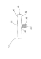
図面を参照しながら、本発明によるCVD及びエッチング環境中で利用される多数領域加熱システムの好ましい実施例を説明し、図1において一般的に符号10で示す。加熱システム10は、半導体ウェハー(図示されていない)の表面に渡って一様で一定な温度を維持し、CVD及びエッチング環境中での腐食性のガスから前記加熱素子の電気部品を保護する手段を提供する。
With reference to the drawings, a preferred embodiment of a multi-zone heating system utilized in a CVD and etch environment according to the present invention will be described and is generally designated 10 in FIG. The
図1から図6を参照すると、セラミックヒータ12は、中空軸18に取り付けられた一般的に平円盤状形態のセラミック体16を含む。セラミック体16は、一連の導電性の複合材料からなるセラミック層26,28,30,32,34及び36から構成されるセラミック基板から製造される。前記導電性の複合材料は、マイクロプロセッサー14によって、1つ又はそれ以上の加熱素子44と適切に作動する関係にある少なくとも1つの温度センサ38と共に、セラミック基板中に完全に及び直接的に埋め込まれている少なくとも2つ以上の加熱素子44を有している。セラミック層26,28,30,32,34及び36は、より詳細に後述されるセラミックヒータ12のセラミック基板中に完全に及び直接的に、複数の加熱素子44と複数のセンサ38とが埋め込まれたセラミック体16を形成する製造中に薄板を積層し焼結される。
Referring to FIGS. 1-6, the
図1を参照すると、複数の加熱素子44は、マイクロプロセッサー14によって作動制御される。複数の温度センサ38が、前記ヒータの一つの領域が、半導体ウェハー中の温度降下により低すぎたり、温度変動が発生し熱すぎたりすることを検知すると、前記半導体ウェハーの全表面に渡って一様な温度分布にし、これを維持するように、前記マイクロプロセッサー14は特定の複数の加熱素子44のパワーの増減を行う。
Referring to FIG. 1, the plurality of
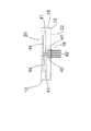
図4に示されるように、前記半導体ウェハーの全表面に渡って一様な温度を維持することは、セラミック体16のセラミック層28に沿って、分離した加熱領域28Aと加熱領域28Bに前記複数の加熱素子を分類することで達成される。製造中に、セラミック体16全体を形成する個々のセラミック層上に、複数の加熱素子44と複数の温度センサ38を適用することで、複数の加熱素子44と複数の温度センサ38は前記セラミック基板中に完全に埋め込まれる。
As shown in FIG. 4, maintaining a uniform temperature across the entire surface of the semiconductor wafer can be achieved by separating the plurality of
図6を参照すると、前記セラミック体は、製造中に薄板を積層し焼結される複数のセラミック層26,28,30,32,34及び36から構成されている。セラミックヒータ12を構成するために、幾つのセラミック層が利用されても、本発明の範疇に入ることに注意すべきである。好ましい具体例においては、複数の加熱素子44と複数の温度センサ38とを有するセラミック層28とセラミック層32を製造するために厚手のテープが用いられ、前記セラミック層28,32は、他の厚いテープから成るセラミック層26,30,34,36間に挟まれている。セラミック層26,30,34,36を製造するために用いられているテープは窒化アルミニウムから構成されている。一方、セラミック層28,32のテープもまた同一の窒化アルミニウムから形成されているが、それぞれ加熱素子44と温度センサ38のベースを形成するために用いられている。さらに、セラミック層28は、好ましくはモリブデンと窒化アルミニウムの複合体から構成された少なくとも二つの分離した加熱領域28A,28Bを形成するために厚手のテープの窒化アルミニウムを重ね継いだ追加の複合材料を含んでいる。さらに、セラミック層32は、温度センサ38を形成する前記セラミック層32の表面に直接重ね継がれているモリブデンと窒化アルミニウムを含んでいる。
Referring to FIG. 6, the ceramic body is composed of a plurality of
上述したように、セラミック層28は、窒化アルミニウム複合体から形成されたテープと共に加熱素子44として作用するモリブデンと窒化アルミニウムの複合体を重ね継ぐことで作成された多数領域の加熱素子配置を形成する。好ましくは、複合材料中のモリブデンの窒化アルミニウムに対する重量パーセント比はモリブデン20%〜55%、窒化アルミニウム80%〜45%の範囲である。この加熱素子の複合体は、少なくとも2つの分離した加熱素子44を提供するために前記複合テープから切り出され、分離した加熱領域を形成するために窒化アルミニウムから作成された前記テープに重ね継がれる。図4に示されるように、セラミック層28のテープとして予め形成された切り抜きの重ね継ぎは、二つの分離した加熱領域28A,28Bに分割された層28となる。各加熱領域28A,28Bは、少なくとも一つの分離し別個の、半導体ウェハーの表面に沿って一様な温度を提供し維持するために作動される加熱素子44を含んでいる。
As described above, the
本発明者らは、また、モリブデンと窒化アルミニウムの複合体からなる加熱素子44の構造が、0.00435/℃と高いTCRをもつモリブデンのような耐熱性金属からなる加熱素子44よりも低いTCR(即ち、0.0015/℃)を有する加熱素子44を可能にすることを発見した。モリブデンと窒化アルミニウムの複合体から形成された加熱素子44のこのより低いTCRは、前記セラミックヒータ12が立ち上がり時に最初に活性化された時に、低い「急襲する(rush in)」電流を生み出し、それによって作動エネルギー効率がより上がることになる。
The present inventors also have a structure in which the
上述し、図5に示されるように、複数の加熱素子44は、少なくとも1つのセラミック層32に沿って配置されている温度センサ38と個々に作動的に関連付けられている。セラミック層32は、セラミック層26,30,34,36に利用されている窒化アルミニウムの複合体と同様の材料から構成されているが、複数の温度センサ38を形成する製造中に、モリブデンと窒化アルミニウムの複合体のインクが前記窒化アルミニウムのテープ層の表面に適用される点は相違する。複数の温度センサ38中のモリブデンの比率は20%〜100%であり、残余が窒化アルミニウムであって良い。上述したように、もっとも好ましくは、このモリブデンと窒化アルミニウムの複合体は、当業者に利用されている方法であるセラミック層32のテープ表面に直接適用される液体インク混合物の形態である。それ故に、前記インクが最初にセラミック層32のテープに適用された時、前記インクは前記窒化アルミニウムテープの小さな部位に浸透し、温度センサ38を形成するモリブデンと窒化アルミニウムの複合体全体に、前記インク中の窒化アルミニウムの割合が増加する。したがって、たとえ最初にモリブデン100%が適用されても、前記温度センサは、テープから浸透した窒化アルミニウムに由来する少しの割合の窒化アルミニウムを含んでいる。
As described above and shown in FIG. 5, the plurality of
図3を参照すると、温度センサ38と加熱素子44は、それぞれ伝導路40,41で結合されている。好ましくは、伝導路40,41は、セラミックヒータ12の各加熱素子44と温度センサ38のための中空軸18に隣接して終わっているセラミック体16を掘り抜かれた軸方向路によって形成されている。前記軸方向伝導路40,41は、モリブデンと窒化アルミニウムの複合体から製造された伝導材料のスラグあるいは粉末で奥へ完全に満たされている。好ましくは、前記伝導材料は、加熱素子44の構成で用いられているモリブデンと窒化アルミニウムの比率と等しい比率であるモリブデンと窒化アルミニウムの比率を有している。
Referring to FIG. 3, the
前記伝導路40,41の各々はその終点で一対の導線42と結合されており、前記導線はマイクロプロセッサー14と動力源(図示せず)と作動的に関連付けられている。好ましくは、マイクロプロセッサー14は、温度センサ38からの複数の信号を受け取る手段を提供し、前記手段は、予め決められた抵抗対温度の較正曲線に基づいて温度示度に変換され、前記半導体ウェハーに沿って一定で一様な温度を維持するために、加熱領域28A,28Bをもつ個々の加熱素子44に付与される電力を自動的に調整する。
Each of the
上述したように、セラミックヒータ12は、各セラミック層26,28,30,32,34及び36用のテープの製作、及び複数の加熱素子44及び複数の温度センサ38をそれぞれ含むようにセラミック層28、32を改変することによって製造される。セラミック層26,28,30,32,34及び36用のテープを最初に構成する工程は、各テープとも類似している。窒化アルミニウムの粉末を有機結合剤とアクリル酸とトルエンのような溶媒とをスラリーにするために混合する。前記スラリーは、前記スラリーが乾燥しテープを形成するのを可能にするプラスチック担体上にドクターブレードによって適当な形に配列される。
As described above, the
さらに上述したように、セラミック層28は、加熱素子44を形成するために切断されてから互いに重ね継ぎされた二つの分離したテープから製造される。第1のテープは、セラミック層26,30,32,34及び36を製造するのに用いられたテープと同一の方法で製造された窒化アルミニウムを含んでいる。第2のテープは、モリブデンと窒化アルミニウムの複合体から製造され、前記セラミック層28の加熱素子部分として役立つ。モリブデンの重量パーセント比は20%〜45%で、複合体の残余部は窒化アルミニウムを含んでいる。一旦、セラミックヒータ28として2つのテープが製作されたなら、それらは1つの連続したテープを形成するために互いに重ね継ぎされる。セラミック層28のテープ内で今や重ね継ぎされた前記加熱素子部分は、2つ又はそれ以上の、分離した別個のセラミックヒータ12の加熱素子44を形成するモリブデンと窒化アルミニウムの複合体から製造された加熱領域を含んでいる。好ましくは、少なくとも2つの別個の加熱素子44が、少なくとも2つの個別に制御される加熱領域28A,28Bが可能となるようにテープ中に重ね継ぎされるが、本発明は2つ以上の加熱領域も制作され得ることを企図している。
As further described above, the
前記重ね継ぎ工程は、前記テープから窒化アルミニウムの一区画部分を取り去り、それを、加熱素子44として役立つ導電性のモリブデンと窒化アルミニウムの複合体を含んだテープから切り取られた同一の一区画部分と置き換えることによって達成される。好ましくは、各個別のテープはレーザー、ダイカット、又は当業者に知られた他の方法で切ると良い。2つのテープが切られた後は、各区画部分は他方に対して逆の形状を有するべきである。図4に示されるように、好ましい実施例においては、形状は一般的に円形であるが、角張った形状、正方形又は以上の組み合わせのような如何なる適切な輪郭でも本発明の範囲に入ると考えられる。前記区画部分が共に重ね継ぎされると、セラミックヒータ12の基板内に埋め込まれた複数の加熱素子44を伴ったセラミック層28のために、各々は平面で連続したテープを形成するように互いに結合する。図7を参照すると、本発明により製造された複数の加熱素子44は、先行技術の在来の耐熱性金属から構成された複数の加熱素子に見られるよりも非常に低いTCRを有している。例えば、モリブデンだけから構成された加熱素子は、図7に示されるように0.00435/℃のTCRを有するが、本発明によるモリブデンと窒化アルミニウムの複合体から製造された複数の加熱素子44は先行技術の機器より重要で低い0.0001/℃のTCRを有する。
The piecing step removes a section of aluminum nitride from the tape and replaces it with the same section cut from a tape containing a composite of conductive molybdenum and aluminum nitride that serves as the
セラミック層32に適用される複数の前記温度センサ38は、窒化アルミニウムと結合したモリブデンの液体混合物のインクから形成されている。前記モリブデンと窒化アルミニウムのインクはセラミック層32のテープ上に特別なパターンで付与され、乾燥されることで、少なくとも2つの温度センサ38が生成される。好ましい実施例においては、後に詳細に説明するが、各温度センサ38は少なくとも一つの個別の加熱素子44とマイクロプロセッサー14を通して作動的に関連しているので、多数の温度センサ38は、少なくとも多数の加熱領域に匹敵する。図8を参照すると、好ましくは、複数の温度センサ38は、温度に依存した抵抗のレベルを表現する抵抗温度検出(RTD)機器である。
The plurality of
一旦、セラミック層32のテープが、そのテープに付与されたモリブデンと窒化アルミニウムのインクを有し、セラミック層28のテープが、そのテープ中に重ね継がれた加熱素子44を備えて製造されたら、次の工程は、セラミック層26,28,30,32,34及び36の複数のテープを一体のセラミック体16を形成するために組み立てることである。
Once the
図6を参照すると、セラミック層26,28,30,32,34及び36の複数のテープは、各テープを順番に1つのテープを他のテープの上に積み重ねることで組み立てられる。複数のテープが適切に積み重ねられた後に、図3に示すように、電力を提供し、複数の前記加熱素子44と温度センサ38間の作動的な関連をマイクロプロセッサー14を通して可能とするために、伝導路40,41が各々加熱素子44と温度センサ38のために形成される。各加熱素子44のために、伝導路40は、セラミック層26とセラミック層28のテープを貫通して穴を設けることによって形成される。前記穴が形成された後、この穴は、加熱素子44に用いられる複合体と類似のモリブデンと窒化アルミニウム複合体から形成された詰め物又は粉末のいずれかで奥まで満たされる。この奥まで満たされた材料は加熱素子44と導線42とを連結する伝導路40を形成する。同様に、各温度センサ38のために、伝導路41がセラミック層26,28,30,32のテープを貫通して穴を設けることにより形成される。この穴もまた、モリブデンと窒化アルミニウム複合体材料で奥まで満たされ、各温度センサ38と導線42間で伝導路が確立される。伝導路40,41を形成する複合体のモリブデンと窒化アルミニウムの比率は、本発明の好ましい実施例の加熱素子44を形成するのに使用される比率と等しくあるべきである。
Referring to FIG. 6, a plurality of tapes of
適切な多数の伝導路40,41が生成された後、セラミック層26,28,30,32,34及び36の前記テープは、セラミック体16を生成するために積み重ねて焼結される。積層は、従来の鋳型内に積み重ねられた全てのテープを配置し、前記複数のテープの表面に従来の積層形成技術を適用することで完遂される。次に、セラミック層26,28,30,32,34及び36は共に、温度範囲1700〜1900℃、圧力100〜3000psiで焼結される。特定の範囲を示したが、セラミック基板を形成するために効果的に複数のテープを共に焼結する如何なる温度と圧力の範囲も、本発明の範囲に入るであろう。熱間静水圧圧縮成形のような平板を共に焼結する如何なる既知の手段をも利用することができ、それでもやはり本発明の範囲に入る。
After the appropriate number of
焼結工程が完成後、好ましくはニッケルから構成される複数の導線42が各伝導路40,41にロウ付けされ、そして当業者に良く知られた手段でセラミック体16に取り付けられた中空軸18を通して給電される。それから前記複数の導線42の自由端は、マイクロプロセッサー14と動力源と同様に複数の加熱素子44と複数の温度センサ38とを作動的に関連付けているマイクロプロセッサー14に結合される。
After the sintering process is complete, a plurality of
操作においては、セラミック体16の全ての部分にわたって埋め込まれている複数の加熱素子44と複数の温度センサ38による多数領域の加熱配置によって、加熱システム10は半導体ウェハーの表面に渡って一定で一様な温度を提供することができる。最初に半導体ウェハーがセラミックヒータ12上に置かれた時に、前記半導体ウェハーの一部分だけへの冷却ガスの影響によって、前記ウェハーの複数のある一定の部分が他の部分よりも冷たくなる。
In operation, the
前記半導体ウェハーの前記表面に渡ってのこの温度変動を修正するために、マイクロプロセッサー14が、抵抗の信号を温度示度信号に変換する較正曲線を用いて特に設計されたウェハー(図示せず)を通して、種々の温度センサ38からの温度示度を受け取る。それから、前記温度センサ38は、導線42からの信号を領域28A(又は28B)に配置された個々の加熱素子44に送る。それから個々の加熱素子44はマイクロプロセッサー14によってその電力が調整され、その結果、他の加熱領域に付与される熱よりも、多くの熱が特定の加熱領域に付与される。この付加的な加熱が、前記半導体ウェハーの冷却ガスの影響で冷たすぎる前記領域を暖める。その特定の加熱領域への付加的な熱は、両方の加熱領域28A,28Bから伝達される温度示度が等しくなるまで継続される。この加熱領域28Aと加熱領域28B間の温度の平衡を保つことで、前記半導体ウェハーの全表面が一定の温度に留まるだろう。さらに、複数の加熱素子44及び温度センサ38が、完全に直接セラミック体16のセラミック基板に埋め込まれているので、それらはCVD及びエッチング環境の腐食環境に曝されないであろう。
To correct for this temperature variation across the surface of the semiconductor wafer, the
本発明の特別な具体例が図解され記述されたが、上述のものから、本発明の精神と範囲から離れることなく、それに対して種々の変形が可能である。それ故に、本発明は本明細書に限定されることなく、本発明の範囲は添付した特許請求の範囲だけに限定されることを意図している。 While particular embodiments of the present invention have been illustrated and described, various modifications can be made thereto without departing from the spirit and scope of the present invention. Therefore, it is intended that the invention not be limited to the present specification, but that the scope of the invention be limited only to the appended claims.
Claims (35)
(a)多数のテープの層からなる多数のセラミック層を備えたセラミック基板と、
(b)前記セラミック基板内部に直接埋め込まれた加熱素子配置であって、前記多数のセラミック層の一つに重ね継がれた複合テープを備えた加熱素子配置と、
(c)前記加熱素子配置と作動的に関連付けられた温度センサ配置であって、前記セラミック基板内部に完全に埋め込まれている温度センサ配置と、
を備え、
前記温度センサ配置を前記セラミック基板内部に完全に埋め込むために、前記セラミック基板及び前記温度センサ配置は、互いに浸透させられているセラミックヒータ。A ceramic heater,
(A) a ceramic substrate comprising a number of ceramic layers comprising a number of tape layers ;
(B) a heating element arrangement directly embedded inside the ceramic substrate, the heating element arrangement comprising a composite tape layered over one of the multiple ceramic layers ;
(C) a temperature sensor arrangement operatively associated with the heating element arrangement, wherein the temperature sensor arrangement is completely embedded within the ceramic substrate;
With
In order to completely embed the temperature sensor arrangement inside the ceramic substrate, the ceramic substrate and the temperature sensor arrangement are infiltrated with each other.
(a)多数のテープの層からなる多数のセラミック層と、
(b)前記多数のセラミック層内部に直接埋め込まれ、少なくとも2つの個別で別個の加熱領域を形成する加熱素子配置であって、前記多数のセラミック層の一つに重ね継がれた複合テープを備えた加熱素子配置と、
(c)前記多数のセラミック層内部に完全に埋め込まれ、前記加熱素子配置と作動的に関連付けられている温度センサ配置と、
を備え、
前記多数のセラミック層と前記温度センサ配置は、互いに浸透させられているセラミックヒータ。A ceramic heater,
(A) a number of ceramic layers consisting of a number of tape layers;
(B) a heating element arrangement that is directly embedded within the multiple ceramic layers to form at least two separate and distinct heating zones , comprising a composite tape overlaid on one of the multiple ceramic layers a heating element arrangement has,
(C) a temperature sensor arrangement fully embedded within the multiple ceramic layers and operatively associated with the heating element arrangement;
With
The ceramic heater in which the plurality of ceramic layers and the temperature sensor arrangement are infiltrated with each other.
(a)セラミックヒータは、
(i)セラミック基板を形成する多数のテープの層からなる多数のセラミック層と、
(ii)前記多数のセラミック層の内部に直接埋め込まれた加熱素子配置であって、前記多数のセラミック層の一つに重ね継がれた複合テープを備えた加熱素子配置と、
(iii)前記多数のセラミック層の内部に直接埋め込まれた温度センサ配置であって、前記加熱素子配置と作動的に関連付けられた温度センサ配置と、
を備え、
(b)マイクロプロセッサーが、前記半導体ウェハーの表面に渡って一様な温度分布を維持するために、前記加熱素子配置と前記温度検出配置とに作動的に関連付けられており、
前記温度センサ配置を前記多数の前記セラミック層内部に完全に埋め込むために、前記多数のセラミック層と前記温度センサ配置は、互いに浸透させられている加熱システム。A heating system for maintaining a uniform temperature across a semiconductor wafer,
(A) Ceramic heater
(I) a number of ceramic layers comprising a number of tape layers forming a ceramic substrate;
(Ii) a heating element arrangement embedded directly within the multiple ceramic layers, the heating element arrangement comprising a composite tape overlaid on one of the multiple ceramic layers ;
(Iii) a temperature sensor arrangement directly embedded within the multiple ceramic layers, wherein the temperature sensor arrangement is operatively associated with the heating element arrangement;
Bei to give a,
(B) microprocessor, said in order to maintain a uniform temperature distribution across the surface of the semiconductor wafer, Ri Contact operatively associated with the said temperature sensing arrangement and said heating element arrangement,
A heating system in which the multiple ceramic layers and the temperature sensor arrangement are infiltrated with each other to completely embed the temperature sensor arrangement within the multiple ceramic layers.
(a)(i)多数のテープの層からなる多数のセラミック層と、
(ii)前記多数のセラミック層の内部に直接埋め込まれた加熱素子配置であって、前記加熱素子配置は少なくとも2つの独立した別個の加熱領域を形成しており、前記加熱素子配置は前記多数のセラミック層の一つに重ね継がれた複合テープを備え、
(iii)前記多数のセラミック層の内部に完全に埋め込まれた温度センサであって、前記温度センサは分離して、前記加熱素子配置と作動的に関連付けられており、前記温度センサを前記セラミック層内部に完全に埋め込むために、複数の前記セラミック層及び温度センサは、互いに浸透させられていることと、
を備えたセラミックヒータ準備する工程と、
(b)前記物体を前記セラミックヒータと伝達するように配置する工程と、
(c)前記物体の表面に渡って異なっている温度を検出する前記温度センサを可能ならしめる工程と、
(d)前記物体に渡っての前記異なっている温度を除去するために前記加熱素子配置を調整する工程と、
を備えた物体に一定で一様な熱源を付与する方法。A method of applying a constant and uniform heat source to an object,
(A) (i) a number of ceramic layers comprising a number of tape layers;
(Ii) a heating element arrangement embedded directly within the multiple ceramic layers, wherein the heating element arrangement forms at least two separate and distinct heating regions, the heating element arrangement being It is equipped with a composite tape that is superposed on one of the ceramic layers.
(Iii) a temperature sensor fully embedded within the plurality of ceramic layers, wherein the temperature sensor is separate and operatively associated with the heating element arrangement, the temperature sensor being connected to the ceramic layer; A plurality of said ceramic layers and temperature sensors are infiltrated with each other in order to be completely embedded inside;
Preparing a ceramic heater comprising:
(B) arranging the object to communicate with the ceramic heater;
(C) enabling the temperature sensor to detect different temperatures across the surface of the object;
(D) adjusting the heating element arrangement to remove the different temperatures across the object;
A method for applying a constant and uniform heat source to an object provided with
(a)多数のテープの層を準備する工程と、
(b)前記多数のテープの層の1つの内部に、複合テープを備えた加熱素子配置を配置し、前記多数のテープの層の一つに前記複合テープを重ね継ぐ工程と、
(c)前記多数のテープの層の1つに前記加熱素子配置から分離している温度センサを適用する工程と、
(d)前記多数のテープの層を共に配置する工程と、
(e)前記多数のテープの層からセラミック複合体を形成する工程であって、前記加熱素子配置と前記温度センサは、一工程で前記セラミックヒータ内に焼結され、前記加熱素子配置と前記温度センサとが完全に前記セラミック複合体内部に埋め込まれる前記多数のテープの層からセラミック複合体を形成する工程と、
を備えたセラミックヒータを製造する方法。A method of manufacturing a ceramic heater for heating a semiconductor wafer in a chemical vapor deposition method and an etching environment,
(A) preparing a number of tape layers;
(B) disposing a heating element arrangement comprising a composite tape inside one of the multiple tape layers, and superimposing the composite tape on one of the multiple tape layers ;
(C) applying a temperature sensor separated from the heating element arrangement to one of the plurality of tape layers;
(D) arranging the multiple tape layers together;
(E) forming a ceramic composite from the layers of the plurality of tapes, wherein the heating element arrangement and the temperature sensor are sintered in the ceramic heater in one step, and the heating element arrangement and the temperature Forming a ceramic composite from the multiple layers of tape, wherein a sensor is completely embedded within the ceramic composite;
A method of manufacturing a ceramic heater comprising:
Applications Claiming Priority (3)
| Application Number | Priority Date | Filing Date | Title |
|---|---|---|---|
| US10/431,758 US20040222210A1 (en) | 2003-05-08 | 2003-05-08 | Multi-zone ceramic heating system and method of manufacture thereof |
| US10/431,758 | 2003-05-08 | ||
| PCT/US2004/004251 WO2004102076A2 (en) | 2003-05-08 | 2004-02-13 | Multi-zone ceramic heating system and method of manufacture thereof |
Publications (2)
| Publication Number | Publication Date |
|---|---|
| JP2007515778A JP2007515778A (en) | 2007-06-14 |
| JP4908217B2 true JP4908217B2 (en) | 2012-04-04 |
Family
ID=33416519
Family Applications (1)
| Application Number | Title | Priority Date | Filing Date |
|---|---|---|---|
| JP2006532286A Expired - Lifetime JP4908217B2 (en) | 2003-05-08 | 2004-02-13 | Multi-region ceramic heating system and method of manufacturing the same |
Country Status (6)
| Country | Link |
|---|---|
| US (1) | US20040222210A1 (en) |
| EP (1) | EP1621048B1 (en) |
| JP (1) | JP4908217B2 (en) |
| AT (1) | ATE410905T1 (en) |
| DE (1) | DE602004016985D1 (en) |
| WO (1) | WO2004102076A2 (en) |
Families Citing this family (20)
| Publication number | Priority date | Publication date | Assignee | Title |
|---|---|---|---|---|
| US8206996B2 (en) | 2006-03-28 | 2012-06-26 | Lam Research Corporation | Etch tool process indicator method and apparatus |
| US7951616B2 (en) * | 2006-03-28 | 2011-05-31 | Lam Research Corporation | Process for wafer temperature verification in etch tools |
| US7572480B2 (en) * | 2006-10-19 | 2009-08-11 | Federal-Mogul World Wide, Inc. | Method of fabricating a multilayer ceramic heating element |
| JP4879060B2 (en) * | 2007-03-26 | 2012-02-15 | 日本碍子株式会社 | Substrate heating device |
| US8637794B2 (en) | 2009-10-21 | 2014-01-28 | Lam Research Corporation | Heating plate with planar heating zones for semiconductor processing |
| US8791392B2 (en) | 2010-10-22 | 2014-07-29 | Lam Research Corporation | Methods of fault detection for multiplexed heater array |
| US8546732B2 (en) * | 2010-11-10 | 2013-10-01 | Lam Research Corporation | Heating plate with planar heater zones for semiconductor processing |
| WO2013130593A1 (en) * | 2012-02-27 | 2013-09-06 | Watlow Electric Manufacturing Company | Temperature detection and control system for layered heaters |
| DE102012101717A1 (en) * | 2012-03-01 | 2013-09-05 | Aixtron Se | Method and device for controlling the surface temperature of a susceptor of a substrate coating device |
| US9224626B2 (en) * | 2012-07-03 | 2015-12-29 | Watlow Electric Manufacturing Company | Composite substrate for layered heaters |
| DE102012111458B4 (en) * | 2012-11-27 | 2022-12-08 | Tdk Electronics Ag | semiconductor device |
| CN104131268B (en) * | 2013-05-03 | 2017-02-08 | 北京北方微电子基地设备工艺研究中心有限责任公司 | Divisionally heating method, divisionally heating apparatus and semi-conductor device |
| JP6084906B2 (en) * | 2013-07-11 | 2017-02-22 | 日本碍子株式会社 | Ceramic heater |
| CN103874243B (en) * | 2014-03-27 | 2016-06-01 | 福建闽航电子有限公司 | The ceramic heating plate of a kind of band temperature control |
| KR20180112794A (en) * | 2016-01-22 | 2018-10-12 | 어플라이드 머티어리얼스, 인코포레이티드 | Ceramic shower head with conductive layers embedded |
| JP6758143B2 (en) * | 2016-09-29 | 2020-09-23 | 日本特殊陶業株式会社 | Heating device |
| US10679873B2 (en) * | 2016-09-30 | 2020-06-09 | Ngk Spark Plug Co., Ltd. | Ceramic heater |
| US10796935B2 (en) * | 2017-03-17 | 2020-10-06 | Applied Materials, Inc. | Electronic device manufacturing systems, methods, and apparatus for heating substrates and reducing contamination in loadlocks |
| GB2562075B (en) * | 2017-05-03 | 2022-03-16 | Jemella Ltd | Barrel for hair styling appliance |
| WO2021108176A1 (en) * | 2019-11-26 | 2021-06-03 | Tokyo Electron Limited | THERMAL TREATMENTS USING A PLURALITY OF EMBEDDED RESISTANCE TEMPERATURE DETECTORS (RTDs) |
Citations (6)
| Publication number | Priority date | Publication date | Assignee | Title |
|---|---|---|---|---|
| JPH0478138A (en) * | 1990-07-20 | 1992-03-12 | Ngk Insulators Ltd | Semiconductor wafer heating device and its manufacture |
| JPH08274147A (en) * | 1995-03-30 | 1996-10-18 | Kyocera Corp | Wafer holding device |
| JPH11214127A (en) * | 1998-01-21 | 1999-08-06 | Riken Corp | Heater device and manufacture of the same |
| JP2000236015A (en) * | 1999-02-16 | 2000-08-29 | Toshiba Corp | Manufacture of hot plate and semiconductor device |
| JP2001217059A (en) * | 2000-02-03 | 2001-08-10 | Ngk Insulators Ltd | Heating device |
| WO2002084717A1 (en) * | 2001-04-11 | 2002-10-24 | Ibiden Co., Ltd. | Ceramic heater for semiconductor manufactring/inspecting apparatus |
Family Cites Families (46)
| Publication number | Priority date | Publication date | Assignee | Title |
|---|---|---|---|---|
| US134775A (en) * | 1873-01-14 | Improvement in transplanters | ||
| US166854A (en) * | 1875-08-17 | Improvement in vehicle fifth-wheels | ||
| US2938103A (en) * | 1958-04-11 | 1960-05-24 | Electrofilm Inc | Thermostat-carrying electrical heating materials for surface application |
| US3789190A (en) * | 1972-10-17 | 1974-01-29 | A J Matlen | Temperature regulation for electrical heater |
| US3813520A (en) * | 1973-03-28 | 1974-05-28 | Corning Glass Works | Electric heating unit |
| US4549073A (en) * | 1981-11-06 | 1985-10-22 | Oximetrix, Inc. | Current controller for resistive heating element |
| JPH0719645B2 (en) * | 1984-09-07 | 1995-03-06 | 日本電装株式会社 | Self-temperature controlled heating device |
| JPS6183825A (en) * | 1984-10-02 | 1986-04-28 | Babcock Hitachi Kk | Ignition device of burner |
| GB8514785D0 (en) * | 1985-06-11 | 1985-07-10 | Micropore International Ltd | Infra-red heaters |
| US4640224A (en) * | 1985-08-05 | 1987-02-03 | Spectrum Cvd, Inc. | CVD heat source |
| US4607591A (en) * | 1985-08-06 | 1986-08-26 | Spectrum Cvd, Inc. | CVD heater control circuit |
| JPH0617272B2 (en) * | 1986-02-12 | 1994-03-09 | 株式会社日本自動車部品総合研究所 | Silicon nitride-alumina composite ceramics and method for producing the same |
| US4778559A (en) * | 1986-10-15 | 1988-10-18 | Advantage Production Technology | Semiconductor substrate heater and reactor process and apparatus |
| US4937435A (en) * | 1987-12-14 | 1990-06-26 | Thermon Manufacturing Company | Flexible electric heating pad using PTC ceramic thermistor chip heating elements |
| US5001423A (en) * | 1990-01-24 | 1991-03-19 | International Business Machines Corporation | Dry interface thermal chuck temperature control system for semiconductor wafer testing |
| US5134248A (en) * | 1990-08-15 | 1992-07-28 | Advanced Temperature Devices, Inc. | Thin film flexible electrical connector |
| GB9020400D0 (en) * | 1990-09-19 | 1990-10-31 | Raychem Sa Nv | Electrical heating tape |
| DE69130205T2 (en) * | 1990-12-25 | 1999-03-25 | Ngk Insulators Ltd | Semiconductor wafer heater and method of manufacturing the same |
| US5264681A (en) * | 1991-02-14 | 1993-11-23 | Ngk Spark Plug Co., Ltd. | Ceramic heater |
| US5436172A (en) * | 1991-05-20 | 1995-07-25 | Texas Instruments Incorporated | Real-time multi-zone semiconductor wafer temperature and process uniformity control system |
| DE4130337C2 (en) * | 1991-09-12 | 2002-05-02 | Ego Elektro Blanc & Fischer | Method for operating an electric heating unit and electric heating unit |
| FR2682253A1 (en) * | 1991-10-07 | 1993-04-09 | Commissariat Energie Atomique | HEATING SOLE FOR PROVIDING THE HEATING OF AN OBJECT PROVIDED ON ITS SURFACE AND CHEMICAL PROCESSING REACTOR PROVIDED WITH SAID SOLE. |
| US5268989A (en) * | 1992-04-16 | 1993-12-07 | Texas Instruments Incorporated | Multi zone illuminator with embeded process control sensors and light interference elimination circuit |
| US5783805A (en) * | 1992-06-05 | 1998-07-21 | Katzmann; Fred L. | Electrothermal conversion elements, apparatus and methods for use in comparing, calibrating and measuring electrical signals |
| JP2828575B2 (en) * | 1993-11-12 | 1998-11-25 | 京セラ株式会社 | Silicon nitride ceramic heater |
| US6133557A (en) * | 1995-01-31 | 2000-10-17 | Kyocera Corporation | Wafer holding member |
| US5715361A (en) * | 1995-04-13 | 1998-02-03 | Cvc Products, Inc. | Rapid thermal processing high-performance multizone illuminator for wafer backside heating |
| US5830277A (en) * | 1995-05-26 | 1998-11-03 | Mattson Technology, Inc. | Thermal processing system with supplemental resistive heater and shielded optical pyrometry |
| US5881208A (en) * | 1995-12-20 | 1999-03-09 | Sematech, Inc. | Heater and temperature sensor array for rapid thermal processing thermal core |
| EP0899986B1 (en) * | 1996-05-05 | 2004-11-24 | Tateho Chemical Industries Co., Ltd. | Electric heating element and electrostatic chuck using the same |
| US5885353A (en) * | 1996-06-21 | 1999-03-23 | Micron Technology, Inc. | Thermal conditioning apparatus |
| US6066836A (en) * | 1996-09-23 | 2000-05-23 | Applied Materials, Inc. | High temperature resistive heater for a process chamber |
| KR100551980B1 (en) * | 1997-11-03 | 2006-02-20 | 에이에스엠 아메리카, 인코포레이티드 | Method and Apparatus of Processing Wafers with Low Mass Support |
| US5970214A (en) * | 1998-05-14 | 1999-10-19 | Ag Associates | Heating device for semiconductor wafers |
| JP2000058237A (en) * | 1998-06-05 | 2000-02-25 | Ngk Spark Plug Co Ltd | Ceramic heater and oxygen sensor using it |
| JP3764278B2 (en) * | 1998-07-13 | 2006-04-05 | 株式会社東芝 | Substrate heating apparatus, substrate heating method, and substrate processing method |
| US6469283B1 (en) * | 1999-03-04 | 2002-10-22 | Applied Materials, Inc. | Method and apparatus for reducing thermal gradients within a substrate support |
| US6231933B1 (en) * | 1999-03-18 | 2001-05-15 | Primaxx, Inc. | Method and apparatus for metal oxide chemical vapor deposition on a substrate surface |
| US6191394B1 (en) * | 1999-05-19 | 2001-02-20 | Tokyo Electron Ltd. | Heat treating apparatus |
| JP3228923B2 (en) * | 2000-01-18 | 2001-11-12 | イビデン株式会社 | Ceramic heater for semiconductor manufacturing and inspection equipment |
| WO2001084888A1 (en) * | 2000-04-29 | 2001-11-08 | Ibiden Co., Ltd. | Ceramic heater and method of controlling temperature of the ceramic heater |
| CN100401852C (en) * | 2001-04-30 | 2008-07-09 | 科林研发公司 | Method and apparatus for controlling spatial temperature distribution across surface of workpiece support |
| DE10125350A1 (en) * | 2001-05-23 | 2002-11-28 | Linde Ag | Device for cooling a component using a hydraulic fluid from a hydraulic circulation comprises a component positioned in a suction line connecting a tank to a pump and a control valve arranged between the component and the pump |
| US6529686B2 (en) * | 2001-06-06 | 2003-03-04 | Fsi International, Inc. | Heating member for combination heating and chilling apparatus, and methods |
| JP3888531B2 (en) * | 2002-03-27 | 2007-03-07 | 日本碍子株式会社 | Ceramic heater, method for manufacturing ceramic heater, and buried article of metal member |
| JP4136696B2 (en) * | 2003-02-12 | 2008-08-20 | キヤノン株式会社 | Image forming apparatus and image forming method |
-
2003
- 2003-05-08 US US10/431,758 patent/US20040222210A1/en not_active Abandoned
-
2004
- 2004-02-13 AT AT04711141T patent/ATE410905T1/en not_active IP Right Cessation
- 2004-02-13 EP EP04711141A patent/EP1621048B1/en not_active Expired - Lifetime
- 2004-02-13 WO PCT/US2004/004251 patent/WO2004102076A2/en active Application Filing
- 2004-02-13 DE DE602004016985T patent/DE602004016985D1/en not_active Expired - Lifetime
- 2004-02-13 JP JP2006532286A patent/JP4908217B2/en not_active Expired - Lifetime
Patent Citations (6)
| Publication number | Priority date | Publication date | Assignee | Title |
|---|---|---|---|---|
| JPH0478138A (en) * | 1990-07-20 | 1992-03-12 | Ngk Insulators Ltd | Semiconductor wafer heating device and its manufacture |
| JPH08274147A (en) * | 1995-03-30 | 1996-10-18 | Kyocera Corp | Wafer holding device |
| JPH11214127A (en) * | 1998-01-21 | 1999-08-06 | Riken Corp | Heater device and manufacture of the same |
| JP2000236015A (en) * | 1999-02-16 | 2000-08-29 | Toshiba Corp | Manufacture of hot plate and semiconductor device |
| JP2001217059A (en) * | 2000-02-03 | 2001-08-10 | Ngk Insulators Ltd | Heating device |
| WO2002084717A1 (en) * | 2001-04-11 | 2002-10-24 | Ibiden Co., Ltd. | Ceramic heater for semiconductor manufactring/inspecting apparatus |
Also Published As
| Publication number | Publication date |
|---|---|
| EP1621048A2 (en) | 2006-02-01 |
| EP1621048A4 (en) | 2007-04-11 |
| EP1621048B1 (en) | 2008-10-08 |
| WO2004102076A2 (en) | 2004-11-25 |
| ATE410905T1 (en) | 2008-10-15 |
| DE602004016985D1 (en) | 2008-11-20 |
| JP2007515778A (en) | 2007-06-14 |
| WO2004102076A3 (en) | 2005-06-16 |
| US20040222210A1 (en) | 2004-11-11 |
Similar Documents
| Publication | Publication Date | Title |
|---|---|---|
| JP4908217B2 (en) | Multi-region ceramic heating system and method of manufacturing the same | |
| CN100538920C (en) | Stable pyrostat/heater system with tungsten/aluminium nitride | |
| KR101781032B1 (en) | Multi-zone resistive heating apparatus, reactor incorporating the multi-zone resistive heating apparatus, heating system for a chemical vapor deposition apparatus, and method for resistive heating of substrate | |
| US7473029B2 (en) | Thermoanalytical sensor, and method of producing the thermoanalytical sensor | |
| CN104769403B (en) | Hygrosensor and the method for manufacturing hygrosensor | |
| US6376811B2 (en) | Heating apparatus | |
| KR20140004758A (en) | Methods and apparatus for a multi-zone pedestal heater | |
| US20040206747A1 (en) | Ceramic heater for semiconductor manufacturing/inspecting apparatus | |
| CN105209872B (en) | Thermoelectric pile differential scanning calorimeter sensor | |
| EP1089593A2 (en) | Ceramic heater | |
| CN104931523B (en) | Thermoanalytic sensor and the method for manufacturing the sensor | |
| JP2007064865A (en) | Gas sensor and method of manufacturing gas sensor | |
| JP3677366B2 (en) | Ceramic heater | |
| JP4098112B2 (en) | Heater unit | |
| JP3515900B2 (en) | Ceramic heater | |
| JP2007085880A (en) | Thin thermocouple and manufacturing method therefor | |
| US7332694B2 (en) | Heating resistances and heaters | |
| JP2000286331A (en) | Wafer support member | |
| EP0334614A2 (en) | Catalytic gas detector | |
| JP2023170989A (en) | ceramic heater | |
| JPH0221675A (en) | Substrate for thin film thermopile use | |
| JPH07258837A (en) | Ceramic target with sensor | |
| CN115290214A (en) | In-situ wired wafer film temperature sensor | |
| JPH0369161B2 (en) | ||
| KR20020081847A (en) | apparatus for emitting heat |
Legal Events
| Date | Code | Title | Description |
|---|---|---|---|
| A977 | Report on retrieval |
Free format text: JAPANESE INTERMEDIATE CODE: A971007 Effective date: 20090311 |
|
| A131 | Notification of reasons for refusal |
Free format text: JAPANESE INTERMEDIATE CODE: A131 Effective date: 20090317 |
|
| A601 | Written request for extension of time |
Free format text: JAPANESE INTERMEDIATE CODE: A601 Effective date: 20090608 |
|
| A602 | Written permission of extension of time |
Free format text: JAPANESE INTERMEDIATE CODE: A602 Effective date: 20090615 |
|
| A521 | Request for written amendment filed |
Free format text: JAPANESE INTERMEDIATE CODE: A523 Effective date: 20090917 |
|
| A131 | Notification of reasons for refusal |
Free format text: JAPANESE INTERMEDIATE CODE: A131 Effective date: 20091208 |
|
| A601 | Written request for extension of time |
Free format text: JAPANESE INTERMEDIATE CODE: A601 Effective date: 20100308 |
|
| A602 | Written permission of extension of time |
Free format text: JAPANESE INTERMEDIATE CODE: A602 Effective date: 20100317 |
|
| A521 | Request for written amendment filed |
Free format text: JAPANESE INTERMEDIATE CODE: A523 Effective date: 20100607 |
|
| A131 | Notification of reasons for refusal |
Free format text: JAPANESE INTERMEDIATE CODE: A131 Effective date: 20110301 |
|
| TRDD | Decision of grant or rejection written | ||
| A01 | Written decision to grant a patent or to grant a registration (utility model) |
Free format text: JAPANESE INTERMEDIATE CODE: A01 Effective date: 20111213 |
|
| A01 | Written decision to grant a patent or to grant a registration (utility model) |
Free format text: JAPANESE INTERMEDIATE CODE: A01 |
|
| A61 | First payment of annual fees (during grant procedure) |
Free format text: JAPANESE INTERMEDIATE CODE: A61 Effective date: 20120112 |
|
| FPAY | Renewal fee payment (event date is renewal date of database) |
Free format text: PAYMENT UNTIL: 20150120 Year of fee payment: 3 |
|
| R150 | Certificate of patent or registration of utility model |
Ref document number: 4908217 Country of ref document: JP Free format text: JAPANESE INTERMEDIATE CODE: R150 Free format text: JAPANESE INTERMEDIATE CODE: R150 |
|
| R250 | Receipt of annual fees |
Free format text: JAPANESE INTERMEDIATE CODE: R250 |
|
| R250 | Receipt of annual fees |
Free format text: JAPANESE INTERMEDIATE CODE: R250 |
|
| R250 | Receipt of annual fees |
Free format text: JAPANESE INTERMEDIATE CODE: R250 |
|
| R250 | Receipt of annual fees |
Free format text: JAPANESE INTERMEDIATE CODE: R250 |
|
| R250 | Receipt of annual fees |
Free format text: JAPANESE INTERMEDIATE CODE: R250 |
|
| R250 | Receipt of annual fees |
Free format text: JAPANESE INTERMEDIATE CODE: R250 |
|
| R250 | Receipt of annual fees |
Free format text: JAPANESE INTERMEDIATE CODE: R250 |
|
| R250 | Receipt of annual fees |
Free format text: JAPANESE INTERMEDIATE CODE: R250 |
|
| R250 | Receipt of annual fees |
Free format text: JAPANESE INTERMEDIATE CODE: R250 |
|
| R250 | Receipt of annual fees |
Free format text: JAPANESE INTERMEDIATE CODE: R250 |
|
| EXPY | Cancellation because of completion of term |