JP4908006B2 - Semiconductor device - Google Patents
Semiconductor device Download PDFInfo
- Publication number
- JP4908006B2 JP4908006B2 JP2006026782A JP2006026782A JP4908006B2 JP 4908006 B2 JP4908006 B2 JP 4908006B2 JP 2006026782 A JP2006026782 A JP 2006026782A JP 2006026782 A JP2006026782 A JP 2006026782A JP 4908006 B2 JP4908006 B2 JP 4908006B2
- Authority
- JP
- Japan
- Prior art keywords
- comb
- wiring
- mos
- capacitor
- insulating film
- Prior art date
- Legal status (The legal status is an assumption and is not a legal conclusion. Google has not performed a legal analysis and makes no representation as to the accuracy of the status listed.)
- Expired - Fee Related
Links
Images


Classifications
-
- H—ELECTRICITY
- H10—SEMICONDUCTOR DEVICES; ELECTRIC SOLID-STATE DEVICES NOT OTHERWISE PROVIDED FOR
- H10D—INORGANIC ELECTRIC SEMICONDUCTOR DEVICES
- H10D1/00—Resistors, capacitors or inductors
- H10D1/60—Capacitors
- H10D1/62—Capacitors having potential barriers
- H10D1/66—Conductor-insulator-semiconductor capacitors, e.g. MOS capacitors
-
- H—ELECTRICITY
- H02—GENERATION; CONVERSION OR DISTRIBUTION OF ELECTRIC POWER
- H02M—APPARATUS FOR CONVERSION BETWEEN AC AND AC, BETWEEN AC AND DC, OR BETWEEN DC AND DC, AND FOR USE WITH MAINS OR SIMILAR POWER SUPPLY SYSTEMS; CONVERSION OF DC OR AC INPUT POWER INTO SURGE OUTPUT POWER; CONTROL OR REGULATION THEREOF
- H02M3/00—Conversion of DC power input into DC power output
- H02M3/02—Conversion of DC power input into DC power output without intermediate conversion into AC
- H02M3/04—Conversion of DC power input into DC power output without intermediate conversion into AC by static converters
- H02M3/06—Conversion of DC power input into DC power output without intermediate conversion into AC by static converters using resistors or capacitors, e.g. potential divider
- H02M3/07—Conversion of DC power input into DC power output without intermediate conversion into AC by static converters using resistors or capacitors, e.g. potential divider using capacitors charged and discharged alternately by semiconductor devices with control electrode, e.g. charge pumps
- H02M3/073—Charge pumps of the Schenkel-type
-
- H—ELECTRICITY
- H10—SEMICONDUCTOR DEVICES; ELECTRIC SOLID-STATE DEVICES NOT OTHERWISE PROVIDED FOR
- H10D—INORGANIC ELECTRIC SEMICONDUCTOR DEVICES
- H10D89/00—Aspects of integrated devices not covered by groups H10D84/00 - H10D88/00
- H10D89/211—Design considerations for internal polarisation
- H10D89/213—Design considerations for internal polarisation in field-effect devices
- H10D89/215—Design considerations for internal polarisation in field-effect devices comprising arrangements for charge pumping or biasing substrates
-
- H—ELECTRICITY
- H10—SEMICONDUCTOR DEVICES; ELECTRIC SOLID-STATE DEVICES NOT OTHERWISE PROVIDED FOR
- H10W—GENERIC PACKAGES, INTERCONNECTIONS, CONNECTORS OR OTHER CONSTRUCTIONAL DETAILS OF DEVICES COVERED BY CLASS H10
- H10W20/00—Interconnections in chips, wafers or substrates
- H10W20/40—Interconnections external to wafers or substrates, e.g. back-end-of-line [BEOL] metallisations or vias connecting to gate electrodes
- H10W20/495—Capacitive arrangements or effects of, or between wiring layers
- H10W20/496—Capacitor integral with wiring layers
Landscapes
- Engineering & Computer Science (AREA)
- Power Engineering (AREA)
- Semiconductor Integrated Circuits (AREA)
- Metal-Oxide And Bipolar Metal-Oxide Semiconductor Integrated Circuits (AREA)
Description
本発明は、半導体基板上に形成されるMOSキャパシタを備えた半導体装置に関するものである。 The present invention relates to a semiconductor device including a MOS capacitor formed on a semiconductor substrate.
従来、半導体基板上に形成されるキャパシタ素子には、MOSキャパシタやPIP(Poly-Insulator-Poly)キャパシタ、MIM(Metal-Insulator-Metal)キャパシタ等がある。これらのうちPIPキャパシタやMIMキャパシタは、電極間に挟まれる誘電体層に、より誘電率の高い材料が使用される。したがって、製造プロセスが増加したり、プロセスコストが高くなったりする場合がある。このためCMOSプロセスで作成する回路には、他のMOSトランジスタと整合させることを考えて、MOSキャパシタを使用することが多い。 Conventionally, capacitor elements formed on a semiconductor substrate include MOS capacitors, PIP (Poly-Insulator-Poly) capacitors, MIM (Metal-Insulator-Metal) capacitors, and the like. Among these, PIP capacitors and MIM capacitors use a material having a higher dielectric constant for the dielectric layer sandwiched between the electrodes. Therefore, the manufacturing process may increase or the process cost may increase. For this reason, MOS capacitors are often used in circuits created by the CMOS process in consideration of matching with other MOS transistors.
上記従来のMOSキャパシタには、p型半導体基板と、このp型半導体基板に形成されたn型ウェルと、このn型ウェルに形成されたn+拡散層と、n型ウェル上に設けられたゲート絶縁膜と、このゲート絶縁膜上に設けられたポリシリコンまたは金属で形成されたゲート電極と、このゲート電極上に設けられるとともにコンタクトにより接続された第1の金属配線層と、この第1の金属配線層上に設けられるとともにコンタクトによりn+拡散層にコンタクトにより接続された第2の金属配線層と、を備えるものがある(例えば、特許文献1参照。)。 The conventional MOS capacitor is provided on a p-type semiconductor substrate, an n-type well formed in the p-type semiconductor substrate, an n + diffusion layer formed in the n-type well, and the n-type well. A gate insulating film; a gate electrode formed of polysilicon or metal provided on the gate insulating film; a first metal wiring layer provided on the gate electrode and connected by a contact; And a second metal wiring layer that is provided on the metal wiring layer and is connected to the n + diffusion layer by the contact (see, for example, Patent Document 1).
このような構造により、ゲート絶縁膜を挟んでゲート電極とP型半導体基板との間に静電容量が形成され、MOSキャパシタとして機能するものである。このMOSキャパシタは、薄いゲート絶縁膜を有するため、比較的大きな静電容量が得られる。 With such a structure, a capacitance is formed between the gate electrode and the P-type semiconductor substrate with the gate insulating film interposed therebetween, and functions as a MOS capacitor. Since this MOS capacitor has a thin gate insulating film, a relatively large capacitance can be obtained.
上記のようなMOS構造を持つMOSキャパシタのC−V特性は、ゲート電圧Vg<0のときは、ゲート電極直下のシリコン表面に空乏層が形成され、それにより生じる空乏層容量とゲート絶縁膜容量が直列接続された状態になる。そのため全体容量Cが減少する。 The CV characteristics of the MOS capacitor having the above-described MOS structure are as follows. When the gate voltage Vg <0, a depletion layer is formed on the silicon surface immediately below the gate electrode, and the resulting depletion layer capacitance and gate insulating film capacitance Are connected in series. As a result, the overall capacity C decreases.
しかし、0<ゲート電圧Vgではn型ウェル内に浮遊している電子がシリコン表面近傍に引き寄せられるため、全体容量Cはゲート絶縁膜の容量に等しくなっていく。 However, when 0 <gate voltage Vg, electrons floating in the n-type well are attracted to the vicinity of the silicon surface, so that the total capacitance C becomes equal to the capacitance of the gate insulating film.
このようにMOSキャパシタはその印加電圧の変化により容量値が変動する電圧依存性を持っている。 As described above, the MOS capacitor has a voltage dependency in which the capacitance value fluctuates due to a change in the applied voltage.
さらに、C-V特性は、電源周波数が低周波の場合と、高周波の場合とは異なる。この理由は高周波の場合、MOSキャパシタのオンオフの切り替えが早いので反転層にキャリアが溜まるまでの時間がなく、反転層の容量がないのと同じ状態になるためである。 Furthermore, the CV characteristics are different between the case where the power supply frequency is low and the case where the power supply frequency is high. This is because, in the case of high frequency, the MOS capacitor is quickly switched on and off, so there is no time until carriers accumulate in the inversion layer, and the inversion layer has no capacity.
ここで、既述のようなMOSキャパシタは、昇圧電源を生成するチャージポンプ回路などによく用いられる。チャージポンプ回路は、低電圧電源を昇圧して内部回路に高電圧を供給する回路である。このチャージポンプ回路で利用されるMOSキャパシタは、そのゲート電極に印加される電圧の変化により容量値が変動する電圧依存性を有し、したがって、チャージポンプの昇圧能力が制限されるという問題がある。 Here, the MOS capacitor as described above is often used in a charge pump circuit for generating a boosted power supply. The charge pump circuit is a circuit that boosts a low-voltage power supply and supplies a high voltage to an internal circuit. The MOS capacitor used in this charge pump circuit has a voltage dependency in which the capacitance value fluctuates due to a change in the voltage applied to its gate electrode, and therefore there is a problem that the boosting capability of the charge pump is limited. .
さらに、MOSキャパシタは、チャージポンプ回路のポンプ動作による充放電によりその電圧が常に変動する。MOSキャパシタのチャネル領域は、拡散層やウェルの抵抗値が高い。これにより、印加される電圧が変化してから所望の容量になるまでに時間を要する。したがって、MOSキャパシタの周波数特性にも十分注意しなければならないという問題があった。
本発明は、上記課題を解決するものであり、容量値の電圧依存性を低減しつつ、容量値の周波数特性を向上することが可能な半導体装置を提供することを目的とする。 An object of the present invention is to provide a semiconductor device that can improve the frequency characteristic of a capacitance value while reducing the voltage dependency of the capacitance value.
本発明の一態様に係る半導体装置は、
MOS構造のドレイン領域とソース領域とが共通に接続され、この共通に接続された前記ドレイン領域、前記ソース領域と前記MOS構造のゲート電極との間に静電容量を形成するMOSキャパシタと、
前記MOSキャパシタ上に層間絶縁膜を介して形成され前記MOSキャパシタのゲート電極と接続されるとともに櫛歯状に延出した延出部を有する第1の櫛型配線、および、前記MOSキャパシタ上に層間絶縁膜を介して形成されるとともに前記第1の櫛型配線と線間絶縁膜を介して配置され前記ドレイン領域および前記ソース領域に接続されるとともに櫛歯状に延出した延出部を有する第2の櫛型配線、を有する配線キャパシタと、を備え、
前記第2の櫛型配線の延出部は、前記第1の櫛型配線の延出部と交互に並んで配置されているとともに、前記MOSキャパシタの前記ドレイン領域と前記ソース領域を結ぶチャネル方向に対して垂直に配置されていることを特徴とする。
A semiconductor device according to one embodiment of the present invention includes:
A drain region and a source region of a MOS structure are connected in common, the drain region connected in common, a MOS capacitor that forms a capacitance between the source region and the gate electrode of the MOS structure,
A first comb-shaped wiring formed on the MOS capacitor via an interlayer insulating film and connected to the gate electrode of the MOS capacitor and extending in a comb-tooth shape; and on the MOS capacitor An extension portion formed through an interlayer insulating film and disposed via the first comb-shaped wiring and the inter-line insulating film and connected to the drain region and the source region and extending in a comb shape A wiring capacitor having a second comb-shaped wiring having,
The extension portions of the second comb wiring are arranged alternately with the extension portions of the first comb wiring, and the channel direction connects the drain region and the source region of the MOS capacitor. It is characterized by being arranged perpendicular to the above.
また、本発明の一態様に係るチャージポンプ回路は、
MOS構造のドレイン領域とソース領域とが共通に接続され、この共通に接続された前記ドレイン領域、ソース領域と前記MOS構造のゲート電極との間に静電容量を形成するMOSキャパシタと、前記MOSキャパシタ上に層間絶縁膜を介して形成され前記MOSキャパシタのゲート電極と接続されるとともに櫛歯状に延出した延出部を有する第1の櫛型配線、および、前記MOSキャパシタ上に層間絶縁膜を介して形成されるとともに前記第1の櫛型配線と線間絶縁膜を介して配置され前記ドレイン領域および前記ソース領域に接続されるとともに櫛歯状に延出した延出部を有する第2の櫛型配線、を有する配線キャパシタと、を備え、前記第2の櫛型配線の延出部は、前記第1の櫛型配線の延出部と交互に並んで配置されているとともに、前記MOSキャパシタの前記ドレイン領域と前記ソース領域を結ぶチャネル方向に対して垂直に配置された半導体装置と、
電源電圧が印加される入力端子にソース領域が接続された入力MOSトランジスタと、
前記入力MOSトランジスタのドレイン領域と昇圧された電圧が出力される出力端子との間で直列に接続された複数の昇圧MOSトランジスタと、を備え、
前記昇圧MOSトランジスタのソース領域に各々前記第1の櫛型配線が接続され、
隣接する前記半導体装置の前記第2の櫛型配線には、それぞれ互いに相補的なパルス信号が入力されることを特徴とする。
A charge pump circuit according to one embodiment of the present invention includes:
A drain region and a source region of a MOS structure are connected in common, the drain region connected in common, a MOS capacitor that forms a capacitance between the source region and the gate electrode of the MOS structure, and the MOS A first comb-shaped wiring formed on the capacitor through an interlayer insulating film and connected to the gate electrode of the MOS capacitor and extending in a comb-like shape; and an interlayer insulation on the MOS capacitor A first portion formed through a film and disposed through the first comb-shaped wiring and the inter-line insulating film and connected to the drain region and the source region and having an extending portion extending in a comb-like shape; A wiring capacitor having two comb-shaped wirings, and the extending portions of the second comb-shaped wiring are arranged alternately with the extending portions of the first comb-shaped wiring. A semiconductor device which is arranged perpendicular to the channel direction connecting said source region and said drain region of said MOS capacitor,
An input MOS transistor having a source region connected to an input terminal to which a power supply voltage is applied;
A plurality of boosting MOS transistors connected in series between the drain region of the input MOS transistor and an output terminal from which the boosted voltage is output;
The first comb wiring is connected to the source region of the boost MOS transistor,
Complementary pulse signals are respectively input to the second comb wirings of the adjacent semiconductor devices.
本発明の一態様に係る半導体装置によれば、容量値の電圧依存性を低減しつつ、容量値の周波数特性の向上を図ることができる。 According to the semiconductor device of one embodiment of the present invention, it is possible to improve the frequency characteristic of the capacitance value while reducing the voltage dependency of the capacitance value.
本発明の一態様に係る半導体装置は、例えば、MOSキャパシタと、このMOSキャパシタ上に形成される金属の配線層を櫛型形状にし、対向する電極から延出する延出部を交互に配置して構成される配線キャパシタと、を備える。これにより、半導体装置は、印加電圧により変動するMOSキャパシタの容量を配線キャパシタの容量により補うものである。 In a semiconductor device according to one embodiment of the present invention, for example, a MOS capacitor and a metal wiring layer formed over the MOS capacitor are formed in a comb shape, and extending portions extending from opposing electrodes are alternately arranged. A wiring capacitor configured as described above. As a result, the semiconductor device supplements the capacitance of the MOS capacitor, which varies depending on the applied voltage, with the capacitance of the wiring capacitor.
以下、本発明を適用した各実施例について図面を参照しながら説明する。 Embodiments to which the present invention is applied will be described below with reference to the drawings.
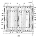
図1は、本発明の実施例1に係る半導体装置の要部の構成を示す平面図である。また、図2は、図1の半導体装置100のA−A線に沿った断面を示す断面図である。
FIG. 1 is a plan view showing a configuration of a main part of a semiconductor device according to
なお、ここでは、2つのMOS構造によりMOSキャパシタが構成される場合について説明する。また、MOSキャパシタがp型半導体基板上に設けられた場合について説明するが、導電型を逆にした場合でも適用される回路の極性を逆にすることにより同様に適用される。 Here, a case where a MOS capacitor is constituted by two MOS structures will be described. Although the case where the MOS capacitor is provided on the p-type semiconductor substrate will be described, the present invention is similarly applied by reversing the polarity of the applied circuit even when the conductivity type is reversed.
図1および図2に示すように、半導体装置100は、p型半導体基板1に形成されたMOS構造から構成されるMOSキャパシタ4と、このMOSキャパシタ4上に設けられた配線キャパシタ5とを備える。
As shown in FIGS. 1 and 2, the
上記MOS構造は、p型半導体基板1に形成されたn型ウェル6と、このn型ウェル6の表面に選択的に並んで形成されたドレイン領域、ソース領域となるp+拡散層7、8、9と、このp+拡散層7、8、9に挟まれた領域上に設けられたゲート絶縁膜10、11と、このゲート絶縁膜10、11上に設けられたゲート電極12、13と、バックゲートに電圧を印加するためのp+拡散層7、8、9を囲むようにn型ウェル6に形成されたn+拡散層14とを有する。
The MOS structure has an n-
MOSキャパシタ4は、上記MOS構造のドレイン領域となるp+拡散層7とソース領域となるp+拡散層8とが共通に接続されている。同様に、MOSキャパシタ4は、MOS構造のソース領域となるp+拡散層8とドレイン領域となるp+拡散層9とが共通に接続されている。
In the
配線キャパシタ5は、MOSキャパシタ4上に層間絶縁膜20を介して形成され、MOSキャパシタ4のゲート電極12、13とコンタクト15で接続されるとともに櫛歯状に延出した延出部16aを有する第1の櫛型配線16を有する。さらに、配線キャパシタ5は、MOSキャパシタ4上に層間絶縁膜20を介して形成されるとともに第1の櫛型配線16と線間絶縁膜21を介して配置され、p+拡散層7、8、9およびn+拡散層14に複数のコンタクト18、19で接続されるとともに櫛歯状に延出した延出部17aを有する第2の櫛型配線17、を有する。この第2の櫛型配線17と第1の櫛型配線16とは、対向して配置されている。
The
第2の櫛型配線17の延出部17aは、第1の櫛型配線16の延出部16aと交互に並んで配置されている。さらに、第2の櫛型配線17の延出部17aは、MOSキャパシタ4のドレイン領域となるp+拡散層7とソース領域となるp+拡散層8を結ぶチャネル方向に対して、同様にソース領域となるp+拡散層8とドレイン領域となるp+拡散層9を結ぶチャネル方向に対して、垂直に配置されている。
The extending
ここで、既述のように、第2の櫛型配線17の延出部17aは、線間絶縁膜21を介して第1の櫛型配線16の延出部16aと交互に並んで配置されている。そして、第1の櫛型配線16と第2の櫛型配線17とは、同じ配線層内に配置されている。これにより、第1の櫛型配線16の延出部16aと第2の櫛型配線17の延出部17aとが接近し、延出部16aと延出部17aとの間の線間絶縁膜21の容量を増加することができる。
Here, as described above, the extending
また、既述のように、第2の櫛型配線17の延出部17aは、MOSキャパシタ4のチャネル方向に対して垂直に配置されているので、第2の櫛型配線17の延出部17aは、p+拡散層7、8、9と複数のコンタクト18で接続することができる。これにより、コンタクト18によるコンタクト抵抗を低減することができる。
Further, as described above, the extending
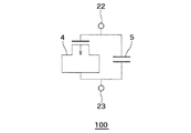
以上のような構成を有する半導体装置100の回路図は図3のように示される。図3に示すように、所望の電圧が印加される端子22と端子23の間に、MOSキャパシタ4と配線キャパシタ5とが接続される。
A circuit diagram of the
ここで、以上のような構成を有する半導体装置100の電圧依存性について説明する。
Here, the voltage dependence of the
まず、MOSキャパシタ4は、ゲート電圧Vg<0のときは、チャネルが形成されないが、アキュムレーション(accumulation)と呼ばれる蓄積状態であり空乏層が形成されないため容量Cは、ほぼゲート絶縁膜10、11の容量に等しい。したがって、半導体装置100の全体容量は、ほぼゲート絶縁膜10、11の容量と配線キャパシタ5の容量との和になる。
First, when the gate voltage Vg <0, the
次に、MOSキャパシタ4は、0<ゲート電圧Vg<しきい値電圧Vtのときは、ゲート電極直下のシリコン表面に空乏層が形成され、それにより生じる空乏層容量とゲート絶縁膜容量が直列接続された状態になる。したがって、MOSキャパシタ4の容量Cはゲート絶縁膜10、11の容量よりも小さくなる。しかし、配線キャパシタ5に形成される容量はゲート電圧に関係なく維持される。したがって、配線キャパシタ5を含めた半導体装置100の全体の容量として考えると、従来と比較して、電圧依存性を低減することができる。
Next, when 0 <gate voltage Vg <threshold voltage Vt,
次に、MOSキャパシタ4は、しきい値Vt以上のゲート電圧が印加されチャネルが形成されると、共通に接続されたp+拡散層7、8、9とMOS構造のゲート電極12、13との間にゲート絶縁膜10、11の静電容量を形成する。したがって、MOSキャパシタ4の容量Cは、ほぼゲート絶縁膜10、11の容量に等しい。これにより、半導体装置100の全体容量は、ほぼゲート絶縁膜10、11の容量と配線キャパシタ5の容量との和になる。
Next, when a gate voltage equal to or higher than the threshold value Vt is applied to form a channel, the
以上のように、半導体装置100は、従来と比較して、容量を増加しつつ、電圧依存性を低減することができる。
As described above, the
次に、以上のような構成を有する半導体装置100の周波数特性について説明する。
Next, frequency characteristics of the
まず、MOSキャパシタ4は、電源周波数が低周波である場合、MOSキャパシタ4のオンオフの切り替えで十分に反転層にキャリアが溜まるので反転層の容量が生じる。したがって、半導体装置100の全体容量は、ほぼゲート絶縁膜10、11の容量と配線キャパシタ5の容量との和になる。
First, when the power supply frequency of the
一方、MOSキャパシタ4は、電源周波数が低周波である場合、MOSキャパシタ4のオンオフの切り替えが速く反転層にキャリアが溜まらず反転層の容量が生じないことになる。しかし、配線キャパシタ5に形成される容量は電源周波数に関係なく維持される。したがって、配線キャパシタ5を含めた半導体装置100の全体の容量として考えると、従来と比較して、周波数特性を向上することができる。
On the other hand, when the power frequency of the
ここで、上記半導体装置100をチャージポンプ回路に適用した一例について説明する。
Here, an example in which the
図4は、本発明の実施例1に係る半導体装置を適用したチャージポンプ回路300を示す回路図である。
FIG. 4 is a circuit diagram showing a
図4に示すように、チャージポンプ回路300は、電源電圧が印加される入力端子30にソース領域が接続されるとともに、このソース領域にゲート電極が接続された入力MOSトランジスタ31と、この入力MOSトランジスタ31のドレイン領域と昇圧された電圧が出力される出力端子32との間で直列に接続されるとともにそのゲート電極がそのソース領域に接続された複数の昇圧MOSトランジスタ33と、この昇圧MOSトランジスタ33のソースに各々端子22(図2の第1の櫛型配線16)が接続された請求項1ないし4の何れかに記載の前記半導体装置と、を備える。
As shown in FIG. 4, the
隣接する半導体装置100の端子23(図2の第2の櫛型配線17)には、それぞれ互いに相補的なパルス信号Φ1、Φ2が入力される。
Pulse signals Φ1 and Φ2 that are complementary to each other are input to the terminals 23 (
上記チャージポンプ回路300は、入力端子に電源電圧が印加されるとともに相補的なクロック信号Φ1、Φ2が端子23にそれぞれ入力されると、昇圧動作し、出力端子32から昇圧された電圧を出力する。
When the power supply voltage is applied to the input terminal and complementary clock signals Φ1 and Φ2 are respectively input to the terminal 23, the
ここで、既述のように、半導体装置100は、従来のMOSキャパシタと比較して容量の電圧依存性が低減され周波数特性が向上されている。したがって、上記構成を有するチャージポンプ回路300は、従来と比較して、容量値の電圧依存性を低減しつつ容量値の周波数特性の向上し、昇圧能力を向上することができる。
Here, as described above, in the
以上のように、本実施例に係る半導体装置によれば、容量値の電圧依存性を低減しつつ、容量値の周波数特性を向上することができる。 As described above, according to the semiconductor device of this example, the frequency characteristic of the capacitance value can be improved while reducing the voltage dependency of the capacitance value.
実施例1では、配線キャパシタの櫛型配線の層が1層である場合について述べたが、本実施例では、配線キャパシタの櫛型配線の層が複数層である場合ついて述べる。 In the first embodiment, the case where the wiring capacitor has a single comb wiring layer is described. In this embodiment, the wiring capacitor has a plurality of comb wiring layers.
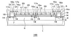
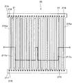
図5は、本発明の実施例2に係る半導体装置の配線キャパシタの要部構成を示す平面図である。また、図6は、図5の配線キャパシタの要部構成を示す斜視図である。また、図7は、図5のB−B線に沿った本発明の一態様である実施例2に係る半導体装置200の断面を示す断面図である。なお、図中、実施例1と同じ符号は、実施例1と同様の構成を示している。また、図5において、説明のため配線キャパシタの下層側については省略している。
FIG. 5 is a plan view showing the main configuration of the wiring capacitor of the semiconductor device according to the second embodiment of the present invention. FIG. 6 is a perspective view showing a configuration of a main part of the wiring capacitor of FIG. FIG. 7 is a cross-sectional view showing a cross section of the
図5ないし図7に示すように、半導体装置200は、p型半導体基板1に形成されたMOS構造で構成されるMOSキャパシタ4と、このMOSキャパシタ4上に設けられた配線キャパシタ25とを備える。
As shown in FIGS. 5 to 7, the
図6、図7に示すように、配線キャパシタ25は、MOSキャパシタ4上に層間絶縁膜20を介して形成され、MOSキャパシタ4のゲート電極12、13とコンタクト15で接続されるとともに櫛歯状に延出した延出部16aを有する第1の櫛型配線16を有する。
As shown in FIGS. 6 and 7, the
さらに、配線キャパシタ25は、MOSキャパシタ4上に層間絶縁膜20を介して形成されるとともに第1の櫛型配線16と線間絶縁膜21を介して配置され、p+拡散層7、8、9およびn+拡散層14に複数のコンタクト18、19で接続されるとともに櫛歯状に延出した延出部17aを有する第2の櫛型配線17を有する。
Further, the
また、配線キャパシタ25は、第1の櫛型配線16上に層間絶縁膜20を介して形成され、第1の櫛型配線16とコンタクト218で接続されるとともに櫛歯状に延出した延出部216aを有する第3の櫛型配線216を有する。
The
さらに、配線キャパシタ25は、第2の櫛型配線17上に層間絶縁膜20を介して形成されるとともに第3の櫛型配線216と線間絶縁膜21を介して配置され、第2の櫛型配線17とコンタクト219で接続されるとともに櫛歯状に延出した延出部217aを有する第4の櫛型配線217を有する。
Further, the
すなわち、配線キャパシタ25は、実施例1の配線キャパシタ5と比較して、第3の櫛型配線216と第4の櫛型配線217とが層間絶縁膜20を介して交互に積層された、多層配線層25aをさらに有する。
That is, the
ここで、図5ないし図7に示すように、第4の櫛型配線217の延出部217aは、第3の櫛型配線216の延出部216aと交互に並んで配置されている。そして、対となる第3の櫛型配線216と第4の櫛型配線217とは、同じ配線層内に配置されている。これにより、第3の櫛型配線216の延出部216aと第4の櫛型配線217の延出部217aとが接近し、延出部216aと延出部217aとの間の線間絶縁膜21の静電容量を増加することができる。
Here, as shown in FIGS. 5 to 7, the extending
既述のように、第4の櫛型配線217の延出部217aの下には層間絶縁膜20を介して第1の櫛型配線16の延出部16aが位置するとともに、第4の櫛型配線217の延出部217aの上には層間絶縁膜20を介して第3の櫛型配線216の延出部216aが位置している。
As described above, the
したがって、配線キャパシタ25の容量としては、これらの層間絶縁膜20の静電容量も含まれると考えられる。
Therefore, it is considered that the capacitance of the
以上のような構成を有する半導体装置200の回路図は、実施例1と同様に図3のように示される。
A circuit diagram of the
また、以上のような構成を有する半導体装置200の周波数特性、電圧依存性についても、配線キャパシタ25による容量が増加する点以外は、実施例1と同様である。
The frequency characteristics and voltage dependency of the
以上のように、本実施例に係る半導体装置によれば、容量値の電圧依存性を低減し容量値の周波数特性を向上しつつ、実施例1よりも大きな容量を得ることができる。 As described above, according to the semiconductor device of the present embodiment, it is possible to obtain a larger capacity than that of the first embodiment while reducing the voltage dependency of the capacitance value and improving the frequency characteristic of the capacitance value.
なお、本実施例についても、実施例1と同様にチャージポンプ回路に適用することにより、従来と比較して、容量値の電圧依存性を低減しつつ容量値の周波数特性の向上し、昇圧能力を向上することができる。 It should be noted that the present embodiment is also applied to the charge pump circuit in the same manner as the first embodiment, thereby improving the frequency characteristic of the capacitance value while reducing the voltage dependency of the capacitance value as compared with the prior art, and boosting capability. Can be improved.
また、本実施例においては、配線キャパシタの櫛型配線の多層配線層が2層である場合について説明したが、多層配線層を3層以上積層することにより、より有効にレイアウト面積を維持しつつ大きな静電容量を得ることができる。 Further, in this embodiment, the case where there are two multilayer wiring layers of the comb-shaped wiring of the wiring capacitor has been described, but the layout area can be maintained more effectively by stacking three or more multilayer wiring layers. A large capacitance can be obtained.
1 p型半導体基板
4 MOSキャパシタ
5 配線キャパシタ
6 n型ウェル
7、8、9 p+拡散層
10、11 ゲート絶縁膜
12、13 ゲート電極
14 n+拡散層
15 コンタクト
16 第1の櫛型配線
16a 延出部
17 第2の櫛型配線
17a 延出部
18、19 コンタクト
20 層間絶縁膜
21 線間絶縁膜
22、23 端子
25 配線キャパシタ
25a 多層配線層
30 入力端子
31 入力MOSトランジスタ
32 出力端子
33 昇圧MOSトランジスタ
100、200 半導体装置
216 第3の櫛型配線
216a 延出部
217 第4の櫛型配線
217a 延出部
218、219 コンタクト
300 チャージポンプ回路
1 p-
Claims (5)
前記MOSキャパシタ上に層間絶縁膜を介して形成され前記MOSキャパシタのゲート電極と接続されるとともに櫛歯状に延出した延出部を有する第1の櫛型配線、および、前記MOSキャパシタ上に層間絶縁膜を介して形成されるとともに前記第1の櫛型配線と線間絶縁膜を介して配置され前記ドレイン領域および前記ソース領域に接続されるとともに櫛歯状に延出した延出部を有する第2の櫛型配線、を有する配線キャパシタと、を備え、
前記第2の櫛型配線の延出部は、前記第1の櫛型配線の延出部と交互に並んで配置されているとともに、前記MOSキャパシタの前記ドレイン領域と前記ソース領域を結ぶチャネル方向に対して垂直に配置されていることを特徴とする半導体装置。 A drain region and a source region of a MOS structure are connected in common, the drain region connected in common, a MOS capacitor that forms a capacitance between the source region and the gate electrode of the MOS structure,
A first comb-shaped wiring formed on the MOS capacitor via an interlayer insulating film and connected to the gate electrode of the MOS capacitor and extending in a comb-tooth shape; and on the MOS capacitor An extension portion formed through an interlayer insulating film and disposed via the first comb-shaped wiring and the inter-line insulating film and connected to the drain region and the source region and extending in a comb shape A wiring capacitor having a second comb-shaped wiring having,
The extension portions of the second comb wiring are arranged alternately with the extension portions of the first comb wiring, and the channel direction connects the drain region and the source region of the MOS capacitor. A semiconductor device, wherein the semiconductor device is arranged perpendicular to the semiconductor device.
前記第4の櫛型配線の延出部は、前記第3の櫛型配線の延出部と交互に並んで配置されていることを特徴とする請求項2に記載の半導体装置。 The wiring capacitor is formed on the first comb-shaped wiring through an interlayer insulating film, and is connected to the first comb-shaped wiring by a contact and has a third extending portion extending in a comb shape. And the second comb-shaped wiring formed on the second comb-shaped wiring via an interlayer insulating film and disposed via the third comb-shaped wiring and the inter-line insulating film. And a fourth wiring having a comb-like extension extending in contact with each other and a multilayer wiring layer laminated via an interlayer insulating film,
3. The semiconductor device according to claim 2, wherein the extended portions of the fourth comb wiring are arranged alternately with the extended portions of the third comb wiring. 4.
電源電圧が印加される入力端子にソース領域が接続された入力MOSトランジスタと、
前記入力MOSトランジスタのドレイン領域と昇圧された電圧が出力される出力端子との間で直列に接続された複数の昇圧MOSトランジスタと、を備え、
前記昇圧MOSトランジスタのソース領域に各々前記第1の櫛型配線が接続され、
隣接する前記半導体装置の前記第2の櫛型配線には、それぞれ互いに相補的なパルス信号が入力されることを特徴とするチャージポンプ回路。 A drain region and a source region of a MOS structure are connected in common, the drain region connected in common, a MOS capacitor that forms a capacitance between the source region and the gate electrode of the MOS structure, and the MOS A first comb-shaped wiring formed on the capacitor through an interlayer insulating film and connected to the gate electrode of the MOS capacitor and extending in a comb-like shape; and an interlayer insulation on the MOS capacitor A first portion formed through a film and disposed through the first comb-shaped wiring and the inter-line insulating film and connected to the drain region and the source region and having an extending portion extending in a comb-like shape; A wiring capacitor having two comb-shaped wirings, and the extending portions of the second comb-shaped wiring are arranged alternately with the extending portions of the first comb-shaped wiring. A semiconductor device which is arranged perpendicular to the channel direction connecting said source region and said drain region of said MOS capacitor,
An input MOS transistor having a source region connected to an input terminal to which a power supply voltage is applied;
A plurality of boosting MOS transistors connected in series between the drain region of the input MOS transistor and an output terminal from which the boosted voltage is output;
The first comb wiring is connected to the source region of the boost MOS transistor,
A charge pump circuit, wherein pulse signals complementary to each other are input to the second comb wirings of the adjacent semiconductor devices.
Priority Applications (2)
| Application Number | Priority Date | Filing Date | Title |
|---|---|---|---|
| JP2006026782A JP4908006B2 (en) | 2006-02-03 | 2006-02-03 | Semiconductor device |
| US11/670,605 US7557400B2 (en) | 2006-02-03 | 2007-02-02 | Semiconductor device in which capacitance of a MOS capacitor is complemented with the capacitance of a wiring capacitor |
Applications Claiming Priority (1)
| Application Number | Priority Date | Filing Date | Title |
|---|---|---|---|
| JP2006026782A JP4908006B2 (en) | 2006-02-03 | 2006-02-03 | Semiconductor device |
Publications (2)
| Publication Number | Publication Date |
|---|---|
| JP2007208101A JP2007208101A (en) | 2007-08-16 |
| JP4908006B2 true JP4908006B2 (en) | 2012-04-04 |
Family
ID=38333164
Family Applications (1)
| Application Number | Title | Priority Date | Filing Date |
|---|---|---|---|
| JP2006026782A Expired - Fee Related JP4908006B2 (en) | 2006-02-03 | 2006-02-03 | Semiconductor device |
Country Status (2)
| Country | Link |
|---|---|
| US (1) | US7557400B2 (en) |
| JP (1) | JP4908006B2 (en) |
Families Citing this family (18)
| Publication number | Priority date | Publication date | Assignee | Title |
|---|---|---|---|---|
| JP2008226998A (en) * | 2007-03-09 | 2008-09-25 | Matsushita Electric Ind Co Ltd | Semiconductor integrated circuit |
| JP5072731B2 (en) | 2008-06-23 | 2012-11-14 | 株式会社東芝 | Constant voltage boost power supply |
| US20110168782A1 (en) * | 2010-01-12 | 2011-07-14 | Nxp B.V. | Capacitance under a fringe capacitor of a radio frquency integrated circuit |
| FR2965942B1 (en) * | 2010-10-08 | 2013-02-22 | Commissariat Energie Atomique | LIQUID CRYSTAL DISPLAY OF TRANSMISSIVE TYPE IN CMOS TECHNOLOGY WITH AUXILIARY STORAGE CAPACITY |
| US8916919B2 (en) | 2011-06-23 | 2014-12-23 | International Business Machines Corporation | Interdigitated vertical native capacitor |
| TWI463674B (en) * | 2011-09-06 | 2014-12-01 | 群聯電子股份有限公司 | Capacitive structure suitable for use in integrated circuits |
| CN103000624B (en) * | 2011-09-19 | 2015-07-01 | 群联电子股份有限公司 | Capacitive structure suitable for application in integrated circuits |
| JP5947580B2 (en) * | 2012-03-23 | 2016-07-06 | ローム株式会社 | Decoupled capacitor cell, cell-based IC, cell-based IC layout system and layout method |
| JP6161267B2 (en) * | 2012-11-28 | 2017-07-12 | ルネサスエレクトロニクス株式会社 | Capacitor and charge pump circuit |
| US20150137201A1 (en) * | 2013-11-20 | 2015-05-21 | Qualcomm Incorporated | High density linear capacitor |
| US9640532B2 (en) * | 2014-02-14 | 2017-05-02 | Qualcomm Incorporated | Stacked metal oxide semiconductor (MOS) and metal oxide metal (MOM) capacitor architecture |
| US9703313B2 (en) * | 2014-10-20 | 2017-07-11 | Ambiq Micro, Inc. | Peripheral clock management |
| US9583479B1 (en) * | 2016-01-14 | 2017-02-28 | Globalfoundries Inc. | Semiconductor charge pump with imbedded capacitor |
| JP7103780B2 (en) * | 2017-11-27 | 2022-07-20 | ラピスセミコンダクタ株式会社 | Semiconductor equipment |
| US10763263B2 (en) * | 2019-01-30 | 2020-09-01 | Micron Technology, Inc. | Semiconductor device having equivalent series resistance unit |
| CN115315807A (en) | 2020-03-30 | 2022-11-08 | 索尼半导体解决方案公司 | Semiconductor device and electronic apparatus |
| CN115528024A (en) * | 2021-06-25 | 2022-12-27 | 瑞昱半导体股份有限公司 | Compact capacitor structure |
| CN115275010A (en) * | 2022-07-25 | 2022-11-01 | 圣邦微电子(北京)股份有限公司 | MOM capacitor and charge pump circuit |
Family Cites Families (12)
| Publication number | Priority date | Publication date | Assignee | Title |
|---|---|---|---|---|
| JPS61263251A (en) * | 1985-05-17 | 1986-11-21 | Nec Corp | Semiconductor device |
| JPH03293759A (en) * | 1990-04-12 | 1991-12-25 | Fuji Electric Co Ltd | Capacitor to be incorporated into mos integrated circuit device |
| JPH0473960A (en) * | 1990-07-16 | 1992-03-09 | Nec Ic Microcomput Syst Ltd | Integrated circuit |
| KR0183739B1 (en) * | 1995-09-19 | 1999-03-20 | 김광호 | Semiconductor device comprising decoupling capacitor and method of manufacturing same |
| TW393655B (en) * | 1997-03-24 | 2000-06-11 | Seiko Epson Corp | Semiconductor capacitance device and semiconductor device for made by using the same |
| JP2000057790A (en) * | 1998-08-05 | 2000-02-25 | Ricoh Co Ltd | Voltage generation circuit |
| CN1291352A (en) * | 1998-12-16 | 2001-04-11 | 因芬尼昂技术股份公司 | Integrated circuit with capacity element |
| US6037622A (en) * | 1999-03-29 | 2000-03-14 | Winbond Electronics Corporation | Charge pump circuits for low supply voltages |
| JP2002217304A (en) * | 2000-11-17 | 2002-08-02 | Rohm Co Ltd | Semiconductor device |
| JP2004241762A (en) * | 2003-01-16 | 2004-08-26 | Nec Electronics Corp | Semiconductor device |
| JP4751035B2 (en) * | 2004-06-09 | 2011-08-17 | 株式会社東芝 | Semiconductor integrated circuit and booster circuit |
| US7768044B2 (en) * | 2004-07-30 | 2010-08-03 | Agere Systems Inc. | Metal capacitor stacked with a MOS capacitor to provide increased capacitance density |
-
2006
- 2006-02-03 JP JP2006026782A patent/JP4908006B2/en not_active Expired - Fee Related
-
2007
- 2007-02-02 US US11/670,605 patent/US7557400B2/en active Active
Also Published As
| Publication number | Publication date |
|---|---|
| US7557400B2 (en) | 2009-07-07 |
| US20070181918A1 (en) | 2007-08-09 |
| JP2007208101A (en) | 2007-08-16 |
Similar Documents
| Publication | Publication Date | Title |
|---|---|---|
| US7557400B2 (en) | Semiconductor device in which capacitance of a MOS capacitor is complemented with the capacitance of a wiring capacitor | |
| US7436015B2 (en) | Driver for driving a load using a charge pump circuit | |
| US5598029A (en) | Power supply wiring for semiconductor device | |
| US7834377B2 (en) | Semiconductor integrated circuit device | |
| US9496403B2 (en) | Semiconductor device and method of manufacturing the same | |
| US4635088A (en) | High speed-low power consuming IGFET integrated circuit | |
| CN104183628A (en) | Semiconductor device | |
| JP6983905B2 (en) | Semiconductor device | |
| JP5058644B2 (en) | Neuron MOS transistor | |
| JP2013143446A (en) | Capacitive element, semiconductor device and electronic apparatus | |
| JPH02228063A (en) | High frequency integrated circuit channel capacitor | |
| JPS61180475A (en) | Charge transfer device | |
| JP2001358335A (en) | Semiconductor device | |
| US9559178B2 (en) | Non-volatile memory (NVM) cell and device structure integration | |
| KR100257641B1 (en) | Semiconductor integrated circuit with differential circuit | |
| JP4110792B2 (en) | Capacitor element and semiconductor integrated circuit using capacitor element | |
| KR101162771B1 (en) | High voltage operating field effect transistor, and bias circuit therefor and high voltage circuit thereof | |
| JPWO2013018589A1 (en) | Semiconductor integrated circuit device | |
| JP2005072233A (en) | Semiconductor device | |
| JP2003060042A (en) | Semiconductor device | |
| JP2000150789A (en) | Semiconductor integrated circuit | |
| TW518697B (en) | Production-method of field-effect-transistors in integrated semiconductor-circuits and an integrated semiconductor-circuit produced with such a field-effect-transistor | |
| TW200414433A (en) | LSI alleviating hysteresis of delay time | |
| JP2001068552A (en) | Semiconductor integrated circuit device | |
| JP2000101022A (en) | Semiconductor integrated circuit device |
Legal Events
| Date | Code | Title | Description |
|---|---|---|---|
| A621 | Written request for application examination |
Free format text: JAPANESE INTERMEDIATE CODE: A621 Effective date: 20080805 |
|
| A977 | Report on retrieval |
Free format text: JAPANESE INTERMEDIATE CODE: A971007 Effective date: 20111212 |
|
| TRDD | Decision of grant or rejection written | ||
| A01 | Written decision to grant a patent or to grant a registration (utility model) |
Free format text: JAPANESE INTERMEDIATE CODE: A01 Effective date: 20111216 |
|
| A01 | Written decision to grant a patent or to grant a registration (utility model) |
Free format text: JAPANESE INTERMEDIATE CODE: A01 |
|
| A61 | First payment of annual fees (during grant procedure) |
Free format text: JAPANESE INTERMEDIATE CODE: A61 Effective date: 20120112 |
|
| FPAY | Renewal fee payment (event date is renewal date of database) |
Free format text: PAYMENT UNTIL: 20150120 Year of fee payment: 3 |
|
| FPAY | Renewal fee payment (event date is renewal date of database) |
Free format text: PAYMENT UNTIL: 20150120 Year of fee payment: 3 |
|
| LAPS | Cancellation because of no payment of annual fees |