JP4905595B2 - Organic thin film solar cell, organic thin film solar cell module, and organic thin film solar cell manufacturing method - Google Patents
Organic thin film solar cell, organic thin film solar cell module, and organic thin film solar cell manufacturing method Download PDFInfo
- Publication number
- JP4905595B2 JP4905595B2 JP2011010852A JP2011010852A JP4905595B2 JP 4905595 B2 JP4905595 B2 JP 4905595B2 JP 2011010852 A JP2011010852 A JP 2011010852A JP 2011010852 A JP2011010852 A JP 2011010852A JP 4905595 B2 JP4905595 B2 JP 4905595B2
- Authority
- JP
- Japan
- Prior art keywords
- layer
- film
- solar cell
- electrode layer
- transparent electrode
- Prior art date
- Legal status (The legal status is an assumption and is not a legal conclusion. Google has not performed a legal analysis and makes no representation as to the accuracy of the status listed.)
- Expired - Fee Related
Links
- 239000010409 thin film Substances 0.000 title claims description 98
- 238000004519 manufacturing process Methods 0.000 title claims description 32
- 239000010408 film Substances 0.000 claims description 289
- 239000000758 substrate Substances 0.000 claims description 128
- 238000006243 chemical reaction Methods 0.000 claims description 81
- 239000013078 crystal Substances 0.000 claims description 69
- 229910044991 metal oxide Inorganic materials 0.000 claims description 51
- 150000004706 metal oxides Chemical class 0.000 claims description 51
- 238000000576 coating method Methods 0.000 claims description 49
- 238000005224 laser annealing Methods 0.000 claims description 38
- 239000011248 coating agent Substances 0.000 claims description 34
- 229920001609 Poly(3,4-ethylenedioxythiophene) Polymers 0.000 claims description 22
- 229920000172 poly(styrenesulfonic acid) Polymers 0.000 claims description 9
- 229940005642 polystyrene sulfonic acid Drugs 0.000 claims description 9
- 239000010410 layer Substances 0.000 description 466
- 238000000034 method Methods 0.000 description 79
- 239000000463 material Substances 0.000 description 48
- 239000002253 acid Substances 0.000 description 31
- 229910052751 metal Inorganic materials 0.000 description 21
- 239000002184 metal Substances 0.000 description 21
- 229920001940 conductive polymer Polymers 0.000 description 20
- 239000002861 polymer material Substances 0.000 description 20
- 238000000605 extraction Methods 0.000 description 16
- 230000008569 process Effects 0.000 description 15
- 150000001875 compounds Chemical class 0.000 description 12
- 230000007423 decrease Effects 0.000 description 11
- -1 polyphenylene vinylene Polymers 0.000 description 11
- 230000009467 reduction Effects 0.000 description 11
- 230000002378 acidificating effect Effects 0.000 description 10
- 229920001577 copolymer Polymers 0.000 description 9
- 238000005530 etching Methods 0.000 description 9
- 230000015572 biosynthetic process Effects 0.000 description 8
- 239000007788 liquid Substances 0.000 description 8
- 238000004544 sputter deposition Methods 0.000 description 8
- 239000012044 organic layer Substances 0.000 description 7
- 229920000553 poly(phenylenevinylene) Polymers 0.000 description 7
- 229920000642 polymer Polymers 0.000 description 7
- PXHVJJICTQNCMI-UHFFFAOYSA-N Nickel Chemical compound [Ni] PXHVJJICTQNCMI-UHFFFAOYSA-N 0.000 description 6
- 238000002425 crystallisation Methods 0.000 description 6
- 230000008025 crystallization Effects 0.000 description 6
- 238000009413 insulation Methods 0.000 description 6
- 238000004528 spin coating Methods 0.000 description 6
- 229910052782 aluminium Inorganic materials 0.000 description 5
- 238000000137 annealing Methods 0.000 description 5
- 230000004888 barrier function Effects 0.000 description 5
- 238000001035 drying Methods 0.000 description 5
- 230000001747 exhibiting effect Effects 0.000 description 5
- 229920000767 polyaniline Polymers 0.000 description 5
- 239000002356 single layer Substances 0.000 description 5
- 239000002904 solvent Substances 0.000 description 5
- 229920002799 BoPET Polymers 0.000 description 4
- 229910004298 SiO 2 Inorganic materials 0.000 description 4
- 239000011575 calcium Substances 0.000 description 4
- 230000001678 irradiating effect Effects 0.000 description 4
- DCZNSJVFOQPSRV-UHFFFAOYSA-N n,n-diphenyl-4-[4-(n-phenylanilino)phenyl]aniline Chemical compound C1=CC=CC=C1N(C=1C=CC(=CC=1)C=1C=CC(=CC=1)N(C=1C=CC=CC=1)C=1C=CC=CC=1)C1=CC=CC=C1 DCZNSJVFOQPSRV-UHFFFAOYSA-N 0.000 description 4
- 150000002894 organic compounds Chemical class 0.000 description 4
- 229920000123 polythiophene Polymers 0.000 description 4
- 239000000523 sample Substances 0.000 description 4
- 229910052709 silver Inorganic materials 0.000 description 4
- 239000010936 titanium Substances 0.000 description 4
- 238000001771 vacuum deposition Methods 0.000 description 4
- UHOVQNZJYSORNB-UHFFFAOYSA-N Benzene Chemical compound C1=CC=CC=C1 UHOVQNZJYSORNB-UHFFFAOYSA-N 0.000 description 3
- UJOBWOGCFQCDNV-UHFFFAOYSA-N Carbazole Natural products C1=CC=C2C3=CC=CC=C3NC2=C1 UJOBWOGCFQCDNV-UHFFFAOYSA-N 0.000 description 3
- 229910018487 Ni—Cr Inorganic materials 0.000 description 3
- 229920000265 Polyparaphenylene Polymers 0.000 description 3
- HSFWRNGVRCDJHI-UHFFFAOYSA-N alpha-acetylene Natural products C#C HSFWRNGVRCDJHI-UHFFFAOYSA-N 0.000 description 3
- 238000007611 bar coating method Methods 0.000 description 3
- 229910052791 calcium Inorganic materials 0.000 description 3
- VNNRSPGTAMTISX-UHFFFAOYSA-N chromium nickel Chemical compound [Cr].[Ni] VNNRSPGTAMTISX-UHFFFAOYSA-N 0.000 description 3
- 239000010949 copper Substances 0.000 description 3
- 238000007607 die coating method Methods 0.000 description 3
- 230000000694 effects Effects 0.000 description 3
- 239000010931 gold Substances 0.000 description 3
- 230000001771 impaired effect Effects 0.000 description 3
- 239000002346 layers by function Substances 0.000 description 3
- 238000007645 offset printing Methods 0.000 description 3
- BASFCYQUMIYNBI-UHFFFAOYSA-N platinum Chemical compound [Pt] BASFCYQUMIYNBI-UHFFFAOYSA-N 0.000 description 3
- 229920001197 polyacetylene Polymers 0.000 description 3
- 229920000128 polypyrrole Polymers 0.000 description 3
- 239000011347 resin Substances 0.000 description 3
- 229920005989 resin Polymers 0.000 description 3
- 238000007650 screen-printing Methods 0.000 description 3
- 238000002834 transmittance Methods 0.000 description 3
- CJVYYDCBKKKIPD-UHFFFAOYSA-N 1-n,1-n,2-n,2-n-tetramethylbenzene-1,2-diamine Chemical compound CN(C)C1=CC=CC=C1N(C)C CJVYYDCBKKKIPD-UHFFFAOYSA-N 0.000 description 2
- STTGYIUESPWXOW-UHFFFAOYSA-N 2,9-dimethyl-4,7-diphenyl-1,10-phenanthroline Chemical compound C=12C=CC3=C(C=4C=CC=CC=4)C=C(C)N=C3C2=NC(C)=CC=1C1=CC=CC=C1 STTGYIUESPWXOW-UHFFFAOYSA-N 0.000 description 2
- 239000002841 Lewis acid Substances 0.000 description 2
- 239000002879 Lewis base Substances 0.000 description 2
- 229910052581 Si3N4 Inorganic materials 0.000 description 2
- VYPSYNLAJGMNEJ-UHFFFAOYSA-N Silicium dioxide Chemical compound O=[Si]=O VYPSYNLAJGMNEJ-UHFFFAOYSA-N 0.000 description 2
- XUIMIQQOPSSXEZ-UHFFFAOYSA-N Silicon Chemical compound [Si] XUIMIQQOPSSXEZ-UHFFFAOYSA-N 0.000 description 2
- RTAQQCXQSZGOHL-UHFFFAOYSA-N Titanium Chemical compound [Ti] RTAQQCXQSZGOHL-UHFFFAOYSA-N 0.000 description 2
- 238000002441 X-ray diffraction Methods 0.000 description 2
- 229910052783 alkali metal Inorganic materials 0.000 description 2
- 150000001340 alkali metals Chemical class 0.000 description 2
- 229910052784 alkaline earth metal Inorganic materials 0.000 description 2
- 150000001342 alkaline earth metals Chemical class 0.000 description 2
- XAGFODPZIPBFFR-UHFFFAOYSA-N aluminium Chemical compound [Al] XAGFODPZIPBFFR-UHFFFAOYSA-N 0.000 description 2
- MWPLVEDNUUSJAV-UHFFFAOYSA-N anthracene Chemical compound C1=CC=CC2=CC3=CC=CC=C3C=C21 MWPLVEDNUUSJAV-UHFFFAOYSA-N 0.000 description 2
- 239000011324 bead Substances 0.000 description 2
- 239000000919 ceramic Substances 0.000 description 2
- 239000011651 chromium Substances 0.000 description 2
- 230000000052 comparative effect Effects 0.000 description 2
- 230000021615 conjugation Effects 0.000 description 2
- 239000000470 constituent Substances 0.000 description 2
- 229910052802 copper Inorganic materials 0.000 description 2
- LNDJVIYUJOJFSO-UHFFFAOYSA-N cyanoacetylene Chemical group C#CC#N LNDJVIYUJOJFSO-UHFFFAOYSA-N 0.000 description 2
- 238000010586 diagram Methods 0.000 description 2
- 238000009792 diffusion process Methods 0.000 description 2
- 238000003618 dip coating Methods 0.000 description 2
- 238000011156 evaluation Methods 0.000 description 2
- 229910052737 gold Inorganic materials 0.000 description 2
- 238000007756 gravure coating Methods 0.000 description 2
- 229910052738 indium Inorganic materials 0.000 description 2
- AMGQUBHHOARCQH-UHFFFAOYSA-N indium;oxotin Chemical compound [In].[Sn]=O AMGQUBHHOARCQH-UHFFFAOYSA-N 0.000 description 2
- 238000007733 ion plating Methods 0.000 description 2
- 150000007517 lewis acids Chemical class 0.000 description 2
- 150000007527 lewis bases Chemical class 0.000 description 2
- 229910052744 lithium Inorganic materials 0.000 description 2
- 238000000691 measurement method Methods 0.000 description 2
- 150000002739 metals Chemical class 0.000 description 2
- 238000002156 mixing Methods 0.000 description 2
- 229910052759 nickel Inorganic materials 0.000 description 2
- 239000011368 organic material Substances 0.000 description 2
- 238000000059 patterning Methods 0.000 description 2
- 230000035699 permeability Effects 0.000 description 2
- 125000000843 phenylene group Chemical group C1(=C(C=CC=C1)*)* 0.000 description 2
- 229920000301 poly(3-hexylthiophene-2,5-diyl) polymer Polymers 0.000 description 2
- 229920002098 polyfluorene Polymers 0.000 description 2
- 238000010248 power generation Methods 0.000 description 2
- 238000007639 printing Methods 0.000 description 2
- 230000001681 protective effect Effects 0.000 description 2
- BBEAQIROQSPTKN-UHFFFAOYSA-N pyrene Chemical compound C1=CC=C2C=CC3=CC=CC4=CC=C1C2=C43 BBEAQIROQSPTKN-UHFFFAOYSA-N 0.000 description 2
- 238000000926 separation method Methods 0.000 description 2
- 229910052710 silicon Inorganic materials 0.000 description 2
- 239000010703 silicon Substances 0.000 description 2
- HQVNEWCFYHHQES-UHFFFAOYSA-N silicon nitride Chemical compound N12[Si]34N5[Si]62N3[Si]51N64 HQVNEWCFYHHQES-UHFFFAOYSA-N 0.000 description 2
- 229910052814 silicon oxide Inorganic materials 0.000 description 2
- 238000005507 spraying Methods 0.000 description 2
- 239000000126 substance Substances 0.000 description 2
- 238000010998 test method Methods 0.000 description 2
- NLDYACGHTUPAQU-UHFFFAOYSA-N tetracyanoethylene Chemical group N#CC(C#N)=C(C#N)C#N NLDYACGHTUPAQU-UHFFFAOYSA-N 0.000 description 2
- PCCVSPMFGIFTHU-UHFFFAOYSA-N tetracyanoquinodimethane Chemical compound N#CC(C#N)=C1C=CC(=C(C#N)C#N)C=C1 PCCVSPMFGIFTHU-UHFFFAOYSA-N 0.000 description 2
- 229910052719 titanium Inorganic materials 0.000 description 2
- 238000012546 transfer Methods 0.000 description 2
- 229920002554 vinyl polymer Polymers 0.000 description 2
- XLYOFNOQVPJJNP-UHFFFAOYSA-N water Chemical compound O XLYOFNOQVPJJNP-UHFFFAOYSA-N 0.000 description 2
- 229910000838 Al alloy Inorganic materials 0.000 description 1
- 229910017008 AsF 6 Inorganic materials 0.000 description 1
- XMWRBQBLMFGWIX-UHFFFAOYSA-N C60 fullerene Chemical class C12=C3C(C4=C56)=C7C8=C5C5=C9C%10=C6C6=C4C1=C1C4=C6C6=C%10C%10=C9C9=C%11C5=C8C5=C8C7=C3C3=C7C2=C1C1=C2C4=C6C4=C%10C6=C9C9=C%11C5=C5C8=C3C3=C7C1=C1C2=C4C6=C2C9=C5C3=C12 XMWRBQBLMFGWIX-UHFFFAOYSA-N 0.000 description 1
- OYPRJOBELJOOCE-UHFFFAOYSA-N Calcium Chemical compound [Ca] OYPRJOBELJOOCE-UHFFFAOYSA-N 0.000 description 1
- OKTJSMMVPCPJKN-UHFFFAOYSA-N Carbon Chemical compound [C] OKTJSMMVPCPJKN-UHFFFAOYSA-N 0.000 description 1
- VYZAMTAEIAYCRO-UHFFFAOYSA-N Chromium Chemical compound [Cr] VYZAMTAEIAYCRO-UHFFFAOYSA-N 0.000 description 1
- RYGMFSIKBFXOCR-UHFFFAOYSA-N Copper Chemical compound [Cu] RYGMFSIKBFXOCR-UHFFFAOYSA-N 0.000 description 1
- 229910000881 Cu alloy Inorganic materials 0.000 description 1
- XEEYBQQBJWHFJM-UHFFFAOYSA-N Iron Chemical compound [Fe] XEEYBQQBJWHFJM-UHFFFAOYSA-N 0.000 description 1
- 229910001030 Iron–nickel alloy Inorganic materials 0.000 description 1
- 229910052772 Samarium Inorganic materials 0.000 description 1
- BQCADISMDOOEFD-UHFFFAOYSA-N Silver Chemical compound [Ag] BQCADISMDOOEFD-UHFFFAOYSA-N 0.000 description 1
- 229910052771 Terbium Inorganic materials 0.000 description 1
- 229910001069 Ti alloy Inorganic materials 0.000 description 1
- ATJFFYVFTNAWJD-UHFFFAOYSA-N Tin Chemical compound [Sn] ATJFFYVFTNAWJD-UHFFFAOYSA-N 0.000 description 1
- 229910052769 Ytterbium Inorganic materials 0.000 description 1
- 238000010521 absorption reaction Methods 0.000 description 1
- 230000001154 acute effect Effects 0.000 description 1
- 239000000654 additive Substances 0.000 description 1
- 239000012790 adhesive layer Substances 0.000 description 1
- 238000007605 air drying Methods 0.000 description 1
- 230000003373 anti-fouling effect Effects 0.000 description 1
- 229910052788 barium Inorganic materials 0.000 description 1
- 238000005452 bending Methods 0.000 description 1
- CREMABGTGYGIQB-UHFFFAOYSA-N carbon carbon Chemical compound C.C CREMABGTGYGIQB-UHFFFAOYSA-N 0.000 description 1
- 239000011203 carbon fibre reinforced carbon Substances 0.000 description 1
- 239000002041 carbon nanotube Substances 0.000 description 1
- 229910021393 carbon nanotube Inorganic materials 0.000 description 1
- 238000005266 casting Methods 0.000 description 1
- 229910052804 chromium Inorganic materials 0.000 description 1
- 229910017052 cobalt Inorganic materials 0.000 description 1
- 239000010941 cobalt Substances 0.000 description 1
- GUTLYIVDDKVIGB-UHFFFAOYSA-N cobalt atom Chemical compound [Co] GUTLYIVDDKVIGB-UHFFFAOYSA-N 0.000 description 1
- 239000004020 conductor Substances 0.000 description 1
- 229920000547 conjugated polymer Polymers 0.000 description 1
- 229920001795 coordination polymer Polymers 0.000 description 1
- 230000006866 deterioration Effects 0.000 description 1
- 238000011161 development Methods 0.000 description 1
- 239000006185 dispersion Substances 0.000 description 1
- 238000004090 dissolution Methods 0.000 description 1
- 238000005516 engineering process Methods 0.000 description 1
- 150000002148 esters Chemical class 0.000 description 1
- 125000005678 ethenylene group Chemical group [H]C([*:1])=C([H])[*:2] 0.000 description 1
- 238000001704 evaporation Methods 0.000 description 1
- 239000000945 filler Substances 0.000 description 1
- GVEPBJHOBDJJJI-UHFFFAOYSA-N fluoranthrene Natural products C1=CC(C2=CC=CC=C22)=C3C2=CC=CC3=C1 GVEPBJHOBDJJJI-UHFFFAOYSA-N 0.000 description 1
- 238000007429 general method Methods 0.000 description 1
- PCHJSUWPFVWCPO-UHFFFAOYSA-N gold Chemical compound [Au] PCHJSUWPFVWCPO-UHFFFAOYSA-N 0.000 description 1
- 238000007646 gravure printing Methods 0.000 description 1
- 150000002366 halogen compounds Chemical class 0.000 description 1
- 238000010438 heat treatment Methods 0.000 description 1
- 125000005842 heteroatom Chemical group 0.000 description 1
- APFVFJFRJDLVQX-UHFFFAOYSA-N indium atom Chemical compound [In] APFVFJFRJDLVQX-UHFFFAOYSA-N 0.000 description 1
- PQXKHYXIUOZZFA-UHFFFAOYSA-M lithium fluoride Inorganic materials [Li+].[F-] PQXKHYXIUOZZFA-UHFFFAOYSA-M 0.000 description 1
- 229920002521 macromolecule Polymers 0.000 description 1
- 229910052749 magnesium Inorganic materials 0.000 description 1
- 230000007246 mechanism Effects 0.000 description 1
- 239000012528 membrane Substances 0.000 description 1
- 239000000203 mixture Substances 0.000 description 1
- 229910000623 nickel–chromium alloy Inorganic materials 0.000 description 1
- 230000003287 optical effect Effects 0.000 description 1
- 238000001259 photo etching Methods 0.000 description 1
- IEQIEDJGQAUEQZ-UHFFFAOYSA-N phthalocyanine Chemical compound N1C(N=C2C3=CC=CC=C3C(N=C3C4=CC=CC=C4C(=N4)N3)=N2)=C(C=CC=C2)C2=C1N=C1C2=CC=CC=C2C4=N1 IEQIEDJGQAUEQZ-UHFFFAOYSA-N 0.000 description 1
- 238000005268 plasma chemical vapour deposition Methods 0.000 description 1
- 229920003023 plastic Polymers 0.000 description 1
- 239000004033 plastic Substances 0.000 description 1
- 238000007747 plating Methods 0.000 description 1
- 229910052697 platinum Inorganic materials 0.000 description 1
- 229920003227 poly(N-vinyl carbazole) Polymers 0.000 description 1
- 229920000548 poly(silane) polymer Polymers 0.000 description 1
- 229920001088 polycarbazole Polymers 0.000 description 1
- 150000004032 porphyrins Chemical class 0.000 description 1
- 229910052700 potassium Inorganic materials 0.000 description 1
- 230000027756 respiratory electron transport chain Effects 0.000 description 1
- 239000003566 sealing material Substances 0.000 description 1
- 239000004065 semiconductor Substances 0.000 description 1
- 239000004332 silver Substances 0.000 description 1
- 239000010944 silver (metal) Substances 0.000 description 1
- 239000007787 solid Substances 0.000 description 1
- 239000010935 stainless steel Substances 0.000 description 1
- 229910001220 stainless steel Inorganic materials 0.000 description 1
- 229910052712 strontium Inorganic materials 0.000 description 1
- 229910052715 tantalum Inorganic materials 0.000 description 1
- GUVRBAGPIYLISA-UHFFFAOYSA-N tantalum atom Chemical compound [Ta] GUVRBAGPIYLISA-UHFFFAOYSA-N 0.000 description 1
- 238000012360 testing method Methods 0.000 description 1
- 238000002230 thermal chemical vapour deposition Methods 0.000 description 1
- 238000001291 vacuum drying Methods 0.000 description 1
- 238000007740 vapor deposition Methods 0.000 description 1
- 239000013585 weight reducing agent Substances 0.000 description 1
- 229910052726 zirconium Inorganic materials 0.000 description 1
Images


Classifications
-
- B—PERFORMING OPERATIONS; TRANSPORTING
- B82—NANOTECHNOLOGY
- B82Y—SPECIFIC USES OR APPLICATIONS OF NANOSTRUCTURES; MEASUREMENT OR ANALYSIS OF NANOSTRUCTURES; MANUFACTURE OR TREATMENT OF NANOSTRUCTURES
- B82Y10/00—Nanotechnology for information processing, storage or transmission, e.g. quantum computing or single electron logic
-
- H—ELECTRICITY
- H01—ELECTRIC ELEMENTS
- H01G—CAPACITORS; CAPACITORS, RECTIFIERS, DETECTORS, SWITCHING DEVICES OR LIGHT-SENSITIVE DEVICES, OF THE ELECTROLYTIC TYPE
- H01G9/00—Electrolytic capacitors, rectifiers, detectors, switching devices, light-sensitive or temperature-sensitive devices; Processes of their manufacture
- H01G9/20—Light-sensitive devices
- H01G9/2095—Light-sensitive devices comprising a flexible sustrate
-
- H—ELECTRICITY
- H01—ELECTRIC ELEMENTS
- H01L—SEMICONDUCTOR DEVICES NOT COVERED BY CLASS H10
- H01L31/00—Semiconductor devices sensitive to infrared radiation, light, electromagnetic radiation of shorter wavelength or corpuscular radiation and specially adapted either for the conversion of the energy of such radiation into electrical energy or for the control of electrical energy by such radiation; Processes or apparatus specially adapted for the manufacture or treatment thereof or of parts thereof; Details thereof
- H01L31/02—Details
- H01L31/0224—Electrodes
- H01L31/022466—Electrodes made of transparent conductive layers, e.g. TCO, ITO layers
-
- H—ELECTRICITY
- H01—ELECTRIC ELEMENTS
- H01L—SEMICONDUCTOR DEVICES NOT COVERED BY CLASS H10
- H01L31/00—Semiconductor devices sensitive to infrared radiation, light, electromagnetic radiation of shorter wavelength or corpuscular radiation and specially adapted either for the conversion of the energy of such radiation into electrical energy or for the control of electrical energy by such radiation; Processes or apparatus specially adapted for the manufacture or treatment thereof or of parts thereof; Details thereof
- H01L31/18—Processes or apparatus specially adapted for the manufacture or treatment of these devices or of parts thereof
- H01L31/1884—Manufacture of transparent electrodes, e.g. TCO, ITO
-
- H—ELECTRICITY
- H01—ELECTRIC ELEMENTS
- H01M—PROCESSES OR MEANS, e.g. BATTERIES, FOR THE DIRECT CONVERSION OF CHEMICAL ENERGY INTO ELECTRICAL ENERGY
- H01M14/00—Electrochemical current or voltage generators not provided for in groups H01M6/00 - H01M12/00; Manufacture thereof
-
- H—ELECTRICITY
- H10—SEMICONDUCTOR DEVICES; ELECTRIC SOLID-STATE DEVICES NOT OTHERWISE PROVIDED FOR
- H10K—ORGANIC ELECTRIC SOLID-STATE DEVICES
- H10K77/00—Constructional details of devices covered by this subclass and not covered by groups H10K10/80, H10K30/80, H10K50/80 or H10K59/80
- H10K77/10—Substrates, e.g. flexible substrates
- H10K77/111—Flexible substrates
-
- H—ELECTRICITY
- H10—SEMICONDUCTOR DEVICES; ELECTRIC SOLID-STATE DEVICES NOT OTHERWISE PROVIDED FOR
- H10K—ORGANIC ELECTRIC SOLID-STATE DEVICES
- H10K30/00—Organic devices sensitive to infrared radiation, light, electromagnetic radiation of shorter wavelength or corpuscular radiation
- H10K30/30—Organic devices sensitive to infrared radiation, light, electromagnetic radiation of shorter wavelength or corpuscular radiation comprising bulk heterojunctions, e.g. interpenetrating networks of donor and acceptor material domains
-
- H—ELECTRICITY
- H10—SEMICONDUCTOR DEVICES; ELECTRIC SOLID-STATE DEVICES NOT OTHERWISE PROVIDED FOR
- H10K—ORGANIC ELECTRIC SOLID-STATE DEVICES
- H10K85/00—Organic materials used in the body or electrodes of devices covered by this subclass
- H10K85/10—Organic polymers or oligomers
- H10K85/111—Organic polymers or oligomers comprising aromatic, heteroaromatic, or aryl chains, e.g. polyaniline, polyphenylene or polyphenylene vinylene
- H10K85/113—Heteroaromatic compounds comprising sulfur or selene, e.g. polythiophene
- H10K85/1135—Polyethylene dioxythiophene [PEDOT]; Derivatives thereof
-
- H—ELECTRICITY
- H10—SEMICONDUCTOR DEVICES; ELECTRIC SOLID-STATE DEVICES NOT OTHERWISE PROVIDED FOR
- H10K—ORGANIC ELECTRIC SOLID-STATE DEVICES
- H10K85/00—Organic materials used in the body or electrodes of devices covered by this subclass
- H10K85/20—Carbon compounds, e.g. carbon nanotubes or fullerenes
- H10K85/211—Fullerenes, e.g. C60
- H10K85/215—Fullerenes, e.g. C60 comprising substituents, e.g. PCBM
-
- Y—GENERAL TAGGING OF NEW TECHNOLOGICAL DEVELOPMENTS; GENERAL TAGGING OF CROSS-SECTIONAL TECHNOLOGIES SPANNING OVER SEVERAL SECTIONS OF THE IPC; TECHNICAL SUBJECTS COVERED BY FORMER USPC CROSS-REFERENCE ART COLLECTIONS [XRACs] AND DIGESTS
- Y02—TECHNOLOGIES OR APPLICATIONS FOR MITIGATION OR ADAPTATION AGAINST CLIMATE CHANGE
- Y02E—REDUCTION OF GREENHOUSE GAS [GHG] EMISSIONS, RELATED TO ENERGY GENERATION, TRANSMISSION OR DISTRIBUTION
- Y02E10/00—Energy generation through renewable energy sources
- Y02E10/50—Photovoltaic [PV] energy
- Y02E10/542—Dye sensitized solar cells
Description
本発明は、導電性金属酸化物を含有する透明電極層を有する有機薄膜太陽電池に関するものである。 The present invention relates to an organic thin film solar cell having a transparent electrode layer containing a conductive metal oxide.
太陽電池において、受光側の電極は透明電極とされる。従来、この透明電極には、酸化インジウム錫(ITO)等の導電性金属酸化物が用いられており、中でも、導電性や透明性が高く、仕事関数が高いことから、ITOが主に使用されている。
しかしながら、太陽電池に用いられるITO電極は、厚みが薄く、シート抵抗が大きいため、発生した電流がITO電極を通過する際に消費され、発電効率が低下するという問題がある。この現象は、太陽電池の面積が大きくなるにつれて顕著に現れる。
In the solar cell, the electrode on the light receiving side is a transparent electrode. Conventionally, conductive metal oxides such as indium tin oxide (ITO) have been used for this transparent electrode. Among them, ITO is mainly used because of its high conductivity and transparency and high work function. ing.
However, since the ITO electrode used for the solar cell is thin and has a large sheet resistance, there is a problem that the generated current is consumed when passing through the ITO electrode and power generation efficiency is lowered. This phenomenon becomes more prominent as the area of the solar cell increases.
ITO電極の低抵抗化の手法としては、アニール処理が提案されている(例えば特許文献1参照)。また、ITO膜にレーザーを照射することにより結晶化し、電気伝導性を向上させる研究も行われている(例えば非特許文献1参照)。さらに、ITO以外にも、n型またはp型半導体の性質を示す金属酸化物、例えばインジウムや錫等の酸化物の層にレーザーを照射することにより結晶化することが提案されている(例えば特許文献2参照)。これらの方法はレーザーアニール法を利用するものである。 An annealing process has been proposed as a technique for reducing the resistance of the ITO electrode (see, for example, Patent Document 1). In addition, studies have been made to crystallize an ITO film by irradiating a laser to improve electrical conductivity (for example, see Non-Patent Document 1). Further, in addition to ITO, it has been proposed to crystallize a metal oxide exhibiting n-type or p-type semiconductor properties, for example, an oxide layer such as indium or tin by irradiating a laser (for example, a patent). Reference 2). These methods use a laser annealing method.
しかしながら、ITO電極をアニール処理により結晶化すると、ITO電極が脆くなるという問題がある。特に、フレキシブル太陽電池では、曲げた際にITO電極が割れてしまい、変換効率が低下するという問題が生じる。また、フレキシブル太陽電池では可撓性を有するフィルム基板が用いられるが、フィルム基板は耐熱性が低いため、フィルム基板上にITO電極を形成する場合にはアニール処理を行うことは困難である。 However, when the ITO electrode is crystallized by annealing, there is a problem that the ITO electrode becomes brittle. In particular, in a flexible solar cell, the ITO electrode breaks when bent, resulting in a problem that the conversion efficiency is lowered. In addition, although a flexible film substrate is used in the flexible solar cell, since the film substrate has low heat resistance, it is difficult to perform an annealing process when forming an ITO electrode on the film substrate.
また、特に有機薄膜太陽電池においては、光電変換層から電極への電荷の取出しが容易に行われるように、電極と光電変換層との間にバッファー層が設けられる場合がある。このバッファー層には、ポリエチレンジオキシチオフェン/ポリスチレンスルホン酸(PEDOT/PSS)が採用されることが多い。しかしながら、PEDOT/PSSを含む塗工液は酸性を示すため、電極上にPEDOT/PSSを含む塗工液を塗布してバッファー層を形成すると、酸によって電極が溶解する等のダメージを受けるおそれがある。また、バッファー層が吸湿した場合には、バッファー層中でPEDOT/PSSが酸性を示すものとなるので、同様に電極がダメージを受けるおそれがある。 In particular, in an organic thin film solar cell, a buffer layer may be provided between the electrode and the photoelectric conversion layer so that the charge can be easily taken out from the photoelectric conversion layer to the electrode. In this buffer layer, polyethylenedioxythiophene / polystyrene sulfonic acid (PEDOT / PSS) is often employed. However, since the coating liquid containing PEDOT / PSS shows acidity, when a coating liquid containing PEDOT / PSS is applied on the electrode to form a buffer layer, there is a risk of damage such as dissolution of the electrode by the acid. is there. Further, when the buffer layer absorbs moisture, PEDOT / PSS in the buffer layer shows acidity, and the electrode may be similarly damaged.
本発明は、上記問題点に鑑みてなされたものであり、低抵抗および可撓性を併せ持つ電極を有し、さらには酸による電極へのダメージを低減することが可能な有機薄膜太陽電池を提供することを主目的とする。 The present invention has been made in view of the above problems, and provides an organic thin-film solar cell having an electrode having both low resistance and flexibility , and further capable of reducing damage to the electrode due to acid. The main purpose is to do.
本発明者は上記課題を解決するために鋭意検討を重ねた結果、導電性金属酸化物を含有する非晶質膜の表面のみをレーザーアニールにより結晶化することにより、低抵抗、可撓性、耐酸性を兼ね備える透明電極層が得られることを見出し、本発明を完成させるに至った。 As a result of intensive studies in order to solve the above problems, the present inventor crystallized only the surface of an amorphous film containing a conductive metal oxide by laser annealing, so that low resistance, flexibility, The inventors have found that a transparent electrode layer having acid resistance can be obtained, and have completed the present invention.
本発明は、可撓性を有する透明基板と、上記透明基板上に形成された透明電極層と、上記透明電極上に形成されたポリエチレンジオキシチオフェン/ポリスチレンスルホン酸を含有するバッファー層と、上記バッファー層上に形成された光電変換層と、上記光電変換層上に形成された対向電極層とを有する有機薄膜太陽電池であって、上記透明電極層は、上記透明基板上に形成され、導電性金属酸化物を含有する非晶質膜と、上記非晶質膜上に形成され、上記非晶質膜に含有される上記導電性金属酸化物と同一の導電性金属酸化物を含有する結晶膜とを有することを特徴とする有機薄膜太陽電池を提供する。 The present invention provides a transparent substrate having flexibility, a transparent electrode layer formed on the transparent substrate, a buffer layer containing polyethylenedioxythiophene / polystyrenesulfonic acid formed on the transparent electrode, An organic thin film solar cell having a photoelectric conversion layer formed on a buffer layer and a counter electrode layer formed on the photoelectric conversion layer , wherein the transparent electrode layer is formed on the transparent substrate and is conductive An amorphous film containing a conductive metal oxide, and a crystal formed on the amorphous film and containing the same conductive metal oxide as the conductive metal oxide contained in the amorphous film An organic thin film solar cell comprising a film is provided.
本発明によれば、透明電極層が同一の導電性金属酸化物を含有する非晶質膜および結晶膜を有するので、低抵抗および可撓性を併せ持つ透明電極層とすることが可能である。また、結晶膜は非晶質膜が結晶化されたものであるので非晶質膜よりも耐酸性に優れており、この結晶膜はバッファー層側に形成されているので、バッファー層が酸性を示す材料を含有する場合には、非晶質膜が結晶膜によって保護され、バッファー層に含有される酸の影響による透明電極層のダメージを低減することができ、有機薄膜太陽電池の信頼性を向上させることが可能となる。 According to the present invention, since the transparent electrode layer has an amorphous film and a crystal film containing the same conductive metal oxide, a transparent electrode layer having both low resistance and flexibility can be obtained. In addition, since the crystalline film is a crystallized amorphous film, it has better acid resistance than the amorphous film. Since this crystalline film is formed on the buffer layer side, the buffer layer is made acidic. In the case of containing the material shown, the amorphous film is protected by the crystal film, and the damage of the transparent electrode layer due to the influence of the acid contained in the buffer layer can be reduced, thereby improving the reliability of the organic thin film solar cell. It becomes possible to improve.
上記発明においては、上記透明基板と上記透明電極層との間に断熱層が形成されていてもよい。断熱層によって透明電極層を形成する際のアニール処理時の熱から透明基板を保護することができるからである。特に、可撓性を有する透明基板は耐熱性に劣る傾向にあることから断熱層が形成されていることが好ましい。In the said invention, the heat insulation layer may be formed between the said transparent substrate and the said transparent electrode layer. This is because the transparent substrate can be protected from heat during the annealing process when the transparent electrode layer is formed by the heat insulating layer. In particular, since a transparent substrate having flexibility tends to be inferior in heat resistance, a heat insulating layer is preferably formed.
さらに本発明は、上述の有機薄膜太陽電池が複数個直列または並列に接続されていることを特徴とする有機薄膜太陽電池モジュールを提供する。 Furthermore, the present invention provides an organic thin film solar cell module, wherein a plurality of the above organic thin film solar cells are connected in series or in parallel.
また本発明は、可撓性を有する透明基板と、上記透明基板上に形成された透明電極層と、上記透明電極上に形成されたポリエチレンジオキシチオフェン/ポリスチレンスルホン酸を含有するバッファー層と、上記バッファー層上に形成された光電変換層と、上記光電変換層上に形成された対向電極層とを有する有機薄膜太陽電池の製造方法であって、上記透明基板上に導電性金属酸化物を含有する非晶質膜を形成した後、上記非晶質膜の表面をレーザーアニールにより結晶化して結晶膜を形成し、上記非晶質膜および上記結晶膜を有する透明電極層を得る透明電極層形成工程と、上記透明電極層上に、ポリエチレンジオキシチオフェン/ポリスチレンスルホン酸を含有するバッファー層形成用塗工液を塗布してバッファー層を形成するバッファー層形成工程とを有することを特徴とする有機薄膜太陽電池の製造方法を提供する。 The present invention also includes a transparent substrate having flexibility, a transparent electrode layer formed on the transparent substrate, a buffer layer containing polyethylenedioxythiophene / polystyrenesulfonic acid formed on the transparent electrode, A method for producing an organic thin film solar cell, comprising: a photoelectric conversion layer formed on the buffer layer; and a counter electrode layer formed on the photoelectric conversion layer, wherein a conductive metal oxide is formed on the transparent substrate. After forming the amorphous film to be contained, the surface of the amorphous film is crystallized by laser annealing to form a crystalline film, thereby obtaining the transparent film layer having the amorphous film and the crystalline film Forming a buffer layer by applying a coating solution for forming a buffer layer containing polyethylenedioxythiophene / polystyrenesulfonic acid on the transparent electrode layer; It provides a method for manufacturing an organic thin film solar cell and having an over layer forming step.
本発明によれば、非晶質膜の表面をレーザーアニールにより結晶化して結晶膜を形成し、非晶質膜および結晶膜を有する透明電極層を得るので、低抵抗および可撓性を併せ持つ透明電極層を形成することが可能である。結晶膜は非晶質膜が結晶化されたものであるので非晶質膜よりも耐酸性に優れているため、透明電極層上に酸性を示すバッファー層形成用塗工液を塗布してバッファー層を形成する場合には、酸の影響による透明電極層のダメージを低減することが可能である。したがって、信頼性の高い有機薄膜太陽電池を得ることができる。 According to the present invention, the surface of the amorphous film is crystallized by laser annealing to form a crystalline film, and the transparent electrode layer having the amorphous film and the crystalline film is obtained. Therefore, the transparent film having both low resistance and flexibility is obtained. An electrode layer can be formed. Since the crystalline film is a crystallized amorphous film, it has better acid resistance than the amorphous film. Therefore, a buffer layer forming coating solution that shows acidity is applied onto the transparent electrode layer to buffer the crystalline film. When forming a layer, it is possible to reduce damage to the transparent electrode layer due to the influence of an acid. Therefore, a highly reliable organic thin film solar cell can be obtained.
本発明においては、透明電極層が同一の導電性金属酸化物を含有する非晶質膜および結晶膜を有するので、低抵抗および可撓性を兼ね備え、さらには耐酸性をも併せ持つ透明電極層を有する有機薄膜太陽電池とすることが可能であるという効果を奏する。 In the present invention, since the transparent electrode layer has an amorphous film and a crystal film containing the same conductive metal oxide, a transparent electrode layer having both low resistance and flexibility and also having acid resistance is provided. There exists an effect that it can be set as the organic thin film solar cell which has .
以下、本発明の太陽電池用基板、有機薄膜太陽電池、有機薄膜太陽電池モジュール、太陽電池用基板の製造方法、および有機薄膜太陽電池の製造方法について詳細に説明する。 Hereinafter, the solar cell substrate, organic thin film solar cell, organic thin film solar cell module, solar cell substrate manufacturing method, and organic thin film solar cell manufacturing method of the present invention will be described in detail.
A.太陽電池用基板
まず、本発明の太陽電池用基板について説明する。
本発明の太陽電池用基板は、透明基板と、上記透明基板上に形成された透明電極層とを有する太陽電池用基板であって、上記透明電極層は、上記透明基板上に形成され、導電性金属酸化物を含有する非晶質膜と、上記非晶質膜上に形成され、上記非晶質膜に含有される上記導電性金属酸化物と同一の導電性金属酸化物を含有する結晶膜とを有することを特徴とするものである。
A. First, the solar cell substrate of the present invention will be described.
The solar cell substrate of the present invention is a solar cell substrate having a transparent substrate and a transparent electrode layer formed on the transparent substrate, wherein the transparent electrode layer is formed on the transparent substrate and is electrically conductive. An amorphous film containing a conductive metal oxide, and a crystal formed on the amorphous film and containing the same conductive metal oxide as the conductive metal oxide contained in the amorphous film And a film.
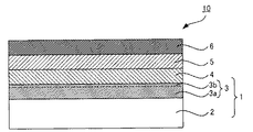
本発明の太陽電池用基板について図面を参照しながら説明する。
図1は、本発明の太陽電池用基板の一例を示す概略断面図である。図1に示す例において、太陽電池用基板1は、透明基板2と、透明基板2上に形成され、導電性金属酸化物を含有する透明電極層3とを有している。透明電極層3は、透明基板2上に形成され、導電性金属酸化物を含有する非晶質膜3aと、非晶質膜3a上に形成され、導電性金属酸化物を含有する結晶膜3bとを有する。非晶質膜3aおよび結晶膜3bは同一の導電性金属酸化物を含有し、結晶膜3bは非晶質膜3aの表面を結晶化することで得られる。
The solar cell substrate of the present invention will be described with reference to the drawings.
FIG. 1 is a schematic cross-sectional view showing an example of the solar cell substrate of the present invention. In the example shown in FIG. 1, a
一般的に、導電性金属酸化物において、結晶膜は非晶質膜よりも抵抗が低く、すなわち導電性が高い。また、導電性金属酸化物において、結晶膜は非晶質膜よりも耐酸性に優れている。さらに、導電性金属酸化物において、非晶質膜と結晶膜とでは仕事関数が異なるものとなる。 In general, in a conductive metal oxide, a crystalline film has a lower resistance than an amorphous film, that is, has high conductivity. In the conductive metal oxide, the crystal film has better acid resistance than the amorphous film. Further, in the conductive metal oxide, the work function is different between the amorphous film and the crystal film.
本発明によれば、透明電極層が非晶質膜よりも抵抗が低い結晶膜を有することにより、透明電極層自体の導電性を高めることが可能である。また、透明電極層が可撓性に優れる非晶質膜を有することにより、透明電極層自体の可撓性を維持することが可能である。したがって本発明においては、低抵抗および可撓性を併せ持つ透明電極層とすることができる。 According to the present invention, since the transparent electrode layer has a crystal film having a resistance lower than that of the amorphous film, the conductivity of the transparent electrode layer itself can be increased. Further, since the transparent electrode layer has an amorphous film having excellent flexibility, it is possible to maintain the flexibility of the transparent electrode layer itself. Therefore, in the present invention, a transparent electrode layer having both low resistance and flexibility can be obtained.
また本発明によれば、透明基板が可撓性を有するフィルム基板である場合には、透明電極層が非晶質膜を有し可撓性に優れているので、本発明の太陽電池用基板を用いることにより高性能なフレキシブル太陽電池を得ることが可能である。 According to the invention, when the transparent substrate is a flexible film substrate, the transparent electrode layer has an amorphous film and is excellent in flexibility. It is possible to obtain a high-performance flexible solar cell by using
図2は、本発明の太陽電池用基板を有する有機薄膜太陽電池の一例を示す概略断面図である。図2に示す有機薄膜太陽電池10は、太陽電池用基板1と、透明電極層3上に形成されたバッファー層4と、バッファー層4上に形成された光電変換層5と、光電変換層5上に形成された対向電極層6とを有している。
FIG. 2 is a schematic cross-sectional view showing an example of an organic thin-film solar cell having the solar cell substrate of the present invention. An organic thin film
本発明によれば、透明電極層が非晶質膜および結晶膜を有し、耐酸性に優れる結晶膜がバッファー層側に形成されている。そのため、図2に示すような有機薄膜太陽電池において、バッファー層が酸性を示す材料を含有する場合には、バッファー層が非晶質膜に直に接触することがなく、結晶膜によって非晶質膜が保護されるので、バッファー層に含まれる酸の影響による透明電極層のダメージを低減することが可能である。これにより、酸の影響によって透明電極層が溶解して、透明電極層の電気的特性が低下するのを抑制することができる。その結果、有機薄膜太陽電池の信頼性の向上を図ることが可能となる。
したがって本発明においては、透明電極層を低抵抗化しつつ、酸による透明電極層のダメージを抑制し、電気的性能を向上させることが可能である。
According to the present invention, the transparent electrode layer has an amorphous film and a crystal film, and the crystal film having excellent acid resistance is formed on the buffer layer side. Therefore, in the organic thin film solar cell as shown in FIG. 2, when the buffer layer contains an acidic material, the buffer layer is not in direct contact with the amorphous film, and the Since the film is protected, damage to the transparent electrode layer due to the influence of the acid contained in the buffer layer can be reduced. Thereby, it can suppress that a transparent electrode layer melt | dissolves by the influence of an acid and the electrical property of a transparent electrode layer falls. As a result, it becomes possible to improve the reliability of the organic thin film solar cell.
Therefore, in the present invention, the resistance of the transparent electrode layer can be reduced, the damage of the transparent electrode layer due to acid can be suppressed, and the electrical performance can be improved.
図3は、本発明の太陽電池用基板を有する有機薄膜太陽電池の他の例を示す概略断面図である。図3に示す有機薄膜太陽電池20は、太陽電池用基板1と、透明電極層3上に形成された有機層15と、有機層15上に形成された対向電極層6とを有している。
FIG. 3 is a schematic cross-sectional view showing another example of an organic thin-film solar cell having the solar cell substrate of the present invention. The organic thin film
本発明によれば、透明電極層の非晶質膜と結晶膜とでは仕事関数が異なるので、図3に示すような有機薄膜太陽電池において、透明電極層と有機層との界面で仕事関数を調整することが可能である。例えば、結晶膜の仕事関数と透明電極層に直に接する有機層の仕事関数との差が、非晶質膜の仕事関数と透明電極層に直に接する有機層の仕事関数との差よりも小さい場合には、有機層から透明電極層への電荷移動性を向上させることが可能となる。 According to the present invention, since the work function is different between the amorphous film and the crystal film of the transparent electrode layer, in the organic thin film solar cell as shown in FIG. 3, the work function is set at the interface between the transparent electrode layer and the organic layer. It is possible to adjust. For example, the difference between the work function of the crystalline film and the work function of the organic layer in direct contact with the transparent electrode layer is greater than the difference between the work function of the amorphous film and the work function of the organic layer in direct contact with the transparent electrode layer. When it is small, the charge mobility from the organic layer to the transparent electrode layer can be improved.
以下、本発明の太陽電池用基板における各構成について説明する。 Hereafter, each structure in the board | substrate for solar cells of this invention is demonstrated.
1.透明電極層
本発明における透明電極層は、透明基板上に形成されるものであり、透明基板上に形成され、導電性金属酸化物を含有する非晶質膜と、非晶質膜上に形成され、非晶質膜に含有される導電性金属酸化物と同一の導電性金属酸化物を含有する結晶膜とを有するものである。非晶質膜および結晶膜は同一の導電性金属酸化物を含有し、結晶膜は非晶質膜の表面を結晶化することにより得られる。なお、非晶質膜を結晶化させて結晶膜を得る過程で導電性金属酸化物の元素組成が変化したとしても、その非晶質膜に含有される導電性金属酸化物と結晶膜に含有される導電性金属酸化物は同一のものとする。
1. Transparent electrode layer The transparent electrode layer in the present invention is formed on a transparent substrate, formed on the transparent substrate, and formed on the amorphous film containing the conductive metal oxide and the amorphous film. And a crystalline film containing the same conductive metal oxide as the conductive metal oxide contained in the amorphous film. The amorphous film and the crystalline film contain the same conductive metal oxide, and the crystalline film is obtained by crystallizing the surface of the amorphous film. Even if the elemental composition of the conductive metal oxide changes during the process of crystallizing the amorphous film to obtain the crystal film, the conductive metal oxide contained in the amorphous film and the crystal film contain it. The conductive metal oxides to be used are the same.
なお、透明電極層が非晶質膜および結晶膜を有することは、透明電極層をエッチングすることで確認することができる。具体的には、透明電極層と、層全体が非晶質膜である電極層と、層全体が結晶膜である電極層とについて、エッチングレートを比較することで、透明電極層が非晶質膜および結晶膜を有することを確認することができる。まず、層全体が非晶質膜である電極層と、層全体が結晶膜である電極層とについて、あらかじめ、酸性エッチング液により任意の時間で腐食した後、膜厚の減少量を段差計で測定しておく。結晶膜は非晶質膜よりも耐酸性に優れているため、結晶膜の膜厚の減少量は非晶質膜の膜厚の減少量よりも少なくなる。次いで、透明電極層を酸性エッチング液により任意の時間で腐食した後、膜厚の減少量を段差計で測定する。透明電極層の膜厚の減少量が、層全体が非晶質膜である電極層の膜厚の減少量と、層全体が結晶膜である電極層の膜厚の減少量との間の範囲内である場合には、透明電極層は非晶質膜および結晶膜を有すると判定する。 In addition, it can confirm that a transparent electrode layer has an amorphous film | membrane and a crystalline film by etching a transparent electrode layer. Specifically, the transparent electrode layer is amorphous by comparing the etching rates of the transparent electrode layer, the electrode layer whose whole layer is an amorphous film, and the electrode layer whose whole layer is a crystalline film. It can be confirmed that the film has a film and a crystal film. First, for an electrode layer whose whole layer is an amorphous film and an electrode layer whose whole layer is a crystalline film, after corroding with an acidic etching solution for an arbitrary time in advance, the amount of decrease in film thickness is measured with a step gauge. Keep measuring. Since the crystal film has better acid resistance than the amorphous film, the amount of decrease in the film thickness of the crystal film is smaller than the amount of decrease in the film thickness of the amorphous film. Next, after the transparent electrode layer is corroded with an acidic etching solution for an arbitrary time, the amount of film thickness reduction is measured with a step gauge. The amount of decrease in the thickness of the transparent electrode layer ranges between the amount of decrease in the thickness of the electrode layer whose entire layer is an amorphous film and the amount of decrease in the thickness of the electrode layer whose entire layer is a crystalline film. If it is within the range, the transparent electrode layer is determined to have an amorphous film and a crystalline film.
透明電極層は、通常、光電変換層で発生した正孔を取り出すための電極(正孔取出し電極)とされる。本発明において、透明電極層は透明性を有し、透明電極層側が受光面となる。 The transparent electrode layer is usually an electrode (hole extraction electrode) for extracting holes generated in the photoelectric conversion layer. In the present invention, the transparent electrode layer has transparency, and the transparent electrode layer side is the light receiving surface.
非晶質膜および結晶膜に用いられる導電性金属酸化物としては、導電性および透明性を有し、アモルファス構造および結晶構造を持ち、結晶化により抵抗が低く耐酸性が高くなり得るものであり、アニール処理により結晶化され得るものであれば特に限定されるものではない。このような導電性金属酸化物としては、酸化インジウム錫(ITO)が好ましく用いられる。ITOは、導電性および透明性を有し、かつ仕事関数が高いからである。また、ITOを用いた場合にはレーザーアニールにより層表面のみを結晶化することができるからである。 Conductive metal oxides used for amorphous films and crystal films are conductive and transparent, have an amorphous structure and a crystal structure, and can have low resistance and high acid resistance due to crystallization. There is no particular limitation as long as it can be crystallized by annealing treatment. As such a conductive metal oxide, indium tin oxide (ITO) is preferably used. This is because ITO has conductivity and transparency and has a high work function. Further, when ITO is used, only the layer surface can be crystallized by laser annealing.
結晶膜は、導電性金属酸化物が結晶構造を有するときの仕事関数と同程度の仕事関数を有することが好ましい。すなわち、透明電極層の表面は、導電性金属酸化物が結晶構造を有するときの仕事関数と同程度の仕事関数を有するようになるまで結晶化されていることが好ましい。結晶膜の仕事関数は導電性金属酸化物の種類に応じて異なる。例えば導電性金属酸化物がITOである場合、結晶膜は4.6eV〜4.9eV程度の仕事関数を有することが好ましい。
なお、結晶膜の仕事関数は、透明電極層の結晶膜が形成されている側の表面の仕事関数を測定することにより求めることができる。
The crystal film preferably has a work function comparable to that when the conductive metal oxide has a crystal structure. That is, it is preferable that the surface of the transparent electrode layer is crystallized until it has a work function comparable to that when the conductive metal oxide has a crystal structure. The work function of the crystal film varies depending on the type of conductive metal oxide. For example, when the conductive metal oxide is ITO, the crystal film preferably has a work function of about 4.6 eV to 4.9 eV.
The work function of the crystal film can be obtained by measuring the work function of the surface of the transparent electrode layer on which the crystal film is formed.
透明電極層のシート抵抗は、100Ω/□以下であることが好ましく、中でも50Ω/□以下、特に20Ω/□以下であることが好ましい。非晶質膜および結晶膜を有する透明電極層のシート抵抗が上記範囲であれば、十分な導電性が得られる。
なお、上記シート抵抗は、三菱化学株式会社製 表面抵抗計(ロレスタMCP:四端子プローブ)を用い、JIS R1637(ファインセラミックス薄膜の抵抗率試験方法:4探針法による測定方法)に基づき、測定した値である。
The sheet resistance of the transparent electrode layer is preferably 100Ω / □ or less, more preferably 50Ω / □ or less, and particularly preferably 20Ω / □ or less. If the sheet resistance of the transparent electrode layer having an amorphous film and a crystal film is in the above range, sufficient conductivity can be obtained.
In addition, the said sheet resistance is measured based on JIS R1637 (Resistance test method of fine ceramics thin film: Measurement method by 4 probe method) using a surface resistance meter (Loresta MCP: Four-terminal probe) manufactured by Mitsubishi Chemical Corporation. It is the value.
透明電極層の膜厚としては、0.1nm〜500nmの範囲内であることが好ましく、中でも10nm〜300nmの範囲内であることが好ましい。膜厚が上記範囲より薄いと、透明電極層のシート抵抗が大きくなりすぎ、発生した電荷を十分に外部回路へ伝達できない可能性があり、一方、膜厚が上記範囲より厚いと、全光線透過率が低下し、光電変換効率を低下させる可能性があるからである。 The film thickness of the transparent electrode layer is preferably in the range of 0.1 nm to 500 nm, and more preferably in the range of 10 nm to 300 nm. If the film thickness is smaller than the above range, the sheet resistance of the transparent electrode layer may become too large, and the generated charge may not be sufficiently transmitted to the external circuit. This is because the rate may decrease and the photoelectric conversion efficiency may decrease.
透明電極層中の結晶膜の厚みとしては、透明電極層が可撓性を有するような厚みであればよい。結晶膜の厚みが厚いと透明電極層の可撓性が損なわれるおそれがある。したがって、透明電極層の可撓性を高めるために、結晶膜の厚みは比較的薄いことが好ましい。
また、本発明の太陽電池用基板が有機薄膜太陽電池用基板である場合、透明電極層中の結晶膜の厚みとしては、耐酸性を有する厚みであればよい。結晶膜の厚みが薄いと所望の耐酸性が得られない場合がある。一方、結晶膜の厚みが厚いと透明電極層の可撓性が損なわれる。結晶膜の厚みが一定以上であれば十分な耐酸性を得ることができる。したがって、透明電極層の可撓性を高めるために、結晶膜の厚みは耐酸性を有する厚みの中でも比較的薄いことが好ましい。
The thickness of the crystal film in the transparent electrode layer may be such that the transparent electrode layer has flexibility. If the crystal film is thick, the flexibility of the transparent electrode layer may be impaired. Therefore, in order to increase the flexibility of the transparent electrode layer, the thickness of the crystal film is preferably relatively thin.
Further, when the solar cell substrate of the present invention is an organic thin film solar cell substrate, the thickness of the crystal film in the transparent electrode layer may be any thickness that has acid resistance. If the crystal film is thin, desired acid resistance may not be obtained. On the other hand, if the crystal film is thick, the flexibility of the transparent electrode layer is impaired. If the thickness of the crystal film is equal to or greater than a certain level, sufficient acid resistance can be obtained. Therefore, in order to increase the flexibility of the transparent electrode layer, the thickness of the crystal film is preferably relatively thin among the acid-resistant thicknesses.
透明電極層の全光線透過率は85%以上であることが好ましく、中でも90%以上、特に92%以上であることが好ましい。透明電極層の全光線透過率が上記範囲であることにより、透明電極層にて光を十分に透過することができ、光電変換層にて光を効率的に吸収することができるからである。
なお、上記全光線透過率は、可視光領域において、スガ試験機株式会社製 SMカラーコンピュータ(型番:SM−C)を用いて測定した値である。
The total light transmittance of the transparent electrode layer is preferably 85% or more, more preferably 90% or more, and particularly preferably 92% or more. This is because when the total light transmittance of the transparent electrode layer is within the above range, light can be sufficiently transmitted through the transparent electrode layer, and light can be efficiently absorbed by the photoelectric conversion layer.
The total light transmittance is a value measured using an SM color computer (model number: SM-C) manufactured by Suga Test Instruments Co., Ltd. in the visible light region.
透明電極層は、透明基板上に全面に形成されていてもよく、パターン状に形成されていてもよい。
また、結晶膜3bは、図1に例示するように非晶質膜3a上に全面に形成されていてもよく、図4に例示するように非晶質膜3a上にパターン状に形成されていてもよい。結晶膜が非晶質膜上にパターン状に形成されている場合、例えば図5に示すような有機薄膜太陽電池10が得られる。このような場合でも、素子性能を高めることが可能である。
The transparent electrode layer may be formed on the entire surface of the transparent substrate, or may be formed in a pattern.
Further, the
なお、透明電極層の形成方法については、後述の「D.太陽電池用基板の製造方法」の項に記載するので、ここでの説明は省略する。 The method for forming the transparent electrode layer will be described later in the section “ D. Method for manufacturing a solar cell substrate”, and will not be described here.
2.透明基板
本発明に用いられる透明基板は、上記透明電極層を支持するものである。
2. Transparent substrate The transparent substrate used in the present invention supports the transparent electrode layer.
透明基板としては特に限定されるものではなく、例えば透明樹脂フィルム、光学用樹脂板等の可撓性を有する透明なフレキシブル材を挙げることができる。
透明樹脂フィルムは、加工性に優れており、製造コスト低減や軽量化、割れにくい太陽電池の実現において有用であり、曲面への適用等、種々のアプリケーションへの適用可能性が広がるからである。
It does not specifically limit as a transparent substrate, For example, the transparent flexible material which has flexibility , such as a transparent resin film and an optical resin board, can be mentioned.
This is because the transparent resin film is excellent in workability, is useful in realizing a reduction in manufacturing cost, weight reduction, and a solar cell that is difficult to break, and expands the applicability to various applications such as application to curved surfaces.
フレキシブル材を使用する場合は、透明基板表面からの水蒸気透過の懸念があるため、透明基板表面にバリア層が形成されていることが好ましい。バリア層としては、酸化ケイ素(SiO2)、酸窒化ケイ素(SiON)、窒化ケイ素(SiN)等の無機薄膜を真空成膜法等により形成することが一般的である。なお、バリア層については、特開2007−73717号公報等に記載のものと同様とすることができる。 When using a flexible material, since there is a concern of water vapor permeation from the transparent substrate surface, it is preferable that a barrier layer is formed on the transparent substrate surface. As the barrier layer, an inorganic thin film such as silicon oxide (SiO 2 ), silicon oxynitride (SiON), or silicon nitride (SiN) is generally formed by a vacuum film formation method or the like. The barrier layer can be the same as that described in JP-A-2007-73717.
3.断熱層
本発明においては、図6に例示するように、透明基板2と透明電極層3との間に断熱層7が形成されていてもよい。レーザーアニールにより非晶質膜の表面を結晶化して結晶膜を形成する際に、断熱層によって熱から透明基板を保護することができるからである。透明基板が可撓性を有するフィルム基板である場合には、断熱層が形成されていることが好ましい。レーザーアニールによるフィルム基板の吸熱量が断熱層で軽減されるため、フィルム基板の熱膨張に伴う透明電極層の破断、破壊を防ぐことができる。
3. Heat Insulating Layer In the present invention, a
断熱層の形成材料としては、熱伝導率が低く、耐熱性を有する材料であれば特に限定されるものではなく、好ましいものとしては、例えば、酸化ケイ素(SiO2)、酸窒化ケイ素(SiON)等が挙げられる。これらの材料を用いた断熱層は、バリア層としても機能するからである。 The material for forming the heat insulating layer is not particularly limited as long as it has a low thermal conductivity and heat resistance. Preferred examples include silicon oxide (SiO 2 ) and silicon oxynitride (SiON). Etc. This is because a heat insulating layer using these materials also functions as a barrier layer.
断熱層の厚みとしては、レーザーアニール時の熱から透明基板を保護することができる厚みであればよく、例えば、0.1μm〜2μm程度で設定することができる。 The thickness of the heat insulating layer may be any thickness that can protect the transparent substrate from the heat during laser annealing, and can be set to about 0.1 μm to 2 μm, for example.
断熱層の形成方法としては、例えば、スパッタリング法等の蒸着法や、スピンコート法等の塗布法が挙げられる。 Examples of the method for forming the heat insulating layer include a vapor deposition method such as a sputtering method and a coating method such as a spin coat method.
4.補助電極
本発明においては、図7に例示するように、透明基板2と透明電極層3との間にパターン状の補助電極8が形成されていてもよい。透明電極層のシート抵抗が比較的高い場合であっても、補助電極のシート抵抗を十分に低くすることで、透明電極層および補助電極の積層体全体としての抵抗を低減することができる。したがって、発生した電力を効率良く集電することができる。
4). Auxiliary Electrode In the present invention, as illustrated in FIG. 7, a patterned auxiliary electrode 8 may be formed between the
本発明に用いられる補助電極は、透明基板上にパターン状に形成されるものである。補助電極は、通常、透明電極層よりも抵抗値が低い。 The auxiliary electrode used in the present invention is formed in a pattern on a transparent substrate. The auxiliary electrode usually has a lower resistance value than the transparent electrode layer.
補助電極の形成材料としては、通常、金属が用いられる。補助電極に用いられる金属としては、例えば、アルミニウム(Al)、金(Au)、銀(Ag)、コバルト(Co)、ニッケル(Ni)、白金(Pt)、銅(Cu)、チタン(Ti)、鉄(Fe)、ステンレス系金属、アルミニウム合金、銅合金、チタン合金、鉄−ニッケル合金およびニッケル−クロム合金(Ni−Cr)等の導電性金属を挙げることができる。上述の導電性金属の中でも、電気抵抗値が比較的低いものが好ましい。このような導電性金属としては、Al、Au、Ag、Cu等が挙げられる。 A metal is usually used as a material for forming the auxiliary electrode. Examples of the metal used for the auxiliary electrode include aluminum (Al), gold (Au), silver (Ag), cobalt (Co), nickel (Ni), platinum (Pt), copper (Cu), and titanium (Ti). And conductive metals such as iron (Fe), stainless steel, aluminum alloy, copper alloy, titanium alloy, iron-nickel alloy and nickel-chromium alloy (Ni-Cr). Among the conductive metals described above, those having a relatively low electrical resistance value are preferred. Examples of such a conductive metal include Al, Au, Ag, and Cu.
また、補助電極は、上述のような導電性金属からなる単層であってもよく、また透明基板や透明電極層との密着性向上のために、導電性金属層とコンタクト層とを適宜積層したものであってもよい。コンタクト層の形成材料としては、例えば、ニッケル(Ni)、クロム(Cr)、ニッケルクロム(Ni−Cr)、チタン(Ti)、タンタル(Ta)等が挙げられる。コンタクト層は所望の補助電極と透明基板や透明電極層との密着性を得るために導電性金属層に積層されるものであり、導電性金属層の片側にのみ積層してもよく、導電性金属層の両側に積層してもよい。 In addition, the auxiliary electrode may be a single layer made of the conductive metal as described above, and a conductive metal layer and a contact layer are appropriately laminated in order to improve adhesion to the transparent substrate or the transparent electrode layer. It may be what you did. Examples of the material for forming the contact layer include nickel (Ni), chromium (Cr), nickel chromium (Ni—Cr), titanium (Ti), and tantalum (Ta). The contact layer is laminated on the conductive metal layer in order to obtain adhesion between the desired auxiliary electrode and the transparent substrate or transparent electrode layer, and may be laminated only on one side of the conductive metal layer. You may laminate | stack on both sides of a metal layer.
また、透明電極層は正孔取出し電極であるので、補助電極に用いられる金属は仕事関数の高いものであることが好ましい。具体的には、Alが好ましく用いられる。 Moreover, since the transparent electrode layer is a hole extraction electrode, it is preferable that the metal used for the auxiliary electrode has a high work function. Specifically, Al is preferably used.
補助電極の形状としては、パターン状であれば特に限定されるものではなく、所望の導電性、透過性、強度等により適宜選択される。例えば、補助電極は、メッシュ状のメッシュ部と、このメッシュ部の周囲に配置されたフレーム部とを有するものであってもよく、メッシュ状のメッシュ部からなるものであってもよい。 The shape of the auxiliary electrode is not particularly limited as long as it is a pattern, and is appropriately selected depending on desired conductivity, permeability, strength, and the like. For example, the auxiliary electrode may have a mesh-shaped mesh portion and a frame portion arranged around the mesh portion, or may be formed of a mesh-shaped mesh portion.
補助電極がメッシュ部とフレーム部とを有する場合、メッシュ部およびフレーム部の配置としては、例えば補助電極が矩形である場合、フレーム部が、メッシュ部の四方を囲むように配置されていてもよく、メッシュ部の三方を囲むように配置されていてもよく、メッシュ部の二方を囲むように配置されていてもよく、メッシュ部の一方に配置されていてもよい。中でも、フレーム部は、メッシュ部の四方または三方を囲むように配置されていることが好ましい。効率良く集電することができるからである。 When the auxiliary electrode has a mesh portion and a frame portion, the mesh portion and the frame portion may be arranged, for example, when the auxiliary electrode is rectangular, the frame portion may be arranged so as to surround four sides of the mesh portion. Further, it may be arranged so as to surround three sides of the mesh part, may be arranged so as to surround two sides of the mesh part, or may be arranged on one side of the mesh part. Especially, it is preferable that the frame part is arrange | positioned so that the four sides or three sides of a mesh part may be enclosed. This is because current can be collected efficiently.
メッシュ部の形状としては、メッシュ状であれば特に限定されるものではなく、所望の導電性、透過性、強度等により適宜選択される。例えば、三角形、四角形、六角形等の多角形や円形の格子状等が挙げられる。なお、多角形や円形の「格子状」とは、多角形や円形が周期的に配列されている形状をいう。多角形や円形の格子状としては、例えば多角形の開口部がストレートに配列されていてもよく、ジグザグに配列されていてもよい。 The shape of the mesh portion is not particularly limited as long as it is a mesh shape, and is appropriately selected depending on desired conductivity, permeability, strength, and the like. For example, a polygon such as a triangle, a quadrangle, and a hexagon, a circular lattice, and the like can be given. In addition, a polygon or circular “lattice shape” refers to a shape in which polygons or circles are periodically arranged. As the polygonal or circular lattice shape, for example, polygonal openings may be arranged in a straight line or zigzag.
中でも、メッシュ部の形状は、六角形の格子状または平行四辺形の格子状であることが好ましい。メッシュ部を流れる電流が局所的に集中するのを防止することができるからである。六角形の格子状の場合、特に、六角形の開口部がジグザグに(いわゆるハニカム状に)配列されていることが好ましい。一方、平行四辺形の格子状の場合、平行四辺形の鋭角が40°〜80°の範囲内であることが好ましく、より好ましくは50°〜70°の範囲内、さらに好ましくは55°〜65°の範囲内である。 Especially, it is preferable that the shape of a mesh part is a hexagonal lattice shape or a parallelogram lattice shape. This is because the current flowing through the mesh portion can be prevented from being concentrated locally. In the case of a hexagonal lattice, it is particularly preferable that the hexagonal openings are arranged in a zigzag (so-called honeycomb shape). On the other hand, in the case of a parallelogram lattice, the acute angle of the parallelogram is preferably within the range of 40 ° to 80 °, more preferably within the range of 50 ° to 70 °, and even more preferably 55 ° to 65 °. Within the range of °.
補助電極自体は基本的に光を透過しないので、補助電極のメッシュ部の開口部から光電変換層に光が入射する。そのため、補助電極のメッシュ部の開口部は比較的大きいことが好ましい。具体的には、補助電極のメッシュ部の開口部の比率は、50%〜98%程度であることが好ましく、より好ましくは70%〜98%の範囲内、さらに好ましくは80%〜98%の範囲内である。 Since the auxiliary electrode itself basically does not transmit light, light enters the photoelectric conversion layer from the opening of the mesh portion of the auxiliary electrode. Therefore, it is preferable that the opening of the mesh part of the auxiliary electrode is relatively large. Specifically, the ratio of the openings in the mesh portion of the auxiliary electrode is preferably about 50% to 98%, more preferably in the range of 70% to 98%, and still more preferably in the range of 80% to 98%. Within range.
補助電極のメッシュ部の開口部のピッチおよびメッシュ部の線幅は、補助電極全体の面積等に応じて適宜選択される。
また、フレーム部の線幅は、補助電極全体の面積等に応じて適宜選択される。
The pitch of the openings of the mesh portion of the auxiliary electrode and the line width of the mesh portion are appropriately selected according to the area of the entire auxiliary electrode and the like.
The line width of the frame portion is appropriately selected according to the area of the entire auxiliary electrode.
補助電極の厚みは、透明電極層と対向電極層との間で短絡が生じない厚みであれば限定されるものではなく、透明電極層と対向電極層との間に形成される層の厚みに応じて適宜選択される。例えば有機薄膜太陽電池の場合、補助電極の厚みは、光電変換層、バッファー層等の厚みに応じて適宜選択される。具体的には、透明電極層と対向電極層との間に形成される層(有機薄膜太陽電池の場合は光電変換層、バッファー層など)の総膜厚を1とすると、補助電極の厚みは、5以下であることが好ましく、中でも3以下、さらには2以下、特に1.5以下であることが好ましく、1以下であることが最も好ましい。補助電極の厚みが上記範囲より厚いと、電極間で短絡が生じるおそれがあるからである。より具体的には、補助電極の厚みは、100nm〜1000nmの範囲内であることが好ましく、中でも200nm〜800nmの範囲内、さらには200nm〜500nmの範囲内、特に200nm〜400nmの範囲内であることが好ましい。補助電極の厚みが上記範囲より薄いと、補助電極のシート抵抗が大きくなりすぎる場合があるからである。また、補助電極の厚みが上記範囲より厚いと、電極間で短絡が生じるおそれがあるからである。 The thickness of the auxiliary electrode is not limited as long as it does not cause a short circuit between the transparent electrode layer and the counter electrode layer. The thickness of the auxiliary electrode is not limited to the thickness of the layer formed between the transparent electrode layer and the counter electrode layer. It is selected as appropriate. For example, in the case of an organic thin film solar cell, the thickness of the auxiliary electrode is appropriately selected according to the thickness of the photoelectric conversion layer, the buffer layer, and the like. Specifically, when the total film thickness of layers formed between the transparent electrode layer and the counter electrode layer (in the case of an organic thin film solar cell, a photoelectric conversion layer, a buffer layer, etc.) is 1, the thickness of the auxiliary electrode is It is preferably 5 or less, more preferably 3 or less, further 2 or less, particularly preferably 1.5 or less, and most preferably 1 or less. This is because if the thickness of the auxiliary electrode is larger than the above range, a short circuit may occur between the electrodes. More specifically, the thickness of the auxiliary electrode is preferably in the range of 100 nm to 1000 nm, more preferably in the range of 200 nm to 800 nm, further in the range of 200 nm to 500 nm, and particularly in the range of 200 nm to 400 nm. It is preferable. This is because if the thickness of the auxiliary electrode is thinner than the above range, the sheet resistance of the auxiliary electrode may become too large. Moreover, it is because there exists a possibility that a short circuit may arise between electrodes when the thickness of an auxiliary electrode is thicker than the said range.
中でも、本発明の太陽電池用基板が有機薄膜太陽電池用基板である場合であって、透明電極層上に、主に塗布量に応じて厚みを調整することが可能な方法により光電変換層を形成する場合、補助電極の厚みは200nm〜300nmの範囲内であることが好ましい。透明電極層上に、主に塗布量に応じて厚みを調整することが可能な方法により光電変換層を形成する場合、補助電極の厚みが上記範囲よりも厚いと、補助電極のメッシュ部やフレーム部のエッジを覆うことが困難となり、電極間で短絡が生じやすくなる。また、補助電極の厚みが上記範囲よりも厚いと、表面張力によって所望の厚みよりも厚く光電変換層が形成されてしまうおそれがある。光電変換層の厚みが厚すぎると、電子拡散長および正孔拡散長を超えてしまい変換効率が低下する。表面張力によって所望の厚みよりも厚く光電変換層が形成されないように、補助電極の厚みを調整することが好ましい。特に、光電変換層内を正孔および電子が移動できる距離は100nm程度であることが知られていることからも、表面張力によって所望の厚みよりも厚く光電変換層が形成されないように、補助電極の厚みを調整することが好ましいのである。
一方、例えばスピンコート法により光電変換層を形成する場合、遠心力により均質な膜とするので、補助電極の厚みが比較的厚くても、補助電極のエッジを覆うことができる。また、スピンコート法の場合、回転数によって厚みを調整することができるので、補助電極の厚みが比較的厚くても、均質な膜を得ることができる。
よって、主に塗布量に応じて厚みを調整することが可能な方法により光電変換層を形成する場合には、上記範囲が特に好ましいのである。
Among them, when the solar cell substrate of the present invention is an organic thin film solar cell substrate, the photoelectric conversion layer is formed on the transparent electrode layer by a method capable of adjusting the thickness mainly in accordance with the coating amount. When formed, the thickness of the auxiliary electrode is preferably in the range of 200 nm to 300 nm. When the photoelectric conversion layer is formed on the transparent electrode layer by a method capable of adjusting the thickness mainly in accordance with the coating amount, if the thickness of the auxiliary electrode is larger than the above range, the mesh portion or the frame of the auxiliary electrode It becomes difficult to cover the edge of the part, and a short circuit is likely to occur between the electrodes. Further, if the thickness of the auxiliary electrode is larger than the above range, the photoelectric conversion layer may be formed thicker than the desired thickness due to surface tension. If the thickness of the photoelectric conversion layer is too thick, it exceeds the electron diffusion length and the hole diffusion length, and the conversion efficiency decreases. It is preferable to adjust the thickness of the auxiliary electrode so that the photoelectric conversion layer is not formed thicker than desired due to surface tension. In particular, since it is known that the distance that holes and electrons can move in the photoelectric conversion layer is about 100 nm, the auxiliary electrode is formed so that the photoelectric conversion layer is not formed thicker than the desired thickness due to surface tension. It is preferable to adjust the thickness.
On the other hand, when the photoelectric conversion layer is formed by, for example, a spin coating method, a uniform film is formed by centrifugal force, so that the edge of the auxiliary electrode can be covered even if the auxiliary electrode is relatively thick. In the case of the spin coating method, the thickness can be adjusted by the number of rotations, so that a uniform film can be obtained even if the auxiliary electrode is relatively thick.
Therefore, when the photoelectric conversion layer is formed mainly by a method capable of adjusting the thickness according to the coating amount, the above range is particularly preferable.
補助電極のシート抵抗としては、透明電極層のシート抵抗よりも低ければよい。具体的に、補助電極のシート抵抗は、5Ω/□以下であることが好ましく、中でも3Ω/□以下、さらには1Ω/□以下、特に0.5Ω/□以下であることが好ましく、0.1Ω/□以下であることが最も好ましい。補助電極のシート抵抗が上記範囲より大きいと、所望の発電効率が得られない場合があるからである。
なお、上記シート抵抗は、三菱化学株式会社製 表面抵抗計(ロレスタMCP:四端子プローブ)を用い、JIS R1637(ファインセラミックス薄膜の抵抗率試験方法:4探針法による測定方法)に基づき、測定した値である。
The sheet resistance of the auxiliary electrode may be lower than that of the transparent electrode layer. Specifically, the sheet resistance of the auxiliary electrode is preferably 5Ω / □ or less, more preferably 3Ω / □ or less, more preferably 1Ω / □ or less, particularly preferably 0.5Ω / □ or less, and 0.1Ω. Most preferably, it is less than / □. This is because if the sheet resistance of the auxiliary electrode is larger than the above range, desired power generation efficiency may not be obtained.
In addition, the said sheet resistance is measured based on JIS R1637 (Resistance test method of fine ceramics thin film: Measurement method by 4 probe method) using a surface resistance meter (Loresta MCP: Four-terminal probe) manufactured by Mitsubishi Chemical Corporation. It is the value.
補助電極の形成方法としては、特に限定されるものではなく、例えば、金属薄膜を全面に成膜した後に網目状にパターニングする方法、網目状の導電体を直接形成する方法等が挙げられる。これらの方法は、補助電極の形成材料や構成等に応じて適宜選択される。 The method for forming the auxiliary electrode is not particularly limited, and examples thereof include a method of forming a metal thin film on the entire surface and then patterning it into a mesh shape, a method of directly forming a mesh-like conductor, and the like. These methods are appropriately selected depending on the auxiliary electrode forming material, configuration, and the like.
金属薄膜の成膜方法としては、真空蒸着法、スパッタリング法、イオンプレーティング法等の真空成膜法であることが好ましい。すなわち、補助電極は真空成膜法にて形成された金属薄膜であることが好ましい。真空成膜法により成膜した金属種は、めっき膜に比べ介在物が少なく比抵抗を小さくでき、またAgペースト等を用いて成膜したものと比較しても比抵抗を小さくできる。また、厚み1μm以下、好ましくは500nm以下の金属薄膜を、膜厚を精密に制御し、均一な厚みに成膜する方法としても、真空成膜法が好適である。
金属薄膜のパターニング方法としては、所望のパターンに精度良く形成することができる方法であれば特に限定されるものではなく、例えばフォトエッチング法等を挙げることができる。
The method for forming the metal thin film is preferably a vacuum film forming method such as a vacuum deposition method, a sputtering method, or an ion plating method. That is, the auxiliary electrode is preferably a metal thin film formed by a vacuum film forming method. The metal species formed by the vacuum film formation method has less inclusions than the plating film and can reduce the specific resistance, and can also reduce the specific resistance as compared with those formed using Ag paste or the like. Further, a vacuum film formation method is also suitable as a method for forming a metal thin film having a thickness of 1 μm or less, preferably 500 nm or less, with a precise thickness and a uniform thickness.
The method for patterning the metal thin film is not particularly limited as long as it can be accurately formed into a desired pattern, and examples thereof include a photoetching method.
5.用途
本発明の太陽電池用基板は、太陽電池全般に用いられるものであり、特に、有機薄膜太陽電池に使用されることが好ましい。有機薄膜太陽電池は折り曲げに対する耐性が比較的高いので、フレキシブル太陽電池として適しており、本発明の太陽電池用基板に好適である。
本発明においては、透明電極層を低抵抗化しつつ、酸による透明電極層のダメージを抑制し、電気的特性の向上を図ることが可能である。
5. Applications The solar cell substrate of the present invention is used for solar cells in general, and is particularly preferably used for organic thin-film solar cells. Since the organic thin film solar cell has a relatively high resistance to bending, it is suitable as a flexible solar cell, and is suitable for the solar cell substrate of the present invention.
In the present invention, the resistance of the transparent electrode layer can be reduced, damage to the transparent electrode layer due to acid can be suppressed, and electrical characteristics can be improved.
B.有機薄膜太陽電池
次に、本発明の有機薄膜太陽電池について説明する。
本発明の有機薄膜太陽電池は、透明基板と、上記透明基板上に形成された透明電極層と、上記透明電極層上に形成されたバッファー層と、上記バッファー層上に形成された光電変換層と、上記光電変換層上に形成された対向電極層とを有する有機薄膜太陽電池であって、上記透明電極層は、上記透明基板上に形成され、導電性金属酸化物を含有する非晶質膜と、上記非晶質膜上に形成され、上記非晶質膜に含有される上記導電性金属酸化物と同一の導電性金属酸化物を含有する結晶膜とを有することを特徴とするものである。すなわち、本発明の有機薄膜太陽電池は、上述の太陽電池用基板を備え、透明電極層上にバッファー層が形成されたものである。
B. Next, the organic thin film solar cell of the present invention will be described.
The organic thin film solar cell of the present invention includes a transparent substrate, a transparent electrode layer formed on the transparent substrate, a buffer layer formed on the transparent electrode layer, and a photoelectric conversion layer formed on the buffer layer. And a counter electrode layer formed on the photoelectric conversion layer, wherein the transparent electrode layer is an amorphous material formed on the transparent substrate and containing a conductive metal oxide. And a crystalline film formed on the amorphous film and containing the same conductive metal oxide as the conductive metal oxide contained in the amorphous film. It is. That is, the organic thin-film solar cell of the present invention includes the above-described solar cell substrate, and a buffer layer is formed on the transparent electrode layer.
本発明の有機薄膜太陽電池について図面を参照しながら説明する。
図2は、本発明の有機薄膜太陽電池の一例を示す概略断面図である。図2に示す例において、有機薄膜太陽電池10は、太陽電池用基板1と、太陽電池用基板1の透明電極層3上に形成されたバッファー層4と、バッファー層4上に形成された光電変換層5と、光電変換層5上に形成された対向電極層6とを有している。太陽電池用基板1は、透明基板2と、透明基板2上に形成され、導電性金属酸化物を含有する透明電極層3とを有している。透明電極層3は、透明基板2上に形成され、導電性金属酸化物を含有する非晶質膜3aと、非晶質膜3a上にバッファー層4に接して形成され、導電性金属酸化物を含有する結晶膜3bとを有する。非晶質膜3aおよび結晶膜3bは同一の導電性金属酸化物を含有し、結晶膜3bは非晶質膜3aの表面を結晶化することで得られる。
The organic thin-film solar cell of this invention is demonstrated referring drawings.
FIG. 2 is a schematic cross-sectional view showing an example of the organic thin film solar cell of the present invention. In the example shown in FIG. 2, the organic thin-film
本発明によれば、上述の太陽電池用基板を有するので、低抵抗および可撓性を兼ね備える透明電極層とすることができる。また、透明基板が可撓性を有するフィルム基板である場合には、透明電極層が非晶質膜を有し可撓性に優れているので、高性能なフレキシブル有機薄膜太陽電池とすることが可能である。 According to the present invention, since the solar cell substrate is provided, a transparent electrode layer having both low resistance and flexibility can be obtained. Further, when the transparent substrate is a flexible film substrate, the transparent electrode layer has an amorphous film and is excellent in flexibility, so that a high-performance flexible organic thin film solar cell can be obtained. Is possible.
また本発明によれば、上述の太陽電池用基板を有するので、バッファー層が酸性を示す材料を含有する場合には、バッファー層形成時および太陽電池使用時においてバッファー層に含まれる酸の影響による透明電極層のダメージを低減することが可能である。これにより、透明電極層の電気的特性が低下するのを抑制し、有機薄膜太陽電池の信頼性を向上させることが可能となる。 Further, according to the present invention, since the solar cell substrate is included, when the buffer layer contains a material exhibiting acidity, it is due to the influence of the acid contained in the buffer layer when the buffer layer is formed and when the solar cell is used. It is possible to reduce damage to the transparent electrode layer. Thereby, it is possible to suppress the deterioration of the electrical characteristics of the transparent electrode layer and to improve the reliability of the organic thin film solar cell.
なお、透明基板、透明電極層、断熱層、および補助電極については、上記「A.太陽電池用基板」の項に詳しく記載したので、ここでの説明は省略する。以下、本発明の有機薄膜太陽電池における他の構成について説明する。 The transparent substrate, the transparent electrode layer, the heat insulating layer, and the auxiliary electrode have been described in detail in the section “A. Substrate for Solar Cell” above, and thus description thereof is omitted here. Hereinafter, the other structure in the organic thin-film solar cell of this invention is demonstrated.
1.バッファー層
本発明におけるバッファー層は、透明電極層上に直に形成されるものであり、光電変換層から透明電極層への電荷の取出しが容易に行われるように設けられる層である。透明電極層は、通常、正孔取出し電極とされることから、バッファー層は、光電変換層から透明電極層への正孔の取出しが容易に行われるように設けられる層であることが好ましい。バッファー層によって光電変換層から透明電極層への正孔取出し効率が高められるため、光電変換効率を向上させることが可能となる。
1. Buffer layer The buffer layer in the present invention is formed directly on the transparent electrode layer, and is a layer provided so that the charge can be easily taken out from the photoelectric conversion layer to the transparent electrode layer. Since the transparent electrode layer is usually a hole extraction electrode, the buffer layer is preferably a layer provided so that holes can be easily extracted from the photoelectric conversion layer to the transparent electrode layer. Since the hole extraction efficiency from the photoelectric conversion layer to the transparent electrode layer is increased by the buffer layer, the photoelectric conversion efficiency can be improved.
バッファー層に用いられる材料としては、光電変換層から透明電極層への正孔の取出しを安定化させる材料であれば特に限定されるものではない。具体的には、ドープされたポリアニリン、ポリフェニレンビニレン、ポリチオフェン、ポリピロール、ポリパラフェニレン、ポリアセチレン、トリフェニルジアミン(TPD)等の導電性有機化合物、またはテトラチオフルバレン、テトラメチルフェニレンジアミン等の電子供与性化合物と、テトラシアノキノジメタン、テトラシアノエチレン等の電子受容性化合物とからなる電荷移動錯体を形成する有機材料等を挙げることができる。これらの中でも、特にポリエチレンジオキシチオフェン/ポリスチレンスルホン酸(PEDOT/PSS)が好ましい。 The material used for the buffer layer is not particularly limited as long as it is a material that stabilizes the extraction of holes from the photoelectric conversion layer to the transparent electrode layer. Specifically, doped polyaniline, polyphenylene vinylene, polythiophene, polypyrrole, polyparaphenylene, polyacetylene, conductive organic compounds such as triphenyldiamine (TPD), or electron donation such as tetrathiofulvalene, tetramethylphenylenediamine, etc. An organic material that forms a charge transfer complex composed of an organic compound and an electron-accepting compound such as tetracyanoquinodimethane and tetracyanoethylene. Among these, polyethylene dioxythiophene / polystyrene sulfonic acid (PEDOT / PSS) is particularly preferable.
また、バッファー層に用いられる材料は、酸性を示すものであることが好ましい。具体的には、塗工液とした場合にpHが7未満となる材料が好ましい。上述したように、バッファー層が酸性を示す材料を含有する場合には、バッファー層に含まれる酸の影響による透明電極層のダメージを低減することができるので、本発明の構成が有用である。酸性を示す材料としては、PEDOT/PSSや、ドープされたポリアニリンが挙げられ、特にPEDOT/PSSが好ましく用いられる。
すなわち、バッファー層は、PEDOT/PSSを含有することが好ましい。PEDOT/PSSは、バッファー層形成用塗工液中で酸性を示す材料であるとともに、バッファー層が吸湿した場合にバッファー層中で酸性を示すものとなる。そのため、本発明の構成のように透明電極層がバッファー層側に結晶膜を有することが有用である。
Moreover, it is preferable that the material used for a buffer layer is what shows acidity. Specifically, a material having a pH of less than 7 when used as a coating solution is preferable. As described above, when the buffer layer contains a material exhibiting acidity, the damage of the transparent electrode layer due to the influence of the acid contained in the buffer layer can be reduced, so the configuration of the present invention is useful. Examples of the material showing acidity include PEDOT / PSS and doped polyaniline, and PEDOT / PSS is particularly preferably used.
That is, the buffer layer preferably contains PEDOT / PSS. PEDOT / PSS is a material that exhibits acidity in the coating liquid for forming the buffer layer, and also exhibits acidity in the buffer layer when the buffer layer absorbs moisture. Therefore, it is useful that the transparent electrode layer has a crystal film on the buffer layer side as in the configuration of the present invention.
バッファー層の膜厚としては、10nm〜200nmの範囲内であることが好ましい。 The thickness of the buffer layer is preferably in the range of 10 nm to 200 nm.
なお、バッファー層の形成方法については、後述の「E.有機薄膜太陽電池の製造方法」の項に記載するので、ここでの説明は省略する。 In addition, since the formation method of a buffer layer is described in the term of " E. manufacturing method of an organic thin film solar cell" mentioned later, description here is abbreviate | omitted.
2.光電変換層
本発明に用いられる光電変換層は、透明電極層と対向電極層との間に形成されるものである。なお、「光電変換層」とは、有機薄膜太陽電池の電荷分離に寄与し、生じた電子および正孔を各々反対方向の電極に向かって輸送する機能を有する部材をいう。
2. Photoelectric Conversion Layer The photoelectric conversion layer used in the present invention is formed between the transparent electrode layer and the counter electrode layer. The “photoelectric conversion layer” refers to a member that contributes to charge separation of the organic thin film solar cell and has a function of transporting generated electrons and holes toward electrodes in opposite directions.
光電変換層は、電子受容性および電子供与性の両機能を有する単一の層であってもよく(第1態様)、また電子受容性の機能を有する電子受容性層と電子供与性の機能を有する電子供与性層とが積層されたものであってもよい(第2態様)。以下、各態様について説明する。 The photoelectric conversion layer may be a single layer having both an electron-accepting function and an electron-donating function (first aspect), or an electron-accepting layer having an electron-accepting function and an electron-donating function. A layer in which an electron donating layer having n is laminated may be used (second embodiment). Hereinafter, each aspect will be described.
(1)第1態様
本発明における光電変換層の第1態様は、電子受容性および電子供与性の両機能を有する単一の層であり、電子供与性材料および電子受容性材料を含有するものである。この光電変換層では、光電変換層内で形成されるpn接合を利用して電荷分離が生じるため、単独で光電変換層として機能する。
(1) 1st aspect The 1st aspect of the photoelectric converting layer in this invention is a single layer which has both an electron-accepting function and an electron-donating function, and contains an electron-donating material and an electron-accepting material It is. In this photoelectric conversion layer, since charge separation occurs using a pn junction formed in the photoelectric conversion layer, it functions as a photoelectric conversion layer alone.
電子供与性材料としては、電子供与体としての機能を有するものであれば特に限定されるものではないが、湿式塗工法により成膜可能なものであることが好ましく、中でも電子供与性の導電性高分子材料であることが好ましい。
導電性高分子はいわゆるπ共役高分子であり、炭素−炭素またはヘテロ原子を含む二重結合または三重結合が、単結合と交互に連なったπ共役系から成り立っており、半導体的性質を示すものである。導電性高分子材料は、高分子主鎖内にπ共役が発達しているため主鎖方向への電荷輸送が基本的に有利である。また、導電性高分子の電子伝達機構は、主にπスタッキングによる分子間のホッピング伝導であるため、高分子の主鎖方向のみならず、光電変換層の膜厚方向への電荷輸送も有利である。さらに、導電性高分子材料は、導電性高分子材料を溶媒に溶解もしくは分散させた塗工液を用いることで湿式塗工法により容易に成膜可能であることから、大面積の有機薄膜太陽電池を高価な設備を必要とせず低コストで製造できるという利点がある。
The electron donating material is not particularly limited as long as it has a function as an electron donor, but it is preferable that the material can be formed by a wet coating method. A polymer material is preferred.
The conductive polymer is a so-called π-conjugated polymer, which is composed of a π-conjugated system in which double bonds or triple bonds containing carbon-carbon or hetero atoms are alternately linked to single bonds, and exhibits semiconducting properties. It is. In the conductive polymer material, π conjugation is developed in the polymer main chain, so that charge transport in the main chain direction is basically advantageous. In addition, since the electron transfer mechanism of the conductive polymer is mainly hopping conduction between molecules by π stacking, it is advantageous not only for the main chain direction of the polymer but also for the charge transport in the film thickness direction of the photoelectric conversion layer. is there. Furthermore, since the conductive polymer material can be easily formed by a wet coating method using a coating solution in which the conductive polymer material is dissolved or dispersed in a solvent, a large-area organic thin film solar cell Can be manufactured at low cost without requiring expensive equipment.
電子供与性の導電性高分子材料としては、例えば、ポリフェニレン、ポリフェニレンビニレン、ポリシラン、ポリチオフェン、ポリカルバゾール、ポリビニルカルバゾール、ポルフィリン、ポリアセチレン、ポリピロール、ポリアニリン、ポリフルオレン、ポリビニルピレン、ポリビニルアントラセン、およびこれらの誘導体、ならびにこれらの共重合体、あるいは、フタロシアニン含有ポリマー、カルバゾール含有ポリマー、有機金属ポリマー等を挙げることができる。 Examples of the electron-donating conductive polymer material include polyphenylene, polyphenylene vinylene, polysilane, polythiophene, polycarbazole, polyvinyl carbazole, porphyrin, polyacetylene, polypyrrole, polyaniline, polyfluorene, polyvinyl pyrene, polyvinyl anthracene, and derivatives thereof. And copolymers thereof, or phthalocyanine-containing polymers, carbazole-containing polymers, organometallic polymers, and the like.
上記の中でも、チオフェン−フルオレン共重合体、ポリアルキルチオフェン、フェニレンエチニレン−フェニレンビニレン共重合体、フェニレンエチニレン−チオフェン共重合体、フェニレンエチニレン−フルオレン共重合体、フルオレン−フェニレンビニレン共重合体、チオフェン−フェニレンビニレン共重合体等が好ましく用いられる。これらは、多くの電子受容性材料に対して、エネルギー準位差が適当であるからである。
なお、例えばフェニレンエチニレン−フェニレンビニレン共重合体(Poly[1,4-phenyleneethynylene-1,4-(2,5-dioctadodecyloxyphenylene)-1,4-phenyleneethene-1,2-diyl-1,4-(2,5-dioctadodecyloxyphenylene)ethene-1,2-diyl])の合成方法については、Macromolecules, 35, 3825 (2002) や、Mcromol. Chem. Phys., 202, 2712 (2001) に詳しい。
Among the above, thiophene-fluorene copolymer, polyalkylthiophene, phenylene ethynylene-phenylene vinylene copolymer, phenylene ethynylene-thiophene copolymer, phenylene ethynylene-fluorene copolymer, fluorene-phenylene vinylene copolymer A thiophene-phenylene vinylene copolymer is preferably used. This is because the energy level difference is appropriate for many electron-accepting materials.
For example, a phenylene ethynylene-phenylene vinylene copolymer (Poly [1,4-phenyleneethynylene-1,4- (2,5-dioctadodecyloxyphenylene) -1,4-phenyleneethene-1,2-diyl-1,4- ( 2,5-dioctadodecyloxyphenylene) ethene-1,2-diyl]) is described in detail in Macromolecules, 35, 3825 (2002) and Micromol. Chem. Phys., 202, 2712 (2001).
また、電子受容性材料としては、電子受容体としての機能を有するものであれば特に限定されるものではないが、湿式塗工法により成膜可能なものであることが好ましく、中でも電子受容性の導電性高分子材料であることが好ましい。導電性高分子材料は、上述したような利点を有するからである。 Further, the electron-accepting material is not particularly limited as long as it has a function as an electron acceptor, but it is preferable that it can be formed into a film by a wet coating method. A conductive polymer material is preferable. This is because the conductive polymer material has the advantages as described above.
電子受容性の導電性高分子材料としては、例えば、ポリフェニレンビニレン、ポリフルオレン、およびこれらの誘導体、ならびにこれらの共重合体、あるいは、カーボンナノチューブ、フラーレン誘導体、CN基またはCF3基含有ポリマーおよびそれらの−CF3置換ポリマー等を挙げることができる。ポリフェニレンビニレン誘導体の具体例としては、CN−PPV(Poly[2-Methoxy-5-(2´-ethylhexyloxy)-1,4-(1-cyanovinylene)phenylene])、MEH−CN−PPV(Poly[2-Methoxy-5-(2´-ethylhexyloxy)-1,4-(1-cyanovinylene)phenylene])等が挙げられる。 Examples of the electron-accepting conductive polymer material include polyphenylene vinylene, polyfluorene, and derivatives thereof, and copolymers thereof, or carbon nanotubes, fullerene derivatives, CN group or CF 3 group-containing polymers, and the like. -CF 3 substituted polymer, and the like. Specific examples of the polyphenylene vinylene derivative include CN-PPV (Poly [2-Methoxy-5- (2′-ethylhexyloxy) -1,4- (1-cyanovinylene) phenylene]), MEH-CN-PPV (Poly [2 -Methoxy-5- (2′-ethylhexyloxy) -1,4- (1-cyanovinylene) phenylene]) and the like.
また、電子供与性化合物がドープされた電子受容性材料や、電子受容性化合物がドープされた電子供与性材料等を用いることもできる。中でも、電子供与性化合物もしくは電子受容性化合物がドープされた導電性高分子材料が好ましく用いられる。導電性高分子材料は、高分子主鎖内にπ共役が発達しているため主鎖方向への電荷輸送が基本的に有利であり、また、電子供与性化合物や電子受容性化合物をドープすることによりπ共役主鎖中に電荷が発生し、電気伝導度を大きく増大させることが可能であるからである。 Further, an electron accepting material doped with an electron donating compound, an electron donating material doped with an electron accepting compound, or the like can also be used. Among these, a conductive polymer material doped with an electron donating compound or an electron accepting compound is preferably used. Conductive polymer materials are basically advantageous in charge transport in the direction of the main chain because of the development of π conjugation in the polymer main chain, and are doped with electron-donating compounds and electron-accepting compounds. This is because electric charges are generated in the π-conjugated main chain, and the electrical conductivity can be greatly increased.
電子供与性化合物がドープされる電子受容性の導電性高分子材料としては、上述した電子受容性の導電性高分子材料を挙げることができる。ドープされる電子供与性化合物としては、例えばLi、K、Ca、Cs等のアルカリ金属やアルカリ土類金属のようなルイス塩基を用いることができる。なお、ルイス塩基は電子供与体として作用する。
また、電子受容性化合物がドープされる電子供与性の導電性高分子材料としては、上述した電子供与性の導電性高分子材料を挙げることができる。ドープされる電子受容性化合物としては、例えばFeCl3(III)、AlCl3、AlBr3、AsF6やハロゲン化合物のようなルイス酸を用いることができる。なお、ルイス酸は電子受容体として作用する。
Examples of the electron-accepting conductive polymer material doped with the electron-donating compound include the above-described electron-accepting conductive polymer material. As the electron-donating compound to be doped, for example, a Lewis base such as an alkali metal such as Li, K, Ca, or Cs or an alkaline earth metal can be used. The Lewis base acts as an electron donor.
Examples of the electron-donating conductive polymer material doped with the electron-accepting compound include the above-described electron-donating conductive polymer material. As the electron-accepting compound to be doped, for example, a Lewis acid such as FeCl 3 (III), AlCl 3 , AlBr 3 , AsF 6 or a halogen compound can be used. In addition, Lewis acid acts as an electron acceptor.
光電変換層の膜厚としては、一般的にバルクヘテロ接合型有機薄膜太陽電池において採用されている膜厚を採用することができる。具体的には、0.2nm〜3000nmの範囲内で設定することができ、好ましくは1nm〜600nmの範囲内である。膜厚が上記範囲より厚いと、光電変換層における体積抵抗が高くなる場合があるからである。一方、膜厚が上記範囲より薄いと、光を十分に吸収できない場合があるからである。 As the film thickness of the photoelectric conversion layer, the film thickness generally employed in bulk heterojunction organic thin film solar cells can be employed. Specifically, it can be set within a range of 0.2 nm to 3000 nm, and preferably within a range of 1 nm to 600 nm. This is because when the film thickness is thicker than the above range, the volume resistance in the photoelectric conversion layer may increase. On the other hand, if the film thickness is thinner than the above range, light may not be sufficiently absorbed.
電子供与性材料および電子受容性材料の混合比は、使用する材料の種類により最適な混合比に適宜調整される。 The mixing ratio of the electron-donating material and the electron-accepting material is appropriately adjusted to an optimal mixing ratio depending on the type of material used.
光電変換層を形成する方法としては、所定の膜厚に均一に形成することができる方法であれば特に限定されるものではないが、湿式塗工法が好ましく用いられる。湿式塗工法であれば、大気中で光電変換層を形成することができ、コストの削減が図れるとともに、大面積化が容易だからである。 The method for forming the photoelectric conversion layer is not particularly limited as long as it can be uniformly formed in a predetermined film thickness, but a wet coating method is preferably used. This is because if the wet coating method is used, the photoelectric conversion layer can be formed in the air, and the cost can be reduced and the area can be easily increased.
光電変換層用塗工液の塗布方法としては、光電変換層用塗工液を均一に塗布することができる方法であれば特に限定されるものではなく、例えば、ダイコート法、スピンコート法、ディップコート法、ロールコート法、ビードコート法、スプレーコート法、バーコート法、グラビアコート法、インクジェット法、スクリーン印刷法、オフセット印刷法等を挙げることができる。
中でも、光電変換層用塗工液の塗布方法は、主に塗布量に応じて厚みを調整することが可能な方法であることが好ましい。主に塗布量に応じて厚みを調整することが可能な方法としては、例えば、ダイコート法、ビードコート法、バーコート法、グラビアコート法、インクジェット法、スクリーン印刷法、オフセット印刷法などの印刷法を挙げることができる。印刷法は有機薄膜太陽電池の大面積化に好適である。
The method for applying the photoelectric conversion layer coating solution is not particularly limited as long as it can uniformly apply the photoelectric conversion layer coating solution. For example, a die coating method, a spin coating method, a dip coating method, and the like. Examples thereof include a coating method, a roll coating method, a bead coating method, a spray coating method, a bar coating method, a gravure coating method, an ink jet method, a screen printing method, and an offset printing method.
Especially, it is preferable that the application | coating method of the coating liquid for photoelectric conversion layers is a method which can adjust thickness mainly according to the application amount. Methods that can adjust the thickness mainly according to the coating amount include, for example, a die coating method, a bead coating method, a bar coating method, a gravure coating method, an ink jet method, a screen printing method, and an offset printing method. Can be mentioned. The printing method is suitable for increasing the area of the organic thin film solar cell.
光電変換層用塗工液の塗布後は、形成された塗膜を乾燥する乾燥処理を施してもよい。光電変換層用塗工液に含まれる溶媒等を早期に除去することにより、生産性を向上させることができるからである。
乾燥処理の方法として、例えば、加熱乾燥、送風乾燥、真空乾燥、赤外線加熱乾燥等、一般的な方法を用いることができる。
After application of the coating liquid for photoelectric conversion layer, a drying treatment for drying the formed coating film may be performed. It is because productivity can be improved by removing the solvent etc. which are contained in the coating liquid for photoelectric conversion layers at an early stage.
As a drying method, for example, a general method such as heat drying, air drying, vacuum drying, infrared heat drying, or the like can be used.
(2)第2態様
本発明における光電変換層の第2態様は、電子受容性の機能を有する電子受容性層と電子供与性の機能を有する電子供与性層とが積層されたものである。以下、電子受容性層および電子供与性層について説明する。
(2) Second Aspect In the second aspect of the photoelectric conversion layer in the present invention, an electron accepting layer having an electron accepting function and an electron donating layer having an electron donating function are laminated. Hereinafter, the electron-accepting layer and the electron-donating layer will be described.
(電子受容性層)
本態様に用いられる電子受容性層は、電子受容性の機能を有するものであり、電子受容性材料を含有するものである。
(Electron-accepting layer)
The electron-accepting layer used in this embodiment has an electron-accepting function and contains an electron-accepting material.
電子受容性材料としては、電子受容体としての機能を有するものであれば特に限定されるものではないが、湿式塗工法により成膜可能なものであることが好ましく、中でも電子受容性の導電性高分子材料であることが好ましい。導電性高分子材料は、上述したような利点を有するからである。具体的には、上記第1態様の光電変換層に用いられる電子受容性の導電性高分子材料と同様のものを挙げることができる。 The electron-accepting material is not particularly limited as long as it has a function as an electron acceptor, but is preferably a material that can be formed into a film by a wet coating method. A polymer material is preferred. This is because the conductive polymer material has the advantages as described above. Specific examples include the same electron-accepting conductive polymer materials used for the photoelectric conversion layer of the first aspect.
電子受容性層の膜厚としては、一般的にバイレイヤー型有機薄膜太陽電池において採用されている膜厚を採用することができる。具体的には、0.1nm〜1500nmの範囲内で設定することができ、好ましくは1nm〜300nmの範囲内である。膜厚が上記範囲より厚いと、電子受容性層における体積抵抗が高くなる可能性があるからである。一方、膜厚が上記範囲より薄いと、光を十分に吸収できない場合があるからである。 As the film thickness of the electron-accepting layer, a film thickness generally employed in a bilayer type organic thin film solar cell can be employed. Specifically, it can be set within a range of 0.1 nm to 1500 nm, and preferably within a range of 1 nm to 300 nm. This is because if the film thickness is larger than the above range, the volume resistance in the electron-accepting layer may be increased. On the other hand, if the film thickness is thinner than the above range, light may not be sufficiently absorbed.
電子受容性層の形成方法としては、上記第1態様の光電変換層の形成方法と同様とすることができる。 The method for forming the electron-accepting layer can be the same as the method for forming the photoelectric conversion layer of the first aspect.
(電子供与性層)
本態様に用いられる電子供与性層は、電子供与性の機能を有するものであり、電子供与性材料を含有するものである。
(Electron donating layer)
The electron donating layer used in this embodiment has an electron donating function and contains an electron donating material.
電子供与性材料としては、電子供与体としての機能を有するものであれば特に限定されるものではないが、湿式塗工法により成膜可能なものであることが好ましく、中でも電子供与性の導電性高分子材料であることが好ましい。導電性高分子材料は、上述したような利点を有するからである。具体的には、上記第1態様の光電変換層に用いられる電子供与性の導電性高分子材料と同様のものを挙げることができる。 The electron donating material is not particularly limited as long as it has a function as an electron donor, but it is preferable that the material can be formed by a wet coating method. A polymer material is preferred. This is because the conductive polymer material has the advantages as described above. Specific examples include the same electron donating conductive polymer materials used for the photoelectric conversion layer of the first aspect.
電子供与性層の膜厚としては、一般的にバイレイヤー型有機薄膜太陽電池において採用されている膜厚を採用することができる。具体的には、0.1nm〜1500nmの範囲内で設定することができ、好ましくは1nm〜300nmの範囲内である。膜厚が上記範囲より厚いと、電子供与性層における体積抵抗が高くなる可能性があるからである。一方、膜厚が上記範囲より薄いと、光を十分に吸収できない場合があるからである。 As a film thickness of the electron donating layer, a film thickness generally employed in a bilayer type organic thin film solar cell can be employed. Specifically, it can be set within a range of 0.1 nm to 1500 nm, and preferably within a range of 1 nm to 300 nm. This is because if the film thickness is larger than the above range, the volume resistance in the electron donating layer may be increased. On the other hand, if the film thickness is thinner than the above range, light may not be sufficiently absorbed.
電子供与性層の形成方法としては、上記第1態様の光電変換層の形成方法と同様とすることができる。 The method for forming the electron donating layer can be the same as the method for forming the photoelectric conversion layer of the first aspect.
3.対向電極層
本発明に用いられる対向電極層は、上記透明電極層と対向する電極である。通常、対向電極層は、光電変換層で発生した電子を取り出すための電極(電子取出し電極)とされる。本発明においては、透明電極層側が受光面となるため、対向電極層は透明性を有していてもよく有さなくてもよい。
3. Counter Electrode Layer The counter electrode layer used in the present invention is an electrode facing the transparent electrode layer. Usually, the counter electrode layer is an electrode (electron extraction electrode) for extracting electrons generated in the photoelectric conversion layer. In the present invention, since the transparent electrode layer side becomes the light receiving surface, the counter electrode layer may or may not have transparency.
対向電極層の形成材料としては、導電性を有するものであれば特に限定されるものではないが、対向電極層は電子取出し電極であるので、仕事関数の低いものであることが好ましい。具体的に仕事関数の低い材料としては、Li、In、Al、Ag、Ca、Mg、Sm、Tb、Yb、Zr、LiF等を挙げることができる。対向電極層は、単層であってもよく、また異なる仕事関数の材料を用いて積層されたものであってもよい。異なる材料が積層されている対向電極層としては、例えば、Ca、LiF、LiCa、MoO3またはVO5のいずれかと、AlまたはAgのいずれかとが積層されたものが挙げられる。 The material for forming the counter electrode layer is not particularly limited as long as it has conductivity. However, since the counter electrode layer is an electron extraction electrode, it preferably has a low work function. Specific examples of the material having a low work function include Li, In, Al, Ag, Ca, Mg, Sm, Tb, Yb, Zr, and LiF. The counter electrode layer may be a single layer or may be laminated using materials having different work functions. Examples of the counter electrode layer in which different materials are laminated include those in which any one of Ca, LiF, LiCa, MoO 3 or VO 5 and any one of Al or Ag are laminated.
対向電極層の膜厚は、単層である場合にはその膜厚が、複数層からなる場合には各層を合わせた総膜厚が、0.1nm〜500nmの範囲内、中でも1nm〜300nmの範囲内であることが好ましい。膜厚が上記範囲より薄い場合は、対向電極層のシート抵抗が大きくなりすぎ、発生した電荷を十分に外部回路へ伝達できない可能性がある。 When the counter electrode layer is a single layer, the thickness of the counter electrode layer is within a range of 0.1 nm to 500 nm, particularly 1 nm to 300 nm. It is preferable to be within the range. When the film thickness is thinner than the above range, the sheet resistance of the counter electrode layer becomes too large, and the generated charge may not be sufficiently transmitted to the external circuit.
対向電極層は、光電変換層上に全面に形成されていてもよく、パターン状に形成されていてもよい。
対向電極層の形成方法としては、一般的な電極の形成方法を用いることができ、例えば真空蒸着法、メタルマスクによるパターン蒸着法を使用することができる。
The counter electrode layer may be formed on the entire surface of the photoelectric conversion layer, or may be formed in a pattern.
As a method for forming the counter electrode layer, a general electrode forming method can be used. For example, a vacuum evaporation method or a pattern evaporation method using a metal mask can be used.
4.電子取出し層
本発明においては、光電変換層と対向電極層との間に電子取出し層が形成されていてもよい。電子取出し層は、光電変換層から電子取出し電極への電子の取出しが容易に行われるように設けられる層である。これにより、光電変換層から電子取出し電極への電子取出し効率が高められるため、光電変換効率を向上させることが可能となる。
4). Electron Extraction Layer In the present invention, an electron extraction layer may be formed between the photoelectric conversion layer and the counter electrode layer. The electron extraction layer is a layer provided so that electrons can be easily extracted from the photoelectric conversion layer to the electron extraction electrode. Thereby, since the electron extraction efficiency from the photoelectric conversion layer to the electron extraction electrode is increased, the photoelectric conversion efficiency can be improved.
電子取出し層に用いられる材料としては、光電変換層から電子取出し電極への電子の取出しを安定化させる材料であれば特に限定されない。具体的には、ドープされたポリアニリン、ポリフェニレンビニレン、ポリチオフェン、ポリピロール、ポリパラフェニレン、ポリアセチレン、トリフェニルジアミン(TPD)等の導電性有機化合物、またはテトラチオフルバレン、テトラメチルフェニレンジアミン等の電子供与性化合物と、テトラシアノキノジメタン、テトラシアノエチレン等の電子受容性化合物とからなる電荷移動錯体を形成する有機材料等を挙げることができる。また、アルカリ金属あるいはアルカリ土類金属との金属ドープ層が挙げられる。好適な材料としては、バソキュプロイン(BCP)または、バソフェナントロン(Bphen)と、Li、Cs、Ba、Srなどの金属ドープ層が挙げられる。 The material used for the electron extraction layer is not particularly limited as long as it is a material that stabilizes the extraction of electrons from the photoelectric conversion layer to the electron extraction electrode. Specifically, doped polyaniline, polyphenylene vinylene, polythiophene, polypyrrole, polyparaphenylene, polyacetylene, conductive organic compounds such as triphenyldiamine (TPD), or electron donation such as tetrathiofulvalene, tetramethylphenylenediamine, etc. An organic material that forms a charge transfer complex composed of an organic compound and an electron-accepting compound such as tetracyanoquinodimethane and tetracyanoethylene. Moreover, the metal dope layer with an alkali metal or alkaline-earth metal is mentioned. Suitable materials include bathocuproin (BCP) or bathophenantrone (Bphen) and metal doped layers such as Li, Cs, Ba, Sr.
5.その他の構成
本発明の有機薄膜太陽電池は、上述した構成部材の他にも、必要に応じて後述する構成部材を有していてもよい。例えば、本発明の有機薄膜太陽電池は、保護シート、充填材層、バリア層、保護ハードコート層、強度支持層、防汚層、高光反射層、光封じ込め層、封止材層等の機能層を有していてもよい。また、層構成に応じて、各機能層間に接着層が形成されていてもよい。
なお、これらの機能層については、特開2007−73717号公報等に記載のものと同様とすることができる。
5. Other Configurations The organic thin film solar cell of the present invention may have constituent members to be described later as necessary in addition to the constituent members described above. For example, the organic thin film solar cell of the present invention is a functional layer such as a protective sheet, a filler layer, a barrier layer, a protective hard coat layer, a strength support layer, an antifouling layer, a high light reflection layer, a light containment layer, a sealing material layer, etc. You may have. In addition, an adhesive layer may be formed between the functional layers depending on the layer configuration.
These functional layers can be the same as those described in JP-A-2007-73717.
C.有機薄膜太陽電池モジュール
本発明の有機薄膜太陽電池モジュールは、上述の有機薄膜太陽電池が複数個直列または並列に接続されていることを特徴とするものである。
複数個の有機薄膜太陽電池の接続としては、所望の起電力を得ることができればよく、直列のみであってもよく、並列のみであってもよく、直列および並列を組み合わせてもよい。
なお、有機薄膜太陽電池については、「B.有機薄膜太陽電池」の項に詳しく記載したので、ここでの説明は省略する。
C. Organic thin film solar cell module The organic thin film solar cell module of the present invention is characterized in that a plurality of the above organic thin film solar cells are connected in series or in parallel.
The connection of the plurality of organic thin-film solar cells is not limited as long as a desired electromotive force can be obtained, may be only in series, may be only in parallel, or may be a combination of series and parallel.
Since the organic thin film solar cell is described in detail in the section “ B. Organic thin film solar cell”, description thereof is omitted here.
D.太陽電池用基板の製造方法
次に、本発明の太陽電池用基板の製造方法について説明する。
本発明の太陽電池用基板の製造方法は、透明基板上に導電性金属酸化物を含有する非晶質膜を形成した後、上記非晶質膜の表面をレーザーアニールにより結晶化して結晶膜を形成し、上記非晶質膜および上記結晶膜を有する透明電極層を得る透明電極層形成工程を有することを特徴とするものである。
D. Next, a method for manufacturing a solar cell substrate of the present invention will be described.
In the method for manufacturing a solar cell substrate of the present invention, an amorphous film containing a conductive metal oxide is formed on a transparent substrate, and then the surface of the amorphous film is crystallized by laser annealing to form a crystalline film. It has a transparent electrode layer forming step of forming and obtaining a transparent electrode layer having the amorphous film and the crystal film.
本発明の太陽電池用基板の製造方法について図面を参照しながら説明する。
図8(a)〜(b)は、本発明の太陽電池用基板の製造方法の一例を示す工程図である。まず、図8(a)に示すように、透明基板2上に導電性金属酸化物を含有する非晶質膜3aを形成する。次いで、図8(b)に示すように、非晶質膜3aの表面にレーザー11を照射して結晶化させ、結晶膜3bを形成する。結晶膜3bは非晶質膜3aの表面を結晶化することで得られるので、非晶質膜3aよりも抵抗が低く、耐酸性に優れる。これにより、非晶質膜3aおよび結晶膜3bを有する透明電極層3が得られる(透明電極層形成工程)。
A method for producing a solar cell substrate of the present invention will be described with reference to the drawings.
8A to 8B are process diagrams showing an example of a method for producing a solar cell substrate of the present invention. First, as shown in FIG. 8A, an
本発明によれば、非晶質膜の表面をレーザーアニールにより結晶化して非晶質膜よりも抵抗が低い結晶膜を形成するので、導電性の良い透明電極層を得ることが可能である。また、非晶質膜の表面のみをレーザーアニールにより結晶化して結晶膜を形成するので、透明電極層は可撓性に優れる非晶質膜を有しており、可撓性を有する透明電極層を得ることが可能である。したがって本発明においては、低抵抗および可撓性を併せ持つ透明電極層を形成することができる。 According to the present invention, since the surface of the amorphous film is crystallized by laser annealing to form a crystalline film having a resistance lower than that of the amorphous film, it is possible to obtain a transparent electrode layer with good conductivity. Moreover, since only the surface of the amorphous film is crystallized by laser annealing to form a crystal film, the transparent electrode layer has an amorphous film having excellent flexibility, and the transparent electrode layer having flexibility It is possible to obtain Therefore, in the present invention, a transparent electrode layer having both low resistance and flexibility can be formed.
また本発明によれば、レーザーアニールを利用するため、非晶質膜の表面にのみ瞬間的に熱が加えられ、透明基板への熱影響が抑制されるので、耐熱性の低い透明基板を用いることが可能である。したがって、透明基板として可撓性を有するフィルム基板も適用可能である。このように本発明においては、可撓性を有する透明電極層を得ることができ、透明基板として可撓性を有するフィルム基板を用いることができるので、高性能なフレキシブル太陽電池を製造することが可能である。 Further, according to the present invention, since laser annealing is used, heat is instantaneously applied only to the surface of the amorphous film, and the heat effect on the transparent substrate is suppressed, so a transparent substrate with low heat resistance is used. It is possible. Therefore, a flexible film substrate can be used as the transparent substrate. As described above, in the present invention, a flexible transparent electrode layer can be obtained, and a flexible film substrate can be used as the transparent substrate. Therefore, a high-performance flexible solar cell can be manufactured. Is possible.
さらに本発明によれば、非晶質膜の表面をレーザーアニールにより結晶化して結晶膜を形成するので、例えば図2に示すような有機薄膜太陽電池10を作製する場合、非晶質膜3a上に直にバッファー層4を形成することがない。そのため、酸性を示す材料を用いてバッファー層を形成した場合には、結晶膜によって非晶質膜が保護され、バッファー層に含まれる酸の影響による透明電極層のダメージを低減することが可能である。これにより、信頼性の高い有機薄膜太陽電池を得ることが可能となる。
したがって本発明においては、透明電極層を低抵抗化しつつ、酸による透明電極層のダメージを抑制し、電気的性能に優れる有機薄膜太陽電池を製造することが可能である。
Furthermore, according to the present invention, since the surface of the amorphous film is crystallized by laser annealing to form a crystalline film, for example, when an organic thin film
Therefore, in the present invention, it is possible to produce an organic thin-film solar cell excellent in electrical performance by reducing the resistance of the transparent electrode layer and suppressing damage to the transparent electrode layer due to acid.
また本発明によれば、非晶質膜の表面をレーザーアニールにより結晶化して非晶質膜と仕事関数が異なる結晶膜を形成するので、例えば図3に示すような有機薄膜太陽電池20を作製する場合、透明電極層3と有機層15との界面で仕事関数を調整し、電荷移動性を高めることが可能である。
Further, according to the present invention, the surface of the amorphous film is crystallized by laser annealing to form a crystalline film having a work function different from that of the amorphous film, and thus, for example, an organic thin film
以下、本発明の太陽電池用基板の製造方法における各工程について説明する。 Hereinafter, each process in the manufacturing method of the board | substrate for solar cells of this invention is demonstrated.
1.透明電極層形成工程
本発明における透明電極層形成工程は、透明基板上に導電性金属酸化物を含有する非晶質膜を形成した後、上記非晶質膜の表面をレーザーアニールにより結晶化して結晶膜を形成し、上記非晶質膜および上記結晶膜を有する透明電極層を得る工程である。
1. Transparent electrode layer forming step In the transparent electrode layer forming step in the present invention, an amorphous film containing a conductive metal oxide is formed on a transparent substrate, and then the surface of the amorphous film is crystallized by laser annealing. This is a step of forming a crystal film and obtaining a transparent electrode layer having the amorphous film and the crystal film.
非晶質膜の形成方法としては、アモルファス構造を有する膜を形成することができる方法であれば特に限定されるものではなく、例えば、スパッタリング法、真空蒸着法、イオンプレーティング法、熱CVD法、プラズマCVD法などが挙げられる。中でも、スパッタリング法が好ましい。 The method for forming the amorphous film is not particularly limited as long as it is a method capable of forming a film having an amorphous structure. For example, a sputtering method, a vacuum evaporation method, an ion plating method, a thermal CVD method is used. And plasma CVD method. Among these, the sputtering method is preferable.
非晶質膜の形成後は、非晶質膜の表面のみをレーザーアニールにより結晶化して結晶膜を形成する。
レーザーとしては、エキシマレーザーを用いることができる。エキシマレーザーとしては、KrFエキシマレーザー(波長248nm)、ArFエキシマレーザー(波長193nm)などが挙げられる。中でも、汎用性が高いことから、波長248nmのKrFエキシマレーザーが好ましく用いられる。
レーザーの照射条件としては、非晶質膜へのダメージや照射部分の結晶性などに応じて適宜調整される。例えば、レーザーの出力が大きすぎると非晶質膜に多大のダメージを与えるおそれがあり、レーザーの出力が小さいと結晶化が困難となる。具体的に、レーザーの出力は70mJ/cm2〜110mJ/cm2の範囲内とすることができ、中でも80mJ/cm2〜100mJ/cm2の範囲内、特に85mJ/cm2〜95mJ/cm2の範囲内であることが好ましい。
レーザーアニールでの雰囲気は、通常、大気雰囲気とされる。
After the formation of the amorphous film, only the surface of the amorphous film is crystallized by laser annealing to form a crystalline film.
An excimer laser can be used as the laser. Examples of the excimer laser include a KrF excimer laser (wavelength 248 nm), an ArF excimer laser (wavelength 193 nm), and the like. Among these, a KrF excimer laser having a wavelength of 248 nm is preferably used because of its versatility.
The laser irradiation conditions are appropriately adjusted according to the damage to the amorphous film and the crystallinity of the irradiated portion. For example, if the laser output is too large, the amorphous film may be damaged significantly, and if the laser output is small, crystallization becomes difficult. Specifically, the output of the laser can be in a range of 70mJ / cm 2 ~110mJ / cm 2 , the range among them of 80mJ / cm 2 ~100mJ / cm 2 , particularly 85mJ / cm 2 ~95mJ / cm 2 It is preferable to be within the range.
The atmosphere in laser annealing is usually an air atmosphere.
レーザーは、非晶質膜の全面に照射してもよく、非晶質膜にパターン状に照射してもよい。レーザーを非晶質膜にパターン状に照射した場合には、図4に例示するように結晶膜3bが非晶質膜3a上にパターン状に形成される。このような場合でも素子性能を高めることが可能である。
The laser may be applied to the entire surface of the amorphous film, or the amorphous film may be irradiated in a pattern. When the amorphous film is irradiated with laser in a pattern, the
レーザーアニールによって非晶質膜表面をどの程度まで結晶化するかは、得られる透明電極層の導電性、可撓性、耐酸性を考慮して適宜調整される。非晶質膜の表面は、結晶化により得られる結晶膜が、導電性金属酸化物が結晶構造を有するときの仕事関数と同程度の仕事関数を有するようになるまで、結晶化することが好ましい。結晶化の進行が不十分であると、所望の耐酸性が得られない場合がある。一方、結晶化が過度に進行すると、透明電極層の可撓性が損なわれる。結晶化がある程度まで進むと、仕事関数はほとんど変わらなくなる。したがって、高い可撓性を得るために、結晶膜が、導電性金属酸化物が結晶構造を有するときの仕事関数と同程度の仕事関数を有するようになった直後に、レーザーアニールを止めることが好ましい。 The degree to which the amorphous film surface is crystallized by laser annealing is appropriately adjusted in consideration of the conductivity, flexibility, and acid resistance of the obtained transparent electrode layer. The surface of the amorphous film is preferably crystallized until the crystal film obtained by crystallization has a work function comparable to that when the conductive metal oxide has a crystal structure. . If the progress of crystallization is insufficient, the desired acid resistance may not be obtained. On the other hand, if crystallization proceeds excessively, the flexibility of the transparent electrode layer is impaired. When the crystallization progresses to a certain extent, the work function hardly changes. Therefore, in order to obtain high flexibility, the laser annealing may be stopped immediately after the crystal film has a work function comparable to that when the conductive metal oxide has a crystal structure. preferable.
なお、非晶質膜の表面が結晶化されていることは、レーザーアニール後の膜をエッチングすることで確認することができる。具体的には、レーザーアニール後の膜と、層全体が非晶質膜である膜と、層全体が結晶膜である膜とについて、エッチングレートを比較することで、非晶質膜の表面が結晶化されていることを確認することができる。まず、層全体が非晶質膜である膜と、層全体が結晶膜である膜とについて、あらかじめ、酸性エッチング液により任意の時間で腐食した後、膜厚の減少量を段差計で測定しておく。次いで、レーザーアニール後の膜を酸性エッチング液により任意の時間で腐食した後、膜厚の減少量を段差計で測定する。レーザーアニール後の膜の膜厚の減少量が、層全体が非晶質膜である膜の膜厚の減少量と、層全体が結晶膜である膜の膜厚の減少量との間の範囲内である場合には、非晶質膜の表面のみが結晶化されていると判定する。 Note that the surface of the amorphous film is crystallized can be confirmed by etching the film after laser annealing. Specifically, by comparing the etching rates of the film after laser annealing, the film whose entire layer is an amorphous film, and the film whose entire layer is a crystalline film, the surface of the amorphous film is It can be confirmed that it is crystallized. First, a film whose entire layer is an amorphous film and a film whose entire layer is a crystalline film are previously corroded with an acidic etchant for an arbitrary time, and then the amount of decrease in film thickness is measured with a step gauge. Keep it. Next, after the laser-annealed film is corroded with an acidic etching solution for an arbitrary time, the reduction amount of the film thickness is measured with a step gauge. The amount of film thickness reduction after laser annealing is in the range between the amount of film thickness reduction where the entire layer is an amorphous film and the amount of film thickness reduction where the entire layer is a crystalline film. If it is within the range, it is determined that only the surface of the amorphous film is crystallized.
なお、導電性金属酸化物、非晶質膜、結晶膜および透明電極層のその他の点については、上記「A.太陽電池用基板」の項に記載したので、ここでの説明は省略する。 The other points of the conductive metal oxide, the amorphous film, the crystal film, and the transparent electrode layer are described in the above section “A. Solar Cell Substrate”, and thus the description thereof is omitted here.
2.その他の工程
本発明においては、透明電極層形成工程前に、透明基板上に断熱層を形成する断熱層形成工程を行ってもよい。レーザーアニールの際、断熱層によって熱から透明基板を保護することができるからである。透明基板が可撓性を有するフィルム基板である場合には、断熱層形成工程を行うことが好ましい。なお、断熱層については、上記「A.太陽電池用基板」の項に記載したので、ここでの説明は省略する。
2. Other process In this invention, you may perform the heat insulation layer formation process which forms a heat insulation layer on a transparent substrate before a transparent electrode layer formation process. This is because the transparent substrate can be protected from heat by the heat insulating layer during the laser annealing. When the transparent substrate is a flexible film substrate, it is preferable to perform a heat insulating layer forming step. In addition, since it described in the term of the said "A. solar cell substrate" about the heat insulation layer, description here is abbreviate | omitted.
3.用途
本発明の太陽電池用基板の製造方法は、太陽電池全般に用いられる太陽電池用基板の製造方法であり、特に、有機薄膜太陽電池用基板の製造方法であることが好ましい。本発明においては、上述したように、透明電極層を低抵抗化しつつ、酸による透明電極層のダメージを抑制し、電気的特性の向上を図ることが可能である。
3. Applications The method for producing a solar cell substrate of the present invention is a method for producing a solar cell substrate used for all solar cells, and particularly preferably a method for producing an organic thin film solar cell substrate. In the present invention, as described above, it is possible to reduce the resistance of the transparent electrode layer, suppress damage to the transparent electrode layer due to acid, and improve electrical characteristics.
E.有機薄膜太陽電池の製造方法
次に、本発明の有機薄膜太陽電池の製造方法について説明する。
本発明の有機薄膜太陽電池の製造方法は、透明基板と、上記透明基板上に形成された透明電極層と、上記透明電極層上に形成されたバッファー層と、上記バッファー層上に形成された光電変換層と、上記光電変換層上に形成された対向電極層とを有する有機薄膜太陽電池の製造方法であって、透明基板上に導電性金属酸化物を含有する非晶質膜を形成した後、上記非晶質膜の表面をレーザーアニールにより結晶化して結晶膜を形成し、上記非晶質膜および上記結晶膜を有する透明電極層を得る透明電極層形成工程と、上記透明電極層上にバッファー層形成用塗工液を塗布してバッファー層を形成するバッファー層形成工程とを有することを特徴とするものである。すなわち、本発明の有機薄膜太陽電池の製造方法は、上述の太陽電池用基板の製造方法により製造される太陽電池用基板を用いて、透明電極層上にバッファー層形成用塗工液を塗布してバッファー層を形成する方法である。
E. Next, the manufacturing method of the organic thin film solar cell of this invention is demonstrated.
The organic thin film solar cell manufacturing method of the present invention is formed on a transparent substrate, a transparent electrode layer formed on the transparent substrate, a buffer layer formed on the transparent electrode layer, and the buffer layer. A method for producing an organic thin film solar cell having a photoelectric conversion layer and a counter electrode layer formed on the photoelectric conversion layer, wherein an amorphous film containing a conductive metal oxide is formed on a transparent substrate Thereafter, the surface of the amorphous film is crystallized by laser annealing to form a crystal film, and a transparent electrode layer forming step for obtaining the amorphous film and the transparent electrode layer having the crystal film is formed on the transparent electrode layer. And a buffer layer forming step of forming a buffer layer by applying a coating solution for forming a buffer layer. That is, the method for producing an organic thin-film solar cell of the present invention applies a buffer layer-forming coating solution on a transparent electrode layer using a solar cell substrate produced by the above-described method for producing a solar cell substrate. This is a method for forming a buffer layer.
本発明の有機薄膜太陽電池の製造方法について図面を参照しながら説明する。
図9(a)〜(e)は、本発明の有機薄膜太陽電池の製造方法の一例を示す工程図である。まず、図9(a)に示すように、透明基板2上に導電性金属酸化物を含有する非晶質膜3aを形成する。次いで、図9(b)に示すように、非晶質膜3aの表面にレーザー11を照射して結晶化させ、結晶膜3bを形成する。結晶膜3bは非晶質膜3aの表面を結晶化することで得られるので、非晶質膜3aよりも抵抗が低い。これにより、非晶質膜3aおよび結晶膜3bを有する透明電極層3が得られる(透明電極層形成工程)。次に、図9(c)に示すように、透明電極層3の結晶膜3b上にバッファー層形成用塗工液を塗布してバッファー層4を形成する(バッファー層形成工程)。次いで、図9(d)に示すように、バッファー層4上に光電変換層5を形成する。続いて、図9(e)に示すように、光電変換層5上に対向電極層6を形成する。
The manufacturing method of the organic thin film solar cell of this invention is demonstrated referring drawings.
9A to 9E are process diagrams showing an example of a method for producing an organic thin film solar cell of the present invention. First, as shown in FIG. 9A, an
本発明によれば、上述の太陽電池用基板の製造方法により製造される太陽電池用基板を用いるので、低抵抗および可撓性を併せ持つ透明電極層を形成することができる。また、上述の太陽電池用基板を用いるので、耐熱性の低い透明基板を用いることができ、透明基板として可撓性を有するフィルム基板も適用可能である。したがって、高性能なフレキシブル有機薄膜太陽電池を製造することが可能である。 According to the present invention, since the solar cell substrate manufactured by the above-described method for manufacturing a solar cell substrate is used, a transparent electrode layer having both low resistance and flexibility can be formed. In addition, since the above-described solar cell substrate is used, a transparent substrate with low heat resistance can be used, and a flexible film substrate can be used as the transparent substrate. Therefore, it is possible to manufacture a high performance flexible organic thin film solar cell.
さらに本発明によれば、上述の太陽電池用基板を用いるので、酸性を示すバッファー層形成用塗工液を用いてバッファー層を形成した場合には、バッファー層に含まれる酸の影響による透明電極層のダメージを低減することができ、信頼性の高い有機薄膜太陽電池を得ることが可能となる。 Furthermore, according to the present invention, since the solar cell substrate described above is used, when the buffer layer is formed using a buffer layer forming coating solution exhibiting acidity, the transparent electrode due to the influence of the acid contained in the buffer layer Damage to the layer can be reduced, and a highly reliable organic thin-film solar cell can be obtained.
なお、透明電極層形成工程については、上記「D.太陽電池用基板の製造方法」の項に記載したので、ここでの説明は省略する。以下、本発明の有機薄膜太陽電池の製造方法における他の工程について説明する。 In addition, since it described in the said " D. manufacturing method of the board | substrate for solar cells" about the transparent electrode layer formation process, description here is abbreviate | omitted. Hereinafter, the other process in the manufacturing method of the organic thin-film solar cell of this invention is demonstrated.
1.バッファー層形成工程
本発明におけるバッファー層形成工程は、上記透明電極層上にバッファー層形成用塗工液を塗布してバッファー層を形成する工程である。
1. Buffer Layer Forming Step The buffer layer forming step in the present invention is a step of forming a buffer layer by applying a buffer layer forming coating solution on the transparent electrode layer.
バッファー層形成用塗工液は、上記「B.有機薄膜太陽電池」のバッファー層の項に記載した材料を溶剤に溶解もしくは分散させることにより調製することができる。
溶剤としては、上述の材料を溶解もしくは分散させることができれば特に限定されるものではなく、例えば、水などを挙げることができる。
また、バッファー層形成用塗工液には、上述の材料および溶剤に加えて、種々の添加剤を加えることができる。
The coating solution for forming the buffer layer can be prepared by dissolving or dispersing the materials described in the section of the buffer layer in “ B. Organic thin film solar cell” in a solvent.
The solvent is not particularly limited as long as it can dissolve or disperse the above materials, and examples thereof include water.
In addition to the above materials and solvents, various additives can be added to the buffer layer forming coating solution.
バッファー層形成用塗工液は、酸性を示すものであることが好ましい。具体的には、バッファー層形成用塗工液のpHは7未満であることが好ましい。上述したように、バッファー層形成用塗工液が酸性を示す場合、酸の影響による透明電極層のダメージを低減することができるので、本発明の構成が有用である。酸性を示すバッファー層形成用塗工液としては、PEDOT/PSSを含有するものや、ポリアニリンを主成分とするものが挙げられ、特にPEDOT/PSSが好ましく用いられる。
すなわち、バッファー層形成用塗工液は、PEDOT/PSSを含有することが好ましい。PEDOT/PSSは、バッファー層形成用塗工液中で酸性を示す材料であるとともに、バッファー層が吸湿した場合にバッファー層中で酸性を示すものとなる。そのため、本発明の構成のように非晶質膜の表面をレーザーアニールにより結晶化して結晶膜を形成することで透明電極層を作製することが有用である。
It is preferable that the buffer layer forming coating solution is acidic. Specifically, the pH of the buffer layer forming coating solution is preferably less than 7. As described above, when the buffer layer forming coating solution is acidic, damage to the transparent electrode layer due to the influence of the acid can be reduced, and therefore the configuration of the present invention is useful. Examples of the buffer layer forming coating solution exhibiting acidity include those containing PEDOT / PSS and those containing polyaniline as the main component, and PEDOT / PSS is particularly preferably used.
That is, it is preferable that the buffer layer forming coating solution contains PEDOT / PSS. PEDOT / PSS is a material that exhibits acidity in the coating liquid for forming the buffer layer, and also exhibits acidity in the buffer layer when the buffer layer absorbs moisture. Therefore, it is useful to produce a transparent electrode layer by crystallizing the surface of an amorphous film by laser annealing to form a crystal film as in the configuration of the present invention.
バッファー層形成用塗工液の塗布方法としては、透明電極層上に塗布することができる方法であれば特に限定されるものではなく、例えば、スピンコート法、ダイコート法、キャスト法、ディップコート法、バーコート法、ブレードコート法、ロールコート法、スプレーコート法、フレキソ印刷法、グラビア印刷法、オフセット印刷法、スクリーン印刷法、インクジェット法などが挙げられる。 The method for applying the buffer layer forming coating solution is not particularly limited as long as it can be applied on the transparent electrode layer. For example, spin coating, die coating, casting, dip coating , Bar coating method, blade coating method, roll coating method, spray coating method, flexographic printing method, gravure printing method, offset printing method, screen printing method, inkjet method and the like.
2.その他の工程
本発明においては、バッファー層形成工程後に、バッファー層上に光電変換層を形成する光電変換層形成工程や、光電変換層上に対向電極層を形成する対向電極層形成工程などを行うことができる。なお、光電変換層および対向電極層については、上記「B.有機薄膜太陽電池」の項に記載したので、ここでの説明は省略する。
2. Other Steps In the present invention, after the buffer layer forming step, a photoelectric conversion layer forming step for forming a photoelectric conversion layer on the buffer layer, a counter electrode layer forming step for forming a counter electrode layer on the photoelectric conversion layer, and the like are performed. be able to. Since the photoelectric conversion layer and the counter electrode layer are described in the above section “ B. Organic thin film solar cell”, description thereof is omitted here.
本発明は、上記実施形態に限定されるものではない。上記実施形態は例示であり、本発明の特許請求の範囲に記載された技術的思想と実質的に同一な構成を有し、同様な作用効果を奏するものは、いかなるものであっても本発明の技術的範囲に包含される。 The present invention is not limited to the above embodiment. The above-described embodiment is an exemplification, and the present invention has any configuration that has substantially the same configuration as the technical idea described in the claims of the present invention and that exhibits the same effects. Are included in the technical scope.
以下、実施例を挙げて本発明を具体的に説明する。
[実施例1]
(有機薄膜太陽電池の作製)
厚み125μmのPETフィルム上にスパッタ法により厚み150nm、表面抵抗値60Ω/□のITO層を形成した。次に、上記ITO層に対して出力90mJ/cm2のエキシマレーザーを用いたレーザーアニールを行い、表面のみが結晶化されたITO層を得た。
Hereinafter, the present invention will be specifically described with reference to examples.
[Example 1]
(Production of organic thin film solar cells)
An ITO layer having a thickness of 150 nm and a surface resistance of 60Ω / □ was formed on a PET film having a thickness of 125 μm by sputtering. Next, laser annealing using an excimer laser with an output of 90 mJ / cm 2 was performed on the ITO layer to obtain an ITO layer in which only the surface was crystallized.
次に、上記ITO層上に、導電性高分子ペースト(ポリ−(3,4−エチレンジオキシチオフェン)/ポリスチレンスルホン酸分散品)をスピンコート法にて成膜した後、100℃で10分間乾燥させ、バッファー層を形成した。
次に、ポリチオフェン(P3HT:poly(3-hexylthiophene-2,5-diyl)、Aldrich社製)とC60PCBM([6,6]-phenyl-C61-butyric acid mettric ester、Nano-C社製)をブロモベンゼンに溶解させ、固形分濃度1.4wt%の光電変換層用塗工液を準備した。次いで、光電変換層用塗工液を上記バッファー層上にスピンコート法にて塗布した後、100℃で10分間乾燥させて、光電変換層を形成した。
次に、上記光電変換層上にカルシウムおよびアルミニウムを真空蒸着法にて形成して、金属電極とした。
Next, a conductive polymer paste (poly- (3,4-ethylenedioxythiophene) / polystyrene sulfonic acid dispersion) is formed on the ITO layer by spin coating, and then at 100 ° C. for 10 minutes. Dried to form a buffer layer.
Next, polythiophene (P3HT: poly (3-hexylthiophene-2,5-diyl), manufactured by Aldrich) and C60PCBM ([6,6] -phenyl-C61-butyric acid mettric ester, manufactured by Nano-C) It was dissolved in benzene to prepare a coating solution for a photoelectric conversion layer having a solid content concentration of 1.4 wt%. Subsequently, after applying the coating liquid for photoelectric conversion layers on the said buffer layer by the spin coat method, it was dried at 100 degreeC for 10 minute (s), and the photoelectric converting layer was formed.
Next, calcium and aluminum were formed on the photoelectric conversion layer by a vacuum deposition method to obtain a metal electrode.
(ITO層の評価)
まず、レーザーアニール前のITO層の結晶性についてX線回折測定で評価した。レーザーアニール前のITO層は非晶質膜であった。
次に、レーザーアニール後のITO層の結晶性について評価した。レーザーアニール前後のITO層表面の仕事関数を測定したところ、レーザーアニール前のITO層表面の仕事関数は5.3eV、レーザーアニール後のITO層表面の仕事関数は4.7eVであった。これにより、ITO層表面は結晶化されていることを確認した。
また、レーザーアニール後のITO層の表面のみが結晶化されていることについて調べた。はじめに、層全体が非晶質膜であるITO層として、厚み125μmのPETフィルム上に非加熱のスパッタ法により厚み150nmのITO層を形成した。また、層全体が結晶膜であるITO層として、厚み125μmのPETフィルム上に基板加熱のスパッタ法により厚み150nmのITO層を形成した。それぞれのITO層の結晶性についてはX線回折測定で評価し、それぞれ非晶質膜、結晶膜であることを確認した。次いで、レーザーアニール後のITO層と、層全体が非晶質膜であるITO層と、層全体が結晶膜であるITO層とについて、酸性エッチング液により5分間腐食した後、膜厚の減少量を段差計で測定した。レーザーアニール後のITO層における膜厚の減少量は、層全体が結晶膜であるITO層における膜厚の減少量よりも多く、層全体が非晶質膜であるITO層における膜厚の減少量よりも少なかった。これにより、ITO層は表面のみが結晶化されていると判定した。
また、上記のITO層のエッチングでは、レーザーアニール後のITO層における膜厚の減少量が、層全体が非晶質膜であるITO層における膜厚の減少量よりも少なかったことから、ITO層表面を結晶化することで酸によるITO層のダメージを低減できることがわかった。
(Evaluation of ITO layer)
First, the crystallinity of the ITO layer before laser annealing was evaluated by X-ray diffraction measurement. The ITO layer before laser annealing was an amorphous film.
Next, the crystallinity of the ITO layer after laser annealing was evaluated. When the work function of the ITO layer surface before and after laser annealing was measured, the work function of the ITO layer surface before laser annealing was 5.3 eV, and the work function of the ITO layer surface after laser annealing was 4.7 eV. This confirmed that the ITO layer surface was crystallized.
Further, it was examined that only the surface of the ITO layer after laser annealing was crystallized. First, an ITO layer having a thickness of 150 nm was formed on a PET film having a thickness of 125 μm by an unheated sputtering method as an ITO layer whose entire layer was an amorphous film. Further, an ITO layer having a thickness of 150 nm was formed on a PET film having a thickness of 125 μm by a substrate heating sputtering method as an ITO layer whose entire layer was a crystal film. The crystallinity of each ITO layer was evaluated by X-ray diffraction measurement and confirmed to be an amorphous film and a crystalline film, respectively. Next, the ITO layer after laser annealing, the ITO layer whose whole layer is an amorphous film, and the ITO layer whose whole layer is a crystalline film are corroded with an acidic etching solution for 5 minutes, and then the amount of decrease in film thickness Was measured with a step gauge. The amount of film thickness reduction in the ITO layer after laser annealing is larger than the amount of film thickness reduction in the ITO layer where the whole layer is a crystalline film, and the amount of film thickness reduction in the ITO layer where the whole layer is an amorphous film. Less than. Thereby, it was determined that only the surface of the ITO layer was crystallized.
In addition, in the etching of the ITO layer, the reduction amount of the film thickness in the ITO layer after laser annealing is smaller than the reduction amount of the film thickness in the ITO layer in which the whole layer is an amorphous film. It was found that the damage of the ITO layer due to the acid can be reduced by crystallizing the surface.
[実施例2]
厚み125μmのPETフィルム上にスピンコート法により厚み1μmのSiO2層(断熱層)を成膜し、SiO2層上にスパッタ法によりITO層を形成すること以外は実施例1と同様に有機薄膜太陽電池を作製した。
[Example 2]
An organic thin film as in Example 1 except that a 1 μm thick SiO 2 layer (heat insulation layer) is formed on a 125 μm thick PET film by spin coating and an ITO layer is formed on the SiO 2 layer by sputtering. A solar cell was produced.
[比較例1]
レーザーアニールを行わないこと以外は実施例1と同様に有機薄膜太陽電池を作製した。
[Comparative Example 1]
An organic thin film solar cell was produced in the same manner as in Example 1 except that laser annealing was not performed.
[評価]
ソーラーシミュレーターにより100mW/cm2、A.M.1.5Gの条件で太陽電池性能を評価した。比較例1の有機薄膜太陽電池は0.5%の変換効率値を示したのに対して、実施例1の有機薄膜太陽電池は2.5%、実施例2の有機薄膜太陽電池は3.0%と変換効率値が向上した。
[Evaluation]
100 mW / cm 2 by solar simulator, A. M.M. The solar cell performance was evaluated under the condition of 1.5G. The organic thin film solar cell of Comparative Example 1 showed a conversion efficiency value of 0.5%, whereas the organic thin film solar cell of Example 1 was 2.5%, and the organic thin film solar cell of Example 2 was 3. The conversion efficiency value improved to 0%.
1 … 太陽電池用基板
2 … 透明基板
3 … 透明電極層
3a … 非晶質膜
3b … 結晶膜
4 … バッファー層
5 … 光電変換層
6 … 対向電極層
7 … 断熱層
8 … 補助電極
10 … 有機薄膜太陽電池
DESCRIPTION OF
Claims (4)
前記透明電極層は、前記透明基板上に形成され、導電性金属酸化物を含有する非晶質膜と、前記非晶質膜上に形成され、前記非晶質膜に含有される前記導電性金属酸化物と同一の導電性金属酸化物を含有する結晶膜とを有することを特徴とする有機薄膜太陽電池。 A transparent substrate having flexibility, a transparent electrode layer formed on the transparent substrate, a buffer layer containing polyethylenedioxythiophene / polystyrenesulfonic acid formed on the transparent electrode, and on the buffer layer An organic thin film solar cell having a formed photoelectric conversion layer and a counter electrode layer formed on the photoelectric conversion layer ,
The transparent electrode layer is formed on the transparent substrate and includes an amorphous film containing a conductive metal oxide, and the conductive film formed on the amorphous film and contained in the amorphous film. An organic thin film solar cell comprising a crystalline film containing the same conductive metal oxide as the metal oxide.
前記透明基板上に導電性金属酸化物を含有する非晶質膜を形成した後、前記非晶質膜の表面をレーザーアニールにより結晶化して結晶膜を形成し、前記非晶質膜および前記結晶膜を有する透明電極層を得る透明電極層形成工程と、 After forming an amorphous film containing a conductive metal oxide on the transparent substrate, the amorphous film and the crystal are formed by crystallizing the surface of the amorphous film by laser annealing. A transparent electrode layer forming step for obtaining a transparent electrode layer having a film; and
前記透明電極層上に、ポリエチレンジオキシチオフェン/ポリスチレンスルホン酸を含有するバッファー層形成用塗工液を塗布してバッファー層を形成するバッファー層形成工程と A buffer layer forming step of forming a buffer layer by applying a coating solution for forming a buffer layer containing polyethylene dioxythiophene / polystyrene sulfonic acid on the transparent electrode layer;
を有することを特徴とする有機薄膜太陽電池の製造方法。 The manufacturing method of the organic thin-film solar cell characterized by having.
Priority Applications (2)
| Application Number | Priority Date | Filing Date | Title |
|---|---|---|---|
| JP2011010852A JP4905595B2 (en) | 2010-02-05 | 2011-01-21 | Organic thin film solar cell, organic thin film solar cell module, and organic thin film solar cell manufacturing method |
| PCT/JP2011/051207 WO2011096289A1 (en) | 2010-02-05 | 2011-01-24 | Substrate for solar cell, solar cell, organic thin film solar cell, process for production of substrate for solar cell, and process for production of organic thin film solar cell |
Applications Claiming Priority (3)
| Application Number | Priority Date | Filing Date | Title |
|---|---|---|---|
| JP2010024236 | 2010-02-05 | ||
| JP2010024236 | 2010-02-05 | ||
| JP2011010852A JP4905595B2 (en) | 2010-02-05 | 2011-01-21 | Organic thin film solar cell, organic thin film solar cell module, and organic thin film solar cell manufacturing method |
Publications (3)
| Publication Number | Publication Date |
|---|---|
| JP2011181904A JP2011181904A (en) | 2011-09-15 |
| JP2011181904A5 JP2011181904A5 (en) | 2011-10-27 |
| JP4905595B2 true JP4905595B2 (en) | 2012-03-28 |
Family
ID=44355290
Family Applications (1)
| Application Number | Title | Priority Date | Filing Date |
|---|---|---|---|
| JP2011010852A Expired - Fee Related JP4905595B2 (en) | 2010-02-05 | 2011-01-21 | Organic thin film solar cell, organic thin film solar cell module, and organic thin film solar cell manufacturing method |
Country Status (2)
| Country | Link |
|---|---|
| JP (1) | JP4905595B2 (en) |
| WO (1) | WO2011096289A1 (en) |
Families Citing this family (9)
| Publication number | Priority date | Publication date | Assignee | Title |
|---|---|---|---|---|
| CN103295667A (en) * | 2012-02-23 | 2013-09-11 | 群康科技(深圳)有限公司 | Composite conductive structure, manufacturing method thereof and display and touch panel with composite conductive structure |
| JP6139261B2 (en) * | 2013-05-17 | 2017-05-31 | 株式会社カネカ | SOLAR CELL, MANUFACTURING METHOD THEREOF, AND SOLAR CELL MODULE |
| DE102013107910A1 (en) * | 2013-07-24 | 2015-01-29 | Lilas Gmbh | Process for producing a solar cell, in particular a silicon thin-film solar cell |
| WO2017056873A1 (en) * | 2015-09-29 | 2017-04-06 | コニカミノルタ株式会社 | Transparent electrode, organic electronic device, method for manufacturing transparent electrode, and method for manufacturing organic electronic device |
| JP6408042B2 (en) | 2017-01-24 | 2018-10-17 | 株式会社東芝 | Photoelectric conversion element and manufacturing method thereof |
| JP2019021599A (en) * | 2017-07-21 | 2019-02-07 | 株式会社東芝 | Transparent electrode and method for producing the same, and electronic device using the transparent electrode |
| JP6600670B2 (en) | 2017-09-15 | 2019-10-30 | 株式会社東芝 | Photoelectric conversion element, manufacturing method thereof, and manufacturing apparatus thereof |
| CN113990555B (en) * | 2021-11-09 | 2024-01-26 | 惠州市天誉科技有限公司 | ITO conductive film for touch sensor, preparation method thereof and touch screen application |
| WO2023190182A1 (en) * | 2022-03-30 | 2023-10-05 | 株式会社カネカ | Method for manufacturing perovskite thin film-based solar cell, and perovskite thin film-based solar cell |
Family Cites Families (1)
| Publication number | Priority date | Publication date | Assignee | Title |
|---|---|---|---|---|
| JP5023456B2 (en) * | 2005-03-28 | 2012-09-12 | 大日本印刷株式会社 | Organic thin film solar cell element |
-
2011
- 2011-01-21 JP JP2011010852A patent/JP4905595B2/en not_active Expired - Fee Related
- 2011-01-24 WO PCT/JP2011/051207 patent/WO2011096289A1/en active Application Filing
Also Published As
| Publication number | Publication date |
|---|---|
| WO2011096289A1 (en) | 2011-08-11 |
| JP2011181904A (en) | 2011-09-15 |
Similar Documents
| Publication | Publication Date | Title |
|---|---|---|
| JP4905595B2 (en) | Organic thin film solar cell, organic thin film solar cell module, and organic thin film solar cell manufacturing method | |
| JP4985717B2 (en) | Organic thin film solar cell and method for producing the same | |
| JP4935910B2 (en) | Organic thin film solar cell | |
| JP5326731B2 (en) | Organic thin film solar cell | |
| JP2011151195A (en) | Organic thin film solar cell, and method of manufacturing the same | |
| JP5573372B2 (en) | Organic thin film solar cell and method for producing the same | |
| Kasahara et al. | Crystalline-Si heterojunction with organic thin-layer (HOT) solar cell module using poly (3, 4-ethylenedioxythiophene): poly (styrene sulfonate)(PEDOT: PSS) | |
| KR100971113B1 (en) | Method for fabricating organic photovoltaic device with improved conversion efficiency by partitioned active area and organic photovoltaic device fabricated thereby | |
| WO2011074306A1 (en) | Organic thin-film solar cell module | |
| JP5146584B2 (en) | Organic thin film solar cell | |
| JP2013089807A (en) | Organic thin-film solar cell, organic thin film solar cell module, manufacturing method of organic thin-film solar cell | |
| JP2016058455A (en) | Photoelectric conversion element, wiring board for photoelectric conversion element, manufacturing method of photoelectric conversion element, and photoelectric conversion structure | |
| JP4993018B2 (en) | Organic thin film solar cell and method for producing organic thin film solar cell | |
| JP2010182720A (en) | Organic photoelectric converting element | |
| JP5077407B2 (en) | Solar cell and solar cell module | |
| JP2012209400A (en) | Organic thin-film solar cell and organic thin-film solar cell module | |
| US20120211075A1 (en) | Organic photovoltaic cell and method for manufacturing thereof | |
| JP2010141250A (en) | Organic thin film solar cell and method of manufacturing the same | |
| JP5077408B2 (en) | Solar cell and solar cell module | |
| US20120199816A1 (en) | Photoelectric conversion device and method of manufacturing the same | |
| JP2009076683A (en) | Organic thin-film solar cell | |
| JP5326743B2 (en) | Organic thin film solar cell and method for producing the same | |
| JP2011258978A (en) | Organic thin film solar cell module | |
| JP2009076667A (en) | Organic thin-film solar cell | |
| JP6743812B2 (en) | Organic photoelectric conversion element |
Legal Events
| Date | Code | Title | Description |
|---|---|---|---|
| A521 | Request for written amendment filed |
Free format text: JAPANESE INTERMEDIATE CODE: A523 Effective date: 20110810 |
|
| A621 | Written request for application examination |
Free format text: JAPANESE INTERMEDIATE CODE: A621 Effective date: 20110810 |
|
| A871 | Explanation of circumstances concerning accelerated examination |
Free format text: JAPANESE INTERMEDIATE CODE: A871 Effective date: 20110810 |
|
| A975 | Report on accelerated examination |
Free format text: JAPANESE INTERMEDIATE CODE: A971005 Effective date: 20110902 |
|
| A131 | Notification of reasons for refusal |
Free format text: JAPANESE INTERMEDIATE CODE: A131 Effective date: 20111004 |
|
| A521 | Request for written amendment filed |
Free format text: JAPANESE INTERMEDIATE CODE: A523 Effective date: 20111117 |
|
| TRDD | Decision of grant or rejection written | ||
| A01 | Written decision to grant a patent or to grant a registration (utility model) |
Free format text: JAPANESE INTERMEDIATE CODE: A01 Effective date: 20111213 |
|
| A01 | Written decision to grant a patent or to grant a registration (utility model) |
Free format text: JAPANESE INTERMEDIATE CODE: A01 |
|
| A61 | First payment of annual fees (during grant procedure) |
Free format text: JAPANESE INTERMEDIATE CODE: A61 Effective date: 20111226 |
|
| FPAY | Renewal fee payment (event date is renewal date of database) |
Free format text: PAYMENT UNTIL: 20150120 Year of fee payment: 3 |
|
| R150 | Certificate of patent or registration of utility model |
Free format text: JAPANESE INTERMEDIATE CODE: R150 |
|
| LAPS | Cancellation because of no payment of annual fees |