JP4892645B2 - Apparatus for microlithographic projection exposure and apparatus for inspecting the surface of a substrate - Google Patents
Apparatus for microlithographic projection exposure and apparatus for inspecting the surface of a substrate Download PDFInfo
- Publication number
- JP4892645B2 JP4892645B2 JP2011502273A JP2011502273A JP4892645B2 JP 4892645 B2 JP4892645 B2 JP 4892645B2 JP 2011502273 A JP2011502273 A JP 2011502273A JP 2011502273 A JP2011502273 A JP 2011502273A JP 4892645 B2 JP4892645 B2 JP 4892645B2
- Authority
- JP
- Japan
- Prior art keywords
- optical system
- substrate
- measurement
- optical
- measuring
- Prior art date
- Legal status (The legal status is an assumption and is not a legal conclusion. Google has not performed a legal analysis and makes no representation as to the accuracy of the status listed.)
- Expired - Fee Related
Links
- 239000000758 substrate Substances 0.000 title claims description 170
- 230000003287 optical effect Effects 0.000 claims description 366
- 238000005259 measurement Methods 0.000 claims description 156
- 238000003384 imaging method Methods 0.000 claims description 105
- 238000000034 method Methods 0.000 claims description 26
- 210000001747 pupil Anatomy 0.000 claims description 19
- 238000006073 displacement reaction Methods 0.000 claims description 7
- 238000012876 topography Methods 0.000 claims description 6
- 230000008878 coupling Effects 0.000 claims description 5
- 238000010168 coupling process Methods 0.000 claims description 5
- 238000005859 coupling reaction Methods 0.000 claims description 5
- 238000000926 separation method Methods 0.000 claims description 3
- 238000007689 inspection Methods 0.000 description 28
- 238000001514 detection method Methods 0.000 description 16
- 235000012431 wafers Nutrition 0.000 description 12
- 238000011156 evaluation Methods 0.000 description 8
- 238000001459 lithography Methods 0.000 description 8
- 238000005286 illumination Methods 0.000 description 7
- 230000008901 benefit Effects 0.000 description 4
- 239000010410 layer Substances 0.000 description 3
- 230000000694 effects Effects 0.000 description 2
- 239000000463 material Substances 0.000 description 2
- 238000000691 measurement method Methods 0.000 description 2
- 238000001393 microlithography Methods 0.000 description 2
- 239000004065 semiconductor Substances 0.000 description 2
- 238000011144 upstream manufacturing Methods 0.000 description 2
- 238000009529 body temperature measurement Methods 0.000 description 1
- 239000011247 coating layer Substances 0.000 description 1
- 238000009434 installation Methods 0.000 description 1
- 239000002086 nanomaterial Substances 0.000 description 1
- 238000000059 patterning Methods 0.000 description 1
- 238000002360 preparation method Methods 0.000 description 1
- 238000009751 slip forming Methods 0.000 description 1
- 230000000007 visual effect Effects 0.000 description 1
Images


Classifications
-
- G—PHYSICS
- G03—PHOTOGRAPHY; CINEMATOGRAPHY; ANALOGOUS TECHNIQUES USING WAVES OTHER THAN OPTICAL WAVES; ELECTROGRAPHY; HOLOGRAPHY
- G03F—PHOTOMECHANICAL PRODUCTION OF TEXTURED OR PATTERNED SURFACES, e.g. FOR PRINTING, FOR PROCESSING OF SEMICONDUCTOR DEVICES; MATERIALS THEREFOR; ORIGINALS THEREFOR; APPARATUS SPECIALLY ADAPTED THEREFOR
- G03F7/00—Photomechanical, e.g. photolithographic, production of textured or patterned surfaces, e.g. printing surfaces; Materials therefor, e.g. comprising photoresists; Apparatus specially adapted therefor
- G03F7/20—Exposure; Apparatus therefor
-
- G—PHYSICS
- G03—PHOTOGRAPHY; CINEMATOGRAPHY; ANALOGOUS TECHNIQUES USING WAVES OTHER THAN OPTICAL WAVES; ELECTROGRAPHY; HOLOGRAPHY
- G03F—PHOTOMECHANICAL PRODUCTION OF TEXTURED OR PATTERNED SURFACES, e.g. FOR PRINTING, FOR PROCESSING OF SEMICONDUCTOR DEVICES; MATERIALS THEREFOR; ORIGINALS THEREFOR; APPARATUS SPECIALLY ADAPTED THEREFOR
- G03F9/00—Registration or positioning of originals, masks, frames, photographic sheets or textured or patterned surfaces, e.g. automatically
- G03F9/70—Registration or positioning of originals, masks, frames, photographic sheets or textured or patterned surfaces, e.g. automatically for microlithography
- G03F9/7003—Alignment type or strategy, e.g. leveling, global alignment
- G03F9/7023—Aligning or positioning in direction perpendicular to substrate surface
- G03F9/7026—Focusing
-
- G—PHYSICS
- G03—PHOTOGRAPHY; CINEMATOGRAPHY; ANALOGOUS TECHNIQUES USING WAVES OTHER THAN OPTICAL WAVES; ELECTROGRAPHY; HOLOGRAPHY
- G03F—PHOTOMECHANICAL PRODUCTION OF TEXTURED OR PATTERNED SURFACES, e.g. FOR PRINTING, FOR PROCESSING OF SEMICONDUCTOR DEVICES; MATERIALS THEREFOR; ORIGINALS THEREFOR; APPARATUS SPECIALLY ADAPTED THEREFOR
- G03F7/00—Photomechanical, e.g. photolithographic, production of textured or patterned surfaces, e.g. printing surfaces; Materials therefor, e.g. comprising photoresists; Apparatus specially adapted therefor
- G03F7/70—Microphotolithographic exposure; Apparatus therefor
- G03F7/70216—Mask projection systems
- G03F7/70233—Optical aspects of catoptric systems, i.e. comprising only reflective elements, e.g. extreme ultraviolet [EUV] projection systems
-
- G—PHYSICS
- G03—PHOTOGRAPHY; CINEMATOGRAPHY; ANALOGOUS TECHNIQUES USING WAVES OTHER THAN OPTICAL WAVES; ELECTROGRAPHY; HOLOGRAPHY
- G03F—PHOTOMECHANICAL PRODUCTION OF TEXTURED OR PATTERNED SURFACES, e.g. FOR PRINTING, FOR PROCESSING OF SEMICONDUCTOR DEVICES; MATERIALS THEREFOR; ORIGINALS THEREFOR; APPARATUS SPECIALLY ADAPTED THEREFOR
- G03F7/00—Photomechanical, e.g. photolithographic, production of textured or patterned surfaces, e.g. printing surfaces; Materials therefor, e.g. comprising photoresists; Apparatus specially adapted therefor
- G03F7/70—Microphotolithographic exposure; Apparatus therefor
- G03F7/70483—Information management; Active and passive control; Testing; Wafer monitoring, e.g. pattern monitoring
- G03F7/70605—Workpiece metrology
- G03F7/70653—Metrology techniques
- G03F7/70666—Aerial image, i.e. measuring the image of the patterned exposure light at the image plane of the projection system
-
- G—PHYSICS
- G03—PHOTOGRAPHY; CINEMATOGRAPHY; ANALOGOUS TECHNIQUES USING WAVES OTHER THAN OPTICAL WAVES; ELECTROGRAPHY; HOLOGRAPHY
- G03F—PHOTOMECHANICAL PRODUCTION OF TEXTURED OR PATTERNED SURFACES, e.g. FOR PRINTING, FOR PROCESSING OF SEMICONDUCTOR DEVICES; MATERIALS THEREFOR; ORIGINALS THEREFOR; APPARATUS SPECIALLY ADAPTED THEREFOR
- G03F9/00—Registration or positioning of originals, masks, frames, photographic sheets or textured or patterned surfaces, e.g. automatically
-
- H—ELECTRICITY
- H01—ELECTRIC ELEMENTS
- H01L—SEMICONDUCTOR DEVICES NOT COVERED BY CLASS H10
- H01L21/00—Processes or apparatus adapted for the manufacture or treatment of semiconductor or solid state devices or of parts thereof
- H01L21/02—Manufacture or treatment of semiconductor devices or of parts thereof
- H01L21/027—Making masks on semiconductor bodies for further photolithographic processing not provided for in group H01L21/18 or H01L21/34
Landscapes
- Physics & Mathematics (AREA)
- General Physics & Mathematics (AREA)
- Engineering & Computer Science (AREA)
- Condensed Matter Physics & Semiconductors (AREA)
- Manufacturing & Machinery (AREA)
- Computer Hardware Design (AREA)
- Microelectronics & Electronic Packaging (AREA)
- Power Engineering (AREA)
- Exposure And Positioning Against Photoresist Photosensitive Materials (AREA)
- Exposure Of Semiconductors, Excluding Electron Or Ion Beam Exposure (AREA)
Description
本出願は、ドイツ国特許出願公開第102008017645.1号公報ならびに米国仮出願第61/072,980号の優先権を主張するものであり、その開示内容の全体は、本出願明細書に組み込まれるものとする。 This application claims the priority of German Patent Application Publication No. 102008017645.1 and US Provisional Application No. 61 / 072,980, the entire disclosure of which is incorporated herein. Shall.
本発明は、マイクロリソグラフィ投影露光用の装置およびマイクロリソグラフィ投影露光用の装置と該装置の露光位置に配置された基板とを備えるシステムの特性を決定するための方法に関する。さらに本発明は、基板の表面を検査するための検査装置およびこのような検査装置と基板とを備えるシステムの特性を決定する方法に関する。 The present invention relates to an apparatus for microlithographic projection exposure and a method for determining the characteristics of a system comprising an apparatus for microlithographic projection exposure and a substrate disposed at an exposure position of the apparatus. The invention further relates to an inspection device for inspecting the surface of a substrate and a method for determining the characteristics of a system comprising such an inspection device and a substrate.
このような検査装置には、顕微鏡、および、例えばリソグラフィマスクまたは露光されたウェーハを検査するために使用される光学検査システムが挙げられる。さらにマスクパターン形成システムを較正するための光学システム、リソグラフィマスクにおける位置マークを高精度に測定するいわゆる「位置合わせ装置」が挙げられる。 Such inspection devices include microscopes and optical inspection systems used, for example, to inspect lithographic masks or exposed wafers. Furthermore, an optical system for calibrating the mask pattern forming system and a so-called “alignment device” for measuring a position mark on the lithography mask with high accuracy may be mentioned.
マイクロ構造またはナノ構造をリソグラフィ露光装置によって高精度な結像を行うためには、いわゆる「ウェーハ」の形態の露光基板のトポグラフィーまたは表面状態を認識することが重要である。位置を検出するためには、例えば焦点センサーが使用される。焦点センサーは、基板テーブルの直接の周辺で、測定信号を基板平面に実質的にかすめ入射させ、再び捕捉する。基板トポグラフィーを測定するためには、投影光学系に対して平行に構成された測定光学系が使用されることも多い。このような測定光学系は、いわゆる「ツインステージ」と称される。このように平行に構成された測定光学系は、付加的な光学系および付加的な変位ステージが必要とされるので、複雑なものとなる。 In order to image a microstructure or nanostructure with high accuracy by a lithography exposure apparatus, it is important to recognize the topography or surface state of an exposure substrate in the form of a so-called “wafer”. In order to detect the position, for example, a focus sensor is used. The focus sensor causes the measurement signal to be substantially grazingly incident on the substrate plane and captured again, directly around the substrate table. In order to measure the substrate topography, a measurement optical system configured parallel to the projection optical system is often used. Such a measurement optical system is called a so-called “twin stage”. The measurement optical system configured in parallel as described above is complicated because an additional optical system and an additional displacement stage are required.
このような計測システムの使用に関して、特にEUV波長領域(極紫外線波長領域、例えば13.4nm)で作動されるリソグラフィ露光装置では、これらのシステムにおける基板側の作動距離が、光路における最後から2番目のミラーによって決定されるという問題が生じる。光学的な観点からは、この距離を特に小さく選択することができる場合、有利である。しかしながら、極めて小さい作動距離は、従来の焦点センサーにおける設置スペースをわずかにしか残さないか、または全く残さない。 Regarding the use of such a measurement system, in particular, in a lithography exposure apparatus operated in the EUV wavelength region (extreme ultraviolet wavelength region, for example, 13.4 nm), the working distance on the substrate side in these systems is the second from the last in the optical path. The problem arises that it is determined by the mirrors. From an optical point of view, it is advantageous if this distance can be chosen particularly small. However, very small working distances leave little or no installation space in conventional focus sensors.
本発明の課題は、上記のような欠点を解決し、特に光学系と基板との間の作動距離ができるだけ小さい場合に光学系の結像方向に関して基板の位置を決定することができる装置および方法を提案することである。 The object of the present invention is to solve the above-mentioned drawbacks, and in particular, an apparatus and method capable of determining the position of a substrate with respect to the imaging direction of the optical system when the working distance between the optical system and the substrate is as small as possible. Is to propose.
この課題は、本発明によれば、結像光線によってマスクパターンを投影することにより基板の表面にマスクパターンを結像させる投影光学系の形態の光学系を備えるマイクロリソグラフィ投影露光用の装置によって解決される。光学系は、EUV波長領域および/または高周波数波長領域、すなわち、EUV領域の波長および/またはこれよりも小さい波長で作動するように構成されている。さらに本発明による装置は、測定光線を案内するための測定光路を備える。測定光路は、光学系の少なくとも2つの光学素子が測定光路に含まれ、光学系が装置の作動時に測定光線によって部分的にのみ照射されるように、光学系の内部に延在している。 This problem is solved according to the invention by an apparatus for microlithographic projection exposure comprising an optical system in the form of a projection optical system that images the mask pattern onto the surface of the substrate by projecting the mask pattern with imaging light rays. Is done. The optical system is configured to operate in the EUV wavelength region and / or the high frequency wavelength region, ie, in the EUV region and / or smaller. Furthermore, the device according to the invention comprises a measuring beam path for guiding the measuring beam. The measuring optical path extends inside the optical system so that at least two optical elements of the optical system are included in the measuring optical path and the optical system is only partially illuminated by the measuring beam when the device is in operation.
さらに上記課題は、本発明によれば、マイクロリソグラフィ投影露光用の装置と該装置の露光位置に配置された基板とを備えるシステムの特性を決定するための方法により解決することができる。上記投影露光装置は、EUVおよび/または高周波数の波長領域の結像光線によってマスクパターンを投影することにより基板の表面にマスクパターンを結像するための光学系を備えている。本発明による方法は、光学系の少なくとも2つの光学素子が測定光路に含まれ、光学系が測定光線によって部分的にのみ照射されるように、光学系の内部で測定光線を案内するステップと、測定光線からシステムの特性を決定するステップとを含む。 Furthermore, the above problem can be solved according to the invention by a method for determining the characteristics of a system comprising an apparatus for microlithographic projection exposure and a substrate arranged at the exposure position of the apparatus. The projection exposure apparatus includes an optical system for forming an image of the mask pattern on the surface of the substrate by projecting the mask pattern with EUV and / or imaging light rays in a high frequency wavelength region. The method according to the invention guides the measurement beam inside the optical system such that at least two optical elements of the optical system are included in the measurement beam path and the optical system is only partially illuminated by the measurement beam; Determining the characteristics of the system from the measurement beam.
換言すれば、本発明によれば、マイクロリソグラフィ投影露光用の装置と露光位置に配置された基板とを備えるシステムの特性を決定することができる測定光線のための光線経路が光学系の内部に形成される。光学系は、測定光線によってマスクパターンを投影することによりマスクパターンを基板の表面に結像するための役割を果たし、投影露光装置の投影対物レンズと呼ぶこともできる。光学系は、EUVおよび/または高周波数の波長領域の結像光線によって作動するように構成されている。EUV波長領域は、100nm未満、特に5nm〜20nmの波長領域である。光学系は、特に13.5nmまたは6.9nmの波長で作動するように構成してもよい。上記波長領域における光学系の構成は、一般に反射性光学素子のみによって、したがって、いわゆる「反射光学的投影対物レンズ」として光学系を実施し、対応した反射性被覆層を設けることを前提とする。 In other words, according to the present invention, there is a beam path for the measuring beam in the optical system that can determine the characteristics of the system comprising an apparatus for microlithographic projection exposure and a substrate placed at the exposure position. It is formed. The optical system plays a role of forming an image of the mask pattern on the surface of the substrate by projecting the mask pattern with the measurement light beam, and can also be called a projection objective lens of the projection exposure apparatus. The optical system is configured to operate with EUV and / or imaging light in the high frequency wavelength region. The EUV wavelength region is a wavelength region of less than 100 nm, particularly 5 nm to 20 nm. The optical system may in particular be configured to operate at a wavelength of 13.5 nm or 6.9 nm. The configuration of the optical system in the above-mentioned wavelength region is based on the premise that the optical system is generally implemented only by a reflective optical element, and therefore a so-called “reflective optical projection objective lens”, and a corresponding reflective coating layer is provided.
測定光路は、光学系の少なくとも2つの光学素子が測定光路に含まれ、装置の作動時に光学系が測定光線によって部分的にのみ照射されるように、光学系の内部に延在する。すなわち、全ての光学素子が測定光路に含まれるわけではない。例えば、測定光線がそれぞれの光学素子で反射された場合に1つの光学素子が測定光路に含まれてもよい。ミラーの形態の光学素子が測定光路に含まれる別の形態が、測定光線がこのミラーの開口部を通過する場合に得られる。換言すれば、測定光路は、光学系の内部に部分的にのみ延在し、したがって、上記意味では測定光路に含まれない少なくとも1つの光学素子が存在する。 The measuring optical path extends inside the optical system such that at least two optical elements of the optical system are included in the measuring optical path and the optical system is only partially illuminated by the measuring beam when the apparatus is in operation. That is, not all optical elements are included in the measurement optical path. For example, one optical element may be included in the measurement optical path when the measurement light beam is reflected by each optical element. Another form in which an optical element in the form of a mirror is included in the measurement light path is obtained when the measurement beam passes through the opening of this mirror. In other words, the measurement optical path extends only partially inside the optical system, and thus there is at least one optical element that is not included in the measurement optical path in the above sense.
例示的な実施形態によれば、本発明により、結像方向に関して基板表面における少なくとも1点について基板表面の位置を測定することができる。回転対称的な光学素子の使用時のように光学系が光軸を有する場合、光軸に対して軸線方向位置に関して基板表面の少なくとも1点を測定することができる。軸線方向位置とは、光学系における光軸の方向に延在する座標軸に関する位置である。 According to an exemplary embodiment, the present invention allows the position of the substrate surface to be measured for at least one point on the substrate surface with respect to the imaging direction. When the optical system has an optical axis as in the use of a rotationally symmetric optical element, at least one point on the substrate surface can be measured with respect to the axial position relative to the optical axis. The axial position is a position related to the coordinate axis extending in the direction of the optical axis in the optical system.
次いで基板表面の位置は、基板表面における測定光線の反射および反射された測定光線の後続の評価によって決定することができる。測定光線は光学系の内部から基板表面に入射するので、光学系の最終素子と基板との間に測定素子を取り付ける必要はなくなる。これにより、基板の最も近くに設けた反射性光学素子と基板との間の作動距離を極めて小さく保持することができる。測定光線が基板で反射されずに、例えばマスクパターンを備えるマスクで反射される場合、マスクの最も近くに設けた反射光学素子とマスクとの間の作動距離に関して対応した利点が得られる。基板表面における位置ではなく、一般にシステムの特性が決定される場合にこのような効果または類似の効果が得られる。 The position of the substrate surface can then be determined by reflection of the measurement beam on the substrate surface and subsequent evaluation of the reflected measurement beam. Since the measurement light beam enters the substrate surface from the inside of the optical system, it is not necessary to attach a measurement element between the final element of the optical system and the substrate. Thereby, the working distance between the reflective optical element provided closest to the substrate and the substrate can be kept extremely small. If the measuring beam is not reflected by the substrate, but for example by a mask with a mask pattern, a corresponding advantage is obtained with respect to the working distance between the reflective optical element provided closest to the mask and the mask. Such or a similar effect is obtained when the characteristics of the system are generally determined rather than the position on the substrate surface.
本発明による実施形態では、測定光路は、装置の作動時に、測定光路を案内される測定光線によって基板表面の少なくとも1点をその位置に関して測定するように構成されている。別の実施形態では、測定光路は、装置の作動時に、光学系の結像方向における位置に関して基板表面の少なくとも1点を測定光線によって測定するように構成されている。さらに本発明による装置は、有利には、基板と相互作用した後の測定光線から基板表面における点の位置を決定するように構成されている評価手段を備える。 In an embodiment according to the invention, the measuring beam path is configured to measure at least one point on the substrate surface with respect to its position by means of a measuring beam guided along the measuring beam path during operation of the device. In another embodiment, the measuring optical path is configured to measure at least one point on the substrate surface with the measuring beam with respect to its position in the imaging direction of the optical system during operation of the apparatus. Furthermore, the device according to the invention advantageously comprises evaluation means arranged to determine the position of the point on the surface of the substrate from the measurement beam after interacting with the substrate.
一般に、装置は、測定光線から投影露光装置と基板とを備えるシステムの特性を決定するように構成された評価手段を備える。 In general, the apparatus comprises an evaluation means configured to determine the characteristics of a system comprising a projection exposure apparatus and a substrate from a measurement beam.
一実施形態によれば、測定光路は、測定光線が装置の作動時に基板の表面で反射されるように構成されている。この場合、基板表面で反射された測定光線から基板表面における軸線方向位置を決定することができる。これは様々な形式で行うことができる。例えば米国特許出願公開第2007/0080281号公報に記載のように、例えば、基板表面で反射された測定光線は、光学系を通過し、測定光線と同じ光線源に戻る光線によって決定することができる。さらに、例えば米国特許第5,268,744号明細書に記載のように、z方向に基板表面を変位することにより、検出面における測定光線の変位を生じさせる測定原理を使用することもできる。距離測定の別の測定原理がドイツ国特許第4109484号明細書に記載されている。 According to one embodiment, the measurement light path is configured such that the measurement light beam is reflected off the surface of the substrate when the device is in operation. In this case, the axial position on the substrate surface can be determined from the measurement light beam reflected on the substrate surface. This can be done in various forms. For example, as described in U.S. Patent Application Publication No. 2007/0080281, for example, the measurement light beam reflected by the substrate surface can be determined by the light beam that passes through the optical system and returns to the same light source as the measurement light beam. . Furthermore, as described in, for example, US Pat. No. 5,268,744, a measurement principle that causes displacement of the measurement light beam on the detection surface by displacing the substrate surface in the z direction can be used. Another measuring principle of distance measurement is described in German Patent No. 4109484.
本発明による別の実施形態では、測定光路は、装置の作動時に、測定光路を案内される測定光線によって、光学系の結像方向に対して横方向の位置に関して基板表面の少なくとも1点を測定するように構成されている。これにより、横方向における少なくとも1点位置が測定される。これは特に調整マークを用いて行うことができる。最も簡単な場合、基板に位置する調整マークのみが必要となる。この調整マークは、測定光線によって検出器に結像される。結像された調整マークの位置から、調整マークの側方位置が得られ、これにより、基板の側方位置、基板のいわゆる「配向」を決定することができる。 In another embodiment according to the invention, the measuring beam path measures at least one point on the substrate surface with respect to a position transverse to the imaging direction of the optical system by means of a measuring beam guided along the measuring beam path during operation of the device. Is configured to do. Thereby, at least one point position in the horizontal direction is measured. This can be done in particular using adjustment marks. In the simplest case, only the adjustment marks located on the substrate are required. This adjustment mark is imaged on the detector by the measuring beam. From the position of the imaged adjustment mark, the lateral position of the adjustment mark is obtained, whereby the lateral position of the substrate, the so-called “orientation” of the substrate can be determined.
基板における調節マークに加えて、例えば基準ミラーにおける基準として別の調整マークを設けてもよい。このような基準マークは、測定光路で基板の上流側または下流側に配置することができる。上流側に配置した場合、測定光線は「あらかじめパターン形成されて」基板の調整マークに照射され、下流側に配置した場合には、基準マークによってパターン形成された測定光線が基準マークに結像される。いずれの場合にも、下流側に設けた検出器によって、基準マークおよび基板マークの相対位置を含む画像を形成することができる。これにより、基準マークに対する基板マークの側方位置を決定することができる。基板マークおよび基準マークを用いたこのような位置決定の例はモアレ法である。当業者には基本的に既知のモアレ測定法は、モアレ効果を利用し、長い周期の輝度変調が、格子定数がわずかにのみ相互に異なる2つの線格子を重ねることにより生成される。生成されたパターンの評価により、両方の格子の相対変位を高精度で検出することができる。モアレ評価は、有利には空間分解式表面センサーによって行うことができる。 In addition to the adjustment mark on the substrate, for example, another adjustment mark may be provided as a reference in the reference mirror. Such a fiducial mark can be arranged upstream or downstream of the substrate in the measurement optical path. When arranged on the upstream side, the measurement light beam is “pre-patterned” and applied to the adjustment mark on the substrate. When arranged on the downstream side, the measurement light beam patterned by the reference mark is imaged on the reference mark. The In either case, an image including the relative positions of the reference mark and the substrate mark can be formed by the detector provided on the downstream side. Thereby, the lateral position of the substrate mark with respect to the reference mark can be determined. An example of such position determination using a substrate mark and a reference mark is the moire method. The moire measurement method known basically to the person skilled in the art makes use of the moire effect, in which a long period of luminance modulation is generated by superimposing two line gratings that differ from one another only slightly. By evaluating the generated pattern, the relative displacement of both gratings can be detected with high accuracy. The moire evaluation can advantageously be performed by a spatially resolved surface sensor.
マイクロリソグラフィ投影露光装置では、例えば、いわゆる「ダブルパターニング」方法の場合のように、特にパターンが側方で高精度に重ねられている必要があり、したがって高い「オーバレイ」要求を有する方法では、このような側方位置測定が重要である。側方位置の測定は、以下に説明する検査装置にも関係する。「位置合わせ装置」とも呼ばれるこのような装置では、本発明によれば、例えば「あらかじめの配向」のための側方位置測定、すなわち、いわばおおよその位置決めが可能である。一実施形態では、調整マークの高精度の測定は測定光路によってではなく、別の光路、例えば結像光路によって行われる。 In microlithographic projection exposure apparatus, for example, in the case of methods with high “overlay” requirements, this requires that the patterns be superimposed with high precision laterally, as in the so-called “double patterning” method, for example. Such lateral position measurement is important. The measurement of the lateral position is also related to the inspection apparatus described below. In such a device, also referred to as an “alignment device”, according to the invention, a lateral position measurement, for example “pre-orientation”, that is to say an approximate positioning is possible. In one embodiment, the highly accurate measurement of the adjustment mark is not performed by the measurement optical path but by another optical path, such as an imaging optical path.
本発明による別の実施形態では、マイクロリソグラフィ投影露光用の装置は、結像方向に対して横方向に変位可能な基板テーブルと、制御手段とを備えている。制御手段は、装置の作動時に基板表面の少なくとも1点が、2つの異なる時点で結像方向に対して横方向の位置に関して測定されるように装置を制御するように構成されており、装置は、これにより、基板テーブルの側方変位速度またはいわゆる「操作速度」を決定するように設定されている。基板は、「ウェーハステージ」と呼ぶこともできる基板テーブルによって保持される。 In another embodiment according to the invention, an apparatus for microlithographic projection exposure comprises a substrate table displaceable transversely to the imaging direction and control means. The control means is configured to control the apparatus such that at least one point on the substrate surface is measured with respect to a position transverse to the imaging direction at two different times during operation of the apparatus, Thereby, the lateral displacement speed of the substrate table or the so-called “operation speed” is determined. The substrate is held by a substrate table, which can also be called a “wafer stage”.
本発明による別の実施形態では、測定光路は、装置の作動時に測定光線が基板表面で反射されるように構成されている。 In another embodiment according to the present invention, the measurement light path is configured such that the measurement light beam is reflected off the substrate surface during operation of the apparatus.
本発明による別の実施形態では、装置は、少なくとも2つの異なる波長を有する測定光線を生成する測定光線源を備える。さらに装置は、波長を分解する光線検出器を備え、この光線検出器は、基板における反射後に測定光線のそれぞれの強度を少なくとも2つの異なる波長それぞれについて測定し、これにより、基板表面の温度を決定するように構成されている。これは、赤外線温度計による温度測定に類似して行う。 In another embodiment according to the present invention, the apparatus comprises a measurement beam source that generates a measurement beam having at least two different wavelengths. The apparatus further comprises a light detector that resolves the wavelength, the light detector measures the intensity of each of the measurement light rays for each of at least two different wavelengths after reflection at the substrate, thereby determining the temperature of the substrate surface. Is configured to do. This is done in a manner similar to temperature measurement with an infrared thermometer.
本発明による別の実施形態では、結像すべきマスクパターンはマスクに配置されており、測定光路は、装置の作動時に、マスクにおける光学系に向いた表面で測定光線が反射されるように構成されている。 In another embodiment according to the invention, the mask pattern to be imaged is arranged on the mask, and the measuring beam path is configured such that, when the apparatus is in operation, the measuring beam is reflected by a surface facing the optical system in the mask. Has been.
本発明による別の実施形態では、装置は、結像方向に対して横方向に変位可能なマスクテーブルと、制御手段とを備え、制御装置は、マイクロリソグラフィ投影露光用の装置を制御し、装置の作動時に、基板表面における少なくとも1点が結像方向に対して横方向の2つの異なる時点で測定されるように構成されており、装置は、これにより、マスクテーブルの側方変位速度を決定するように設定されている。 In another embodiment according to the invention, the apparatus comprises a mask table displaceable in a direction transverse to the imaging direction and a control means, the control device controlling the apparatus for microlithographic projection exposure, In operation, the apparatus is configured such that at least one point on the substrate surface is measured at two different times transverse to the imaging direction, whereby the apparatus determines the lateral displacement speed of the mask table. It is set to be.
本発明による別の実施形態では、装置は少なくとも2つの異なる波長を有する測定光線を生成する測定光線源を備える。さらに装置は、波長を分解する光線検出器を備え、この光線検出器は、マスク表面における反射後に測定光線のそれぞれの強度を少なくとも2つの異なる波長それぞれについて測定し、これにより、基板表面の温度を決定するように構成されている。 In another embodiment according to the present invention, the apparatus comprises a measurement beam source that generates measurement beams having at least two different wavelengths. The apparatus further comprises a light detector for resolving the wavelength, the light detector measuring the intensity of each of the measurement light rays after reflection at the mask surface for each of at least two different wavelengths, thereby determining the temperature of the substrate surface. Is configured to determine.
本発明による別の実施形態では、装置は、装置の作動時に光学系を通過した際の測定光線の強度低下を検出し、これにより、光学系に含まれるガスの濃度を決定するように構成されている。このガスは、光学系の光学素子を包囲する。ガスは、真空で作動される光学系の残留ガスであってもよい。 In another embodiment according to the present invention, the apparatus is configured to detect a decrease in intensity of the measurement beam as it passes through the optical system during operation of the apparatus, thereby determining the concentration of gas contained in the optical system. ing. This gas surrounds the optical elements of the optical system. The gas may be a residual gas of an optical system operated in a vacuum.
本発明による別の実施形態では、さらに装置は測定光線を光学系に結合するために設けられた光学的な結合素子を備える。さらに光学系から測定光線を分離するための光学的な分離素子を設けてもよい。このためには測定光線を反射するように構成された2つの偏向ミラーを設けてもよい。これらの偏向ミラーは、有利には、光学系における少なくとも1つの反射光学素子とは無関係である。一実施形態では、第1偏向ミラーは、測定光線をいずれか1つの反射光学素子に偏向するか、またはいずれか1つの反射光学素子が開口部を備えている実施形態では、この開口部に偏向するように配置されている。 In another embodiment according to the invention, the apparatus further comprises an optical coupling element provided for coupling the measuring beam to the optical system. Furthermore, an optical separation element for separating the measurement light beam from the optical system may be provided. For this purpose, two deflection mirrors configured to reflect the measuring beam may be provided. These deflection mirrors are advantageously independent of at least one reflective optical element in the optical system. In one embodiment, the first deflection mirror deflects the measuring beam to any one reflective optical element, or in an embodiment in which any one reflective optical element comprises an opening, deflects to this opening. Are arranged to be.
本発明による別の実施形態では、測定光路は、装置の作動時に、光学系への結合と光学系からの分離との間に基板の表面またはマスクの表面で測定光線が反射されるように構成されている。これにより、光学系に関して反射点における基板の軸線方向位置を決定することが可能である。 In another embodiment according to the present invention, the measurement optical path is configured such that, during operation of the apparatus, the measurement light beam is reflected at the surface of the substrate or the surface of the mask between coupling to the optical system and separation from the optical system. Has been. This makes it possible to determine the position of the substrate in the axial direction at the reflection point with respect to the optical system.
本発明による別の実施形態では、光学系は少なくとも1つの反射光学素子を備え、測定光路は、装置の作動時に少なくとも1つの反射光学素子で測定光線が反射されるように光学系の内部に延在している。別の変化態様によれば、測定光路は、装置の作動時に測定光線が少なくとも1つの反射光学素子における開口を通過するように、光学系の内部に延在している。 In another embodiment according to the invention, the optical system comprises at least one reflective optical element, and the measuring optical path extends inside the optical system so that the measuring beam is reflected by the at least one reflective optical element when the device is in operation. Exist. According to another variant, the measuring beam path extends inside the optical system so that the measuring beam passes through an aperture in the at least one reflective optical element when the device is activated.
本発明による別の実施形態では、さらに装置は、装置の作動時にマスクパターンが結像される基板平面を備え、測定光路は、測定光線がこの基板平面に集束されるように構成されている。 In another embodiment according to the invention, the apparatus further comprises a substrate plane on which the mask pattern is imaged during operation of the apparatus, and the measuring beam path is configured such that the measuring beam is focused on this substrate plane.
本発明による一実施形態では、光学系の瞳平面に遮光膜が配置されている。このような遮光膜は、遮光絞りとも呼ばれる。遮光膜は、例えば結像光線の波長を有する光線に関して非反射性の層によって形成してもよい。このような遮光膜は、例えば国際公開第2006/069725号に開示されているように、遮光システムで小さい入射角を実現することができるので、結像光線の光路における高い光損失を防止するために用いられることが多い。遮光膜は、光線横断面の中央領域で結像光線を遮断する。瞳平面に遮光膜を配置することにより、視野に関係した瞳の遮光を行うことができる。瞳が遮光されたこのような光学系は、特に本発明による解決方法の恩恵を受ける。なぜなら、光学系と基板との間の作動距離が小さい程、それだけ遮光部の大きさを小さく保持することができるからである。 In one embodiment according to the present invention, a light shielding film is disposed on the pupil plane of the optical system. Such a light shielding film is also called a light shielding stop. For example, the light shielding film may be formed of a non-reflective layer with respect to a light beam having the wavelength of the imaging light beam. Such a light-shielding film can realize a small incident angle in the light-shielding system as disclosed in, for example, International Publication No. 2006/069725, so that high light loss in the optical path of the imaging light beam can be prevented. It is often used for. The light shielding film blocks the image forming light beam in the central region of the light beam cross section. By disposing a light shielding film on the pupil plane, it is possible to shield the pupil related to the visual field. Such an optical system in which the pupil is shielded in particular benefits from the solution according to the invention. This is because the smaller the working distance between the optical system and the substrate, the smaller the size of the light shielding portion.
本発明による別の実施形態では、少なくとも1つの反射光学素子は開口部を備え、測定光路はこの開口部を通って延在している。開口部を備える少なくとも1つの反射光学素子は、結像光線の光路で遮光膜に関して下流側に配置されており、開口部は、反射光学素子における、結像光線に関して遮光膜によって少なくとも部分的に遮光された領域に配置されている。したがって、光学系の結像特性は、測定光線によりネガティブな影響を受けることはない。 In another embodiment according to the invention, the at least one reflective optical element comprises an opening, and the measuring optical path extends through this opening. At least one reflective optical element having an opening is disposed downstream of the light shielding film in the optical path of the imaging light beam, and the opening is at least partially shielded by the light shielding film with respect to the imaging light beam in the reflective optical element. Placed in the designated area. Therefore, the imaging characteristics of the optical system are not negatively affected by the measurement light beam.
本発明による別の実施形態では、第1の瞳平面に遮光膜が配置されており、光学系は、結像光路で遮光膜に関して下流側に配置され、かつ遮光膜によって部分的に遮光された別の瞳平面を有し、測定光路は、少なくとも一回、遮光された領域で少なくとも部分的に別の瞳平面を通って延在する。別の瞳平面は、例えば光学系における最後から2番目の反射光学素子と最後の反射光学素子との間で基板の前に配置してもよい。有利には、別の瞳平面は、測定光線によって2回通過される。 In another embodiment according to the present invention, a light shielding film is disposed on the first pupil plane, and the optical system is disposed downstream of the light shielding film in the imaging optical path and is partially shielded by the light shielding film. With another pupil plane, the measuring optical path extends at least partly through the other pupil plane at least once in the shaded area. Another pupil plane may be placed in front of the substrate, for example, between the penultimate reflective optical element in the optical system and the last reflective optical element. Advantageously, another pupil plane is passed twice by the measuring beam.
本発明による別の実施形態では、測定光路は、光学系の瞳平面を少なくとも1回通って延在する。 In another embodiment according to the invention, the measurement optical path extends at least once through the pupil plane of the optical system.
本発明による別の実施形態では、少なくとも1つの反射光学素子は開口部を備え、測定光路は開口部を通って延在している。この実施形態では、開口部は少なくとも1つの光学素子の中央領域に配置されている。反射光学素子の中央領域に開口部を配置することにより、開口部が配置されている場合には、開口部によって光学系における結像光路に対称作用が生じる。これにより、光学系によるマスクパターンの結像時に結像エラーが防止される。 In another embodiment according to the invention, the at least one reflective optical element comprises an opening and the measuring optical path extends through the opening. In this embodiment, the opening is arranged in the central region of at least one optical element. By arranging the opening in the central region of the reflective optical element, when the opening is arranged, the opening causes a symmetric action in the imaging optical path in the optical system. Thereby, an imaging error is prevented when the mask pattern is formed by the optical system.
本発明による別の実施形態では、光学系は少なくとも2つの反射光学素子を備え、測定光路は2つの開口を通って延在する。一実施形態では、それぞれの開口を備える反射光学素子は光学系の開口率の高い部分に配置されており、特に光学系の最後の2つの反射光学素子である。 In another embodiment according to the invention, the optical system comprises at least two reflective optical elements, and the measuring optical path extends through the two openings. In one embodiment, the reflective optical elements having respective apertures are arranged in the part of the optical system with a high aperture ratio, in particular the last two reflective optical elements of the optical system.
本発明による別の実施形態では、少なくとも1つの反射光学素子は開口部を備え、測定光路は、装置の作動時に測定光線が開口を通過し、光学系における少なくとも1つの別の反射光学素子で反射されるように構成されている。したがって、本発明による解決方法は、光学系における多数の光学設計において実施することができる。 In another embodiment according to the invention, the at least one reflective optical element comprises an aperture, and the measuring light path passes through the aperture during operation of the device and is reflected by at least one other reflective optical element in the optical system It is configured to be. The solution according to the invention can therefore be implemented in a number of optical designs in the optical system.
本発明の別の実施形態では、測定光路は、装置の作動時に測定光線が少なくとも1つの反射光学素子で反射され、反射光学素子は、結像光線の光路の外部に配置された縁部領域を備え、測定光路は、測定光線がこの縁部領域で反射されるように構成されている。この縁部領域は、例えば測定光線の波長に特別に適合させた反射層を備える。これにより、結像光線および測定光線のために著しく異なる波長を用いることができる。 In another embodiment of the invention, the measurement light path is such that when the apparatus is in operation, the measurement light beam is reflected by at least one reflective optical element, and the reflective optical element has an edge region located outside the optical path of the imaging light beam. The measuring optical path is configured such that the measuring beam is reflected at this edge region. This edge region comprises, for example, a reflective layer specially adapted to the wavelength of the measuring beam. This allows significantly different wavelengths to be used for the imaging and measurement rays.
本発明による別の実施形態では、測定光路は、測定光線が少なくとも1つの反射光学素子で2回反射されるように構成されている。有利には、測定光線は、基板における反射前に1回、反射後に1回、対応反射光学素子で反射される。これにより、基板で反射された測定光線を、光学系の内部を通って検出手段に案内することができ、したがって、最後の光学素子と基板平面との間に別の光学素子を配置する必要はない。これにより、光学系の作動距離は測定光線の検出による影響を受けない。 In another embodiment according to the present invention, the measurement light path is configured such that the measurement light beam is reflected twice by the at least one reflective optical element. Advantageously, the measuring beam is reflected by the corresponding reflective optical element once before reflection on the substrate and once after reflection. As a result, the measurement light beam reflected by the substrate can be guided to the detection means through the inside of the optical system, and therefore it is not necessary to arrange another optical element between the last optical element and the substrate plane. Absent. Thereby, the working distance of the optical system is not affected by the detection of the measurement light beam.
本発明による別の実施形態では、光学系は複数の光学素子を備え、測定光路は、装置の作動時に測定光線が少なくとも2個、特に3、4、5、6個などの反射光学素子で反射されるように構成されている。一実施形態では、反射光学素子における反射は、基板への測定光線の入射前に行われ、次いで測定光線は、上記反射光学素子で再び反射される。 In another embodiment according to the invention, the optical system comprises a plurality of optical elements and the measuring light path is reflected by reflective optical elements such as at least two measuring rays, in particular 3, 4, 5, 6 etc., when the device is in operation. It is configured to be. In one embodiment, the reflection at the reflective optical element is performed before the measurement light beam is incident on the substrate, and the measurement light beam is then reflected again by the reflective optical element.
本発明による別の実施形態では、光学系におけるいずれの反射光学素子も、光学面の光学的に使用される領域に開口部を備えていない。これにより、反射光学素子の光学面は、全て連続的に構成されている。したがって、測定光線は、光学系の内部においてそれぞれの反射光学素子で反射されるか、またはそれぞれの反射光学素子を通過する。 In another embodiment according to the present invention, none of the reflective optical elements in the optical system has an opening in the optically used region of the optical surface. Thereby, all the optical surfaces of the reflective optical element are continuously formed. Therefore, the measurement light beam is reflected by each reflection optical element inside the optical system or passes through each reflection optical element.
本発明による別の実施形態では、測定光路は、測定光路を案内された測定光線によって基板の表面における少なくとも2点の相対位置、特に基板の表面における少なくとも一部のトポグラフィーが測定可能となるように構成されている。すなわち、基板の表面における複数の点が、相互の軸線方向相対位置に関して測定光線によって測定される。これにより、基板表面の表面状態を測定することができる。決定した表面状態から、基板表面へのマスクパターンの結像における焦点設定に関して露光条件の適合を行うことができる。 In another embodiment according to the invention, the measuring light path is such that at least two relative positions on the surface of the substrate, in particular at least a part of the topography on the surface of the substrate, can be measured by a measuring beam guided along the measuring light path. It is configured. That is, a plurality of points on the surface of the substrate are measured with measurement light rays with respect to each other in the axial relative position. Thereby, the surface state of the substrate surface can be measured. From the determined surface state, the exposure condition can be adapted with respect to the focus setting in the imaging of the mask pattern on the substrate surface.
本発明による別の実施形態では、装置の作動時に所定の時点で基板における限定された面が結像光線により露光され、測定光路は、基板の露光時点で測定光線が露光される面に向けられるように構成されている。したがって、基板の表面における位置測定は、それぞれの基板面の露光中に同時に行われる。基板のスキャン動作に起因した位置エラーの可能性は、同時的な測定により除外される。所定の時点で露光される基板における面は、いわゆる「ステッパー」として構成された投影露光装置の場合には、例えば、ウェーハにおける露光される視野全体であってもよいし、またはいわゆる「スキャナー」として構成された投影露光装置の場合には、露光スリットによって照明されたスリット状の面であってもよい。 In another embodiment according to the present invention, a limited surface of the substrate is exposed by the imaging beam at a predetermined time during operation of the apparatus, and the measurement optical path is directed to the surface on which the measurement beam is exposed at the time of exposure of the substrate. It is configured as follows. Therefore, the position measurement on the surface of the substrate is performed simultaneously during the exposure of each substrate surface. The possibility of position error due to the substrate scanning operation is ruled out by simultaneous measurement. In the case of a projection exposure apparatus configured as a so-called “stepper”, the surface on the substrate exposed at a given time may be, for example, the entire field of view exposed on the wafer, or as a so-called “scanner” In the case of a configured projection exposure apparatus, it may be a slit-like surface illuminated by an exposure slit.
本発明による別の実施形態では、装置はスキャナーとして構成されており、作動時に基板におけるスリット状の面が露光光線によって露光され、基板は、基板における露光された面が変位されるように結像光線に対して相対移動される。この実施形態では、測定光路は、露光動作時に露光される面に先行および/または後続する基板部分に測定光線が向けられるように構成されている。測定光線が、露光される面に先行する部分に向けられた場合には、基板における、測定光線によってあらかじめ「走査された」部分の露光前に、露光に不可欠な焦点設定が既に提供されているという利点が生じる。これにより、例えば機械的な走査により、最適な焦点設定を行うために十分な準備時間が基板部分の露光のために提供されている。基板面を「後から測定する」場合には、測定結果を例えば結像設定を後から確認するために用いるか、または露光の質チェックのために用いることもできる。 In another embodiment according to the present invention, the apparatus is configured as a scanner, and in operation, the slit-like surface of the substrate is exposed by the exposure light beam, and the substrate is imaged such that the exposed surface of the substrate is displaced. It is moved relative to the ray. In this embodiment, the measurement light path is configured such that the measurement light beam is directed to a portion of the substrate that precedes and / or follows the surface to be exposed during the exposure operation. If the measurement beam is directed to the part preceding the surface to be exposed, the focus setting essential for the exposure is already provided before the exposure of the part of the substrate that has been "scanned" in advance by the measurement beam. This produces the advantage. This provides sufficient preparation time for exposure of the substrate portion, for example by mechanical scanning, to provide optimum focus setting. When the substrate surface is “measured later”, the measurement result can be used, for example, to confirm the imaging settings later, or to check the quality of the exposure.
本発明による別の実施形態では、基板面へのマスクパターンの結像を行うと同時に、基板表面における少なくとも1点の位置を決定するように構成されている。この場合、基板表面の測定は露光動作の間にリアルタイムで行われる。 In another embodiment according to the present invention, the mask pattern is imaged on the substrate surface, and at the same time, the position of at least one point on the substrate surface is determined. In this case, the measurement of the substrate surface is performed in real time during the exposure operation.
本発明によれば、結像光線によって結像方向にマスクパターンを投影することにより基板の表面にマスクパターンを結像するための光学系であって、少なくとも1つの反射光学素子を備える光学系と、基板の表面における少なくとも1点を投影方向における位置に関して測定するために用いられる測定光線を案内するための測定光路とを備え、測定光路が、装置の作動時に少なくとも1つの反射光学素子で測定光線が反射されるように構成されているマイクロリソグラフィ投影露光用の装置がさらに提供される。 According to the present invention, there is provided an optical system for forming an image of a mask pattern on the surface of a substrate by projecting the mask pattern in the imaging direction with an imaging light beam, the optical system comprising at least one reflective optical element; A measuring beam for guiding a measuring beam used for measuring at least one point on the surface of the substrate with respect to its position in the projection direction, the measuring beam being at least one reflective optical element during operation of the device There is further provided an apparatus for microlithographic projection exposure configured to be reflected.
さらに、本発明によれば、結像光線によってマスクパターンを投影することにより基板の表面にマスクパターンを結像するための光学系を備え、光学系が、少なくとも1つの反射光学系を備えるマイクロリソグラフィ投影露光用の装置がさらに提供される。さらに、上記光学系は、測定光線を案内するための測定光路を備え、測定光路は、装置の作動中に少なくとも1つの反射光学素子で反射されるように、またはさらに基板表面で反射されるように、光学系の内部に、特に部分的に延在する。 Furthermore, according to the present invention, there is provided an optical system for forming an image of the mask pattern on the surface of the substrate by projecting the mask pattern with an imaging light beam, and the optical system includes at least one reflective optical system. An apparatus for projection exposure is further provided. Furthermore, the optical system comprises a measuring optical path for guiding the measuring light beam, so that the measuring optical path is reflected by at least one reflective optical element during operation of the apparatus, or is further reflected by the substrate surface. In particular, it extends partially inside the optical system.
反射光学素子は、特に結像光路を形成する光学素子である。換言すれば、この場合、反射光学素子は、基板の表面へのマスクパターンの結像時に結像光線を反射するように、光学系に配置されている。したがって、反射光学系は、マスクパターンの結像に関しては光学系の結像光学素子である。 The reflective optical element is an optical element that particularly forms an imaging optical path. In other words, in this case, the reflective optical element is disposed in the optical system so as to reflect the imaging light beam when the mask pattern is formed on the surface of the substrate. Therefore, the reflection optical system is an imaging optical element of the optical system with respect to the imaging of the mask pattern.
さらに本発明によれば、マイクロリソグラフィ投影露光用の装置が提供される。この装置は、結像光線によってマスクパターンを投影することによって基板の表面にマスクパターンを結像するための光学系を備え、光学系は、少なくとも1つの反射光学素子を備える。さらに上記装置は、測定光線を案内するための測定光路を備え、測定光路は、装置の作動時に測定光線が少なくとも1つの反射光学素子における開口を通過し、さらに基板の表面で反射されるように、特に部分的に光学系の内部に延在する。光学系は、この場合には少なくとも1つの反射光学素子の他に少なくとも1つの屈折性または回折性の光学素子を備える反射屈折性のシステムとして構成してもよいし、または反射光学系として構成してもよい。 Further in accordance with the present invention, an apparatus for microlithographic projection exposure is provided. The apparatus includes an optical system for imaging the mask pattern on the surface of the substrate by projecting the mask pattern with an imaging light beam, and the optical system includes at least one reflective optical element. The device further comprises a measuring beam path for guiding the measuring beam, so that the measuring beam passes through the opening in the at least one reflective optical element and is reflected by the surface of the substrate when the device is activated. , Especially partially extending inside the optical system. The optical system may in this case be configured as a catadioptric system comprising at least one refractive or diffractive optical element in addition to at least one reflective optical element, or configured as a reflective optical system. May be.
さらに、本発明によれば、マイクロリソグラフィ投影露光用の装置と該装置の露光位置に配置された基板とを備えるシステムの特性を決定するための方法が提供される。上記装置は、結像光線によって結像方向にマスクパターンを投影することにより基板の表面にマスクパターンを結像するための光学系であって、少なくとも1つの反射光学素子を備える光学系を備え、上記方法は、測定光線が、少なくとも1つの反射光学素子で反射されるように、または少なくとも1つの反射光学素子における開口を通過するように、光学系の内部で測定光線を案内するステップと、基板の表面で測定光線を反射するステップと、反射された測定光線から上記システムの特性を決定するステップとを含む。 Furthermore, according to the present invention, there is provided a method for determining the characteristics of a system comprising an apparatus for microlithographic projection exposure and a substrate disposed at the exposure position of the apparatus. The apparatus is an optical system for forming an image of a mask pattern on the surface of a substrate by projecting the mask pattern in the imaging direction with an imaging light beam, the optical system including at least one reflective optical element, The method includes guiding the measurement light beam inside the optical system so that the measurement light beam is reflected by at least one reflective optical element or passes through an aperture in the at least one reflective optical element; Reflecting the measurement beam at the surface and determining the characteristics of the system from the reflected measurement beam.
さらに、本発明によれば、結像光線によって結像方向にマスクパターンを投影することにより基板に表面にマスクパターンを結像するための光学系であって、少なくとも1つの反射光学素子を備える光学系を備えるマイクロリソグラフィ投影露光用の装置が提案される。この装置は、測定光線を案内するための測定光路であって、結像方向における位置に関して基板表面の少なくとも1点を測定するために用いられる測定光路をさらに備える。この場合、少なくとも1つの反射光学素子は開口を備え、測定光路はこの開口を通って延在する。 Furthermore, according to the present invention, there is provided an optical system for forming a mask pattern on a surface of a substrate by projecting the mask pattern in the imaging direction with an imaging light beam, the optical system including at least one reflective optical element. An apparatus for microlithographic projection exposure comprising a system is proposed. The apparatus further comprises a measuring beam path for guiding the measuring beam, which is used to measure at least one point on the substrate surface with respect to a position in the imaging direction. In this case, the at least one reflective optical element comprises an aperture and the measurement optical path extends through this aperture.
本発明によれば、マイクロリソグラフィ投影露光用の装置の露光位置に配置された基板の表面における位置を決定するための方法が提供される。この場合、上記装置は、結像光線によってマスクパターンを投影することにより基板の表面にマスクパターンを結像するための光学系を備える。この光学系は、少なくとも1つの反射光学素子を備え、本発明による方法は、測定光線が少なくとも1つの反射光学素子で反射されるように、または少なくとも1つの反射光学素子における開口を通過するように、光学系の内部で測定光線を少なくとも部分的に案内するステップと、基板の表面における少なくとも1点で測定光線を反射するステップと、反射された測定光線から結像方向に関して基板表面における少なくとも1点の位置を決定するステップとを含む。有利には、反射光学素子における上記開口は、結像光線を用いた基板の表面へのマスクパターンの結像が、開口による影響を受けないか、またはわずかにしか影響を受けないように構成されている。光学系が、部分的に遮光された瞳を備える場合には、開口は、結像光路における遮光された領域に配置してもよい。 According to the present invention, a method is provided for determining a position on a surface of a substrate disposed at an exposure position of an apparatus for microlithographic projection exposure. In this case, the apparatus includes an optical system for forming an image of the mask pattern on the surface of the substrate by projecting the mask pattern with imaging light rays. The optical system comprises at least one reflective optical element, and the method according to the invention is such that the measuring beam is reflected by at least one reflective optical element or passes through an aperture in the at least one reflective optical element. Guiding the measuring beam at least partially inside the optical system; reflecting the measuring beam at at least one point on the surface of the substrate; and at least one point on the substrate surface with respect to the imaging direction from the reflected measuring beam Determining the position of. Advantageously, the aperture in the reflective optical element is configured in such a way that the imaging of the mask pattern on the surface of the substrate using the imaging beam is unaffected or only slightly affected by the aperture. ing. When the optical system includes a partially shielded pupil, the aperture may be disposed in a shielded region in the imaging optical path.
上述のように、本発明による装置は、マイクロリソグラフィ投影露光装置、特にEUV投影露光装置として構成されていてもよい。 As mentioned above, the apparatus according to the invention may be configured as a microlithographic projection exposure apparatus, in particular an EUV projection exposure apparatus.
さらに、本発明により、基板の表面を検査するための装置が提供され、この装置は、結像光線によって検出平面に基板の検査すべき表面の少なくとも一部を結像するための光学系であって、少なくとも1つの反射光学素子を備える光学系と、測定光線を案内するための測定光路であって、装置の作動時に反射光学素子で反射されるように、または反射光学素子における開口を通過するように、光学系の内部に部分的に延在する測定光路とを備える。 Furthermore, the present invention provides an apparatus for inspecting the surface of a substrate, which is an optical system for imaging at least a portion of the surface to be inspected on a detection plane by an imaging beam. An optical system comprising at least one reflective optical element and a measurement optical path for guiding the measurement light beam so that it is reflected by the reflective optical element or passes through an opening in the reflective optical element when the apparatus is in operation As described above, a measurement optical path partially extending inside the optical system is provided.
さらに本発明により、基板の表面を検査するための装置が提供される。この装置は、結像光線によって結像方向に検出平面に基板の検査すべき表面の少なくとも一部を結像するための光学系であって、EUV波長領域および/または高周波数波長領域で作動するように構成された光学系と、測定光線を案内するための測定光路であって、装置の作動時に光学系が測定光線によって部分的にのみ照射されるように光学系の内部に延在する測定光線とを備える。基板は、半導体ウェーハ、リソグラフィマスクまたは一般に検査対象物であってもよい。 Furthermore, according to the present invention, an apparatus for inspecting the surface of a substrate is provided. This device is an optical system for imaging at least a part of the surface to be inspected on a detection plane in the imaging direction by an imaging beam, and operates in the EUV wavelength region and / or the high frequency wavelength region An optical system configured as described above and a measurement optical path for guiding the measurement beam, the measurement system extending inside the optical system so that the optical system is only partially illuminated by the measurement beam during operation of the device With light rays. The substrate may be a semiconductor wafer, a lithographic mask or generally an inspection object.
さらに、検査装置および検査装置における検査位置に配置された基板を備える装置の特性を決定するための方法が提供され、検査装置は、検出平面に基板の検査すべき表面の少なくとも一部をEUV波長領域および/または高周波数波長領域で結像光線によって結像するための光学系を備え、光学系は、少なくとも1つの反射光学素子とを備え、この方法は、光学系が測定光線によって部分的にのみ照射されるように光学系の内部で測定光線を案内するステップと、測定光線から装置の特性を決定するステップとを含む。 Further provided is an inspection apparatus and a method for determining the characteristics of an apparatus comprising a substrate disposed at an inspection position in the inspection apparatus, wherein the inspection apparatus places at least a portion of the surface to be inspected on the detection plane at an EUV wavelength. An optical system for imaging with an imaging beam in the region and / or in the high-frequency wavelength region, the optical system comprising at least one reflective optical element, the method comprising: Guiding the measurement light beam inside the optical system so that only the light is irradiated, and determining the characteristics of the device from the measurement light beam.
さらに、本発明によれば、基板の表面を検査するための装置が提供され、この装置は、結像光線によって結像方向に、検出平面に基板の検査すべき表面の少なくとも一部を結像するための光学系であって、少なくとも1つの反射光学素子を備える光学系と、測定光線を案内するための測定光路であって、装置の作動時に測定光線が少なくとも1つの反射光学素子で反射されるように、または少なくとも1つの反射光学素子における開口を通過するように特に部分的に光学系の内部に延在する測定光路とを備える。 Furthermore, according to the present invention, an apparatus for inspecting the surface of a substrate is provided, the apparatus imaging at least a part of the surface to be inspected in the imaging plane in the imaging direction by imaging rays. An optical system comprising at least one reflective optical element, and a measurement optical path for guiding the measurement light beam, wherein the measurement light beam is reflected by the at least one reflective optical element during operation of the apparatus Or a measuring optical path that extends particularly partially inside the optical system so as to pass through an aperture in the at least one reflective optical element.
この検査装置の一実施形態によれば、検査装置は、測定光線から上記装置と基板とを備えるシステムの特性を決定するように構成された評価手段を備えている。この評価手段によって決定可能な特性は、例えば基板表面における点の位置であってもよい。 According to one embodiment of the inspection apparatus, the inspection apparatus comprises an evaluation means configured to determine the characteristics of a system comprising the apparatus and the substrate from the measurement light beam. The characteristic that can be determined by this evaluation means may be the position of a point on the substrate surface, for example.
さらに、検査装置と検査装置の検査位置に配置された基板とを備えるシステムの特性を決定するための方法が提供され、検査装置は、結像光線によって検出平面に基板の検査すべき表面の少なくとも一部を結像するための光学系であって、少なくとも1つの反射光学素子を備える光学系を備え、この方法は、少なくとも1つの反射光学素子で反射されるように、または少なくとも1つの反射光学素子における開口を通過するよう光学系の内部で測定光線を案内するステップと、反射された測定光線から上記システムの特性を決定するステップとを含む。 Further provided is a method for determining a characteristic of a system comprising an inspection device and a substrate disposed at an inspection position of the inspection device, the inspection device comprising at least a surface to be inspected on a detection plane by an imaging beam. An optical system for imaging a part, comprising an optical system comprising at least one reflective optical element, the method being reflected by at least one reflective optical element or at least one reflective optical Guiding the measurement beam within the optical system to pass through an aperture in the element and determining the characteristics of the system from the reflected measurement beam.
さらに、本発明によれば、検査装置の検査位置に配置された基板の表面における位置を決定するための方法が提供され、検査装置は、結像光線によって結像方向に検出平面に基板の検査すべき表面の少なくとも一部を結像するための光学系であって、少なくとも1つの反射光学素子を備える光学系を備え、上記方法は、少なくとも1つの反射光学素子で反射されるように、または少なくとも1つの反射光学素子における開口を通過するように光学系の内部で測定光線を部分的に案内するステップと、基板の表面における少なくとも一点で測定光線を反射するステップと、反射された測定光線から結像方向に関して基板表面の少なくとも1点における位置を決定するステップとを含む。 Furthermore, according to the present invention, there is provided a method for determining a position on a surface of a substrate arranged at an inspection position of an inspection device, the inspection device inspecting a substrate in a detection plane in an imaging direction by an imaging light beam. An optical system for imaging at least a part of the surface to be provided, the optical system comprising at least one reflective optical element, the method being reflected by at least one reflective optical element, or Partially guiding the measurement beam inside the optical system to pass through an aperture in at least one reflective optical element, reflecting the measurement beam at at least one point on the surface of the substrate, and from the reflected measurement beam Determining a position at at least one point on the substrate surface with respect to the imaging direction.
本発明の一実施形態によれば、検査装置は顕微鏡として構成されている。本発明の別の実施形態では、検査装置は、マイクロリソグラフィ投影露光用の装置によって露光された基板を検査するための光学検査システムとして構成されている。さらに別の実施形態では、検査装置は、マイクロリソグラフィのためのマスクを検査するための光学検査システムとして構成されている。したがって、マスクパターンシステムを較正するための検査装置、ひいては、リソグラフィマスクにおける位置マークを高精度に測定するいわゆる「位置合わせ装置」を構成してもよい。この測定により、リソグラフィマスクに配置された、ウェーハ結像されるべきマスクパターンの書込精度に関する結論を引き出すことができる。 According to one embodiment of the invention, the inspection device is configured as a microscope. In another embodiment of the invention, the inspection apparatus is configured as an optical inspection system for inspecting a substrate exposed by an apparatus for microlithographic projection exposure. In yet another embodiment, the inspection apparatus is configured as an optical inspection system for inspecting a mask for microlithography. Accordingly, an inspection apparatus for calibrating the mask pattern system, and thus a so-called “alignment apparatus” for measuring a position mark on the lithography mask with high accuracy may be configured. By this measurement, a conclusion regarding the writing accuracy of the mask pattern to be imaged on the wafer, which is arranged on the lithography mask, can be drawn.
本発明によるマイクロリソグラフィ投影露光用の装置の上記実施形態に関して述べた特徴は、対応して本発明による、基板の表面を検査するための装置にも適用することができる。 The features described with respect to the above embodiments of the apparatus for microlithographic projection exposure according to the invention can correspondingly be applied to an apparatus for inspecting the surface of a substrate according to the invention.
さらに本発明による装置の上記実施形態に関して述べた特徴は、本発明による方法に適用することができ、その逆もいえる。本発明による方法によって得られる実施形態は、本発明の開示により明示的に含まれるものとする。さらに、本発明の装置の実施形態に関して上述した利点は、本発明による方法の対応した実施形態にも関連し、その逆もいえる。 Furthermore, the features described with respect to the above embodiments of the device according to the invention can be applied to the method according to the invention and vice versa. Embodiments obtained by the method according to the invention are expressly included by the disclosure of the invention. Furthermore, the advantages described above with respect to the device embodiments of the present invention also relate to the corresponding embodiments of the method according to the present invention, and vice versa.
次に本発明によるマイクロリソグラフィ投影露光用の装置の実施例を添付の概略的な図面基づき説明する。 Embodiments of an apparatus for microlithographic projection exposure according to the invention will now be described with reference to the accompanying schematic drawings.
以下に説明する実施例では、機能的または構造的に相互に類似の素子には可能な限り同じまたは類似の符号を付している。したがって、特定の実施例における個別の素子の特徴を理解するためには、他の実施例の説明または本発明の一般的な説明を参照されたい。 In the embodiments described below, functionally or structurally similar elements are given the same or similar reference numerals as much as possible. Therefore, to understand the features of the individual elements in a particular embodiment, reference is made to the description of other embodiments or the general description of the invention.
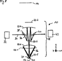
図1は、EUV投影露光装置の形態のマイクロリソグラフィ投影露光用の装置10の第1実施形態を座標系によるxz平面で示す断面図である。装置10は、図示のように、簡潔に「スキャナー」とも呼ばれるいわゆる「ステップ・アンド・スキャン露光装置」として設計してもよいし、またはいわゆる「ステッパー」として設計してもよい。
FIG. 1 is a cross-sectional view showing a first embodiment of an
装置10は、マスクパターン16を配置したマスク14にEUV波長領域の照明光線13(例えば13.4nmの波長を有する極紫外線)を入射させる照明システム12を備える。マスク14は、いわゆる「レチクルステージ」の形態のマスクテーブル11によって保持される。
The
さらに装置10は、基板平面19に配置した、ウェーハの形態の基板20の表面21にマスクパターン16を結像するための投影光学系の形態の光学系18を備える。装置10は、基板20を保持するいわゆる「ウェーハステージ」の形態の基板テーブル20aをさらに備える。上述のように図示の実施形態による装置は、いわゆる「スキャナー」として構成されている。基板20への視野の露光時に、マスクテーブル11および基板テーブル20aは、異なる速度で、図1に示した座標系によるy方向に変位される。
The
光学系18は、ミラーの形態の反射光学素子22のみを備える。したがって、光学系18は、「反射光学的投影対物レンズ」と呼ぶこともできる。基板20の表面21へのマスクパターン16の結像は、結像方向17aにマスクパターンを投影することによって行われる。結像方向17aは、図1ではz方向に延在する、光学系18における基準軸線17の方向に延在する。反射光学素子22が回転対称的である場合には、基準軸線17は光学系の光軸に対応する。
The
照明光線13は、マスク14によって結像光線15に変化させられる。結像光線15は、図1では見やすくするために輪郭のみを示す光学系18における結像光路24を通過する。図2は、結像光路24および結像光路に含まれる多数の個別光線を示す。光学系18における結像光線15の経路をさらに示すために、図3には、結像光線15の例示的な個別光線25が示されている。図3からわかるように、結像光線15は結像光路24で個別の反射光学系22−1〜22−6で順次に反射される。この場合、素子22−1および22−2はそれぞれ凹面鏡であり、素子22−3は凸面鏡であり、素子22−4は再び凹面鏡であり、素子22−5は凸面鏡、素子22−6は再び凹面鏡である。
The
光学系18は、反射光学素子22−3と反射光学素子22−4との間に配置された第1瞳平面28を備える。第1瞳平面28における結像光線15の光線横断面の中央領域には、「遮光絞り」とも呼ばれる遮光膜29が配置されている。遮光膜29は、視野とは無関係に瞳を遮光し、EUV波長領域における露光波長で光線を反射しない材料からなるか、またはそうような層を備える。この材料は、実質的にこの波長の入射光線を吸収する。
The
光路24に下流側に配置された反射光学素子22−5および22−6は、光学系18における開口率の高い部分に配置されており、それぞれの反射光学面27を通る中央孔の形態のそれぞれ1つの開口部26を有している。図5は、例示的な反射光学素子22におけるこのような開口部26を示している。図5に示すような開口部26は、反射光学素子22−5および22−6における、遮光膜29により少なくとも部分的に遮光された領域に配置されている。このような遮光膜29は、例えば国際公開第2006/069729号パンフレットに記載のように、照明光路24における高い光損失を防止するための役割を果たすことができる。
Reflective optical elements 22-5 and 22-6 arranged on the downstream side in the
さらに装置10は測定光線34を生成するための測定光線源32を備える。測定光線34は、結像光線15として別の波長、例えば可視波長領域の波長、特に、例えば632.8nm、UV波長領域、特にDUV波長領域、例えば248nm、VUV波長領域、例えば193nmまたは赤外線領域の波長を有していてもよい。測定光線34は、入射ミラーもしくは入射素子の形態の第1偏向ミラー38によって光学系18に入射させる。入射は、まず測定光路36が反射素子22−6における開口部26、次いで反射光学素子22−5における開口部26を通過して行われる。
The
次いで測定光線34は基板20の表面21で反射され、光学素子22−5および22−6における開口部26を再び通過する。この場合、測定光路36は、遮光膜29により遮光された領域で第1瞳平面28と共役の第2瞳平面30を2回通過する。測定光線34は、開口部26を再び通過した後に、射出ミラーもしくは射出素子の形態の第2偏向ミラー40によって検出器システム42に偏向される。測定光線34は、光学系18の一連の光学素子、特に光学素子22−1および22−2を通過することも、またこれらで反射されることもないので、光学系18を測定光線34は部分的にのみ通過する。
The measuring
検出器システム42によって、基板面21における1点以上において測定光線34が反射され、これらの点が結像方向17aにおける位置に関して測定される。このために、検出器システム42は、検出器および評価手段45を有し、検出手段45は、検出器が示した信号から基板表面21における1つまたは複数の測定点を決定する。図1に示した測定方向17aは、z座標軸に対して平行に延在しているので、一点のz座標または複数点のそれぞれのz座標を決定することができる。例えば米国特許出願公開第2007/0080281号公報に記載のように、このz座標の決定は、例えば反射された測定光線34と、光学系18を通過した測定光源32からの光線とを重ねることによって行われる。代替的に、米国特許第5268744号に記載の測定原理を用いることもでき、この測定原理では、基板表面21をz方向に変位することにより、検出器システム42の検出面における測定光線の入射場所が変位される。代替的には、反射された測定光線34を評価するためにドイツ国特許第4109484号明細書に記載の測定システムを使用することもできる。図4は、図1〜図3に示した結像光路24をyz平面で示す。測定光線34によって、基板表面21のトポグラフィー、ひいては基板表面21における複数点の相対位置を決定することもできる。
The
さらに、測定光線34は、基板表面21に配置した調整マークの側方位置を決定し、これにより、露光前に基板20を整列するために用いることができる。上述のように、このために調整マークを検出器システム42に直接に結像することができる。代替的に、測定光路36における、例えば基準ミラーに基準マークを付加的に配置してもよい。側方位置測定の可能性は、当業者には基本的に既知のモアレ測定法である。
Furthermore, the
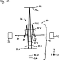
図6は、本発明による装置10の第2実施形態をxz平面における断面図で部分的に示す。図6に示す装置10は、測定光路36の構成のみが図1の装置10とは異なる。図6に示す測定光路36は、光学系18への入射後に測定光線34が第1偏向ミラー38によってまず反射性光学素子22−6で反射されるように構成されている。この場合、反射は反射性光学素子22−6の縁部領域23で行われる。この縁部領域23は、結像光路15の外部または内部に配置してもよく、縁部領域23は、結像光路15と部分的に重なっていてもよい。
FIG. 6 partially shows a second embodiment of the
縁部領域23で反射された測定光線34は、次いで反射素子22−5における開口部26を通過し、基板表面21で反射され、反射素子22−5における開口部26を再び通過し、反射性光学素子22−6の縁部領域23でもう一度反射される。この繰返しの反射は、第1の反射に関して光学系18の基準軸線17に対して反対側に位置する縁部領域23で行われる。次いで測定光線34は、第2偏向ミラー40を介して検出器システム42に偏向される。
The
図7、図8および図9は、本発明によるマイクロリソグラフィ投影露光用の装置10の第3実施形態を示す。より良好に図示するために、図7および図9には結像光路24のみを示し、図8には結像光路36のみを示す。図7および図8は、xz面における断面図で、図9はyz面における断面図で実施形態を示している。
7, 8 and 9 show a third embodiment of an
図7〜図9に示す光学系18は、上述の光学系18とは異なり、遮光膜29を備えていない。図9からわかるように、結像光路15は、反射光学素子22−1〜22−6の個別光学素子で、これら光学素子における反射前後に反射光学面を通過することなしにそれぞれ側方を案内される。反射光学素子22−1〜22−6は、前記実施形態とは異なり開口部26を備えていないものである。
Unlike the
図8に示すように、測定光路36は、測定光線34が反射光学素子22−1〜22−6で反射されるように、またはこれら反射光学素子を通過するように延在している。したがって、測定光線34はこの実施形態では反射光学素子22における開口部を通過しない。第1偏向ミラー38による光学系18への入射後に、測定光線34は凸面鏡の形態の光学素子22−3、同様に凸面鏡の形態の光学素子22−4、同様に凸面鏡の形態の光学素子22−5および同様に凸面鏡として構成された光学素子22−6で反射される。次いで測定光線34は基板表面21に入射し、第2偏向ミラー40によって検出器システム42で偏向されるまで、上記素子において反対の順序で反射されて光学系18を通過する。
As shown in FIG. 8, the measurement
図10は、例示的に示した露光領域43を有するウェーハの形態の基板20を平面図で示している。装置10を「スキャナー」として設計した場合、基板に入射した露光光線は、所定の時点でスリット状の面44を露光するように構成されている。このスリット状の面は、長方形またはリングセグメント状に構成されていてもよい。スキャン動作時には、基板20は不動の光学系18に対してy方向50にスキャンされる。これによりスリット状の露光面44は、反対方向52に効果的にスキャンされる。
FIG. 10 shows in plan view a
測定光路36は、装置10の上記実施形態全てにおいて3つの異なる変化態様で構成されていてもよい。第1変化態様では、測定光線34は、露光時点でスリット状の露光面44の内部の点または領域に向けられる。これにより、基板表面21の表面状態がスキャン工程の間に同時に測定される。第2変化態様では、測定光線34は露光面44における、基板29の先行する部分46に向けられる。第3変化態様では、測定光線34は、基板20における露光面44に後続する部分48に向けられる。
The measurement
装置10の本発明による別の実施形態では、基板表面21における点は基板20のスキャン動作中に結像方向17aに対して横方向の位置に関して2つの異なる時点で測定される。これにより、基板20のスキャン速度もしくは側方変位速度が決定される。
In another embodiment according to the invention of the
装置10の本発明による別の実施形態では、測定光線源32によって生成された測定光線34は少なくとも2つの異なる波長を有している。光線検出器42は、少なくとも2つの異なる波長に関して波長を解像し、基板表面21における反射後の測定光線34のそれぞれの強度を決定する。次いで光線強度から、基板表面21の温度が赤外線温度計の機能に類似した形で決定される。
In another embodiment of the
装置10の本発明による別の実施形態では、装置10の作動時に、光学系18を通過する測定光線34の強度低下が検出され、これにより、光学系18に含まれるガスの濃度が決定される。
In another embodiment according to the invention of the
図11は、マイクロリソグラフィ投影露光素位置10の本発明による別の実施形態を示す。この実施形態では、測定光路36は、装置10の作動時にマスク14における光学系18に向いた表面14aで測定光線34が反射されるように構成されている。これにより、例えばマスク表面14aにおける点の位置またはマスク表面14aのトポグラフィーを決定することもできる。基板20で測定光線34が反射される実施形態に関して上述した装置の他の特性を決定することもできる。
FIG. 11 shows another embodiment according to the invention of a microlithographic projection
図12は、基板20の表面を検査するための装置110の本発明による実施形態を示す。この装置110は、例えばリソグラフィマスクを検査するため、または露光されたウェーハを検査するための顕微鏡、または、光学検査システムである。装置は、マスク構造化システムを較正する、リソグラフィマスクにおける位置マークを高精度に測定するいわゆる「位置合わせ装置」として構成してもよい。このような測定により、リソグラフィマスクに配置され、ウェーハへの結像のために決定されたマスクパターンの書込み精度に関する結論を引き出すことができる。
FIG. 12 shows an embodiment according to the invention of an apparatus 110 for inspecting the surface of a
したがって、基板20は、半導体ウェーハ、リソグラフィマスクまたは一般に検査対象物である。装置110は、反対の結像方向17aに結像が行われる点においてだけ前述のマイクロリソグラフィ投影露光用の装置10とは異なっている。基板20は、かすめ入射した照明光線113によって照明される。基板20の表面21から放出した結像光線15は、光学系18の結像光路24を装置10の場合とは反対に通過する。表面21における検査すべき部分は、検出平面156に配置した検出手段154の検出面158に結像され、検出面154によって検出される。
Thus, the
装置110は、図1に示した測定光路36と類似に構成された測定光路36を備える。図2〜図5に示した構成は、対応して図12に示した実施形態における装置119に適用することができる。さらに、装置110は、図6〜図9に示した装置110に類似して構成してもよい。
The apparatus 110 includes a measurement
10 投影露光装置
11 マスクテーブル
12 照明システム
13 露光光線
14 マスク
14a 表面
15 結像光線
16 マスクパターン
17 基準軸線
17a 結像方向
18 光学系
19 基板平面
20 基板
20a 基板テーブル
21 基板表面
22−1〜22−6 反射光学素子
23 縁部領域
24 結像光路
25 結像光線の個別光線
26 開口部
27 光学面
28 第1瞳平面
29 遮光膜
30 第2瞳平面
32 測定光線源
34 測定光線
36 測定光路
38 第1偏向ミラー
40 第2偏向ミラー
42 検出器システム
43 露光領域
44 スリット状の露光面
45 評価手段
46 先行する部分
48 後続する部分
50 基板のスキャン方向
52 露光面の効果的なスキャン方向
110 検査装置
113 照明光線
154 検出手段
156 検出平面
158 検出面
DESCRIPTION OF
Claims (16)
結像光線(15)によってマスクパターン(16)を投影することにより基板(20)の表面(21)に前記マスクパターン(16)を結像するための光学系(18)であって、EUV波長領域および/または高周波数波長領域で作動するように構成された光学系と、
測定光線(34)を案内するための測定光路(36)であって、前記光学系(18)の少なくとも2つの光学素子(22)が前記測定光路(36)に含まれ、前記光学系(18)が、前記装置(10)の作動時に、前記測定光路に含まれない少なくとも一つの光学素子が存在するように、前記測定光線(34)によって部分的にのみ照射されるように、前記光学系(18)の内部に延在する測定光路(36)と
を備えることを特徴とする装置(10)。In an apparatus (10) for microlithographic projection exposure:
An optical system (18) for forming an image of the mask pattern (16) on the surface (21) of the substrate (20) by projecting the mask pattern (16) with an imaging light beam (15), the EUV wavelength An optical system configured to operate in the region and / or high frequency wavelength region;
A measurement optical path (36) for guiding a measurement light beam (34), wherein at least two optical elements (22) of the optical system (18) are included in the measurement optical path (36), and the optical system (18 ) Is only partially illuminated by the measuring beam (34) so that there is at least one optical element not included in the measuring beam path when the device (10) is activated. A measuring optical path (36) extending inside (18);
Device characterized in that it comprises (10).
前記測定光線(34)を前記光学系(18)に結合するために設けられた光学的な結合素子(38)をさらに備える装置。The apparatus of claim 1.
Apparatus further comprising an optical coupling element (38) provided for coupling the measuring beam (34) to the optical system (18).
前記光学系(18)から前記測定光線(34)を分離するための光学的な分離素子(40)をさらに備える装置。The apparatus according to claim 1 or 2,
The apparatus further comprising an optical separation element (40) for separating the measurement beam (34) from the optical system (18).
前記光学系(18)が少なくとも1つの反射光学素子(22)を備え、前記測定光路(36)が、前記装置(10)の作動時に少なくとも1つの反射光学素子(22−6;22−3,22−4,22−5,22−6)で前記測定光線(34)が反射されるように前記光学系(18)の内部に延在している装置。The device according to any one of claims 1 to 3,
The optical system (18) comprises at least one reflective optical element (22), and the measuring optical path (36) is at least one reflective optical element (22-6; 22-3, 22) when the device (10) is activated. 22-4, 22-5, 22-6) devices extending inside the optical system (18) so that the measuring beam (34) is reflected.
前記光学系(18)が少なくとも1つの反射光学素子(22)を備え、前記測定光路(36)が、前記装置(10)の作動時に前記測定光線(34)が少なくとも1つの反射光学素子(22−5,22−6)における開口(26)を通過するように前記光学系(18)の内部に延在している装置。The device according to any one of claims 1 to 4,
The optical system (18) comprises at least one reflective optical element (22), and the measuring light path (36) is such that when the device (10) is activated, the measuring beam (34) is at least one reflective optical element (22). A device extending inside the optical system (18) so as to pass through the aperture (26) in -5, 22-6).
前記光学系(18)が、反射光学系として構成されている装置。The device according to any one of claims 1 to 5,
An apparatus in which the optical system (18) is configured as a reflective optical system.
前記測定光路(36)が、前記装置(10;110)の作動時に、前記測定光路(36)を案内される前記測定光線(34)によって前記基板表面(21)の少なくとも1点をその位置に関して測定するように構成されている装置。The device according to any one of claims 1 to 6,
When the measuring beam path (36) is in operation of the device (10; 110), the measuring beam (34) guided along the measuring beam path (36) causes at least one point on the substrate surface (21) with respect to its position. A device that is configured to measure.
前記測定光路(36)が、前記装置(10;110)の作動時に前記測定光線(34)が前記基板(20)の表面(21)で反射されるように構成されている装置。The device according to any one of claims 1 to 7,
Apparatus wherein the measuring light path (36) is configured such that the measuring beam (34) is reflected by the surface (21) of the substrate (20) when the apparatus (10; 110) is activated.
少なくとも2つの異なる波長を有する前記測定光線(34)を生成する測定光線源(32)と、波長を分解する光線検出器(42)とを備え、該光線検出器が、前記基板(20)における反射後に前記測定光線(34)のそれぞれの強度を少なくとも2つの異なる波長それぞれについて測定し、これにより、前記基板表面(21)の温度を決定するように構成されている装置。The apparatus according to claim 8.
A measurement light source (32) for generating the measurement light beam (34) having at least two different wavelengths, and a light detector (42) for resolving the wavelength, the light detector in the substrate (20) An apparatus configured to measure the intensity of each of the measurement rays (34) after reflection for each of at least two different wavelengths, thereby determining the temperature of the substrate surface (21).
結像すべき前記マスクパターン(16)が前記マスク(14)に配置されており、前記測定光路(36)が、前記装置(10)の作動時に前記マスク(14)における前記光学系(18)に向いた前記表面(14a)で前記測定光線(34)が反射されるように構成されている装置。The device according to any one of claims 1 to 9,
The mask pattern (16) to be imaged is arranged on the mask (14), and the measuring optical path (36) is the optical system (18) in the mask (14) when the device (10) is activated. The apparatus is configured such that the measuring beam (34) is reflected by the surface (14a) facing towards.
前記結像方向(17a)に対して横方向に変位可能なマスクテーブル(11)と、制御手段とを備え、該制御手段が、前記マイクロリソグラフィ投影用の露光装置(10)を制御し、該装置(10)の作動時に、前記基板表面(21)における少なくとも1点が2つの異なる時点で前記結像方向(17a)に対して横方向の位置に関して測定されるように構成されており、前記装置(10)が、これにより、前記マスクテーブル(11)の側方変位速度を決定するように設定されている装置。The apparatus of claim 10.
A mask table (11) that can be displaced laterally with respect to the imaging direction (17a), and a control means, the control means controlling the exposure apparatus (10) for the microlithographic projection, During operation of the device (10), at least one point on the substrate surface (21) is measured at two different times with respect to a position transverse to the imaging direction (17a), The device (10) is thereby set to determine the lateral displacement speed of the mask table (11).
前記測定光路(36)が、前記光学系(18)の前記瞳平面(30)を少なくとも1回通って延在する装置。12. The device according to any one of claims 1 to 11,
Apparatus in which the measuring optical path (36) extends at least once through the pupil plane (30) of the optical system (18).
前記測定光路(36)が、前記測定光線(34)が少なくとも1つの前記反射光学素子(22−6;22−3,22−4,22−5,22−6)で2回反射されるように構成されている装置。The device according to any one of claims 4 to 12,
In the measurement optical path (36), the measurement light beam (34) is reflected twice by the at least one reflection optical element (22-6; 22-3, 22-4, 22-5, 22-6). A device that is configured to.
前記基板表面(21)へのマスクパターンの結像を行うと同時に、前記基板表面(21)における少なくとも1点の位置を決定するように構成されている装置。The device according to any one of claims 1 to 13,
An apparatus configured to determine the position of at least one point on the substrate surface (21) while simultaneously imaging a mask pattern on the substrate surface (21).
前記装置(10)が、EUV波長領域および/または高周波数波長領域の結像光線(15)によってマスクパターン(16)を投影することにより前記基板(20)の表面(21)に前記マスクパターン(16)を結像するための光学系(18)を備え、前記方法が、
前記光学系(18)の少なくとも2つの光学素子(22)が測定光路(36)に含まれ、前記光学系(18)が、前記測定光路に含まれない少なくとも一つの光学素子が存在するように、測定光線(34)によって部分的にのみ照射されるように、前記光学系(18)の内部で前記測定光線(34)を案内するステップと、
該測定光線(34)から前記システムの特性を決定するステップとを含むことを特徴とする方法。In a method for determining the characteristics of a system comprising an apparatus (10) for microlithographic projection exposure and a substrate (20) arranged at an exposure position of the apparatus (10),
The apparatus (10) projects the mask pattern (16) onto the surface (21) of the substrate (20) by projecting the mask pattern (16) with imaging light rays (15) in the EUV wavelength region and / or high frequency wavelength region. Comprising an optical system (18) for imaging 16), the method comprising:
At least two optical elements (22) of the optical system (18) are included in the measurement optical path (36), and the optical system (18) is present in at least one optical element not included in the measurement optical path. so as to be irradiated only in part by the measurement beam (34), the steps of guiding the measurement beam (34) within said optical system (18),
Determining the characteristics of the system from the measurement beam (34).
前記基板(20)の前記表面(21)における少なくとも2点で前記測定光線(34)を反射し、反射された前記測定光線(34)から、前記基板(20)の前記表面(21)における少なくとも一部のトポグラフィーを決定する方法。The method of claim 15, wherein
The measurement light beam (34) is reflected at at least two points on the surface (21) of the substrate (20), and from the reflected measurement light beam (34), at least on the surface (21) of the substrate (20). How to determine some topography.
Applications Claiming Priority (5)
| Application Number | Priority Date | Filing Date | Title |
|---|---|---|---|
| US7298008P | 2008-04-04 | 2008-04-04 | |
| US61/072,980 | 2008-04-04 | ||
| DE102008017645.1 | 2008-04-04 | ||
| DE102008017645A DE102008017645A1 (en) | 2008-04-04 | 2008-04-04 | Apparatus for microlithographic projection exposure and apparatus for inspecting a surface of a substrate |
| PCT/EP2009/002302 WO2009121541A1 (en) | 2008-04-04 | 2009-03-30 | Device for microlithographic projection illumination and device for the inspection of a surface of a substrate |
Related Child Applications (1)
| Application Number | Title | Priority Date | Filing Date |
|---|---|---|---|
| JP2011241389A Division JP5165101B2 (en) | 2008-04-04 | 2011-11-02 | Apparatus for microlithographic projection exposure and apparatus for inspecting the surface of a substrate |
Publications (2)
| Publication Number | Publication Date |
|---|---|
| JP2011517074A JP2011517074A (en) | 2011-05-26 |
| JP4892645B2 true JP4892645B2 (en) | 2012-03-07 |
Family
ID=41051533
Family Applications (2)
| Application Number | Title | Priority Date | Filing Date |
|---|---|---|---|
| JP2011502273A Expired - Fee Related JP4892645B2 (en) | 2008-04-04 | 2009-03-30 | Apparatus for microlithographic projection exposure and apparatus for inspecting the surface of a substrate |
| JP2011241389A Expired - Fee Related JP5165101B2 (en) | 2008-04-04 | 2011-11-02 | Apparatus for microlithographic projection exposure and apparatus for inspecting the surface of a substrate |
Family Applications After (1)
| Application Number | Title | Priority Date | Filing Date |
|---|---|---|---|
| JP2011241389A Expired - Fee Related JP5165101B2 (en) | 2008-04-04 | 2011-11-02 | Apparatus for microlithographic projection exposure and apparatus for inspecting the surface of a substrate |
Country Status (6)
| Country | Link |
|---|---|
| US (2) | US8345267B2 (en) |
| JP (2) | JP4892645B2 (en) |
| KR (1) | KR101633942B1 (en) |
| CN (2) | CN104122761B (en) |
| DE (1) | DE102008017645A1 (en) |
| WO (1) | WO2009121541A1 (en) |
Families Citing this family (14)
| Publication number | Priority date | Publication date | Assignee | Title |
|---|---|---|---|---|
| JP5022959B2 (en) * | 2008-03-24 | 2012-09-12 | 株式会社日立製作所 | Defect inspection system using catadioptric objective lens |
| DE102010041556A1 (en) | 2010-09-28 | 2012-03-29 | Carl Zeiss Smt Gmbh | Projection exposure apparatus for microlithography and method for microlithographic imaging |
| DE102010041562A1 (en) | 2010-09-28 | 2012-03-29 | Carl Zeiss Smt Gmbh | Projection exposure apparatus for microlithography and method for microlithographic exposure |
| WO2012137699A1 (en) * | 2011-04-05 | 2012-10-11 | 株式会社ニコン | Optical apparatus, exposure apparatus, and method of manufacturing device |
| US8903532B2 (en) * | 2012-03-26 | 2014-12-02 | Taiwan Semiconductor Manufacturing Co., Ltd. | Litho cluster and modulization to enhance productivity |
| US9196515B2 (en) | 2012-03-26 | 2015-11-24 | Taiwan Semiconductor Manufacturing Co., Ltd. | Litho cluster and modulization to enhance productivity |
| US8948495B2 (en) | 2012-08-01 | 2015-02-03 | Kla-Tencor Corp. | Inspecting a wafer and/or predicting one or more characteristics of a device being formed on a wafer |
| US8755114B1 (en) | 2013-06-14 | 2014-06-17 | Computer Power Supply, Inc. | Apparatus for aiding manual, mechanical alignment of optical equipment |
| CN103365118B (en) * | 2013-07-19 | 2015-03-25 | 中国科学院上海光学精密机械研究所 | Calibration method and calibration device for light beam monitoring system of mask aligner |
| US10495982B2 (en) * | 2013-10-28 | 2019-12-03 | Taiwan Semiconductor Manufacturing Company, Ltd. | System and method for real-time overlay error reduction |
| JP5932859B2 (en) * | 2014-02-18 | 2016-06-08 | キヤノン株式会社 | Detection apparatus, imprint apparatus, and article manufacturing method |
| WO2017136286A1 (en) | 2016-02-03 | 2017-08-10 | Kla-Tencor Corporation | Wafer defect inspection and review systems |
| US10656098B2 (en) | 2016-02-03 | 2020-05-19 | Kla-Tencor Corporation | Wafer defect inspection and review systems |
| DE102017217680A1 (en) * | 2017-10-05 | 2017-11-23 | Carl Zeiss Smt Gmbh | Projection objective with a measuring beam path |
Family Cites Families (63)
| Publication number | Priority date | Publication date | Assignee | Title |
|---|---|---|---|---|
| DE3318980C2 (en) | 1982-07-09 | 1986-09-18 | Perkin-Elmer Censor Anstalt, Vaduz | Device for adjustment during projection copying of masks |
| NL8600639A (en) | 1986-03-12 | 1987-10-01 | Asm Lithography Bv | METHOD FOR ALIGNING A MASK AND A SUBSTRATE AND DEVICE FOR CARRYING OUT THE METHOD |
| US4747678A (en) * | 1986-12-17 | 1988-05-31 | The Perkin-Elmer Corporation | Optical relay system with magnification |
| NL8900991A (en) * | 1989-04-20 | 1990-11-16 | Asm Lithography Bv | DEVICE FOR IMAGING A MASK PATTERN ON A SUBSTRATE. |
| JP2890882B2 (en) | 1990-04-06 | 1999-05-17 | キヤノン株式会社 | Positioning method, semiconductor device manufacturing method, and projection exposure apparatus using the same |
| DE4109484C2 (en) | 1991-03-22 | 2001-03-01 | Zeiss Carl Fa | Measuring lens |
| JP3384038B2 (en) * | 1992-06-15 | 2003-03-10 | 株式会社ニコン | Surface position detection optical device |
| US5978071A (en) | 1993-01-07 | 1999-11-02 | Nikon Corporation | Projection exposure apparatus and method in which mask stage is moved to provide alignment with a moving wafer stage |
| JP3412704B2 (en) * | 1993-02-26 | 2003-06-03 | 株式会社ニコン | Projection exposure method and apparatus, and exposure apparatus |
| JP3368091B2 (en) | 1994-04-22 | 2003-01-20 | キヤノン株式会社 | Projection exposure apparatus and device manufacturing method |
| US5825043A (en) * | 1996-10-07 | 1998-10-20 | Nikon Precision Inc. | Focusing and tilting adjustment system for lithography aligner, manufacturing apparatus or inspection apparatus |
| JPH10209039A (en) | 1997-01-27 | 1998-08-07 | Nikon Corp | Method and apparatus for projection exposure |
| JP4037947B2 (en) * | 1998-01-29 | 2008-01-23 | 株式会社テクノホロン | Object alignment method |
| WO1999040613A1 (en) | 1998-02-09 | 1999-08-12 | Nikon Corporation | Method of adjusting position detector |
| US6240158B1 (en) * | 1998-02-17 | 2001-05-29 | Nikon Corporation | X-ray projection exposure apparatus with a position detection optical system |
| JPH11238666A (en) * | 1998-02-19 | 1999-08-31 | Nikon Corp | X-ray projection aligner |
| WO2000019497A1 (en) * | 1998-09-30 | 2000-04-06 | Nikon Corporation | Alignment method and method for producing device using the alignment method |
| CN1309017C (en) * | 1998-11-18 | 2007-04-04 | 株式会社尼康 | Exposure method and device |
| US6241056B1 (en) * | 1998-12-29 | 2001-06-05 | Hayes Lemmerz International, Inc. | Composite brake drum |
| JP3796369B2 (en) | 1999-03-24 | 2006-07-12 | キヤノン株式会社 | Projection exposure system with interferometer |
| JP4175748B2 (en) * | 1999-09-20 | 2008-11-05 | 大日本スクリーン製造株式会社 | Pattern inspection device |
| JP2001185480A (en) * | 1999-10-15 | 2001-07-06 | Nikon Corp | Optical projection system and projection exposure device equipped with the system |
| EP1093021A3 (en) * | 1999-10-15 | 2004-06-30 | Nikon Corporation | Projection optical system as well as equipment and methods making use of said system |
| US6600608B1 (en) * | 1999-11-05 | 2003-07-29 | Carl-Zeiss-Stiftung | Catadioptric objective comprising two intermediate images |
| JP2002175964A (en) * | 2000-12-06 | 2002-06-21 | Nikon Corp | Observation system and method of manufacturing the same, aligner, and method of manufacturing microdevice |
| WO2002084406A1 (en) | 2001-04-17 | 2002-10-24 | Koninklijke Philips Electronics N.V. | Euv-transparent interface structure |
| DE10120446C2 (en) | 2001-04-26 | 2003-04-17 | Zeiss Carl | Projection exposure system and method for compensating imaging errors in a projection exposure system, in particular for micro-lithography |
| DE10139177A1 (en) * | 2001-08-16 | 2003-02-27 | Zeiss Carl | Objective with pupil obscuration |
| US6618120B2 (en) * | 2001-10-11 | 2003-09-09 | Nikon Corporation | Devices and methods for compensating for tilting of a leveling table in a microlithography apparatus |
| TWI225665B (en) * | 2001-10-17 | 2004-12-21 | Canon Kk | Apparatus control system, apparatus control method, semiconductor exposure apparatus, semiconductor exposure apparatus control method and semiconductor device manufacturing method |
| JP3564104B2 (en) * | 2002-01-29 | 2004-09-08 | キヤノン株式会社 | Exposure apparatus, control method therefor, and device manufacturing method using the same |
| US7092069B2 (en) * | 2002-03-08 | 2006-08-15 | Carl Zeiss Smt Ag | Projection exposure method and projection exposure system |
| DE10220816A1 (en) * | 2002-05-10 | 2003-11-20 | Zeiss Carl Microelectronic Sys | Reflective X-ray microscope for examining an object in an object plane illuminates the object with beam wavelengths less than 30 nm while scanning it into an image plane as an enlarged object |
| US6828542B2 (en) | 2002-06-07 | 2004-12-07 | Brion Technologies, Inc. | System and method for lithography process monitoring and control |
| US20030234993A1 (en) | 2002-06-21 | 2003-12-25 | Hazelton Andrew J. | Adaptive optic off-axis metrology |
| US7362508B2 (en) | 2002-08-23 | 2008-04-22 | Nikon Corporation | Projection optical system and method for photolithography and exposure apparatus and method using same |
| WO2004021086A1 (en) | 2002-08-26 | 2004-03-11 | Carl Zeiss Smt Ag | Grating based spectral filter for eliminating out of band radiation in an extreme ultra-violet lithography system |
| EP1394616A1 (en) | 2002-08-29 | 2004-03-03 | ASML Netherlands BV | An alignment tool, a lithographic apparatus, an alignment method and a device manufacturing method |
| JP2004193269A (en) * | 2002-12-10 | 2004-07-08 | Hitachi Ltd | Manufacturing method of mask, and manufacturing method of semiconductor integrated circuit device |
| TWI242692B (en) | 2002-12-16 | 2005-11-01 | Asml Netherlands Bv | Lithographic apparatus, device manufacturing method, and device manufactured thereby |
| JP2004228456A (en) | 2003-01-27 | 2004-08-12 | Canon Inc | Exposure device |
| DE10323664B4 (en) | 2003-05-14 | 2006-02-16 | Carl Zeiss Smt Ag | Exposure device with dose sensors |
| JP4378109B2 (en) * | 2003-05-30 | 2009-12-02 | キヤノン株式会社 | Exposure apparatus, projection optical system, and device manufacturing method |
| AU2003304304A1 (en) | 2003-07-05 | 2005-01-21 | Carl Zeiss Smt Ag | Device for the polarization-specific examination of an optical system |
| EP1496398A1 (en) | 2003-07-05 | 2005-01-12 | Carl Zeiss SMT AG | Apparatus for polarisation related inspection, optical projection system and calibration method |
| JP2005166785A (en) | 2003-12-01 | 2005-06-23 | Canon Inc | Device and method for detecting position and aligner |
| US7288779B2 (en) * | 2003-12-17 | 2007-10-30 | Asml Netherlands B.V. | Method for position determination, method for overlay optimization, and lithographic projection apparatus |
| US20050134816A1 (en) * | 2003-12-22 | 2005-06-23 | Asml Netherlands B.V. | Lithographic apparatus, method of exposing a substrate, method of measurement, device manufacturing method, and device manufactured thereby |
| CN102169226B (en) | 2004-01-14 | 2014-04-23 | 卡尔蔡司Smt有限责任公司 | Catadioptric projection objective |
| JP2005209896A (en) * | 2004-01-23 | 2005-08-04 | Nikon Corp | Method for detecting reticle position in euv exposure apparatus |
| JP4843272B2 (en) * | 2004-07-31 | 2011-12-21 | カール・ツァイス・エスエムティー・ゲーエムベーハー | Optical system for microlithographic projection exposure apparatus |
| KR101148589B1 (en) | 2004-12-23 | 2012-05-22 | 칼 짜이스 에스엠티 게엠베하 | High aperture lens with an obscured pupil |
| DE102005042005A1 (en) | 2004-12-23 | 2006-07-06 | Carl Zeiss Smt Ag | Objective lens esp. as micro-lithography projection objective, has objective divided into first part-objective with single mirror and second part-objective with primary and secondary mirror |
| EP1856142B1 (en) | 2004-12-30 | 2009-08-12 | F. Hoffmann-Roche AG | Synthesis of peptide t-1249 using peptide intermediate fragments |
| US7282701B2 (en) | 2005-02-28 | 2007-10-16 | Asml Netherlands B.V. | Sensor for use in a lithographic apparatus |
| US7612892B2 (en) | 2005-10-06 | 2009-11-03 | Nikon Corporation | Imaging optical system configured with through the lens optics for producing control information |
| JP5622068B2 (en) | 2005-11-15 | 2014-11-12 | 株式会社ニコン | Surface position detection apparatus, exposure apparatus, and device manufacturing method |
| DE102005056914A1 (en) | 2005-11-29 | 2007-05-31 | Carl Zeiss Smt Ag | Projection illumination system for use with production of e.g. integrated circuit, has interferometer arrangement examining optical components by measuring radiation that strikes on optical surface at specific angle of incidence |
| DE102005062618B4 (en) * | 2005-12-23 | 2008-05-08 | Carl Zeiss Smt Ag | Optical imaging device and imaging method with determination of aberrations |
| JP4924604B2 (en) | 2006-03-10 | 2012-04-25 | 株式会社ニコン | Projection optical system, exposure apparatus, and semiconductor device manufacturing method |
| JP2007250947A (en) * | 2006-03-17 | 2007-09-27 | Canon Inc | Exposure apparatus and image surface detecting method |
| JP2008108852A (en) * | 2006-10-24 | 2008-05-08 | Canon Inc | Projection exposure apparatus, optical component, and method of manufacturing device |
| EP1950594A1 (en) * | 2007-01-17 | 2008-07-30 | Carl Zeiss SMT AG | Imaging optical system, projection illumination unit for microlithography with such an optical system, method for manufacturing a microstructured component with such a projection illumination unit, microstructured component produced by the manufacturing method and use of such an optical system |
-
2008
- 2008-04-04 DE DE102008017645A patent/DE102008017645A1/en not_active Ceased
-
2009
- 2009-03-30 CN CN201410363267.7A patent/CN104122761B/en not_active Expired - Fee Related
- 2009-03-30 CN CN200980119381.2A patent/CN102124411B/en not_active Expired - Fee Related
- 2009-03-30 JP JP2011502273A patent/JP4892645B2/en not_active Expired - Fee Related
- 2009-03-30 WO PCT/EP2009/002302 patent/WO2009121541A1/en active Application Filing
- 2009-03-30 KR KR1020107024702A patent/KR101633942B1/en active IP Right Grant
-
2010
- 2010-09-30 US US12/895,747 patent/US8345267B2/en active Active
-
2011
- 2011-11-02 JP JP2011241389A patent/JP5165101B2/en not_active Expired - Fee Related
-
2012
- 2012-10-25 US US13/660,327 patent/US8953173B2/en not_active Expired - Fee Related
Also Published As
| Publication number | Publication date |
|---|---|
| DE102008017645A1 (en) | 2009-10-08 |
| JP5165101B2 (en) | 2013-03-21 |
| KR101633942B1 (en) | 2016-06-27 |
| JP2012089852A (en) | 2012-05-10 |
| CN102124411A (en) | 2011-07-13 |
| CN104122761B (en) | 2017-11-14 |
| US8953173B2 (en) | 2015-02-10 |
| CN102124411B (en) | 2014-08-27 |
| JP2011517074A (en) | 2011-05-26 |
| WO2009121541A1 (en) | 2009-10-08 |
| CN104122761A (en) | 2014-10-29 |
| KR20100125476A (en) | 2010-11-30 |
| US20130050672A1 (en) | 2013-02-28 |
| US8345267B2 (en) | 2013-01-01 |
| US20110085179A1 (en) | 2011-04-14 |
Similar Documents
| Publication | Publication Date | Title |
|---|---|---|
| JP4892645B2 (en) | Apparatus for microlithographic projection exposure and apparatus for inspecting the surface of a substrate | |
| US20190129318A1 (en) | Projection exposure system for microlithography with a measurement device | |
| JP5406624B2 (en) | Detection apparatus, exposure apparatus, and device manufacturing method | |
| JP6004126B1 (en) | Inspection device and focus adjustment method thereof | |
| KR101267144B1 (en) | Sensor calibration method, exposure method, exposure device, device fabrication method, and reflection type mask | |
| JP6006919B2 (en) | Catadioptric lighting system for metrology | |
| JPH0810124B2 (en) | Exposure equipment | |
| EP3108299A1 (en) | An imaging system in reflection mode using coherent diffraction imaging methods and using micro-pinhole and aperture system | |
| JPH11251226A (en) | X-ray projection aligner | |
| US5838450A (en) | Direct reticle to wafer alignment using fluorescence for integrated circuit lithography | |
| JP4729463B2 (en) | Exposure apparatus, particle inspection system, particle inspection method, and device manufacturing method | |
| JP2007288186A (en) | Lithographic apparatus, lens interferometer, and device manufacturing method | |
| JP2006245030A (en) | Measurement method and object with measurement pattern | |
| JP2535889B2 (en) | Projection optical device | |
| TWI815479B (en) | Method and apparatus for characterization of a microlithography mask | |
| JPH0744138B2 (en) | Alignment device | |
| JPH10172900A (en) | Exposure apparatus | |
| JP2004165218A (en) | Aligner | |
| JP2005266622A (en) | Mask defect inspection apparatus | |
| JPS5974625A (en) | Projection type exposure device | |
| JP4765313B2 (en) | Exposure equipment | |
| JPH10289871A (en) | Projection exposure device | |
| JP2004264127A (en) | Mark position detector | |
| KR101368601B1 (en) | Optical imaging device with determination of imaging errors | |
| WO2012041458A2 (en) | Projection exposure tool for microlithography and method for microlithographic exposure |
Legal Events
| Date | Code | Title | Description |
|---|---|---|---|
| A131 | Notification of reasons for refusal |
Free format text: JAPANESE INTERMEDIATE CODE: A131 Effective date: 20110308 |
|
| A521 | Request for written amendment filed |
Free format text: JAPANESE INTERMEDIATE CODE: A523 Effective date: 20110607 |
|
| A02 | Decision of refusal |
Free format text: JAPANESE INTERMEDIATE CODE: A02 Effective date: 20110705 |
|
| A521 | Request for written amendment filed |
Free format text: JAPANESE INTERMEDIATE CODE: A523 Effective date: 20111102 |
|
| A911 | Transfer to examiner for re-examination before appeal (zenchi) |
Free format text: JAPANESE INTERMEDIATE CODE: A911 Effective date: 20111111 |
|
| TRDD | Decision of grant or rejection written | ||
| A01 | Written decision to grant a patent or to grant a registration (utility model) |
Free format text: JAPANESE INTERMEDIATE CODE: A01 Effective date: 20111206 |
|
| A01 | Written decision to grant a patent or to grant a registration (utility model) |
Free format text: JAPANESE INTERMEDIATE CODE: A01 |
|
| A61 | First payment of annual fees (during grant procedure) |
Free format text: JAPANESE INTERMEDIATE CODE: A61 Effective date: 20111219 |
|
| R150 | Certificate of patent or registration of utility model |
Ref document number: 4892645 Country of ref document: JP Free format text: JAPANESE INTERMEDIATE CODE: R150 Free format text: JAPANESE INTERMEDIATE CODE: R150 |
|
| FPAY | Renewal fee payment (event date is renewal date of database) |
Free format text: PAYMENT UNTIL: 20141222 Year of fee payment: 3 |
|
| R250 | Receipt of annual fees |
Free format text: JAPANESE INTERMEDIATE CODE: R250 |
|
| R250 | Receipt of annual fees |
Free format text: JAPANESE INTERMEDIATE CODE: R250 |
|
| R250 | Receipt of annual fees |
Free format text: JAPANESE INTERMEDIATE CODE: R250 |
|
| R250 | Receipt of annual fees |
Free format text: JAPANESE INTERMEDIATE CODE: R250 |
|
| R250 | Receipt of annual fees |
Free format text: JAPANESE INTERMEDIATE CODE: R250 |
|
| R250 | Receipt of annual fees |
Free format text: JAPANESE INTERMEDIATE CODE: R250 |
|
| R250 | Receipt of annual fees |
Free format text: JAPANESE INTERMEDIATE CODE: R250 |
|
| R250 | Receipt of annual fees |
Free format text: JAPANESE INTERMEDIATE CODE: R250 |
|
| LAPS | Cancellation because of no payment of annual fees |