JP4880994B2 - Recording head and recording apparatus - Google Patents
Recording head and recording apparatus Download PDFInfo
- Publication number
- JP4880994B2 JP4880994B2 JP2005372521A JP2005372521A JP4880994B2 JP 4880994 B2 JP4880994 B2 JP 4880994B2 JP 2005372521 A JP2005372521 A JP 2005372521A JP 2005372521 A JP2005372521 A JP 2005372521A JP 4880994 B2 JP4880994 B2 JP 4880994B2
- Authority
- JP
- Japan
- Prior art keywords
- recording
- recording elements
- delay
- time
- signal
- Prior art date
- Legal status (The legal status is an assumption and is not a legal conclusion. Google has not performed a legal analysis and makes no representation as to the accuracy of the status listed.)
- Active
Links
Images


Classifications
-
- B—PERFORMING OPERATIONS; TRANSPORTING
- B41—PRINTING; LINING MACHINES; TYPEWRITERS; STAMPS
- B41J—TYPEWRITERS; SELECTIVE PRINTING MECHANISMS, i.e. MECHANISMS PRINTING OTHERWISE THAN FROM A FORME; CORRECTION OF TYPOGRAPHICAL ERRORS
- B41J2/00—Typewriters or selective printing mechanisms characterised by the printing or marking process for which they are designed
- B41J2/005—Typewriters or selective printing mechanisms characterised by the printing or marking process for which they are designed characterised by bringing liquid or particles selectively into contact with a printing material
- B41J2/01—Ink jet
- B41J2/015—Ink jet characterised by the jet generation process
- B41J2/04—Ink jet characterised by the jet generation process generating single droplets or particles on demand
- B41J2/045—Ink jet characterised by the jet generation process generating single droplets or particles on demand by pressure, e.g. electromechanical transducers
- B41J2/04501—Control methods or devices therefor, e.g. driver circuits, control circuits
- B41J2/04591—Width of the driving signal being adjusted
-
- B—PERFORMING OPERATIONS; TRANSPORTING
- B41—PRINTING; LINING MACHINES; TYPEWRITERS; STAMPS
- B41J—TYPEWRITERS; SELECTIVE PRINTING MECHANISMS, i.e. MECHANISMS PRINTING OTHERWISE THAN FROM A FORME; CORRECTION OF TYPOGRAPHICAL ERRORS
- B41J2/00—Typewriters or selective printing mechanisms characterised by the printing or marking process for which they are designed
- B41J2/005—Typewriters or selective printing mechanisms characterised by the printing or marking process for which they are designed characterised by bringing liquid or particles selectively into contact with a printing material
- B41J2/01—Ink jet
- B41J2/015—Ink jet characterised by the jet generation process
- B41J2/04—Ink jet characterised by the jet generation process generating single droplets or particles on demand
- B41J2/045—Ink jet characterised by the jet generation process generating single droplets or particles on demand by pressure, e.g. electromechanical transducers
- B41J2/04501—Control methods or devices therefor, e.g. driver circuits, control circuits
- B41J2/04528—Control methods or devices therefor, e.g. driver circuits, control circuits aiming at warming up the head
-
- B—PERFORMING OPERATIONS; TRANSPORTING
- B41—PRINTING; LINING MACHINES; TYPEWRITERS; STAMPS
- B41J—TYPEWRITERS; SELECTIVE PRINTING MECHANISMS, i.e. MECHANISMS PRINTING OTHERWISE THAN FROM A FORME; CORRECTION OF TYPOGRAPHICAL ERRORS
- B41J2/00—Typewriters or selective printing mechanisms characterised by the printing or marking process for which they are designed
- B41J2/005—Typewriters or selective printing mechanisms characterised by the printing or marking process for which they are designed characterised by bringing liquid or particles selectively into contact with a printing material
- B41J2/01—Ink jet
- B41J2/015—Ink jet characterised by the jet generation process
- B41J2/04—Ink jet characterised by the jet generation process generating single droplets or particles on demand
- B41J2/045—Ink jet characterised by the jet generation process generating single droplets or particles on demand by pressure, e.g. electromechanical transducers
- B41J2/04501—Control methods or devices therefor, e.g. driver circuits, control circuits
- B41J2/04541—Specific driving circuit
-
- B—PERFORMING OPERATIONS; TRANSPORTING
- B41—PRINTING; LINING MACHINES; TYPEWRITERS; STAMPS
- B41J—TYPEWRITERS; SELECTIVE PRINTING MECHANISMS, i.e. MECHANISMS PRINTING OTHERWISE THAN FROM A FORME; CORRECTION OF TYPOGRAPHICAL ERRORS
- B41J2/00—Typewriters or selective printing mechanisms characterised by the printing or marking process for which they are designed
- B41J2/005—Typewriters or selective printing mechanisms characterised by the printing or marking process for which they are designed characterised by bringing liquid or particles selectively into contact with a printing material
- B41J2/01—Ink jet
- B41J2/015—Ink jet characterised by the jet generation process
- B41J2/04—Ink jet characterised by the jet generation process generating single droplets or particles on demand
- B41J2/045—Ink jet characterised by the jet generation process generating single droplets or particles on demand by pressure, e.g. electromechanical transducers
- B41J2/04501—Control methods or devices therefor, e.g. driver circuits, control circuits
- B41J2/04543—Block driving
-
- B—PERFORMING OPERATIONS; TRANSPORTING
- B41—PRINTING; LINING MACHINES; TYPEWRITERS; STAMPS
- B41J—TYPEWRITERS; SELECTIVE PRINTING MECHANISMS, i.e. MECHANISMS PRINTING OTHERWISE THAN FROM A FORME; CORRECTION OF TYPOGRAPHICAL ERRORS
- B41J2/00—Typewriters or selective printing mechanisms characterised by the printing or marking process for which they are designed
- B41J2/005—Typewriters or selective printing mechanisms characterised by the printing or marking process for which they are designed characterised by bringing liquid or particles selectively into contact with a printing material
- B41J2/01—Ink jet
- B41J2/015—Ink jet characterised by the jet generation process
- B41J2/04—Ink jet characterised by the jet generation process generating single droplets or particles on demand
- B41J2/045—Ink jet characterised by the jet generation process generating single droplets or particles on demand by pressure, e.g. electromechanical transducers
- B41J2/04501—Control methods or devices therefor, e.g. driver circuits, control circuits
- B41J2/04553—Control methods or devices therefor, e.g. driver circuits, control circuits detecting ambient temperature
-
- B—PERFORMING OPERATIONS; TRANSPORTING
- B41—PRINTING; LINING MACHINES; TYPEWRITERS; STAMPS
- B41J—TYPEWRITERS; SELECTIVE PRINTING MECHANISMS, i.e. MECHANISMS PRINTING OTHERWISE THAN FROM A FORME; CORRECTION OF TYPOGRAPHICAL ERRORS
- B41J2/00—Typewriters or selective printing mechanisms characterised by the printing or marking process for which they are designed
- B41J2/005—Typewriters or selective printing mechanisms characterised by the printing or marking process for which they are designed characterised by bringing liquid or particles selectively into contact with a printing material
- B41J2/01—Ink jet
- B41J2/015—Ink jet characterised by the jet generation process
- B41J2/04—Ink jet characterised by the jet generation process generating single droplets or particles on demand
- B41J2/045—Ink jet characterised by the jet generation process generating single droplets or particles on demand by pressure, e.g. electromechanical transducers
- B41J2/04501—Control methods or devices therefor, e.g. driver circuits, control circuits
- B41J2/04573—Timing; Delays
-
- B—PERFORMING OPERATIONS; TRANSPORTING
- B41—PRINTING; LINING MACHINES; TYPEWRITERS; STAMPS
- B41J—TYPEWRITERS; SELECTIVE PRINTING MECHANISMS, i.e. MECHANISMS PRINTING OTHERWISE THAN FROM A FORME; CORRECTION OF TYPOGRAPHICAL ERRORS
- B41J2/00—Typewriters or selective printing mechanisms characterised by the printing or marking process for which they are designed
- B41J2/005—Typewriters or selective printing mechanisms characterised by the printing or marking process for which they are designed characterised by bringing liquid or particles selectively into contact with a printing material
- B41J2/01—Ink jet
- B41J2/015—Ink jet characterised by the jet generation process
- B41J2/04—Ink jet characterised by the jet generation process generating single droplets or particles on demand
- B41J2/045—Ink jet characterised by the jet generation process generating single droplets or particles on demand by pressure, e.g. electromechanical transducers
- B41J2/04501—Control methods or devices therefor, e.g. driver circuits, control circuits
- B41J2/0458—Control methods or devices therefor, e.g. driver circuits, control circuits controlling heads based on heating elements forming bubbles
-
- B—PERFORMING OPERATIONS; TRANSPORTING
- B41—PRINTING; LINING MACHINES; TYPEWRITERS; STAMPS
- B41J—TYPEWRITERS; SELECTIVE PRINTING MECHANISMS, i.e. MECHANISMS PRINTING OTHERWISE THAN FROM A FORME; CORRECTION OF TYPOGRAPHICAL ERRORS
- B41J2/00—Typewriters or selective printing mechanisms characterised by the printing or marking process for which they are designed
- B41J2/005—Typewriters or selective printing mechanisms characterised by the printing or marking process for which they are designed characterised by bringing liquid or particles selectively into contact with a printing material
- B41J2/01—Ink jet
- B41J2/015—Ink jet characterised by the jet generation process
- B41J2/04—Ink jet characterised by the jet generation process generating single droplets or particles on demand
- B41J2/045—Ink jet characterised by the jet generation process generating single droplets or particles on demand by pressure, e.g. electromechanical transducers
- B41J2/04501—Control methods or devices therefor, e.g. driver circuits, control circuits
- B41J2/04581—Control methods or devices therefor, e.g. driver circuits, control circuits controlling heads based on piezoelectric elements
Description
本発明は、安定したプリントを行い得る記録ヘッドおよびこの記録ヘッドを用いて記録を行う記録装置に関するものである。 The present invention relates to a recording head that can perform stable printing and a recording apparatus that performs recording using the recording head.
従来から、複数個の記録素子を一列、もしくは複数列に配置してなる記録ヘッドが種々知られている。この種の記録ヘッドは、記録素子N個を1ブロックとして同時駆動可能な駆動用集積回路を同一基板上に数個または数十個搭載している。そして画像データを各記録素子に対応させて整列させることにより、紙等の被記録材に任意の記録を行わせている。これらのヘッドとして吐出口からインクを吐出するための吐出エネルギーを発生する電気熱変換素子を記録素子として複数個配列したヘッドが知られている。このような記録ヘッドでは、記録素子を駆動するための電力が大きなものになる等の理由で記録素子を複数のブロックに分割し、ブロック毎に順次または分散駆動する方法が知られている。 Conventionally, various recording heads in which a plurality of recording elements are arranged in one or a plurality of rows are known. This type of recording head has several or several tens of driving integrated circuits mounted on the same substrate that can be driven simultaneously with N recording elements as one block. The image data is aligned in correspondence with each recording element, whereby arbitrary recording is performed on a recording material such as paper. As these heads, there are known heads in which a plurality of electrothermal conversion elements that generate ejection energy for ejecting ink from ejection ports are arranged as recording elements. In such a recording head, there is known a method in which the recording element is divided into a plurality of blocks for the reason that the power for driving the recording elements becomes large, and the blocks are sequentially or distributedly driven for each block.
また電力の点だけでなく一つの記録素子が連続して駆動されると熱が蓄積され、記録濃度の変化を生じる可能性がある。また、記録素子はこれに隣接する記録素子からもその熱の影響を受ける。また、インクジェット記録装置においては隣接する記録素子を同時に駆動すると、インク吐出の際に生じる圧力により、各々のノズルに相互的な圧力による干渉を受ける。この圧力干渉(クロストーク)により、記録濃度の変化を生じる場合がある。このために記録素子を駆動した後に、ある程度放熱もしくはクロストークを避ける休止時間を設けることが望ましい。 Further, not only in terms of electric power but also when one recording element is driven continuously, heat is accumulated and there is a possibility that a change in recording density occurs. The recording element is also affected by the heat from the recording element adjacent thereto. In the ink jet recording apparatus, when adjacent recording elements are driven simultaneously, the pressure generated when ink is ejected causes each nozzle to receive interference due to mutual pressure. This pressure interference (crosstalk) may cause a change in recording density. For this reason, it is desirable to provide a pause time to avoid heat dissipation or crosstalk to some extent after driving the recording element.
以上のような点に関して同時駆動する記録素子を列方向に対して分散させる分散駆動が知られている。この駆動方法によれば隣接した記録素子が同時に駆動することがない為、休止時間を設けることによって隣接記録素子からの影響を排除することを可能にしている。その具体的な例として、同時駆動可能な記録素子の全てに共通に接続された複数のイネーブル端子により分散駆動を実現している。図7に従来の記録ヘッドの記録素子駆動回路を示す。 Dispersion driving is known in which the recording elements that are simultaneously driven with respect to the above points are dispersed in the column direction. According to this driving method, adjacent recording elements are not driven at the same time. Therefore, it is possible to eliminate the influence from the adjacent recording elements by providing a pause time. As a specific example, distributed driving is realized by a plurality of enable terminals commonly connected to all of the simultaneously driven recording elements. FIG. 7 shows a recording element driving circuit of a conventional recording head.
従来型の回路の駆動方法としては、クロック端子CLKより画像データ転送クロックを、データ信号端子DATAより画像データをシフトレジスタ8に転送する。画像データをラッチ11にラッチするために、ラッチ端子LATより信号入力し、各記録素子に対応して画像データを整列させれば、ラッチパルス信号の周期分、画像データに合わせて記録素子への通電がブロック毎に可能となる。時分割駆動する単位となるブロック選択は、ENB_0、ENB_1、ENB_2、ENB_3のオン・オフの組み合わせがデコーダにより16ブロックにデコードされることでなされる。ラッチパルスの周期の範囲内で、ブロックを順次選択していきこのブロックの範囲内でヒートイネーブル端子HEAT_1、HEAT_2より駆動パルス信号を16ブロック分数入力することにより、時分割分散駆動を達成できる。記録素子に与える駆動パルス信号の幅は、高分解能な制御ができるように機能素子(ドライバ)3の立上がり立下り時間を高速にしている。
しかしながら、上記構成の記録ヘッドにおいて記録ヘッドの高速化、高精細カラー化、記録ヘッドデバイスの小型化を達成する場合には次のような課題を生じる場合がある。同時駆動する記録素子数により、配線において記録電流集中による問題が生じることがある。これは駆動パルス信号の立上がり、立下り時のスイッチングノイズに基づく誤動作である。例えば機能素子10の立上がり立下り時間tを100ナノ秒、配線の自己インダクタンスLを100ナノヘンリー、その時に流れる集中電流を1アンペアとすると、
V=L・di/dt
=100×10−9×1/100×10−9
=1〔V〕
となり、1ボルトもの誘導電圧がノイズとして生じることになる。このノイズレベルはCMOSもしくはTTL等の論理ゲート回路部においてかなりの影響を与えるものである。特に3.3ボルト以下のCMOS論理ロジックの場合、スレッショルドレベルに達するほどのレベルである。このように、大電流をスイッチングする機能素子10を有する制御ブロックと、シフトレジスタやラッチを構成するCMOSもしくはTTL等の論理ゲート回路部が同居しているような記録ヘッドデバイスでは誤動作を引き起こす場合がある。
However, in the recording head having the above-described configuration, the following problems may occur when achieving high-speed recording, high-definition color, and miniaturization of the recording head device. Depending on the number of recording elements that are driven simultaneously, a problem may occur due to concentration of recording current in the wiring. This is a malfunction based on switching noise at the rise and fall of the drive pulse signal. For example, if the rise / fall time t of the
V = L · di / dt
= 100 × 10 −9 × 1/100 × 10 −9
= 1 [V]
Thus, an induced voltage of 1 volt is generated as noise. This noise level has a considerable influence on a logic gate circuit such as CMOS or TTL. In particular, in the case of CMOS logic logic of 3.3 volts or less, the level is such that the threshold level is reached. As described above, in a recording head device in which a control block having the
記録ヘッドの高速化、高精細化を計ると記録素子数の増加に伴い、分割駆動させるブロック数の増加、及び同時駆動させる素子数が増加することが考えられる。しかし高速化という点からブロック数の増加には限界があるため、同時駆動する素子数を増やす方向の要請が強まる傾向にあり、記録電流集中の値も大きくなりノイズレベルが高くなることになる。 If the recording head is increased in speed and definition, it is conceivable that the number of blocks to be divided and the number of elements to be simultaneously driven increase as the number of recording elements increases. However, since the increase in the number of blocks is limited from the viewpoint of speeding up, there is a tendency to increase the number of simultaneously driven elements, and the value of the recording current concentration increases and the noise level increases.
従来からこのような同時駆動時のスイッチングノイズは問題になっており、そのための対策がいくつか知られている。例えば同じブロックとして駆動する記録素子へ与える駆動制御パルス信号を段階的に遅らせる方法がある。この方法の場合、スイッチングノイズのレベルと幅を考慮し、駆動パルス信号を記録素子に印加するタイミングを段階的に遅らせる遅延素子をパルス幅規定信号のする構成としている。しかしながらこの方法は、1つのブロックの駆動期間内における駆動数がさらに増加したときには次のような課題がある。通常、駆動周期内(1記録素子を連続して駆動する周期)に全ての記録素子を駆動できるようにパルス幅許容時間を割り当てる。しかしこのために十分な遅延時間が取れず、スイッチングノイズの影響を防止することが困難になってしまう。 Conventionally, such switching noise at the time of simultaneous driving has been a problem, and several countermeasures for this are known. For example, there is a method of delaying the drive control pulse signal given to the recording elements driven as the same block in a stepwise manner. In the case of this method, in consideration of the level and width of switching noise, the delay element that delays the timing of applying the drive pulse signal to the recording element stepwise is used as the pulse width defining signal. However, this method has the following problems when the number of drives in the drive period of one block further increases. Usually, an allowable pulse width time is assigned so that all the recording elements can be driven within the driving period (period in which one recording element is continuously driven). However, sufficient delay time cannot be taken for this reason, and it becomes difficult to prevent the influence of switching noise.
本発明は上記の事情を鑑みてそれを解決するためになされたものである。記録素子に与える駆動パルス信号を段階的に遅らせるだけでなく、時分割ブロック信号をも段階的に遅らせる。このことで、記録素子を同じブロック内で駆動させる際に発生するスイッチングノイズの影響を防止する記録ヘッドを提供することを目的とするものである。 This invention is made | formed in order to solve it in view of said situation. Not only is the drive pulse signal applied to the recording element delayed in stages, but the time division block signal is also delayed in stages. Accordingly, it is an object of the present invention to provide a recording head that prevents the influence of switching noise generated when the recording elements are driven in the same block.
上述の課題である記録素子の増大、及び高速駆動を行う際に、記録素子同時駆動時に生じるスイッチングノイズに記録制御部が影響されないように、本発明の記録ヘッドは以下の構成を備える。 The recording head of the present invention has the following configuration so that the recording control unit is not affected by switching noise generated during simultaneous driving of the recording elements when increasing the number of recording elements and performing high-speed driving, which are the problems described above.
複数の記録素子と、前記記録素子に対応して夫々設けられ前記記録素子を通電する複数のドライバと、前記記録素子に通電するパルスの時間幅を規定するためのパルス幅規定信号を入力する入力手段と、前記複数の記録素子を隣り合う所定数の記録素子ごとに複数のブロックに分割し、各ブロックに含まれる記録素子を異なるタイミングで通電するための時分割制御信号を生成する生成手段とを有する記録ヘッドにおいて、前記入力手段から入力されたパルス幅規定信号を前記複数のドライバへ供給するための第1の共通配線において隣り合うブロックの間に対応する位置に配置され、前記パルス幅規定信号を遅延させる第1の遅延手段と、前記生成手段で生成された複数の時分割信号を前記複数のドライバへ転送するための第2の共通配線において隣り合うブロックの間に対応する位置に配置され、前記時分割制御信号を遅延させる第2の遅延手段と、を有することを特徴とする。 A plurality of recording elements, a plurality of drivers respectively provided corresponding to the recording elements and energizing the recording elements, and an input for inputting a pulse width defining signal for defining a time width of a pulse energizing the recording elements And means for generating a time-division control signal for dividing the plurality of recording elements into a plurality of blocks for each predetermined number of adjacent recording elements and energizing the recording elements included in each block at different timings; In the first common wiring for supplying the pulse width defining signal input from the input means to the plurality of drivers, the recording head having the pulse width defining position. First delay means for delaying a signal, and second common wiring for transferring a plurality of time division signals generated by the generation means to the plurality of drivers Hey are disposed at corresponding positions between the adjacent blocks, and having a second delay means for delaying said time division control signal.
また、上記ヘッドと制御手段を有する装置である。 Moreover, it is an apparatus having the head and control means.
本発明の構成により高速プリントに不可欠である記録素子の増大や高密度実装に伴う同時駆動される発熱体数の増加に対しても、発生するノイズの画像データ制御ラインへの影響を低減する。このことで、安定した記録を実現することができる。 The configuration of the present invention reduces the influence of generated noise on the image data control line even when the number of recording elements, which are indispensable for high-speed printing, and the number of heating elements driven simultaneously with high-density mounting are increased. As a result, stable recording can be realized.
以下、添付の図面を参照して本発明の好適な実施形態を説明する。 Hereinafter, preferred embodiments of the present invention will be described with reference to the accompanying drawings.
[本発明を適用可能な記録装置の説明]
図10は、本発明が適用できるインクジェット記録装置の概観図である。同図において、キャリッジHCは、リードスクリュー5004の螺旋溝5005に対して係合するピン(不図示)を有し、リードスクリュー5004の回転に伴って矢印a,b方向に往復移動される。このキャリッジHCには、インクジェットカートリッジIJCが搭載されている。インクジェットカートリッジIJCは、インクジェットヘッドIJH(以下、ヘッドユニットという)及び記録用のインクを貯蔵するインクタンクITを具備する。
[Description of recording apparatus to which the present invention is applicable]
FIG. 10 is a schematic view of an ink jet recording apparatus to which the present invention can be applied. In the drawing, the carriage HC has a pin (not shown) that engages with a spiral groove 5005 of the
5002は紙押え板であり、キャリッジの移動方向に亙って紙をプラテン5000に対して押圧する。プラテン5000は不図示の搬送モータにより回転し、記録紙Pを搬送する。5016は記録ヘッドの前面をキャップするキャップ部材5022を支持する部材である。これらのキャッピング、クリーニング、吸引回復は、キャリッジがホームポジション側の領域に来た時にリードスクリュー5004の作用によって処理が行えるように構成されている。しかし、周知のタイミングで所望の作動を行うようにすれば、本例にはいずれも適用できる。
次に、上述した装置の記録制御を実行するための制御構成について、図2に示すブロック図を参照して説明する。制御回路を示す同図において、1700は記録信号を入力するインターフェース、1701はMPU、1702はMPU1701が実行する制御プログラムを格納するプログラムROMである。また、1703は各種データ(上記記録信号やヘッドに供給される記録データ等)を保存しておくダイナミック型のRAM(以下、DRAM)である。1704は記録ヘッド1708に対する記録データやヘッド駆動のための信号の供給制御を行うゲートアレイであり、インターフェース1700、MPU1701、RAM1703間のデータ転送制御も行う。以上は本体側制御部101が有する構成である。
Next, a control configuration for executing the recording control of the above-described apparatus will be described with reference to a block diagram shown in FIG. In the figure, showing a control circuit, 1700 is an interface for inputting a recording signal, 1701 is an MPU, and 1702 is a program ROM for storing a control program executed by the MPU 1701.
1709は記録紙Pを搬送するための搬送モータ(図10では不図示)である。1706は搬送モータ1709を駆動するためのモータドライバ、1707はキャリッジモータ5013を駆動するためのモータドライバである。
上記制御構成の動作を説明すると、インターフェース1700に記録信号が入るとゲートアレイ1704とMPU1701との間で記録信号がプリント用の記録データに変換される。そして、モータドライバ1706、1707が駆動されると共に、キャリッジHCに送られた記録データに従ってインクジェットヘッドIJHが駆動され、記録紙P上への画像記録が行われる。
The operation of the control configuration will be described. When a recording signal enters the
なお、インクジェットヘッドIJHの記録素子部を駆動するに際して、最適な駆動を行なうために、ヘッドユニット103内のメモリに保持されている特性情報が参照され、各記録素子の駆動形態が決定される。また、以下の説明では、インクジェットヘッドIJHを記録ヘッドと称する。
Note that when driving the recording element portion of the ink jet head IJH, in order to perform optimal driving, the characteristic information held in the memory in the
[第1の実施形態]
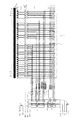
図11は本発明を適用可能な記録ヘッドの構成を特徴的な部分のみ模式的に示した図である。構成例として、本発明の一実施例としてインクジェット記録ヘッド用基板1に、複数の記録用素子(図ではseg.0からseg.255まで256個・1列)2を設けた例である。記録用素子上に構造的に設けられたインク吐出ノズル(図示せず)にインクを供給するインク供給口14をこの基板に対して異方性エッチング、もしくはサンドブラスト等の処理によって形成したものである。インク供給口14に対し、一列(数ノズル単位で段違いに配列することも可)に電気熱変換体(抵抗体)で構成された記録用の素子(記録素子)列2を配置する。記録素子は後で説明するが、記録画像データにあわせて選択的に駆動されるよう制御回路に接続されている。更に記録素子列2を個別に駆動制御するMOS−FET等の機能素子(ドライバ)列3とその個別制御を可能にする回路配線9が続いて配置される。電源供給用共通電極(VH)4、電源接地用共通電極(GNDH)5は前記記録素子列や機能素子列を挟むように配置してもよい。機能素子と多層になるように配置してもよい。インクジェット記録ヘッドの構成に合わせて共通電極を配置することが可能である。
[First Embodiment]
FIG. 11 is a diagram schematically showing only the characteristic part of the configuration of the recording head to which the present invention is applicable. As an example of the configuration, as an embodiment of the present invention, an ink jet
近年の基板は上記記録素子列だけでなく、ドライバ列のような機能素子群やその制御回路まで内蔵して構成するものが多く、記録装置全体のコスト低減に貢献している。その中で数百ノズルにもわたる記録素子列を個別制御するために重要な役割を果たすのがシフトレジスタ回路10、ラッチ回路11等である。記録素子が増加した場合でも、制御端子数を記録素子数に合わせて増やす必要がないため、この回路の組み合わせで構成された制御回路を有するインクジェット記録ヘッド用基板が主流になりつつある。インクジェット記録ヘッドの場合、前述のようにインク流によるクロストークという現象が生ずる。吐出ノズルから吐出されるインク滴はクロストークにより不安定になることがある。このため、隣接する記録素子を同時に駆動しないよう、分離して制御できるようになっている。これらはHEAT_1、HEAT_2という端子に通電信号(パルス幅規定信号)を加えることで制御が可能である。前述のラッチ回路11による記録素子個別制御信号と上記通電信号と、さらに時分割駆動信号とのAND出力によって記録素子を駆動する。時分割制御信号端子ENB_0(1,2,3)からの時分割制御信号は記録ヘッドの駆動ブロックに対応して設定されている。時分割の方法、選択回路、配線の構成は多岐にわたるものであり、本構成に限るものではない。符号9で示される枠内の15は遅延回路であり、遅延回路1つにつき所定の時間の信号遅延を生じさせる。時分割駆動信号線BLOCK内の15も同じく遅延回路である。遅延回路の接続数が増せばそれに比例して遅延時間も増す。ローバスフィルター或いはバッファより構成される遅延回路15の例を図5(a)(b)に示す。遅延時間は、同時駆動する記録素子の駆動電流や記録素子の電流の立上がり・立下がり時間に応じて設定されるが、おおよそ数ns〜数10ns程度である。必要な遅延時間を生じさせる回路の構成は多岐にわたり、特に本構成に限るものではない。番号で示さない部分は、インクジェット記録ヘッド用基板に記録電流を通電したり、記録の制御を行うための制御端子パッドである。7の時分割駆動回路等から延長して配線される複数の制御系列配線は、カラー化に対応した場合でも共通に使用されることがあるため、インクジェット記録ヘッド用基板1の表面を這い巡らす形で敷設される。
In recent years, not only the above-described recording element array, but also many functional elements such as a driver array and its control circuit are built in, and this contributes to cost reduction of the entire recording apparatus. Among them, the
図8は図11の記録ヘッド回路構成における駆動タイミングチャートの例である。インクジェット記録ヘッドのノズル列画像データとして展開された後は、そのデータをDATA端子へ入力する。このデータ信号は基本的にシリアルデータであり、シフトレジスタ回路10に供給され、本構成では記録素子256個分の幅でそのデータをラッチ回路11に一時的に保持する。保持するためのラッチクロックに相当するのがLAT端子である。このデータは次のデータが入力されるまで保持されている。256個の記録素子は16個ずつの16ブロックに分けられ、このブロック単位で時分割駆動をなされている。ENB_0、ENB_1、ENB_2、ENB_3は時分割駆動を行うための時分割制御信号の端子であり、この4信号のハイ・ローの入力を図9のようにデコードした出力BLOCK_nで16ブロックの選択を行う。ラッチ回路でデータが保持されている間に16ブロックを順次選択する(図示せず)。そして、前述の記録素子を通電制御するHEAT_1、HEAT_2の通電信号を入力する。そして画像データにあわせて記録素子の選択がなされ、その通電信号(パルス幅規定信号)が規定するパルス幅にて記録電流が記録素子に通電される。HEAT_1、HEAT_2を図のようにシフトして印加することで、パルス幅を入力するトータル時間をデータ転送クロック送信時間の範囲内で短くすることができる。これはインク吐出の周期を少しでも短くし、記録装置の高速化につなげるひとつの手段である。このように図11の回路の範囲で、記録ヘッドを駆動するタイミングチャートをいくつか設定することができる。記録装置の印刷モード等に合わせて時間を設定することが可能である。
FIG. 8 is an example of a drive timing chart in the printhead circuit configuration of FIG. After being developed as nozzle row image data of the ink jet recording head, the data is input to the DATA terminal. This data signal is basically serial data and is supplied to the
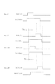
図1は図11の記録ヘッド回路構成における各記録素子に入力される信号の例である。遅延回路の動作の例である。本構成では、seg.0からseg.15までは遅延は入らず、seg.16からseg.31までに1段の遅延が、seg.32からseg.47までは2段の遅延が、順次1段ずつ遅延が増えていく。seg.224からseg.255では15段の遅延が入るように設定されている。遅延の段数の異なる各記録素子へのブロック信号を、mをブロック信号線の番号とし、nを遅延の段数として、BLOCK_m_nとする。また、遅延の段数の異なる各記録素子へ与える通電信号を、nを遅延の段数として、HEAT_1_n、HEAT_2_nとする。 FIG. 1 is an example of a signal input to each recording element in the recording head circuit configuration of FIG. It is an example of operation | movement of a delay circuit. In this configuration, seg. 0 to seg. No delay until 15 and seg. 16 to seg. 1 stage delay until 31, seg. 32 to seg. Up to 47, the delay is two stages, and the delay is sequentially increased by one stage. seg. 224 to seg. In 255, a delay of 15 stages is set. A block signal to each recording element having a different number of delay stages is BLOCK_m_n, where m is a block signal line number and n is the number of delay stages. In addition, energization signals to be applied to the recording elements having different numbers of delay stages are HEAT_1_n and HEAT_2_n, where n is the number of delay stages.
図6では、BLOCK_0が共通で遅延の段数のみ異なるという点で、seg.0+16n(nは遅延の段数)について特に図示している。HEAT_1、HEAT_2はパルス幅がBLOCK_0の間に入るようタイミングをずらして入力される。遅延が一段入るごとに遅延時間tDLずつ遅延するため、BLOCK_0_0では遅延はないが、BLOCK_0_7ではtDLの7倍、BLOCK_0_15ではtDLの15倍、BLOCK_0_0から遅延している。 In FIG. 6, seg. Is different in that BLOCK_0 is common and only the number of delay stages is different. Specifically, 0 + 16n (n is the number of delay stages) is illustrated. HEAT_1 and HEAT_2 are input at different timings so that the pulse width falls between BLOCK_0. To delay by the delay time t DL whenever the delay enters stage, there is no delay in BLOCK_0_0, 7 times t DL in BLOCK_0_7, 15 times the t DL in BLOCK_0_15, it is delayed from BLOCK_0_0.
同様に、seg.0のHEAT_1_0ではHEAT_1から遅延はないが、seg.112のHEAT_2_7ではtDLの7倍、seg.240のHEAT_2_15ではtDLの15倍、HEAT_2から遅延している。したがって、どのノズルにおいてもHEAT_1、HEAT_2がBLOCK_0内に収まっており、十分な遅延時間を取ることが可能である。BLOCK_0及びSMALLに遅延が入っていない場合は、次のようになるそれはDATA_1_15とBLOCK_0_0(SMALL_0)を比較して明らかなように、DATA_1_15がBLOCK_0_0(SMALL_0)からはみ出してしまう。これではseg.226には十分なエネルギーが与えられず、記録素子を駆動することは不可能である。 Similarly, seg. 0 HEAT_1_0 has no delay from HEAT_1, but seg. 7 times the HEAT_2_7 in t DL of 112, seg. 15 times the HEAT_2_15 in t DL of 240, has been delayed from HEAT_2. Therefore, HEAT_1 and HEAT_2 are contained in BLOCK_0 in any nozzle, and a sufficient delay time can be taken. When there is no delay in BLOCK_0 and SMALL, it becomes as follows. As is apparent from comparing DATA_1_15 and BLOCK_0_0 (SMALL_0), DATA_1_15 protrudes from BLOCK_0_0 (SMALL_0). With this, seg. Sufficient energy is not given to 226, and it is impossible to drive the recording element.
なお、本構成では1つの記録素子におけるBLOCKとHEAT_1(HEAT_2)の遅延の段数は常に同一にしている。 In this configuration, the number of delay stages of BLOCK and HEAT_1 (HEAT_2) in one printing element is always the same.
しかしそもそもBLOCKの幅はHEAT信号のパルス幅よりマージンをもって広く設定していることが一般的である。したがって、HEAT_1(HEAT_2)がBLOCKの内に収まるのであれば、BLOCKの遅延の段数を少なくする構成であっても良い。例えば、HEAT_1(HEAT_2)の遅延が2段入るごとに1段遅延を入れるといった構成が考えられ、BLOCK信号線上の遅延回路を削減できるというメリットが得られる。 However, in general, the width of BLOCK is generally set wider with a margin than the pulse width of the HEAT signal. Therefore, as long as HEAT_1 (HEAT_2) is within BLOCK, the number of delay stages of BLOCK may be reduced. For example, a configuration in which a one-stage delay is inserted every two delays of HEAT_1 (HEAT_2) can be conceived, and an advantage is obtained that the delay circuit on the BLOCK signal line can be reduced.
以上説明により、時分割駆動を行うブロック選択部に遅延回路を設けたことにより、十分な遅延時間を取りスイッチングノイズの影響を防止することが可能である。 As described above, by providing a delay circuit in the block selection unit that performs time-division driving, it is possible to take a sufficient delay time and prevent the influence of switching noise.
なお、本発明は上記構成のようなサーマルインクジェットヘッドに限らない。つまり、所定の記録素子数からなるブロックを単位として時分割駆動を行い、同一ブロック内で同時駆動する記録素子に対して遅延をもたせて駆動する記録ヘッドであれば、どのような記録ヘッドであっても良い。インクジェットでないサーマルヘッドや圧電素子で吐出するタイプのインクジェットヘッドであっても上記の条件を満たしていれば本発明は適用可能である。 The present invention is not limited to the thermal ink jet head having the above configuration. In other words, any recording head can be used as long as the recording head performs time-division driving in units of blocks each having a predetermined number of recording elements and drives the recording elements that are simultaneously driven in the same block with a delay. May be. The present invention can be applied to a thermal head that is not an ink jet or an ink jet head that is ejected by a piezoelectric element as long as the above conditions are satisfied.
[第2の実施形態]
図3は本発明を適用可能な記録ヘッドの構成を特徴的な部分のみ模式的に示した図である。図11と異なる構成について以下に説明する。6は7の時分割駆動信号系列配線を出力配線とするブロック選択のための制御回路で、記録素子群を32ノズルずつのブロックに分け選択し時分割駆動するための回路である。通常デコーダ回路やシフトレジスタ回路で構成されるものである。8は記録素子に記録電流を通電する駆動パルスの通電時間設定用AND回路列である。本実施例の構成においては、隣接する記録素子のヒータ抵抗値とノズル形状を変えることにより、異なるサイズのインク吐出量を実現している。このような大小ヒータを交互に配置しているため、大小をひとつのペアとして駆動制御している。前述のクロストークを考慮した駆動制御は、このペアをひとつとした回路構成となっている。これらはHEAT_1、HEAT_2という端子に通電信号を加えることで制御が可能である。前述のラッチ回路11による記録素子個別制御信号とHEAT_1、HEAT_2信号のAND出力が9の個別制御回路配線およびAND回路列となる。このAND回路の出力を決定するのが、6で示す時分割駆動用デコーダ回路の出力である時分割駆動信号系列配線7である。これらの信号は記録ヘッドの駆動ブロックに対応して設定されており、時分割の方法、選択回路、配線の構成は多岐にわたるものであり、本構成に限るものではない。7及び8内の15は遅延回路であり、遅延回路1つにつき所定の時間の信号遅延を生じさせる。番号で示さない部分は、インクジェット記録ヘッド用基板に記録電流を通電したり、記録制御を行うための制御端子パッドである。7の時分割駆動回路等から延長して配線される複数の制御系列配線は、カラー化に対応した場合でも共通に使用されることがあるため、インクジェット記録ヘッド用基板1の表面を這い巡らす形で敷設される。
[Second Embodiment]
FIG. 3 is a diagram schematically showing only the characteristic part of the configuration of the recording head to which the present invention is applicable. A configuration different from FIG. 11 will be described below. Reference numeral 6 denotes a control circuit for block selection using the time-division drive signal series wiring of 7 as an output wiring, and is a circuit for selecting and recording the recording element group into blocks each having 32 nozzles. Usually, it is composed of a decoder circuit and a shift register circuit.
インクジェット記録ヘッドは、電流を流すことで記録ヘッド基板自体の温度は上昇するが、低温度環境では、インクの温度、ヘッド基板の温度ともに低く、すぐにインクの吐出を開始すると本来のインクの吐出性能を出せないことが多い。そのためヘッド基板を加熱制御し、常温環境と同等にするための基板加熱用サブヒータ12を具備する。12は記録素子と同様の材質で作り込まれた抵抗素子が一般的である。更に環境温度を検知するための基板温度センサ13を併設する。同一基板に設置するために、基板上に作りこむことが可能なアルミニウム抵抗素子やダイオード等の素子を用いることが多い。これら温度調節制御のための素子は、記録ヘッド基板に直接取り付ける方法でも同様な効果は得られる。ヘッド基板に接するインクの温度や基板温度を直接検知する精度を必要とする場合、同一基板上に作り込むのが最適な構成といえる。
記録ヘッドに温度調節制御部品を取り付ける必要がないので、記録ヘッドコストの低減が可能である。
Ink jet print heads raise the temperature of the print head substrate itself by passing an electric current, but in a low temperature environment, both the ink temperature and the head substrate temperature are low. In many cases, performance cannot be achieved. For this purpose, a sub-heater 12 for heating the substrate is provided to control the heating of the head substrate so as to make it equivalent to a room temperature environment. A resistor element 12 is generally made of the same material as the recording element. Furthermore, a substrate temperature sensor 13 for detecting the environmental temperature is also provided. In order to install on the same substrate, an element such as an aluminum resistance element or a diode that can be formed on the substrate is often used. These elements for temperature adjustment control can obtain the same effect even if they are directly attached to the recording head substrate. When the accuracy of directly detecting the temperature of the ink in contact with the head substrate or the substrate temperature is required, it can be said that the optimum configuration is to make it on the same substrate.
Since there is no need to attach a temperature adjustment control component to the recording head, the recording head cost can be reduced.
図4は図3の記録ヘッド回路構成における駆動タイミングチャートの例である。インクジェット記録ヘッドのノズル列画像データとして展開された後は、そのデータをDATA端子へ入力する。このデータ信号は基本的にシリアルデータであり、シフトレジスタ回路10に供給され、適当な分割幅でそのデータをラッチ回路11に一時的に保持する。保持するためのラッチクロックに相当するのがLAT端子である。このデータは次のデータが入力されるまで保持されているので、その間に前述の記録素子を通電制御するHEAT_1、HEAT_2信号を入力すれば、画像データにあわせて記録素子の記録通電が選択的になされるというものである。近年では記録ヘッドへの端子数を低減するため、時分割駆動設定データもDATA端子に画像データとともにシリアル転送する方法が知られている。駆動タイミングチャートの一部を拡大説明した図の例は、16個の記録素子個別制御データと時分割駆動するブロック番号を設定するデータである。更に諧調選択として大小何れかのヒータを駆動する選択データまで、本DATA端子に入力することが可能なものである。この駆動タイミングによれば、16×22=64ノズル分の駆動が大小何れかの画像データ選択により駆動できる。時分割設定データと同時に必要な記録素子の個別制御データをセットできるので、64ノズル分のシフトレジスタ、ラッチ回路を必要としない点は、記録ヘッド基板サイズの低減に大きく貢献する。また時分割駆動制御に対応するシリアルデータビットを追加すれば2のべき乗でブロックを増加させることができるので、本構成のデータ転送は記録素子の増加に柔軟に対応できる。このためこのデータをラッチした後、HEAT信号を印加すれば、そのパルス幅にて記録電流が記録素子に通電される。HEAT_1、HEAT_2を図のようにシフトして印加することで、パルス幅を入力するトータル時間をデータ転送クロック送信時間の範囲内で短くすることができる。これはインク吐出の周期を少しでも短くし、記録装置の高速化につなげるひとつの手段である。このように図3の回路の範囲で、記録ヘッドを駆動するタイミングチャートをいくつか設定することができる。記録装置の印刷モード等に合わせて時間を設定することが可能である。
FIG. 4 is an example of a drive timing chart in the printhead circuit configuration of FIG. After being developed as nozzle row image data of the ink jet recording head, the data is input to the DATA terminal. This data signal is basically serial data and is supplied to the
図6は図3の記録ヘッド回路構成における各記録素子に入力される信号の例である。遅延回路の動作の例である。本構成では、seg.0からseg.15までは遅延は入らず、seg.16からseg.31までに1段の遅延入る。また、seg.32からseg.47までは2段の遅延が、順次1段ずつ遅延が増えていき、seg.224からseg.255では15段の遅延が入るように設定されている。遅延の段数の異なる各記録素子へのブロック信号を、mをブロック信号線の番号とし、nを遅延の段数として、BLOCK_m_nとする。また、遅延の段数の異なる各記録素子への大小選択信号を、nを遅延の段数として、LARGE_n(SMALL_n)とする。また、HEAT_1、HEAT_2とノズル選択のDATA信号のANDを取ったものを、nを遅延の段数として、DATA_1_n、DATA_2_nとする。図6では、BLOCK_0とSMALLが共通で遅延の段数のみ異なるという点で、seg.0+16n,seg.2+16n(nは遅延の段数)について特に図示している。BLOCK_0とSMALLはラッチクロックが入力されるまで常に保持されており、HEAT_1、HEAT_2はパルス幅がこの間に入るようタイミングをずらして入力される。HEAT_1(HEAT_2)とDATA_1_0(DATA_2_0)のタイミングは等しいが、遅延が一段入るごとに遅延時間tDLずつ遅延する。このためDATA_1_7ではtDLの7倍、DATA_1_15ではtDLの15倍、HEAT_1から遅延している。 FIG. 6 is an example of signals input to each recording element in the recording head circuit configuration of FIG. It is an example of operation | movement of a delay circuit. In this configuration, seg. 0 to seg. No delay until 15 and seg. 16 to seg. A delay of one stage is entered by 31. Also, seg. 32 to seg. Up to 47, the delay is two stages, and the delay gradually increases by one stage. 224 to seg. In 255, a delay of 15 stages is set. A block signal to each recording element having a different number of delay stages is BLOCK_m_n, where m is a block signal line number and n is the number of delay stages. Also, the size selection signal to each recording element having a different number of delay stages is set to LARGE_n (SMALL_n), where n is the number of delay stages. Further, the AND of the HEAT_1 and HEAT_2 and the nozzle selection DATA signal is defined as DATA_1_n and DATA_2_n, where n is the number of delay stages. In FIG. 6, BLOCK_0 and SMALL are common and differ only in the number of delay stages. 0 + 16n, seg. Specifically, 2 + 16n (n is the number of delay stages) is illustrated. BLOCK_0 and SMALL are always held until the latch clock is input, and HEAT_1 and HEAT_2 are input at different timings so that the pulse width falls between them. Equal timing HEAT_1 (HEAT_2) and DATA_1_0 (DATA_2_0), but delayed by a delay time t DL whenever the delay enters stage. 7 times this for DATA_1_7 At t DL, 15 times the t DL in DATA_1_15, are delayed from HEAT_1.
これと同様に、BLOCK_0_0(SMALL_0)では遅延はなく、BLOCK_0_7(SMALL_7)ではtDLの7倍、BLOCK_0_15(SMALL_15)ではtDLの15倍、BLOCK_0_0から遅延はない。そして、どのノズルにおいてもDATA1、DATA2がBLOCK_0(SMALL)内に収まっており、十分な遅延時間を取ることが可能である。BLOCK_0及びSMALLに遅延が入っていない場合は、DATA_1_15とBLOCK_0_0(SMALL_0)を比較して明らかなように、DATA_1_15がBLOCK_0_0(SMALL_0)からはみ出してしまう。これではseg.226には十分なエネルギーが与えられず、記録素子を駆動することは不可能である。 Similarly, BLOCK_0_0 (SMALL_0) in no delay, BLOCK_0_7 (SMALL_7) 7 times at t DL, BLOCK_0_15 (SMALL_15) 15 times the t DL, there is no delay from BLOCK_0_0. In any nozzle, DATA1 and DATA2 are within BLOCK_0 (SMALL), and a sufficient delay time can be taken. When there is no delay in BLOCK_0 and SMALL, DATA_1_15 protrudes from BLOCK_0_0 (SMALL_0), as is clear by comparing DATA_1_15 and BLOCK_0_0 (SMALL_0). With this, seg. Sufficient energy is not given to 226, and it is impossible to drive the recording element.
なお、本構成では1つの記録素子におけるBLOCKとDATA_1(DATA_2)の遅延の段数は常に同一にしている。しかし、そもそもBLOCKの幅はHEAT信号のパルス幅よりマージンをもって広く設定していることが一般的である。そこで、DATA_1(DATA_2)がBLOCKの内に収まるのであれば、BLOCKの遅延の段数を少なくする構成であっても良い。 In this configuration, the number of delay stages of BLOCK and DATA_1 (DATA_2) in one recording element is always the same. However, in general, the width of BLOCK is generally set wider with a margin than the pulse width of the HEAT signal. Therefore, as long as DATA_1 (DATA_2) is within BLOCK, the number of BLOCK delay stages may be reduced.
例えば、DATA_1(DATA_2)の遅延が2段入るごとに1段遅延を入れるといった構成が考えられ、BLOCK信号線上の遅延回路を削減できるというメリットが得られる。 For example, a configuration in which a delay of one stage is inserted every two delays of DATA_1 (DATA_2) can be considered, and an advantage that a delay circuit on the BLOCK signal line can be reduced is obtained.
以上説明により、時分割駆動を行うブロック選択部及び大小の諧調選択部に遅延回路を設けたことにより、十分な遅延時間を取りスイッチングノイズの影響を防止することが可能である。 As described above, by providing the delay circuit in the block selection unit that performs time-division driving and the large and small gradation selection unit, it is possible to take sufficient delay time and prevent the influence of switching noise.
以上説明したように、本発明の記録ヘッドによれば、記録素子、ブロック選択部、駆動パルス幅入力部、駆動パルス信号のタイミングをずらす遅延回路と共に、ブロック選択部にも遅延回路を設けた構成とする。このことで、高速プリントに不可欠な吐出口数の増大などに伴う同時駆動する発熱体数の増加に対しても、ノイズが画像データ制御ラインに与える影響を防止することが可能で、安定した動作を実現できる。 As described above, according to the recording head of the present invention, the recording element, the block selection unit, the drive pulse width input unit, the delay circuit for shifting the timing of the drive pulse signal, and the delay circuit also provided in the block selection unit And This makes it possible to prevent the influence of noise on the image data control line even when the number of heating elements that are driven simultaneously with the increase in the number of ejection ports, which is indispensable for high-speed printing, is stable. realizable.
1 記録ヘッド用基板
2 記録素子列
3 ドライバ列
4 電源供給用共通電極
5 電源接地用共通電極
6 分割駆動回路
7 分割駆動系列配線
8 通電時間設定用AND回路列
9 個別制御用回路配線
10 シフトレジスタ回路
11 ラッチ回路
12 サブヒータ
13 基板温度センサ
15 遅延回路
DESCRIPTION OF
Claims (4)
前記入力手段から入力されたパルス幅規定信号を前記複数のドライバへ供給するための第1の共通配線において隣り合うブロックの間に対応する位置に配置され、前記パルス幅規定信号を遅延させる第1の遅延手段と、
前記生成手段で生成された複数の時分割信号を前記複数のドライバへ転送するための第2の共通配線において隣り合うブロックの間に対応する位置に配置され、前記時分割制御信号を遅延させる第2の遅延手段と、
を有することを特徴とする記録ヘッド。 A plurality of recording elements, a plurality of drivers respectively provided corresponding to the recording elements and energizing the recording elements, and an input for inputting a pulse width defining signal for defining a time width of a pulse energizing the recording elements And means for generating a time-division control signal for dividing the plurality of recording elements into a plurality of blocks for each predetermined number of adjacent recording elements and energizing the recording elements included in each block at different timings; In a recording head having
A first common wiring for supplying a pulse width defining signal input from the input means to the plurality of drivers is disposed at a position corresponding to between adjacent blocks, and delays the pulse width defining signal. Delay means,
The second common wiring for transferring the plurality of time division signals generated by the generation means to the plurality of drivers is arranged at a position corresponding to between adjacent blocks, and delays the time division control signal. Two delay means;
A recording head comprising:
前記記録ヘッドは、
前記入力手段から入力されたパルス幅規定信号を前記複数のドライバへ供給するための第1の共通配線において隣り合うブロックの間に対応する位置に配置され、前記パルス幅規定信号を遅延させる第1の遅延手段と、
前記生成手段で生成された複数の時分割信号を前記複数のドライバへ転送するための第2の共通配線において隣り合うブロックの間に対応する位置に配置され、前記時分割制御信号を遅延させる第2の遅延手段と、を有することを特徴とする記録装置。 A plurality of recording elements, a plurality of drivers respectively provided corresponding to the recording elements and energizing the recording elements, and an input for inputting a pulse width defining signal for defining a time width of a pulse energizing the recording elements And means for generating a time-division control signal for dividing the plurality of recording elements into a plurality of blocks for each predetermined number of adjacent recording elements and energizing the recording elements included in each block at different timings; In a recording apparatus having a recording head having a control means for controlling the driving of the recording head,
The recording head is
A first common wiring for supplying a pulse width defining signal input from the input means to the plurality of drivers is disposed at a position corresponding to between adjacent blocks, and delays the pulse width defining signal. Delay means,
The second common wiring for transferring the plurality of time division signals generated by the generation means to the plurality of drivers is arranged at a position corresponding to between adjacent blocks, and delays the time division control signal. And a delay unit.
Priority Applications (3)
| Application Number | Priority Date | Filing Date | Title |
|---|---|---|---|
| JP2005372521A JP4880994B2 (en) | 2005-12-26 | 2005-12-26 | Recording head and recording apparatus |
| US11/609,130 US7600839B2 (en) | 2005-12-26 | 2006-12-11 | Recording apparatus which can prevent block switching noises |
| CN200610172509XA CN1990243B (en) | 2005-12-26 | 2006-12-26 | Recording head substrate, recording head, and recording apparatus using the recording head substrate and the recording head |
Applications Claiming Priority (1)
| Application Number | Priority Date | Filing Date | Title |
|---|---|---|---|
| JP2005372521A JP4880994B2 (en) | 2005-12-26 | 2005-12-26 | Recording head and recording apparatus |
Publications (3)
| Publication Number | Publication Date |
|---|---|
| JP2007168379A JP2007168379A (en) | 2007-07-05 |
| JP2007168379A5 JP2007168379A5 (en) | 2009-02-05 |
| JP4880994B2 true JP4880994B2 (en) | 2012-02-22 |
Family
ID=38212874
Family Applications (1)
| Application Number | Title | Priority Date | Filing Date |
|---|---|---|---|
| JP2005372521A Active JP4880994B2 (en) | 2005-12-26 | 2005-12-26 | Recording head and recording apparatus |
Country Status (3)
| Country | Link |
|---|---|
| US (1) | US7600839B2 (en) |
| JP (1) | JP4880994B2 (en) |
| CN (1) | CN1990243B (en) |
Cited By (1)
| Publication number | Priority date | Publication date | Assignee | Title |
|---|---|---|---|---|
| EP3741567A1 (en) | 2019-05-22 | 2020-11-25 | Canon Kabushiki Kaisha | Element substrate, liquid discharge head, and printing apparatus |
Families Citing this family (8)
| Publication number | Priority date | Publication date | Assignee | Title |
|---|---|---|---|---|
| US8186796B2 (en) * | 2007-05-30 | 2012-05-29 | Canon Kabushiki Kaisha | Element substrate and printhead |
| JP5882660B2 (en) * | 2011-10-11 | 2016-03-09 | キヤノン株式会社 | Recording device |
| JP6345018B2 (en) | 2013-08-27 | 2018-06-20 | キヤノン株式会社 | Element substrate, recording head, and recording apparatus |
| JP6102778B2 (en) * | 2014-02-07 | 2017-03-29 | 株式会社村田製作所 | Printing method and printing apparatus |
| JP6456040B2 (en) * | 2014-04-28 | 2019-01-23 | キヤノン株式会社 | Liquid ejection substrate, liquid ejection head, and recording apparatus |
| CN110650846B (en) | 2017-07-17 | 2021-04-09 | 惠普发展公司,有限责任合伙企业 | Fluidic cartridge and replaceable printhead |
| JP7277179B2 (en) * | 2019-02-28 | 2023-05-18 | キヤノン株式会社 | Ultra fine bubble generator |
| CN114953730B (en) * | 2021-02-25 | 2023-06-09 | 深圳市汉森软件有限公司 | Method, device, equipment and storage medium for calibrating code disc pulse signals of printing system |
Family Cites Families (15)
| Publication number | Priority date | Publication date | Assignee | Title |
|---|---|---|---|---|
| US4376942A (en) * | 1980-12-01 | 1983-03-15 | Cubic Western Data | Thermal printing system |
| JPH05185606A (en) * | 1992-01-09 | 1993-07-27 | Canon Inc | Ink-jet recorder |
| JP3459662B2 (en) * | 1992-12-14 | 2003-10-20 | キヤノン株式会社 | Recording device |
| US6243111B1 (en) * | 1993-09-02 | 2001-06-05 | Canon Kabushiki Kaisha | Print head substrate, print head using the same, and printing apparatus |
| JPH0768136A (en) | 1993-09-02 | 1995-03-14 | Tsuchiya Mfg Co Ltd | Hollow-fiber membrane type separation module and manufacture thereof |
| JP3323597B2 (en) | 1993-09-03 | 2002-09-09 | キヤノン株式会社 | Substrate for inkjet head, inkjet head using the substrate, and inkjet printing apparatus |
| JP2000190476A (en) * | 1998-12-28 | 2000-07-11 | Canon Inc | Recording head and recorder |
| US6705694B1 (en) * | 1999-02-19 | 2004-03-16 | Hewlett-Packard Development Company, Lp. | High performance printing system and protocol |
| US6280012B1 (en) * | 1999-02-19 | 2001-08-28 | Hewlett-Packard Co. | Printhead apparatus having digital delay elements and method therefor |
| US6375295B1 (en) * | 1999-02-19 | 2002-04-23 | Hewlett-Packard Company | Reduced EMI printhead apparatus and method |
| JP4724272B2 (en) * | 2000-06-05 | 2011-07-13 | キヤノン株式会社 | Recording head and recording apparatus using the recording head |
| JP2002370360A (en) * | 2001-06-15 | 2002-12-24 | Canon Inc | Recording head, head cartridge having the recording head, recorder using the recording head, and recording head element substrate |
| US6882329B2 (en) * | 2001-09-28 | 2005-04-19 | Canon Kabushiki Kaisha | Drive signal generator and image display apparatus |
| JP4298243B2 (en) * | 2002-09-05 | 2009-07-15 | キヤノン株式会社 | Recording apparatus and recording method |
| JP4374886B2 (en) * | 2003-04-09 | 2009-12-02 | ブラザー工業株式会社 | Recording head drive device and image forming apparatus having the same |
-
2005
- 2005-12-26 JP JP2005372521A patent/JP4880994B2/en active Active
-
2006
- 2006-12-11 US US11/609,130 patent/US7600839B2/en not_active Expired - Fee Related
- 2006-12-26 CN CN200610172509XA patent/CN1990243B/en not_active Expired - Fee Related
Cited By (2)
| Publication number | Priority date | Publication date | Assignee | Title |
|---|---|---|---|---|
| EP3741567A1 (en) | 2019-05-22 | 2020-11-25 | Canon Kabushiki Kaisha | Element substrate, liquid discharge head, and printing apparatus |
| US11584122B2 (en) | 2019-05-22 | 2023-02-21 | Canon Kabushiki Kaisha | Element substrate, liquid discharge head, and printing apparatus |
Also Published As
| Publication number | Publication date |
|---|---|
| US20070153036A1 (en) | 2007-07-05 |
| JP2007168379A (en) | 2007-07-05 |
| CN1990243B (en) | 2011-03-09 |
| CN1990243A (en) | 2007-07-04 |
| US7600839B2 (en) | 2009-10-13 |
Similar Documents
| Publication | Publication Date | Title |
|---|---|---|
| JP4880994B2 (en) | Recording head and recording apparatus | |
| JP4933057B2 (en) | Head substrate, recording head, and recording apparatus | |
| JP5330572B2 (en) | Element substrate and recording head, head cartridge, and recording apparatus using the element substrate | |
| JP4350408B2 (en) | Printhead substrate, printhead, and printing apparatus | |
| US7681972B2 (en) | Element substrate, recording head using the element substrate, and recording apparatus | |
| US8388086B2 (en) | Element substrate for recording head, recording head, head cartridge, and recording apparatus | |
| US7441859B2 (en) | Element substrate for recording head, recording head, and recording apparatus | |
| JP5213328B2 (en) | Recording head, head cartridge, and recording apparatus | |
| US7588304B2 (en) | Liquid discharge head substrate, liquid discharge head, and liquid discharge apparatus | |
| US8857934B2 (en) | Print element substrate, printhead, and printing apparatus | |
| JP4785375B2 (en) | Inkjet recording head substrate, recording head, head cartridge, and recording apparatus | |
| JP5031455B2 (en) | Element substrate for recording head, recording head, and recording apparatus using the recording head | |
| JP2005131875A (en) | Recording head substrate, recording head and recording apparatus | |
| JP6895717B2 (en) | Element board and recording device | |
| JP4994896B2 (en) | Substrate for liquid discharge head, liquid discharge head, and liquid discharge apparatus | |
| JP3997217B2 (en) | Inkjet recording head substrate, drive control method, inkjet recording head, and inkjet recording apparatus | |
| JP3517612B2 (en) | Ink jet recording head and recording device | |
| JP2006007762A (en) | Substrate for recording head, recording head, head cartridge, and recorder | |
| JP4208431B2 (en) | Recording head and recording apparatus using the recording head | |
| JP2004066601A (en) | Recording head and recorder employing it | |
| JP2006007761A (en) | Substrate for recording head, recording head, head cartridge and recorder | |
| JP6864554B2 (en) | Element board, recording head, and recording device | |
| JP2006168050A (en) | Inkjet recording head | |
| JPH10166583A (en) | Recording head, its recording head cartridge, and recorder using the head | |
| JP4865534B2 (en) | Substrate for liquid discharge head and liquid discharge head |
Legal Events
| Date | Code | Title | Description |
|---|---|---|---|
| A521 | Written amendment |
Free format text: JAPANESE INTERMEDIATE CODE: A523 Effective date: 20081212 |
|
| A621 | Written request for application examination |
Free format text: JAPANESE INTERMEDIATE CODE: A621 Effective date: 20081212 |
|
| RD04 | Notification of resignation of power of attorney |
Free format text: JAPANESE INTERMEDIATE CODE: A7424 Effective date: 20100201 |
|
| RD01 | Notification of change of attorney |
Free format text: JAPANESE INTERMEDIATE CODE: A7421 Effective date: 20100630 |
|
| A977 | Report on retrieval |
Free format text: JAPANESE INTERMEDIATE CODE: A971007 Effective date: 20110331 |
|
| A131 | Notification of reasons for refusal |
Free format text: JAPANESE INTERMEDIATE CODE: A131 Effective date: 20110628 |
|
| A521 | Written amendment |
Free format text: JAPANESE INTERMEDIATE CODE: A523 Effective date: 20110829 |
|
| TRDD | Decision of grant or rejection written | ||
| A01 | Written decision to grant a patent or to grant a registration (utility model) |
Free format text: JAPANESE INTERMEDIATE CODE: A01 Effective date: 20111129 |
|
| A01 | Written decision to grant a patent or to grant a registration (utility model) |
Free format text: JAPANESE INTERMEDIATE CODE: A01 |
|
| A61 | First payment of annual fees (during grant procedure) |
Free format text: JAPANESE INTERMEDIATE CODE: A61 Effective date: 20111202 |
|
| R151 | Written notification of patent or utility model registration |
Ref document number: 4880994 Country of ref document: JP Free format text: JAPANESE INTERMEDIATE CODE: R151 |
|
| FPAY | Renewal fee payment (event date is renewal date of database) |
Free format text: PAYMENT UNTIL: 20141209 Year of fee payment: 3 |