JP4880232B2 - System and method for obtaining location information - Google Patents
System and method for obtaining location information Download PDFInfo
- Publication number
- JP4880232B2 JP4880232B2 JP2005044034A JP2005044034A JP4880232B2 JP 4880232 B2 JP4880232 B2 JP 4880232B2 JP 2005044034 A JP2005044034 A JP 2005044034A JP 2005044034 A JP2005044034 A JP 2005044034A JP 4880232 B2 JP4880232 B2 JP 4880232B2
- Authority
- JP
- Japan
- Prior art keywords
- beams
- axis
- interferometer
- reflecting surfaces
- stage
- Prior art date
- Legal status (The legal status is an assumption and is not a legal conclusion. Google has not performed a legal analysis and makes no representation as to the accuracy of the status listed.)
- Active
Links
- 238000000034 method Methods 0.000 title claims description 14
- 230000010287 polarization Effects 0.000 claims description 13
- 230000010363 phase shift Effects 0.000 claims 2
- 238000005305 interferometry Methods 0.000 claims 1
- 238000005259 measurement Methods 0.000 description 16
- 230000003287 optical effect Effects 0.000 description 11
- 230000008859 change Effects 0.000 description 8
- 238000001459 lithography Methods 0.000 description 7
- 230000008901 benefit Effects 0.000 description 4
- 238000007796 conventional method Methods 0.000 description 3
- 238000013461 design Methods 0.000 description 3
- 238000001514 detection method Methods 0.000 description 3
- 238000004519 manufacturing process Methods 0.000 description 3
- 230000009471 action Effects 0.000 description 2
- 238000013459 approach Methods 0.000 description 2
- 230000007423 decrease Effects 0.000 description 2
- 230000000694 effects Effects 0.000 description 2
- 230000008569 process Effects 0.000 description 2
- 230000006798 recombination Effects 0.000 description 2
- 238000005215 recombination Methods 0.000 description 2
- 239000004065 semiconductor Substances 0.000 description 2
- 239000004575 stone Substances 0.000 description 2
- 238000012360 testing method Methods 0.000 description 2
- 238000011109 contamination Methods 0.000 description 1
- 238000001816 cooling Methods 0.000 description 1
- 238000006073 displacement reaction Methods 0.000 description 1
- 230000009977 dual effect Effects 0.000 description 1
- CPBQJMYROZQQJC-UHFFFAOYSA-N helium neon Chemical compound [He].[Ne] CPBQJMYROZQQJC-UHFFFAOYSA-N 0.000 description 1
- 230000002452 interceptive effect Effects 0.000 description 1
- 230000007246 mechanism Effects 0.000 description 1
- 239000002245 particle Substances 0.000 description 1
- 229920002120 photoresistant polymer Polymers 0.000 description 1
- 238000012545 processing Methods 0.000 description 1
- 238000011002 quantification Methods 0.000 description 1
- 230000009467 reduction Effects 0.000 description 1
- 230000035945 sensitivity Effects 0.000 description 1
Images


Classifications
-
- G—PHYSICS
- G03—PHOTOGRAPHY; CINEMATOGRAPHY; ANALOGOUS TECHNIQUES USING WAVES OTHER THAN OPTICAL WAVES; ELECTROGRAPHY; HOLOGRAPHY
- G03F—PHOTOMECHANICAL PRODUCTION OF TEXTURED OR PATTERNED SURFACES, e.g. FOR PRINTING, FOR PROCESSING OF SEMICONDUCTOR DEVICES; MATERIALS THEREFOR; ORIGINALS THEREFOR; APPARATUS SPECIALLY ADAPTED THEREFOR
- G03F7/00—Photomechanical, e.g. photolithographic, production of textured or patterned surfaces, e.g. printing surfaces; Materials therefor, e.g. comprising photoresists; Apparatus specially adapted therefor
- G03F7/70—Microphotolithographic exposure; Apparatus therefor
- G03F7/70691—Handling of masks or workpieces
- G03F7/70775—Position control, e.g. interferometers or encoders for determining the stage position
Description
物体の位置に関する正確な情報を得なければならないアプリケーションは多い。対象物体の位置は、固定または可動でありうる。例えば、集積回路製造産業において利用される位置測定システムおよび計測システムは、高い精度を持っていなければならない。ウエハをダイシングする前には、システムまたは画像位置測定レチクルなどのシステム部品に対して半導体ウエハをステッピング移動させることにより、同じ集積回路のアレイが半導体ウエハ上に形成される。レチクルとウエハとの両方が可動式ステージに接続されることが多い。本願において使用される「ウエハステージ」という語は、ウエハを支持するための装置とレチクルを支持するための装置との両方または一方を含む。 There are many applications that require accurate information about the position of an object. The position of the target object can be fixed or movable. For example, position measurement systems and measurement systems used in the integrated circuit manufacturing industry must have high accuracy. Prior to dicing the wafer, the same integrated circuit array is formed on the semiconductor wafer by stepping the semiconductor wafer relative to the system or system components such as an image position measurement reticle. Often both the reticle and wafer are connected to a movable stage. As used herein, the term “wafer stage” includes both an apparatus for supporting a wafer and / or an apparatus for supporting a reticle.
代表的なウエハステージは、直行するX方向とY方向とに可動である。従って、ウエハステージは、ウエハが露光される度にステッピングさせることができる。例えば、レチクルの使用においては、投影レンズを通じてウエハ上のある領域へとレチクル画像を投影し、ウエハステージをステップさせてこの露光を繰り返すことにより、フォトレジスト層を繰り返しウエハ上へと露光することができる。各集積回路領域が適正に露光されるまで、ウエハステージのX方向およびY方向の移動を利用してウエハがスキャンされる。X方向およびY方向における移動に加え、Z軸の移動も可能である。ウエハ・リソグラフィーにおいては、Z軸もまた、露光光学軸、すなわち「焦点」軸と考えることができる。Z方向に要求される移動範囲条件は、X方向およびY方向における移動範囲条件よりも大幅に小さい。 A typical wafer stage is movable in the orthogonal X and Y directions. Accordingly, the wafer stage can be stepped each time the wafer is exposed. For example, in the use of a reticle, a photoresist image is projected onto a wafer repeatedly by projecting a reticle image onto a certain area on the wafer through a projection lens, stepping the wafer stage, and repeating this exposure. it can. The wafer is scanned using the movement of the wafer stage in the X and Y directions until each integrated circuit area is properly exposed. In addition to movement in the X and Y directions, movement in the Z axis is also possible. In wafer lithography, the Z axis can also be considered the exposure optical axis, or “focus” axis. The movement range condition required in the Z direction is significantly smaller than the movement range condition in the X direction and the Y direction.
Z方向におけるウエハステージの移動に関する位置情報の取得は、X方向およびY方向の移動についての同じ情報の取得よりも幾分難しい。Z軸測定を提供するための一手法としては、干渉計技術を採用したエンコーダの利用が挙げられる。この手法における懸念の一つは、目標精度を得る上で回折角条件が相対的に大きくなければならないことから、ステージが移動範囲の全域を移動するに従って回折次数を取得するためには、干渉計部品が相対的に大型でなければならないということである。そのかわりに、標準型マイケルソン干渉計をZ軸移動の監視に用いることもできる。しかしながら、ウエハステージの投影レンズ側から計測を実施する場合には、干渉計からのレーザー光がウエハまたはレチクル上に当たってはいけないことから、ウエハ用またはレチクル用のスペースの割合は(所定サイズのステージについて)より小さくしなければならない。逆に計測がステージの投影レンズとは反対側から実施される場合には、計測システムにはステージ下に設けた受石(stone)等の中間基準が必要となる。他の潜在的な欠点のうちの1つとして、この場合には投影レンズに対する受石の位置の計測を別途実施しなければならない点が挙げられる。 Obtaining position information regarding the movement of the wafer stage in the Z direction is somewhat more difficult than obtaining the same information for movement in the X and Y directions. One technique for providing Z-axis measurements is to use an encoder that employs interferometer technology. One of the concerns in this method is that the diffraction angle condition must be relatively large in order to obtain the target accuracy. Therefore, in order to obtain the diffraction order as the stage moves across the entire moving range, an interferometer This means that the parts must be relatively large. Alternatively, a standard Michelson interferometer can be used to monitor Z-axis movement. However, when measuring from the projection lens side of the wafer stage, the laser light from the interferometer must not strike the wafer or reticle, so the percentage of space for the wafer or reticle (for a stage of a predetermined size) ) Must be smaller. Conversely, when the measurement is performed from the side opposite to the projection lens of the stage, the measurement system requires an intermediate reference such as a stone provided under the stage. One of the other potential drawbacks is that in this case, the position of the stone must be measured separately for the projection lens.
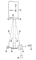
図1は、ウエハステージ10のZ軸に沿った位置情報を取得するための他の手法を描いたものである。この手法は、Loopstraによる従来例に詳細が説明されている(特許文献1を参照のこと)。図示されたウエハ12は、投影用オプティクスまたは露光ツール14による露光を実施するためにステージ上で支持されている。この手法における利点は、干渉計16がステージ10の側部に配置されてはいるものの、正確なZ軸計測値を得ることができるという点である。これは、露光システムのZ軸に対して平行なZ計測軸18を確立するミラーを適正に配置することにより可能となっている。第一のミラー22はステージ10のX方向またはY方向に沿った移動に対して45度の角度となるように配置されている。干渉計からの計測ビーム24は、この45度ミラーへと突き当たり、Z計測軸18を確立する。露光システムの構造体28には水平ミラー26が取り付けられており、これによりビームの向きが第一のミラー22へと向かうように変えられ、第一のミラーが戻ってきたビームを反射して干渉計16へと向けるのである。計測ビーム24に加え、干渉計はステージ10の垂直面31からの反射用に試験ビーム30も投射する。
FIG. 1 depicts another method for obtaining position information along the Z-axis of the
図1から明らかなように、ウエハステージ10のZ軸20に沿った動きは、45度ミラー22から水平ミラー26までのビーム経路セグメントの長さを変える結果となる。そのため、干渉計16がステージの側部にある間は、計測ビーム24は、ステージのZ軸転位と連動して長さを変える経路セグメントを持つ。実際には、水平ミラー26からの45度ミラーへの反射は、ステージのZ軸移動と連動して変化する第二のビーム経路セグメントを作る。一方、試験ビーム30の各ビーム経路セグメントの長さは、ステージ10がX方向に移動しない限り固定である。
As is apparent from FIG. 1, the movement of the
図1を参照して説明した手法は、その意図した目的においてはうまく作用するが、水平ミラー26が高度の平面性を要求する相対的に大型の部品であることから、コスト的な問題が生じている。さらに、集積回路の機構の線幅が小さくなるに従って、投影オプティクス14の投影レンズのサイズは大きくなる。これにより、図1においては投影オプティクスの直径が大きくなることになる。この結果、ステージの移動範囲全体をカバーする水平ミラー26の条件により、線幅の更なる微細化を行うことが潜在的に困難であるという問題が起きている。
While the approach described with reference to FIG. 1 works well for its intended purpose, the
投影レンズのサイズ増大が問題にならないシステムについても、図1と同様の種類および配向の水平ミラーの利用を避けたほうが良い他の理由が存在する場合がある。 There may be other reasons for avoiding the use of horizontal mirrors of the same type and orientation as in FIG. 1 for systems where the increase in size of the projection lens is not a problem.
すなわち、投影オプティクスの投影レンズの大型化に伴い、水平ミラーなどの部品により高度の平面性を要求されるか、水平ミラーなどの部品の利用を避けたほうがよい場合がありうる。 That is, with the increase in the size of the projection lens of the projection optics, there may be a case where a high degree of flatness is required by a component such as a horizontal mirror or it is better to avoid using a component such as a horizontal mirror.
この可動式装置が部品として含まれるシステム全体のパフォーマンスまたはデザインに影響を与える位置に、干渉計またはそのビーム・ステアリング部材のいずれかを配置させなければならないという必要性を生じさせることなく、可動式装置の特定軸に対する位置情報を取得するためのシステムを実現することができる。例えば、この可動式装置がウエハステージであり、特定軸が垂直のZ軸である場合には、システムの位置情報取得用ビーム・ステアリング部材は、ウエハステージの真上または直下には置かれない。 Mobile equipment without the need to place either an interferometer or its beam steering member in a position that affects the performance or design of the overall system in which the mobile equipment is included as a part A system for acquiring position information with respect to a specific axis of the apparatus can be realized. For example, when the movable apparatus is a wafer stage and the specific axis is a vertical Z axis, the beam steering member for acquiring position information of the system is not placed directly above or directly below the wafer stage.
本発明の一実施例においては、システムは第一および第二の反射面を持つ可動式装置と、ビームをこれらの反射面へと突き当たるように向ける位置に設けられた干渉計と、可動式装置の軸に沿った移動と連動して長さの変化するビーム経路セグメントを必要とすることなく反射されたビームを制御してビーム結合器へと届けるために、干渉計および反射面に対して配置されたビーム・ステアリング部材とを含む。可動式装置とは、集積回路の製作ステップ間で移動させるためにウエハまたはレチクルを載せた「ウエハステージ」とすることができる。このアプリケーションにおいては、「特定の軸」とはZ軸(例えばリソグラフィーの光学軸)とすることができ、また、反射面はZ軸に平行なウエハステージの側面にある。しかしながら、第一および第二の反射面は、Z軸自体に対して非平行である。 In one embodiment of the present invention, the system includes a movable device having first and second reflective surfaces, an interferometer provided in a position to direct the beam against these reflective surfaces, and the movable device. Positioned relative to the interferometer and reflecting surface to control and deliver the reflected beam to the beam combiner without the need for a beam path segment of varying length in conjunction with movement along the axis A beam steering member. A moveable device may be a “wafer stage” on which a wafer or reticle is mounted for movement between integrated circuit fabrication steps. In this application, the “specific axis” can be the Z axis (eg, the lithographic optical axis) and the reflective surface is on the side of the wafer stage parallel to the Z axis. However, the first and second reflecting surfaces are non-parallel to the Z axis itself.
ビーム結合器への到達時における第一のビームの第二のビームからの乖離を制御するためには、第一および第二の反射面の角度とビーム・ステアリング部材の配置および角度との選択は、可動式装置が位置情報が取得される軸に沿って移動された場合に2本のビーム経路長が逆に変化することになるように行われることが望ましい。可動式装置の特定軸に沿った移動に対してほぼ垂直の角度をなし、第一および第二のビームを制御するように干渉計を構成することができ、この場合には、第一および第二の反射面は、その垂直の角度に対して測定された場合に逆向きに傾斜している。ビーム・ステアリング部材は第一および第二のビームリターン・ミラーを含むことがあり、これらは第一および第二の反射面にアライメントされるようにそれぞれ配置されており、その配置は、ビームが干渉計へと戻る場合にそれらの元のビーム経路セグメントが(例えば、平面ミラーの場合などの)再度辿るようになっているか、または(例えば、ルーフミラーの場合などの)平行となるようになっている。 To control the divergence of the first beam from the second beam upon reaching the beam combiner, the selection of the angle of the first and second reflecting surfaces and the placement and angle of the beam steering member is It is desirable that the two beam path lengths change in the opposite direction when the movable device is moved along an axis from which position information is obtained. The interferometer can be configured to control the first and second beams at an angle that is substantially perpendicular to the movement of the mobile device along a particular axis, in which case the first and second The two reflective surfaces are inclined in the opposite direction when measured with respect to their vertical angle. The beam steering member may include first and second beam return mirrors that are arranged to be aligned with the first and second reflective surfaces, respectively, so that the beam interferes with it. When returning to the meter, their original beam path segments are retraced (eg, for a plane mirror) or parallel (eg, for a roof mirror) Yes.
位置情報を得るために干渉計システムを利用したこの方法によれば、第一および第二のビームが作られ、可動式装置へと向けられる。先にも述べたように、ビームは両方とも特定の軸に対して90度とすることができる。2本のビームは、可動式装置が特定軸に沿ってビーム対称位置にある場合には、可動式装置へと突き当たる反射、または、可動式装置により反射されるビーム経路セグメントの各々が他方のビームの対応するビーム経路セグメントと対称となるように反射を通じて制御される。しかしながら、可動式装置がそのビーム対称位置から転位すると、ビーム経路セグメントの少なくとも一部は長さを変えることになり、これによって干渉計方式による位置情報判定の基準(basis)が提供される。2本のビームは、(例えば、周波数および/または偏光などの)異なる光学特性を有しており、これにより標準型干渉計技術を採用することができる。 According to this method using an interferometer system to obtain position information, first and second beams are created and directed to a mobile device. As mentioned earlier, both beams can be 90 degrees with respect to a particular axis. The two beams are reflected when they strike the movable device along a particular axis, or when each of the beam path segments reflected by the movable device is the other beam. Is controlled through reflection to be symmetric with the corresponding beam path segment. However, when the mobile device is displaced from its beam symmetric position, at least a portion of the beam path segment will change length, thereby providing a basis for position information determination in an interferometric manner. The two beams have different optical properties (eg, frequency and / or polarization), which can employ standard interferometer technology.
本システムおよび方法は、ウエハステージのX方向およびY方向における移動の範囲の外にウエハステージ上にある全ての光学部材を維持することができるものであり、それは、ウエハステージがその可能移動範囲を超えてZ方向に移動することをも想定することができる。この結果、光学部材の位置は、設計上の問題や本発明を用いたシステム全体の他の側面に影響を与えにくいものとなっているのである。 The present system and method is capable of maintaining all optical members on the wafer stage outside the range of movement of the wafer stage in the X and Y directions, which allows the wafer stage to limit its possible range of movement. It can also be assumed that it moves beyond the Z direction. As a result, the position of the optical member is less likely to affect design issues and other aspects of the overall system using the present invention.
特定軸に対する位置情報を取得するためのシステムを、リソグラフィーの環境下で使用した場合について説明する。しかしながら、本発明は他のアプリケーションにも利用可能である。本システムは、移動範囲が直交する軸の一方または両方における移動範囲と比べて比較的小さい応用例に好適である。図2では、リソグラフィーシステム34の露光軸32(すなわち焦点軸)と一致する垂直のZ方向に沿った動きをモニタするために、本システムを使用することができる。この応用例では、可動式装置はウエハステージ36と、第一の反射面40および第二の反射面42をもつプリズムリフレクタ38とを含んでいる。先にも述べたように、「ウエハステージ」という語は、本願においてはリソグラフィーシステムのレチクルを支持するステージを含むが、この場合には、ステージは図2に示すようにこのシステムの下部にではなく、上部にあることになる。いうまでもないが、リソグラフィーシステムは、回転させることにより軸を垂直以外とすることができる。
A case where a system for acquiring position information with respect to a specific axis is used in a lithography environment will be described. However, the present invention can also be used for other applications. The system is suitable for applications where the travel range is relatively small compared to the travel range on one or both of the axes that are orthogonal. In FIG. 2, the system can be used to monitor movement along a vertical Z direction that coincides with the exposure axis 32 (ie, the focal axis) of the
位置情報取得システムは、第一のビーム44および第二のビーム46の光源を含んでいる。可能性の一つとして、光源は、レーザー48とビーム分割・再結合器50とを含みうる。以下により詳細を説明するが、再結合ビームは検出器52へと向けられる。レーザー48と分割・再結合器50と検出器52とは、干渉計部品である。第一および第二のビームは、異なる周波数および偏向を有することがあり、ここでの異なる偏向は、ビームの分割および再結合を促進し、異なる周波数はビーム経路長の計測を促進するものであり、これらにより移動の検出および/または定量が可能となる。
The position information acquisition system includes a light source of a
図3は、この干渉計を実現する上で使用可能な部品の詳細構成を単なる一例として示したものである。レーザー48は、標準的な二周波光レーザーでありうる。周波数の差を作るには複数の方法があり、それらはゼーマン分裂および音響光学変調を含みうるがこれらに限られない。周波数差と共に垂直偏向成分を含むビームを提供するために、ヘリウムネオンレーザーを使用することができる。
FIG. 3 shows a detailed configuration of components that can be used to realize the interferometer as an example.
レーザー48からのビームは、偏光感度の高いビームスプリッタ54へと入る。特定の周波数および偏光を持つ第一のビーム44はビームスプリッタ中を通り、異なる周波数および偏光を持つ第二のビーム46は内部反射されて干渉計のミラー56へと向けられる。
The beam from the
ビームスプリッタ54から出る際に、第一および第二のビーム44、46は、4分の1波長板58および60をそれぞれ通過する。各4分の1波長板は円偏光を提供する。
Upon exiting
図3の実施例における各ビーム44および46の角度は、Z軸に対して90°である。従って、プリズムリフレクタ38の第一および第二の反射面40および42の角度は、入射されるビーム経路に対して45°未満となるべきである。45°以上の角度とした場合には、従前の手法における問題や欠点をその反射は持つことになるであろう。
The angle of each
プリズムリフレクタ38の第一および第二の反射面40、42は、次のビーム経路セグメントの角度を決定する。2本のビームを再度反射させるために、一対のビーム・ステアリング部材64および66が配置されている。この反射はウエハステージへと戻すものであるため、これらの2つの光学部材をビームリターン・ミラーと呼ぶことができる。
The first and second reflecting
プリズムリフレクタ38からの第二の反射により、第一および第二のビーム44、46は干渉計へと戻される。各ビームはその元の経路を辿って干渉計へと戻るものであり、ここで、第二のビーム46は、干渉計ミラー56により再び反射される。2つの偏光の配向は2つの4分の1波長板58および60を通過することにより変化し、今度は第一のビーム44が反射され、第二のビーム46が反射することなくビームスプリッタ54を通じて伝わるようになる。これにより、下部のポートからスプリッタを出て検出器52へと至る併合ビーム68が作られる。検出器は、従来から干渉計に用いられているいずれのものを使用しても良い。例えば、検出器は、従来の増幅器70および位相検出器72へと接続されたフォトダイオードでありうる。当該技術分野ではよく知られているように、位相のシフトは、ステージの転位に関わる位置情報の取得に使用することができる。
Due to the second reflection from the
図2に戻るが、反射面40と接触を持つ第一のビーム44の4つのビーム経路セグメントが第二のビーム46の対応するビームセグメントと対称になっていることから、ウエハステージ36は、現在「対称配置」にあると考えることができる。すなわち、第一のビームおよび第二のビームの伝播を比較すると、干渉計50とプリズムリフレクタ38との間の経路長が等しく、プリズムリフレクタとビームステアリング・ミラー64および66との間の経路長が等しい。しかしながら、ウエハステージ36がZ軸に沿って上方向または下方向に移動すると、経路セグメントの長さが逆に変化する。ウエハステージが下方向に移動した場合には、第一のビーム44の4つの関連経路セグメントの長さは短くなるが、これは第一の反射面がそのように傾斜しているためである。一方で、第二の反射面42の逆方向の傾斜により、下方への移動においては4つのビーム経路セグメントが長くなるのである。ウエハステージ36が上方向に移動した場合には、第一のビームについては経路セグメントの長さは大きくなるが、第二のビームの経路セグメントは短くなる。容易に明らかなように、4つの経路セグメントは均一に変化するため、各ビーム経路の合計の長さの変化は4倍にされる。長さ変化が乗算される結果、併合ビーム68に実施される位相検出処理を利用してウエハステージ36の正確な移動量測定ができる。
Returning to FIG. 2, since the four beam path segments of the
図4を参照すると、これは本発明の別の実施例を描いたものである。本実施例においては、図2および図3の単一のプリズムリフレクタに代えて一対のリフレクタ74、76が使用される。しかしながら、ここでも逆方向に傾斜した2つの反射面40および42が設けられている。より大きな相違点は、ビームの方向制御を提供するために平面ミラーを用いる代わりに、一対のルーフミラー78、80を使用している点である。ルーフミラーは90°の角度で接合された2つのミラーから成るものでありうる。ルーフミラーは、対称的なビームセグメントを作るものであればどのような配向に置かれていても良い。一部の実施例においては、この対称性に関する条件は若干緩和される場合があるが、このような応用例では、(例えばZ軸などの)対象となる軸に沿った可動式装置(例えばウエハステージ36)の移動と連動して長さの変化するビーム経路セグメントが無いことがある。
Referring to FIG. 4, this depicts another embodiment of the present invention. In this embodiment, a pair of
図4の位置情報取得システムの処理は、図2に示した実施例とほぼ同一である。しかしながら、第一および第二のビーム44、46のビーム帰還経路は、元のビーム伝播経路から若干離間することになる。それにもかかわらず、2つの反射面40、42が逆方向に傾斜し、ルーフミラーが適正に配向されているため、ウエハステージ36が対称位置にある場合には、(ここでは、第一のビーム44は、反射面40に突き当たっているか、または反射面40から反射されている)4本のビーム経路セグメントは、第二のビーム46の対応するビーム経路セグメントと対称になる。また、ステージがZ軸に沿って移動した場合には、2本のビーム経路は逆に変化することになる。
The processing of the position information acquisition system in FIG. 4 is almost the same as that in the embodiment shown in FIG. However, the beam return paths of the first and
ビーム分割・再結合器50の内部構成(図示せず)は、入射する2本のビームを検出器52へと向けた一本のビーム68へと再結合するように設計されている。その結果、ウエハステージ36に関する位置情報を従来技術の利用により取得することができる。
The internal configuration (not shown) of the beam splitter /
図5は本発明の他の実施例を描いたものである。図4と同様に、他の実施例に関連して説明したものと同じ部品は同じ符号で示した。レーザー48は、ビーム分割・再結合器50への入力を提供する。ビーム分割作用により、周波数および偏光のいずれか、または両方が異なる第一および第二のビームが提供される。
FIG. 5 depicts another embodiment of the present invention. As in FIG. 4, the same parts as those described in connection with the other embodiments are indicated by the same reference numerals.
図2と図3と図4の実施例と同様に、2本のビームの各々は、反射面40、42に突き当たるか、または、反射面40、42により反射された4つの経路セグメントを含む経路を辿るものである。符号82は第一のビームにおけるこれらのビームセグメントのうちの2つを示しており、符号84は第二のビームの対応する2つのビームセグメントを示している。同様に、符号86は第一のビームにおける他の2つのビームセグメントを示しており(これらは反射面40と接触している)、符号88は第二のビームの対応する2つのビームセグメントを示している。ウエハステージがそのビーム対称位置にある場合には、ビームセグメント82および86の組み合わせは、ビームセグメント84および88の組み合わせと対称になっている。
Similar to the embodiment of FIGS. 2, 3 and 4, each of the two beams impinges on the
第一のビームは、ビーム分割・再結合器50を出てから符号82に示すビームセグメントに沿って反射面40へと向けられる。対照的に、第二のビームは、ビーム分割・再結合器の上部ポートを出てから、ペンタミラー92に至る前に平面ミラー90により反射されている。代わりに、ミラー90はルーフミラーとすることもできる。第二のビームは、ペンタミラーの作用により、反射面42への最初のビーム経路セグメントを作る。両ビームの第二および第三のビーム経路セグメントは、反射面と平面ミラー90との間の戻り反射により作られる。最後に、第四のビーム経路セグメントは、その同じビームの第一のセグメントと同軸である。この結果、2本のビームは再結合されて検出器52へと向けられる。
The first beam leaves the beam splitter /
次に図6を参照すると、本発明を一実施例に従って実現するための処理フローは、第一および第二のビームを生成するステップ94を含んでいる。これらの2本のビームは、周波数および偏光のいずれか、または両方により区別できるものである。これらのビームが異なる周波数と直交する偏光を持つ場合には、性能が最大化される可能性が高い。異なるレーザーを用いることにより2本のビームを生成するか、または上述したビーム分割技術を利用することができる。
Referring now to FIG. 6, the process flow for implementing the present invention according to one embodiment includes
ステップ96においては、2本のビームは、ウエハステージなどの可動式装置に突き当たるように向けられる。図2では両方のビーム44、46は干渉計により向きが制御されているが、図5では第二のビームは平面ミラー90およびペンタミラー92から反射された後にのみ可動式装置へと向けられる実施例が描かれている。
In
ステップ98においては、ビームの反射を使用して対称なビームセグメントを作る。一部のアプリケーションでは対称性に対する条件が若干緩和されるが、このようなアプリケーションでは対象となる特定軸に沿った可動式装置の移動に連動して長さが変化するビームセグメントが無くなる可能性がある。特定の軸に沿って可動式装置が移動されると、一方のビームのビーム経路セグメントが長くなる一方で、他方のビームの経路セグメントが短くなることから、この対称性に影響が出る。それにもかかわらず、個々のセグメントにおける長さの相違は比較的小さく、関連する経路セグメントは「ほぼ対称」のままである。
In
ステップ100においては、2本のビームを併合する。従来の技術を利用することができる。そして、ステップ102においては、可動式装置に関する位置情報を判定する。先にも述べたように、位置情報の取得には位相検出法を用いることができる。
In
図示した本発明の実施例では、平面ミラーとルーフミラーとペンタミラーとが使用されているが、他の反射性部品に代えることもできる。さらに、屈折部品や回折部品やホログラフィック部品などの他の種類のビームリターン「ミラー」を使用することもできる。 In the illustrated embodiment of the present invention, a plane mirror, a roof mirror, and a pentamirror are used, but other reflective parts can be used. In addition, other types of beam return “mirrors” such as refractive, diffractive and holographic components can be used.
本発明の利点の1つは、第一および第二の反射面が可動式装置の、特定軸に対して平行な側部に設けられているという点から直接的に得られている。一部の応用例においては、このことは顕著な結果を有する。例えば、製造プロセス中のウエハステージの移動において残されていた設計上の制約は、非測定関連要因によって生じる。反射面と協働する光学部材は、ウエハステージが露光軸に垂直な方向に移動したときでもウエハステージの範囲外にある。そのため、光学部材が他の考慮事項に衝突することはない。 One of the advantages of the present invention is directly obtained in that the first and second reflecting surfaces are provided on the side of the movable device that is parallel to the specific axis. In some applications this has significant consequences. For example, design constraints left in the movement of the wafer stage during the manufacturing process are caused by non-measurement related factors. The optical member that cooperates with the reflecting surface is outside the range of the wafer stage even when the wafer stage moves in a direction perpendicular to the exposure axis. Therefore, the optical member does not collide with other considerations.
リソグラフィーや他の可能な光学応用例では、冷却目的や、粒子の付着による汚染リスクを低減するためにエアシャワーが設けられる。エアシャワーに離開(disruption)があると空気の屈折率の変動を生じる場合がありので、エアシャワーの均一性は重要である。このような屈折率の変動は、レーザー干渉計により計測される光位相の変動に繋がり、干渉計測定値エラーを発生させる可能性がある。所望の位置情報を所得する上で、従来技術と比較した場合の本発明の他の利点として、エアシャワーの均一性が増大する可能性が高いということが挙げられる。 In lithography and other possible optical applications, air showers are provided for cooling purposes and to reduce the risk of contamination due to particle adhesion. Air shower uniformity may be important because air showers may cause fluctuations in the refractive index of the air. Such a change in refractive index leads to a change in the optical phase measured by the laser interferometer, and may cause an interferometer measurement value error. Another advantage of the present invention compared to the prior art in obtaining desired location information is that the air shower uniformity is likely to increase.
ウエハステージの移動を判定するための従来手法の1つに、入射するレーザービームに対して45°の角度に置かれたステージミラー(図1)がある。1つの問題は、ステージが回転するに従い、ビーム/ミラー接点のs方向およびp方向へのビーム偏光アライメントが劣化し、偏光回転してしまうという点である。対照的に、図2と図3と図4と図5の実施例では、入射に対してほぼ直角のステージ反射面を使用しており、これにより偏光回転効果を最小化することができる。 One conventional technique for determining the movement of the wafer stage is a stage mirror (FIG. 1) placed at an angle of 45 ° with respect to the incident laser beam. One problem is that as the stage rotates, the beam polarization alignment in the s and p directions of the beam / mirror contact deteriorates and the polarization rotates. In contrast, the embodiments of FIGS. 2, 3, 4 and 5 use a stage reflecting surface that is substantially perpendicular to the incidence, thereby minimizing polarization rotation effects.
本発明の更なる利点として、ダイナミックレンジが改善されるという点がある。従来の手法においては、意図していない干渉計の2本のビームに対して異なるビームのねじれ(beam shear)が導入される。本発明では干渉するビーム間の相対的なビームのねじれを小さくすることによりダイナミックレンジを向上させている。さらに、相対的なビームのねじれの低減により、波面関連計測の効果が小さくなる。検出器における一方のビームからの他方のビームの乖離は、ウエハステージの移動等のアプリケーションにおいては十分に許容範囲内にある。 A further advantage of the present invention is that the dynamic range is improved. In conventional approaches, different beam shears are introduced for the two beams of the unintended interferometer. In the present invention, the dynamic range is improved by reducing the relative torsion of the interfering beams. Furthermore, the effect of wavefront related measurements is reduced due to the reduction of relative beam twist. The deviation of one beam from the other beam at the detector is well within an acceptable range in applications such as wafer stage movement.
32 特定軸
34 リソグラフィーシステム
36 可動式装置
40 第一の反射面
42 第二の反射面
44 第一のビーム
46 第二のビーム
50 ビーム結合器
52 検出器
64、66、78、80、90、92 ビーム・ステアリング部材
82、86 第一のビームのビーム経路セグメント
84、88 第二のビームのビーム経路セグメント
32
Claims (4)
第一のビームが前記第一の反射面へと当たり、第二のビームが前記第二の反射面へと当たるように向ける干渉計であって、検出器に対して位置合わせされ、前記第一および第二のビームを結合させて該ビーム間での位相シフト量を測定するように位置合わせされたビーム結合器を含むものである干渉計と、
前記第一および第二のビームが、前記ビーム結合器に至るように、前記第一および第二の反射面の間を通り、前記可動式装置の前記特定軸に対して垂直な面に対して対称となるように配置されたビーム・ステアリング部材と
を含んでなる、特定軸に関連する位置情報を取得するためのシステム。 A movable device having first and second reflective surfaces on sides associated with a line parallel to a particular axis, wherein the first and second reflective surfaces are not parallel to the particular axis A movable device that is inclined at an angle, and wherein the first and second reflecting surfaces are inclined in opposite directions;
An interferometer that directs a first beam to strike the first reflective surface and directs a second beam to the second reflective surface, the interferometer being aligned with respect to a detector, And an interferometer that includes a beam combiner aligned to combine the second beam and measure the amount of phase shift between the beams;
Said first and second beams, to reach the said beam combiner, it passes between the front Symbol first and second reflecting surfaces, with respect to a plane perpendicular to the specific axis of the movable device A system for obtaining position information relating to a specific axis, comprising:
第一および第二のビームを前記可動式装置に設けられた第一および第二の反射面にそれぞれ当てるように向けるステップであって、該第一および第二の反射面が前記特定軸に対して平行ではない同じ角度だけ傾いており、該第一および第二の反射面が互いに逆向きに傾いている、向けるステップと、
前記第一および第二のビームが、ビーム結合器に至るように、前記第一および第二の反射面の間を通り、前記可動式装置の前記特定軸に対して垂直な面に対して対称となるようにビーム・ステアリング部材を配置するステップと、
干渉法により前記位置情報を取得するための基準として、前記第一および第二のビームを前記ビーム結合器において結合させて該ビーム間での位相シフト量を測定するステップと
を含んでなる方法。 A method for obtaining position information along a particular axis of a mobile device using an interferometer system, comprising:
Directing the first and second beams to respectively strike first and second reflecting surfaces provided on the movable device, wherein the first and second reflecting surfaces are directed to the specific axis. Tilting by the same angle that is not parallel and the first and second reflecting surfaces are tilted in opposite directions;
Before SL first and second beams, to reach the beam combiner passes between said first and second reflecting surfaces, with respect to a plane perpendicular against the specific axis of the movable device Arranging the beam steering member to be symmetrical ;
Combining the first and second beams in the beam combiner as a reference for obtaining the position information by interferometry and measuring a phase shift amount between the beams.
Applications Claiming Priority (2)
| Application Number | Priority Date | Filing Date | Title |
|---|---|---|---|
| US10/783199 | 2004-02-20 | ||
| US10/783,199 US7130056B2 (en) | 2004-02-20 | 2004-02-20 | System and method of using a side-mounted interferometer to acquire position information |
Publications (3)
| Publication Number | Publication Date |
|---|---|
| JP2005233966A JP2005233966A (en) | 2005-09-02 |
| JP2005233966A5 JP2005233966A5 (en) | 2008-03-21 |
| JP4880232B2 true JP4880232B2 (en) | 2012-02-22 |
Family
ID=34861174
Family Applications (1)
| Application Number | Title | Priority Date | Filing Date |
|---|---|---|---|
| JP2005044034A Active JP4880232B2 (en) | 2004-02-20 | 2005-02-21 | System and method for obtaining location information |
Country Status (5)
| Country | Link |
|---|---|
| US (1) | US7130056B2 (en) |
| JP (1) | JP4880232B2 (en) |
| CN (1) | CN1306241C (en) |
| DE (1) | DE102004059400A1 (en) |
| NL (1) | NL1028349C2 (en) |
Families Citing this family (45)
| Publication number | Priority date | Publication date | Assignee | Title |
|---|---|---|---|---|
| US7101053B2 (en) * | 2004-01-15 | 2006-09-05 | Associated Universities, Inc. | Multidirectional retroreflectors |
| US7362447B2 (en) * | 2004-02-20 | 2008-04-22 | Agilent Technologies, Inc. | Low walk-off interferometer |
| US7158236B2 (en) * | 2004-05-21 | 2007-01-02 | Agilent Technologies, Inc. | Heterodyne laser interferometer for measuring wafer stage translation |
| US8693006B2 (en) * | 2005-06-28 | 2014-04-08 | Nikon Corporation | Reflector, optical element, interferometer system, stage device, exposure apparatus, and device fabricating method |
| US7355719B2 (en) * | 2005-08-16 | 2008-04-08 | Agilent Technologies, Inc. | Interferometer for measuring perpendicular translations |
| JPWO2007142351A1 (en) * | 2006-06-09 | 2009-10-29 | 株式会社ニコン | MOBILE DEVICE, EXPOSURE APPARATUS, EXPOSURE METHOD, AND DEVICE MANUFACTURING METHOD |
| JPWO2008136404A1 (en) * | 2007-04-27 | 2010-07-29 | 株式会社ニコン | Optical member, interferometer system, stage apparatus, exposure apparatus, and device manufacturing method |
| JP2010122183A (en) * | 2008-11-21 | 2010-06-03 | Sanyo Electric Co Ltd | Object detecting device and information acquiring device |
| CN102109769B (en) * | 2009-12-29 | 2012-10-03 | 上海微电子装备有限公司 | Joint adjusting device and joint adjusting method of workpiece stage interferometer and mask stage interferometer |
| DE102013224381A1 (en) * | 2012-12-20 | 2014-06-26 | Dr. Johannes Heidenhain Gmbh | Optical position measuring device |
| CN103528509B (en) * | 2013-10-11 | 2015-02-11 | 哈尔滨工业大学 | Angular displacement laser interferometer calibrating method and device based on dual-standard optical axis gas bath |
| CN103499278B (en) * | 2013-10-11 | 2015-03-11 | 哈尔滨工业大学 | Method and device for calibrating morphology compensation type four-optical-axis linear displacement laser interferometer |
| CN103499285B (en) * | 2013-10-11 | 2015-02-11 | 哈尔滨工业大学 | Method and device for calibrating optically biaxial compensation and gas bath type linear displacement laser interferometer |
| CN103499281B (en) * | 2013-10-11 | 2015-03-11 | 哈尔滨工业大学 | Method and device for calibrating four-optical-axis return and gas bath type linear displacement laser interferometer |
| CN103499292B (en) * | 2013-10-11 | 2015-03-11 | 哈尔滨工业大学 | Angular displacement laser interferometer calibration method and device based on two standard optical axes |
| CN103528508B (en) * | 2013-10-11 | 2015-03-11 | 哈尔滨工业大学 | Morphology compensation type double-optical-axis angular displacement laser interferometer calibration method and device |
| CN103499286B (en) * | 2013-10-11 | 2015-03-11 | 哈尔滨工业大学 | Reset compensation type two-optical-axis linear displacement laser interferometer calibration method and device |
| CN103499280B (en) * | 2013-10-11 | 2015-04-22 | 哈尔滨工业大学 | Reset compensation type three-optical-axis linear displacement laser interferometer calibration method and device |
| CN103499287B (en) * | 2013-10-11 | 2015-03-11 | 哈尔滨工业大学 | Linear displacement laser interferometer calibration method and device based on two-standard-optical-axis air bath |
| CN103528505B (en) * | 2013-10-11 | 2015-02-11 | 哈尔滨工业大学 | Four-optical axis compensation and air bath type linear displacement laser interferometer calibration method and device |
| CN103499277B (en) * | 2013-10-11 | 2015-02-11 | 哈尔滨工业大学 | Angular displacement laser interferometer calibration method and device based on four standard optical axes |
| CN103528526B (en) * | 2013-10-11 | 2015-03-11 | 哈尔滨工业大学 | Morphology compensation type three-optical-axis linear displacement laser interferometer calibration method and device |
| CN103528503B (en) * | 2013-10-11 | 2015-03-11 | 哈尔滨工业大学 | Double-optical axis compensation and air bath type angular displacement laser interferometer calibration method and device |
| CN103528525B (en) * | 2013-10-11 | 2015-02-11 | 哈尔滨工业大学 | Three-optical axis compensation and air bath type linear displacement laser interferometer calibration method and device |
| CN103499282B (en) * | 2013-10-11 | 2015-03-11 | 哈尔滨工业大学 | Calibration method and device for three-optical-axis return and air bath linear displacement laser interferometer |
| CN103528500B (en) * | 2013-10-11 | 2015-02-11 | 哈尔滨工业大学 | Linear displacement laser interferometer calibrating method and device based on four-standard optical axis |
| CN103528506B (en) * | 2013-10-11 | 2015-03-11 | 哈尔滨工业大学 | Four-optical axis returning and air bath type angular displacement laser interferometer calibration method and device |
| CN103499291B (en) * | 2013-10-11 | 2015-02-11 | 哈尔滨工业大学 | Calibration method and device of angular displacement laser interferometer based on four-standard-optical-axis gas bath |
| CN103528501B (en) * | 2013-10-11 | 2015-03-11 | 哈尔滨工业大学 | Linear displacement laser interferometer calibrating method and device based on four-standard light-axis gas bath |
| CN103499289B (en) * | 2013-10-11 | 2015-03-11 | 哈尔滨工业大学 | Method and device for calibrating morphology compensation type four-optical-axis angular displacement laser interferometer |
| CN103528504B (en) * | 2013-10-11 | 2015-03-11 | 哈尔滨工业大学 | Method and device for calibrating return compensation type four-optical-axis linear displacement laser interferometer |
| CN103499290B (en) * | 2013-10-11 | 2015-03-11 | 哈尔滨工业大学 | Method and device for calibrating optically biaxial return and gas bath type angular displacement laser interferometer |
| CN103528507B (en) * | 2013-10-11 | 2015-02-11 | 哈尔滨工业大学 | Method and device for calibrating return compensation type four-optical-axis angular displacement laser interferometer |
| CN103528510B (en) * | 2013-10-11 | 2015-02-11 | 哈尔滨工业大学 | Four-optical axis compensation and air bath type angular displacement laser interferometer calibration method and device |
| CN103528502B (en) * | 2013-10-11 | 2015-03-11 | 哈尔滨工业大学 | Method and device for calibrating return compensation type double-optical-axis angular displacement laser interferometer |
| CN103499288B (en) * | 2013-10-11 | 2015-03-11 | 哈尔滨工业大学 | Linear displacement laser interferometer calibration method and device based on three-standard-optical-axis air bath |
| CN103528499B (en) * | 2013-10-11 | 2015-03-11 | 哈尔滨工业大学 | Morphology compensation type double-optical-axis linear displacement laser interferometer calibration method and device |
| CN103499284B (en) * | 2013-10-11 | 2015-03-11 | 哈尔滨工业大学 | Method and device for calibrating optically biaxial return and gas bath type linear displacement laser interferometer |
| WO2016190921A1 (en) | 2015-02-05 | 2016-12-01 | Associated Universities, Inc. | Fiber optic based laser range finder |
| US10126411B2 (en) | 2015-03-13 | 2018-11-13 | Continental Advanced Lidar Solutions Us, Llc. | Beam steering LADAR sensor |
| CN106886143B (en) * | 2017-04-28 | 2019-08-09 | 电子科技大学 | Holoscan space length extracting method based on phase hologram correlation |
| IL273651B1 (en) * | 2017-10-04 | 2024-02-01 | Asml Netherlands Bv | Interferometric stage positioning apparatus |
| US10697893B2 (en) * | 2018-03-09 | 2020-06-30 | The Boeing Company | Specular variable angle absolute reflectance method and reflectometer |
| WO2020173652A1 (en) | 2019-02-28 | 2020-09-03 | Asml Netherlands B.V. | Stage system and lithographic apparatus |
| US11327013B2 (en) | 2020-05-15 | 2022-05-10 | The Boeing Company | Specular variable angle absolute reflectance method and reflectometer |
Family Cites Families (14)
| Publication number | Priority date | Publication date | Assignee | Title |
|---|---|---|---|---|
| US4891526A (en) | 1986-12-29 | 1990-01-02 | Hughes Aircraft Company | X-Y-θ-Z positioning stage |
| JPH0599612A (en) * | 1991-10-04 | 1993-04-23 | Nikon Corp | Laser interferometer |
| JP3164960B2 (en) | 1994-02-18 | 2001-05-14 | キヤノン株式会社 | Stage equipment |
| DE69722688T2 (en) * | 1996-02-29 | 2004-01-15 | Boeing Co | Fiber optic-coupled interferometric sensor |
| KR100525521B1 (en) * | 1996-10-21 | 2006-01-27 | 가부시키가이샤 니콘 | Exposure apparatus and exposure method |
| US6020964A (en) * | 1997-12-02 | 2000-02-01 | Asm Lithography B.V. | Interferometer system and lithograph apparatus including an interferometer system |
| US6208407B1 (en) | 1997-12-22 | 2001-03-27 | Asm Lithography B.V. | Method and apparatus for repetitively projecting a mask pattern on a substrate, using a time-saving height measurement |
| JP3413122B2 (en) * | 1998-05-21 | 2003-06-03 | キヤノン株式会社 | Positioning apparatus, exposure apparatus using the same, and device manufacturing method |
| TW490596B (en) | 1999-03-08 | 2002-06-11 | Asm Lithography Bv | Lithographic projection apparatus, method of manufacturing a device using the lithographic projection apparatus, device manufactured according to the method and method of calibrating the lithographic projection apparatus |
| US6603562B1 (en) * | 1999-10-29 | 2003-08-05 | Yokogawa Electric Corporation | Two-dimensional positioning apparatus and method for measuring laser light from the apparatus |
| EP1285222A4 (en) | 2000-05-17 | 2006-11-15 | Zygo Corp | Interferometric apparatus and method |
| JP2003015509A (en) * | 2001-06-27 | 2003-01-17 | Sony Corp | Device for exposing and recording image, and method for exposing and recording image |
| US7193726B2 (en) * | 2001-08-23 | 2007-03-20 | Zygo Corporation | Optical interferometry |
| CN2508215Y (en) * | 2001-11-09 | 2002-08-28 | 天津大学 | Polarization beam splitting shearing interferometer |
-
2004
- 2004-02-20 US US10/783,199 patent/US7130056B2/en not_active Expired - Fee Related
- 2004-12-09 DE DE102004059400A patent/DE102004059400A1/en not_active Withdrawn
- 2004-12-31 CN CNB2004100115232A patent/CN1306241C/en not_active Expired - Fee Related
-
2005
- 2005-02-18 NL NL1028349A patent/NL1028349C2/en not_active IP Right Cessation
- 2005-02-21 JP JP2005044034A patent/JP4880232B2/en active Active
Also Published As
| Publication number | Publication date |
|---|---|
| NL1028349C2 (en) | 2006-11-27 |
| CN1306241C (en) | 2007-03-21 |
| US20050185193A1 (en) | 2005-08-25 |
| DE102004059400A1 (en) | 2005-09-15 |
| JP2005233966A (en) | 2005-09-02 |
| US7130056B2 (en) | 2006-10-31 |
| CN1657865A (en) | 2005-08-24 |
| NL1028349A1 (en) | 2005-08-23 |
Similar Documents
| Publication | Publication Date | Title |
|---|---|---|
| JP4880232B2 (en) | System and method for obtaining location information | |
| JP2752003B2 (en) | Inspection interferometer with scanning function | |
| US6757066B2 (en) | Multiple degree of freedom interferometer | |
| EP2150770B1 (en) | Optical distance sensor | |
| US7450246B2 (en) | Measuring device and method for determining relative positions of a positioning stage configured to be moveable in at least one direction | |
| US6878916B2 (en) | Method for focus detection for optically detecting deviation of the image plane of a projection lens from the upper surface of a substrate, and an imaging system with a focus-detection system | |
| US6987569B2 (en) | Dynamic interferometer controlling direction of input beam | |
| JP3774476B2 (en) | Interferometer system using two wavelengths and lithographic apparatus comprising such a system | |
| US6819434B2 (en) | Multi-axis interferometer | |
| TWI568991B (en) | Encoder interferometry system, lithography system, and encoder interferometry method | |
| JP4150371B2 (en) | An improved lithographic interferometer apparatus. | |
| US9372068B2 (en) | Measuring apparatus including multi-wavelength interferometer | |
| US6912054B2 (en) | Interferometric stage system | |
| KR20060084852A (en) | Surface triangulation and profiling through a thin film coating | |
| US6509971B2 (en) | Interferometer system | |
| CN109313008B (en) | Optical system and method for sample measurement | |
| JP2003524152A (en) | Interferometer using polarization preserving optics | |
| JP2007052022A (en) | System for measuring object, and method for measuring vertical displacement | |
| JP4469604B2 (en) | Optical interferometry | |
| US9534934B2 (en) | High resolution encoder head | |
| CN111207844A (en) | Bilateral multi-plane inclined wave surface interferometer and detection method thereof | |
| US20050007601A1 (en) | Optical characterization of surfaces and plates | |
| US20240011762A1 (en) | Compact dual pass interferometer for a plane mirror interferometer | |
| Yashchuk et al. | Towards new generation long trace profiler LTP-2020: system design with different sensors in different operation modes | |
| JPH10281720A (en) | Stage device and wave front aberration measuring device using the same |
Legal Events
| Date | Code | Title | Description |
|---|---|---|---|
| A521 | Request for written amendment filed |
Free format text: JAPANESE INTERMEDIATE CODE: A523 Effective date: 20080130 |
|
| A621 | Written request for application examination |
Free format text: JAPANESE INTERMEDIATE CODE: A621 Effective date: 20080130 |
|
| A131 | Notification of reasons for refusal |
Free format text: JAPANESE INTERMEDIATE CODE: A131 Effective date: 20100730 |
|
| A521 | Request for written amendment filed |
Free format text: JAPANESE INTERMEDIATE CODE: A523 Effective date: 20101018 |
|
| A131 | Notification of reasons for refusal |
Free format text: JAPANESE INTERMEDIATE CODE: A131 Effective date: 20110311 |
|
| A521 | Request for written amendment filed |
Free format text: JAPANESE INTERMEDIATE CODE: A523 Effective date: 20110603 |
|
| TRDD | Decision of grant or rejection written | ||
| A01 | Written decision to grant a patent or to grant a registration (utility model) |
Free format text: JAPANESE INTERMEDIATE CODE: A01 Effective date: 20111104 |
|
| A01 | Written decision to grant a patent or to grant a registration (utility model) |
Free format text: JAPANESE INTERMEDIATE CODE: A01 |
|
| A61 | First payment of annual fees (during grant procedure) |
Free format text: JAPANESE INTERMEDIATE CODE: A61 Effective date: 20111201 |
|
| R150 | Certificate of patent or registration of utility model |
Ref document number: 4880232 Country of ref document: JP Free format text: JAPANESE INTERMEDIATE CODE: R150 Free format text: JAPANESE INTERMEDIATE CODE: R150 |
|
| FPAY | Renewal fee payment (event date is renewal date of database) |
Free format text: PAYMENT UNTIL: 20141209 Year of fee payment: 3 |
|
| S111 | Request for change of ownership or part of ownership |
Free format text: JAPANESE INTERMEDIATE CODE: R313113 |
|
| R350 | Written notification of registration of transfer |
Free format text: JAPANESE INTERMEDIATE CODE: R350 |
|
| R250 | Receipt of annual fees |
Free format text: JAPANESE INTERMEDIATE CODE: R250 |
|
| R250 | Receipt of annual fees |
Free format text: JAPANESE INTERMEDIATE CODE: R250 |
|
| R250 | Receipt of annual fees |
Free format text: JAPANESE INTERMEDIATE CODE: R250 |
|
| R250 | Receipt of annual fees |
Free format text: JAPANESE INTERMEDIATE CODE: R250 |
|
| R250 | Receipt of annual fees |
Free format text: JAPANESE INTERMEDIATE CODE: R250 |
|
| R250 | Receipt of annual fees |
Free format text: JAPANESE INTERMEDIATE CODE: R250 |
|
| R250 | Receipt of annual fees |
Free format text: JAPANESE INTERMEDIATE CODE: R250 |
|
| R250 | Receipt of annual fees |
Free format text: JAPANESE INTERMEDIATE CODE: R250 |
|
| R250 | Receipt of annual fees |
Free format text: JAPANESE INTERMEDIATE CODE: R250 |
|
| R250 | Receipt of annual fees |
Free format text: JAPANESE INTERMEDIATE CODE: R250 |