JP4877869B2 - Method for producing organic semiconductor element - Google Patents
Method for producing organic semiconductor element Download PDFInfo
- Publication number
- JP4877869B2 JP4877869B2 JP2004359575A JP2004359575A JP4877869B2 JP 4877869 B2 JP4877869 B2 JP 4877869B2 JP 2004359575 A JP2004359575 A JP 2004359575A JP 2004359575 A JP2004359575 A JP 2004359575A JP 4877869 B2 JP4877869 B2 JP 4877869B2
- Authority
- JP
- Japan
- Prior art keywords
- organic semiconductor
- semiconductor film
- baking
- electrode
- film
- Prior art date
- Legal status (The legal status is an assumption and is not a legal conclusion. Google has not performed a legal analysis and makes no representation as to the accuracy of the status listed.)
- Expired - Fee Related
Links
- 239000004065 semiconductor Substances 0.000 title claims description 176
- 238000004519 manufacturing process Methods 0.000 title claims description 26
- 238000000034 method Methods 0.000 claims description 52
- 238000010438 heat treatment Methods 0.000 claims description 18
- 238000001771 vacuum deposition Methods 0.000 claims description 5
- 239000011261 inert gas Substances 0.000 claims description 4
- 230000008018 melting Effects 0.000 claims description 4
- 238000002844 melting Methods 0.000 claims description 4
- 239000010408 film Substances 0.000 description 166
- 239000000758 substrate Substances 0.000 description 45
- 239000000463 material Substances 0.000 description 42
- 239000010410 layer Substances 0.000 description 33
- 239000004973 liquid crystal related substance Substances 0.000 description 32
- 238000007740 vapor deposition Methods 0.000 description 28
- 230000006866 deterioration Effects 0.000 description 20
- SLIUAWYAILUBJU-UHFFFAOYSA-N pentacene Chemical compound C1=CC=CC2=CC3=CC4=CC5=CC=CC=C5C=C4C=C3C=C21 SLIUAWYAILUBJU-UHFFFAOYSA-N 0.000 description 18
- -1 silver halide Chemical class 0.000 description 13
- 238000000151 deposition Methods 0.000 description 12
- VYPSYNLAJGMNEJ-UHFFFAOYSA-N Silicium dioxide Chemical compound O=[Si]=O VYPSYNLAJGMNEJ-UHFFFAOYSA-N 0.000 description 11
- 238000005259 measurement Methods 0.000 description 10
- 150000001875 compounds Chemical class 0.000 description 8
- PCCVSPMFGIFTHU-UHFFFAOYSA-N tetracyanoquinodimethane Chemical compound N#CC(C#N)=C1C=CC(=C(C#N)C#N)C=C1 PCCVSPMFGIFTHU-UHFFFAOYSA-N 0.000 description 8
- 229910052721 tungsten Inorganic materials 0.000 description 8
- QVGXLLKOCUKJST-UHFFFAOYSA-N atomic oxygen Chemical compound [O] QVGXLLKOCUKJST-UHFFFAOYSA-N 0.000 description 7
- 239000001301 oxygen Substances 0.000 description 7
- 229910052760 oxygen Inorganic materials 0.000 description 7
- WFKWXMTUELFFGS-UHFFFAOYSA-N tungsten Chemical compound [W] WFKWXMTUELFFGS-UHFFFAOYSA-N 0.000 description 7
- 239000010937 tungsten Substances 0.000 description 7
- IJGRMHOSHXDMSA-UHFFFAOYSA-N Atomic nitrogen Chemical compound N#N IJGRMHOSHXDMSA-UHFFFAOYSA-N 0.000 description 6
- 229910052581 Si3N4 Inorganic materials 0.000 description 6
- 229910052751 metal Inorganic materials 0.000 description 6
- 239000002184 metal Substances 0.000 description 6
- HQVNEWCFYHHQES-UHFFFAOYSA-N silicon nitride Chemical compound N12[Si]34N5[Si]62N3[Si]51N64 HQVNEWCFYHHQES-UHFFFAOYSA-N 0.000 description 6
- 238000004528 spin coating Methods 0.000 description 6
- 238000004544 sputter deposition Methods 0.000 description 6
- PXHVJJICTQNCMI-UHFFFAOYSA-N Nickel Chemical compound [Ni] PXHVJJICTQNCMI-UHFFFAOYSA-N 0.000 description 5
- 238000013459 approach Methods 0.000 description 5
- 230000008859 change Effects 0.000 description 5
- 239000010949 copper Substances 0.000 description 5
- 239000013078 crystal Substances 0.000 description 5
- 230000008021 deposition Effects 0.000 description 5
- 230000000694 effects Effects 0.000 description 5
- 235000012239 silicon dioxide Nutrition 0.000 description 5
- 229920003002 synthetic resin Polymers 0.000 description 5
- 239000000057 synthetic resin Substances 0.000 description 5
- 239000010409 thin film Substances 0.000 description 5
- XKRFYHLGVUSROY-UHFFFAOYSA-N Argon Chemical compound [Ar] XKRFYHLGVUSROY-UHFFFAOYSA-N 0.000 description 4
- 229910052782 aluminium Inorganic materials 0.000 description 4
- MWPLVEDNUUSJAV-UHFFFAOYSA-N anthracene Chemical compound C1=CC=CC2=CC3=CC=CC=C3C=C21 MWPLVEDNUUSJAV-UHFFFAOYSA-N 0.000 description 4
- 239000004020 conductor Substances 0.000 description 4
- 229920000547 conjugated polymer Polymers 0.000 description 4
- 229910052802 copper Inorganic materials 0.000 description 4
- 150000002678 macrocyclic compounds Chemical class 0.000 description 4
- 239000011368 organic material Substances 0.000 description 4
- 229920000620 organic polymer Polymers 0.000 description 4
- 229920003023 plastic Polymers 0.000 description 4
- 239000004033 plastic Substances 0.000 description 4
- 229920000139 polyethylene terephthalate Polymers 0.000 description 4
- 239000005020 polyethylene terephthalate Substances 0.000 description 4
- 125000006850 spacer group Chemical group 0.000 description 4
- FHCPAXDKURNIOZ-UHFFFAOYSA-N tetrathiafulvalene Chemical compound S1C=CSC1=C1SC=CS1 FHCPAXDKURNIOZ-UHFFFAOYSA-N 0.000 description 4
- 239000010936 titanium Substances 0.000 description 4
- OKTJSMMVPCPJKN-UHFFFAOYSA-N Carbon Chemical compound [C] OKTJSMMVPCPJKN-UHFFFAOYSA-N 0.000 description 3
- KDLHZDBZIXYQEI-UHFFFAOYSA-N Palladium Chemical compound [Pd] KDLHZDBZIXYQEI-UHFFFAOYSA-N 0.000 description 3
- BQCADISMDOOEFD-UHFFFAOYSA-N Silver Chemical compound [Ag] BQCADISMDOOEFD-UHFFFAOYSA-N 0.000 description 3
- NIXOWILDQLNWCW-UHFFFAOYSA-N acrylic acid group Chemical group C(C=C)(=O)O NIXOWILDQLNWCW-UHFFFAOYSA-N 0.000 description 3
- 239000000956 alloy Substances 0.000 description 3
- 239000002585 base Substances 0.000 description 3
- 230000015572 biosynthetic process Effects 0.000 description 3
- 230000007423 decrease Effects 0.000 description 3
- 238000010586 diagram Methods 0.000 description 3
- 238000001704 evaporation Methods 0.000 description 3
- 229910052757 nitrogen Inorganic materials 0.000 description 3
- BASFCYQUMIYNBI-UHFFFAOYSA-N platinum Chemical compound [Pt] BASFCYQUMIYNBI-UHFFFAOYSA-N 0.000 description 3
- 238000005498 polishing Methods 0.000 description 3
- 229920001709 polysilazane Polymers 0.000 description 3
- 239000010453 quartz Substances 0.000 description 3
- 229920005989 resin Polymers 0.000 description 3
- 239000011347 resin Substances 0.000 description 3
- 229910052814 silicon oxide Inorganic materials 0.000 description 3
- 229910052709 silver Inorganic materials 0.000 description 3
- 239000004332 silver Substances 0.000 description 3
- 229910052715 tantalum Inorganic materials 0.000 description 3
- 229910052719 titanium Inorganic materials 0.000 description 3
- XLYOFNOQVPJJNP-UHFFFAOYSA-N water Substances O XLYOFNOQVPJJNP-UHFFFAOYSA-N 0.000 description 3
- WCBPJVKVIMMEQC-UHFFFAOYSA-N 1,1-diphenyl-2-(2,4,6-trinitrophenyl)hydrazine Chemical group [O-][N+](=O)C1=CC([N+](=O)[O-])=CC([N+]([O-])=O)=C1NN(C=1C=CC=CC=1)C1=CC=CC=C1 WCBPJVKVIMMEQC-UHFFFAOYSA-N 0.000 description 2
- RYGMFSIKBFXOCR-UHFFFAOYSA-N Copper Chemical compound [Cu] RYGMFSIKBFXOCR-UHFFFAOYSA-N 0.000 description 2
- 229920012266 Poly(ether sulfone) PES Polymers 0.000 description 2
- 229920000265 Polyparaphenylene Polymers 0.000 description 2
- 229910004298 SiO 2 Inorganic materials 0.000 description 2
- XUIMIQQOPSSXEZ-UHFFFAOYSA-N Silicon Chemical compound [Si] XUIMIQQOPSSXEZ-UHFFFAOYSA-N 0.000 description 2
- XBDYBAVJXHJMNQ-UHFFFAOYSA-N Tetrahydroanthracene Natural products C1=CC=C2C=C(CCCC3)C3=CC2=C1 XBDYBAVJXHJMNQ-UHFFFAOYSA-N 0.000 description 2
- 229910052783 alkali metal Inorganic materials 0.000 description 2
- 150000001340 alkali metals Chemical class 0.000 description 2
- 229910052784 alkaline earth metal Inorganic materials 0.000 description 2
- 150000001342 alkaline earth metals Chemical class 0.000 description 2
- HSFWRNGVRCDJHI-UHFFFAOYSA-N alpha-acetylene Natural products C#C HSFWRNGVRCDJHI-UHFFFAOYSA-N 0.000 description 2
- XAGFODPZIPBFFR-UHFFFAOYSA-N aluminium Chemical compound [Al] XAGFODPZIPBFFR-UHFFFAOYSA-N 0.000 description 2
- 229910052786 argon Inorganic materials 0.000 description 2
- 238000007611 bar coating method Methods 0.000 description 2
- 230000004888 barrier function Effects 0.000 description 2
- 239000002041 carbon nanotube Substances 0.000 description 2
- 229910021393 carbon nanotube Inorganic materials 0.000 description 2
- 150000001746 carotenes Chemical class 0.000 description 2
- 235000005473 carotenes Nutrition 0.000 description 2
- 238000005266 casting Methods 0.000 description 2
- 230000001413 cellular effect Effects 0.000 description 2
- 238000004140 cleaning Methods 0.000 description 2
- 229910052681 coesite Inorganic materials 0.000 description 2
- 229910052906 cristobalite Inorganic materials 0.000 description 2
- 238000007598 dipping method Methods 0.000 description 2
- KPUWHANPEXNPJT-UHFFFAOYSA-N disiloxane Chemical class [SiH3]O[SiH3] KPUWHANPEXNPJT-UHFFFAOYSA-N 0.000 description 2
- 239000010931 gold Substances 0.000 description 2
- 230000006872 improvement Effects 0.000 description 2
- AMGQUBHHOARCQH-UHFFFAOYSA-N indium;oxotin Chemical compound [In].[Sn]=O AMGQUBHHOARCQH-UHFFFAOYSA-N 0.000 description 2
- 238000002347 injection Methods 0.000 description 2
- 239000007924 injection Substances 0.000 description 2
- 229910052750 molybdenum Inorganic materials 0.000 description 2
- KNMNNEPMKDJBDW-UHFFFAOYSA-N n-[2-(3,4-dimethoxyphenyl)ethyl]-1-(2,6-dimethylphenoxy)propan-2-amine;hydrochloride Chemical compound Cl.C1=C(OC)C(OC)=CC=C1CCNC(C)COC1=C(C)C=CC=C1C KNMNNEPMKDJBDW-UHFFFAOYSA-N 0.000 description 2
- MZYHMUONCNKCHE-UHFFFAOYSA-N naphthalene-1,2,3,4-tetracarboxylic acid Chemical class C1=CC=CC2=C(C(O)=O)C(C(=O)O)=C(C(O)=O)C(C(O)=O)=C21 MZYHMUONCNKCHE-UHFFFAOYSA-N 0.000 description 2
- YTVNOVQHSGMMOV-UHFFFAOYSA-N naphthalenetetracarboxylic dianhydride Chemical compound C1=CC(C(=O)OC2=O)=C3C2=CC=C2C(=O)OC(=O)C1=C32 YTVNOVQHSGMMOV-UHFFFAOYSA-N 0.000 description 2
- 229910052759 nickel Inorganic materials 0.000 description 2
- 230000003647 oxidation Effects 0.000 description 2
- 238000007254 oxidation reaction Methods 0.000 description 2
- 239000002245 particle Substances 0.000 description 2
- WSRHMJYUEZHUCM-UHFFFAOYSA-N perylene-1,2,3,4-tetracarboxylic acid Chemical class C=12C3=CC=CC2=CC=CC=1C1=C(C(O)=O)C(C(O)=O)=C(C(O)=O)C2=C1C3=CC=C2C(=O)O WSRHMJYUEZHUCM-UHFFFAOYSA-N 0.000 description 2
- CLYVDMAATCIVBF-UHFFFAOYSA-N pigment red 224 Chemical compound C=12C3=CC=C(C(OC4=O)=O)C2=C4C=CC=1C1=CC=C2C(=O)OC(=O)C4=CC=C3C1=C42 CLYVDMAATCIVBF-UHFFFAOYSA-N 0.000 description 2
- 238000009832 plasma treatment Methods 0.000 description 2
- 229920001197 polyacetylene Polymers 0.000 description 2
- 229920000767 polyaniline Polymers 0.000 description 2
- 239000011112 polyethylene naphthalate Substances 0.000 description 2
- 229920000128 polypyrrole Polymers 0.000 description 2
- 229920000123 polythiophene Polymers 0.000 description 2
- 229920002717 polyvinylpyridine Polymers 0.000 description 2
- 238000012545 processing Methods 0.000 description 2
- 102000004169 proteins and genes Human genes 0.000 description 2
- 108090000623 proteins and genes Proteins 0.000 description 2
- 230000009467 reduction Effects 0.000 description 2
- 238000011160 research Methods 0.000 description 2
- 238000007650 screen-printing Methods 0.000 description 2
- 229910052710 silicon Inorganic materials 0.000 description 2
- 239000010703 silicon Substances 0.000 description 2
- 239000000377 silicon dioxide Substances 0.000 description 2
- 239000002356 single layer Substances 0.000 description 2
- 239000000243 solution Substances 0.000 description 2
- 239000007858 starting material Substances 0.000 description 2
- 229910052682 stishovite Inorganic materials 0.000 description 2
- 125000001424 substituent group Chemical group 0.000 description 2
- IFLREYGFSNHWGE-UHFFFAOYSA-N tetracene Chemical compound C1=CC=CC2=CC3=CC4=CC=CC=C4C=C3C=C21 IFLREYGFSNHWGE-UHFFFAOYSA-N 0.000 description 2
- 238000012546 transfer Methods 0.000 description 2
- 229910052905 tridymite Inorganic materials 0.000 description 2
- ZCYVEMRRCGMTRW-UHFFFAOYSA-N 7553-56-2 Chemical compound [I] ZCYVEMRRCGMTRW-UHFFFAOYSA-N 0.000 description 1
- PXGOKWXKJXAPGV-UHFFFAOYSA-N Fluorine Chemical compound FF PXGOKWXKJXAPGV-UHFFFAOYSA-N 0.000 description 1
- 239000004642 Polyimide Substances 0.000 description 1
- 239000004372 Polyvinyl alcohol Substances 0.000 description 1
- 239000004809 Teflon Substances 0.000 description 1
- 229920006362 Teflon® Polymers 0.000 description 1
- ATJFFYVFTNAWJD-UHFFFAOYSA-N Tin Chemical compound [Sn] ATJFFYVFTNAWJD-UHFFFAOYSA-N 0.000 description 1
- GWEVSGVZZGPLCZ-UHFFFAOYSA-N Titan oxide Chemical compound O=[Ti]=O GWEVSGVZZGPLCZ-UHFFFAOYSA-N 0.000 description 1
- RTAQQCXQSZGOHL-UHFFFAOYSA-N Titanium Chemical compound [Ti] RTAQQCXQSZGOHL-UHFFFAOYSA-N 0.000 description 1
- NRTOMJZYCJJWKI-UHFFFAOYSA-N Titanium nitride Chemical compound [Ti]#N NRTOMJZYCJJWKI-UHFFFAOYSA-N 0.000 description 1
- 230000002411 adverse Effects 0.000 description 1
- 125000000217 alkyl group Chemical group 0.000 description 1
- 229910045601 alloy Inorganic materials 0.000 description 1
- 239000005407 aluminoborosilicate glass Substances 0.000 description 1
- 229910021417 amorphous silicon Inorganic materials 0.000 description 1
- 238000007743 anodising Methods 0.000 description 1
- 239000007864 aqueous solution Substances 0.000 description 1
- 150000004945 aromatic hydrocarbons Chemical class 0.000 description 1
- 229910052788 barium Inorganic materials 0.000 description 1
- DSAJWYNOEDNPEQ-UHFFFAOYSA-N barium atom Chemical compound [Ba] DSAJWYNOEDNPEQ-UHFFFAOYSA-N 0.000 description 1
- 229910052797 bismuth Inorganic materials 0.000 description 1
- JCXGWMGPZLAOME-UHFFFAOYSA-N bismuth atom Chemical compound [Bi] JCXGWMGPZLAOME-UHFFFAOYSA-N 0.000 description 1
- 239000005388 borosilicate glass Substances 0.000 description 1
- 229910052799 carbon Inorganic materials 0.000 description 1
- 230000015556 catabolic process Effects 0.000 description 1
- 238000005229 chemical vapour deposition Methods 0.000 description 1
- 229920001940 conductive polymer Polymers 0.000 description 1
- 229910021419 crystalline silicon Inorganic materials 0.000 description 1
- 238000000354 decomposition reaction Methods 0.000 description 1
- 230000003247 decreasing effect Effects 0.000 description 1
- 238000006731 degradation reaction Methods 0.000 description 1
- 238000011161 development Methods 0.000 description 1
- 238000009792 diffusion process Methods 0.000 description 1
- 238000001035 drying Methods 0.000 description 1
- 239000007772 electrode material Substances 0.000 description 1
- 230000008020 evaporation Effects 0.000 description 1
- 230000002349 favourable effect Effects 0.000 description 1
- 229910052731 fluorine Inorganic materials 0.000 description 1
- 239000011737 fluorine Substances 0.000 description 1
- 229910021485 fumed silica Inorganic materials 0.000 description 1
- 239000007789 gas Substances 0.000 description 1
- 239000011521 glass Substances 0.000 description 1
- PCHJSUWPFVWCPO-UHFFFAOYSA-N gold Chemical compound [Au] PCHJSUWPFVWCPO-UHFFFAOYSA-N 0.000 description 1
- 229910052737 gold Inorganic materials 0.000 description 1
- FFUAGWLWBBFQJT-UHFFFAOYSA-N hexamethyldisilazane Chemical compound C[Si](C)(C)N[Si](C)(C)C FFUAGWLWBBFQJT-UHFFFAOYSA-N 0.000 description 1
- 239000001257 hydrogen Substances 0.000 description 1
- 229910052739 hydrogen Inorganic materials 0.000 description 1
- 125000004435 hydrogen atom Chemical class [H]* 0.000 description 1
- 229910052738 indium Inorganic materials 0.000 description 1
- APFVFJFRJDLVQX-UHFFFAOYSA-N indium atom Chemical compound [In] APFVFJFRJDLVQX-UHFFFAOYSA-N 0.000 description 1
- 239000011147 inorganic material Substances 0.000 description 1
- 150000002496 iodine Chemical class 0.000 description 1
- 229910052740 iodine Inorganic materials 0.000 description 1
- 239000011630 iodine Substances 0.000 description 1
- 239000011344 liquid material Substances 0.000 description 1
- 150000002736 metal compounds Chemical class 0.000 description 1
- 239000000203 mixture Substances 0.000 description 1
- 239000002105 nanoparticle Substances 0.000 description 1
- 239000012044 organic layer Substances 0.000 description 1
- 229910052763 palladium Inorganic materials 0.000 description 1
- IEQIEDJGQAUEQZ-UHFFFAOYSA-N phthalocyanine Chemical compound N1C(N=C2C3=CC=CC=C3C(N=C3C4=CC=CC=C4C(=N4)N3)=N2)=C(C=CC=C2)C2=C1N=C1C2=CC=CC=C2C4=N1 IEQIEDJGQAUEQZ-UHFFFAOYSA-N 0.000 description 1
- 238000005268 plasma chemical vapour deposition Methods 0.000 description 1
- 229910052697 platinum Inorganic materials 0.000 description 1
- 229920001690 polydopamine Polymers 0.000 description 1
- 229920001721 polyimide Polymers 0.000 description 1
- 239000002861 polymer material Substances 0.000 description 1
- 229920002451 polyvinyl alcohol Polymers 0.000 description 1
- 238000007639 printing Methods 0.000 description 1
- 230000008569 process Effects 0.000 description 1
- 230000003252 repetitive effect Effects 0.000 description 1
- FDNAPBUWERUEDA-UHFFFAOYSA-N silicon tetrachloride Chemical compound Cl[Si](Cl)(Cl)Cl FDNAPBUWERUEDA-UHFFFAOYSA-N 0.000 description 1
- 239000002002 slurry Substances 0.000 description 1
- 239000002904 solvent Substances 0.000 description 1
- 239000010935 stainless steel Substances 0.000 description 1
- 229910001220 stainless steel Inorganic materials 0.000 description 1
- 239000000126 substance Substances 0.000 description 1
- 238000004381 surface treatment Methods 0.000 description 1
- GUVRBAGPIYLISA-UHFFFAOYSA-N tantalum atom Chemical compound [Ta] GUVRBAGPIYLISA-UHFFFAOYSA-N 0.000 description 1
- JBQYATWDVHIOAR-UHFFFAOYSA-N tellanylidenegermanium Chemical compound [Te]=[Ge] JBQYATWDVHIOAR-UHFFFAOYSA-N 0.000 description 1
- 238000002230 thermal chemical vapour deposition Methods 0.000 description 1
- OGIDPMRJRNCKJF-UHFFFAOYSA-N titanium oxide Inorganic materials [Ti]=O OGIDPMRJRNCKJF-UHFFFAOYSA-N 0.000 description 1
- 239000013585 weight reducing agent Substances 0.000 description 1
Images


Landscapes
- Thin Film Transistor (AREA)
Description
本発明は、有機半導体膜を有する有機半導体素子及びその作製方法に関する。 The present invention relates to an organic semiconductor element having an organic semiconductor film and a manufacturing method thereof.
近年、薄膜半導体を有する薄膜トランジスタ(以下TFTともいう)を備えた表示装置に関する研究が進められ実用化されている。このTFTを備えた表示装置は、多数の画素を構成することが可能となることから高精細な表示装置を実現できる。またCRTと比べ低電圧で動作可能なことから低消費電力なことが知られている。さらにCRTのように大きな表示管を用いずに画面を構成できることから省スペース化が図れ、パーソナルコンピュータやPDA、そしてTVの表示部として広く使用されている。 In recent years, research on display devices including thin film transistors (hereinafter also referred to as TFTs) having thin film semiconductors has been advanced and put into practical use. Since a display device provided with this TFT can constitute a large number of pixels, a high-definition display device can be realized. Further, it is known that the power consumption is low because it can be operated at a lower voltage than the CRT. Further, since a screen can be configured without using a large display tube like a CRT, it can save space and is widely used as a display unit for personal computers, PDAs, and TVs.
今後の表示装置としての要求には、さらなる薄型化、軽量化、フレキシブル化があげられる。しかしこれまでのTFTは、半導体層として非晶質珪素や結晶質珪素などの無機半導体材料を用いて作製されるものがほとんどであった。このため無機半導体材料を用いてTFTを形成する場合には、半導体膜の形成に350℃を超える処理温度が必要となりプラスチック等の樹脂基板等の採用が制限されていた。 Future demands for display devices include further reduction in thickness, weight, and flexibility. However, most TFTs so far have been manufactured using an inorganic semiconductor material such as amorphous silicon or crystalline silicon as a semiconductor layer. For this reason, when a TFT is formed using an inorganic semiconductor material, a processing temperature exceeding 350 ° C. is required for forming the semiconductor film, and the use of a resin substrate such as plastic has been limited.
近年、半導体層として有機半導体を用いた有機薄膜トランジスタ(以下有機TFTと記す)の研究が進められている。有機TFTは、有機材料を使用しているので柔軟性に富んでいる。また無機半導体を用いたデバイスと比べると、より低温で形成することができるため、基板にプラスチック等の樹脂材料を使用できる。その結果、軽くて柔軟性があるデバイスを得ることができる。 In recent years, research on an organic thin film transistor (hereinafter referred to as an organic TFT) using an organic semiconductor as a semiconductor layer has been advanced. Organic TFTs are rich in flexibility because they use organic materials. In addition, since it can be formed at a lower temperature than a device using an inorganic semiconductor, a resin material such as plastic can be used for the substrate. As a result, a light and flexible device can be obtained.
更に有機TFTは、印刷法、インクジェット法、蒸着法等によるプロセスの簡略化が期待できるだけでなく、安価な基板材料を用いる事ができるため、装置の製造価格を抑えることができ、コスト的に有利なことが見積もれる。 Furthermore, organic TFTs can be expected not only to simplify the process by printing, ink jet, vapor deposition, etc., but also can use inexpensive substrate materials, which can reduce the manufacturing cost of the device and is advantageous in terms of cost. It can be estimated.
また、現在作製されている有機TFTは表面洗浄のみを行なったSiO2/Si基板と、表面洗浄後にHMDSで表面処理を行なった基板上に同一条件でペンタセンを積層したTFT素子を作製している(非特許文献1参照。)。
非特許文献1によると、表面処理を行なわない有機TFTは、チャネル長やチャネル幅が長い素子でしか移動度やオンオフ比および閾値において良いTFT特性が得られていない。
According to
しかし有機TFTを用いたデバイスを作製する際に、デバイスの小型化にはチャネル長やチャネル幅の短い素子の開発が必要不可欠である。 However, when manufacturing a device using an organic TFT, development of an element having a short channel length or channel width is indispensable for miniaturization of the device.
そこで本発明は上記非特許文献1とは異なる方法により、特性が改善された有機TFTを提供することを課題とする。
Accordingly, an object of the present invention is to provide an organic TFT having improved characteristics by a method different from that of Non-Patent
また、有機半導体は大気中に放置すると水や大気の影響で有機半導体が劣化し、TFT特性の低下を引き起こすというデメリットがある。さらに、有機半導体膜と電極および絶縁膜との密着性が有機半導体素子の特性の低下に影響を与えている。 In addition, when the organic semiconductor is left in the air, there is a demerit that the organic semiconductor is deteriorated due to the influence of water or air and the TFT characteristics are lowered. Furthermore, the adhesion between the organic semiconductor film, the electrode, and the insulating film affects the deterioration of the characteristics of the organic semiconductor element.
本発明は上記課題を鑑み、チャネル長やチャネル幅の短い素子においてもTFT特性の低下を防ぐことができる有機半導体素子の作製方法を提供する。 In view of the above-described problems, the present invention provides a method for manufacturing an organic semiconductor element that can prevent degradation of TFT characteristics even in an element having a short channel length or channel width.
本発明は有機半導体膜の蒸着後に素子を加熱(以下ベークと記す)することを特徴とする。 The present invention is characterized in that the element is heated (hereinafter referred to as baking) after the organic semiconductor film is deposited.
具体的な本発明の有機半導体素子の作製方法は、有機半導体膜を形成した後、有機半導体膜を、大気圧下又は減圧下で加熱することを特徴とする。 A specific method for producing an organic semiconductor element of the present invention is characterized in that after an organic semiconductor film is formed, the organic semiconductor film is heated under atmospheric pressure or reduced pressure.
本発明の有機半導体素子の作製方法は、ゲート電極を形成し、ゲート電極上に有機半導体膜を形成した後、有機半導体膜を、大気圧下又は減圧下で加熱し、加熱された有機半導体膜上にソース電極及びドレイン電極を形成することを特徴とする。 In the method for producing an organic semiconductor element of the present invention, a gate electrode is formed, an organic semiconductor film is formed on the gate electrode, and then the organic semiconductor film is heated under atmospheric pressure or reduced pressure. A source electrode and a drain electrode are formed thereon.
本発明の有機半導体素子の作製方法は、ゲート電極を形成し、ゲート電極上にソース電極及びドレイン電極を形成し、ソース電極及びドレイン電極上に有機半導体膜を形成した後、有機半導体膜を、大気圧下又は減圧下で加熱することを特徴とする。 In the method for producing an organic semiconductor element of the present invention, a gate electrode is formed, a source electrode and a drain electrode are formed on the gate electrode, an organic semiconductor film is formed on the source electrode and the drain electrode, Heating is performed under atmospheric pressure or reduced pressure.
本発明の有機半導体素子の作製方法は、無機膜に接して有機半導体膜を形成した後、有機半導体膜を、大気圧下又は減圧下で加熱することを特徴とする。 The method for manufacturing an organic semiconductor element of the present invention is characterized in that after an organic semiconductor film is formed in contact with an inorganic film, the organic semiconductor film is heated under atmospheric pressure or reduced pressure.
本発明の有機半導体素子の作製方法は、ゲート絶縁膜に接して有機半導体膜を形成した後、有機半導体膜を、大気圧下又は減圧下で加熱することを特徴とする。 The method for manufacturing an organic semiconductor element of the present invention is characterized in that after an organic semiconductor film is formed in contact with a gate insulating film, the organic semiconductor film is heated under atmospheric pressure or reduced pressure.
本発明において、有機半導体膜への加熱は、有機半導体膜材料の融点未満で行うとよい。 In the present invention, the heating to the organic semiconductor film is preferably performed below the melting point of the organic semiconductor film material.
本発明において、有機半導体膜への加熱は、250℃未満で行うとよい。 In the present invention, the organic semiconductor film is preferably heated at less than 250 ° C.
本発明において、有機半導体膜への加熱は有機半導体膜の粒界の大きさの平均値が10%以上成長しない温度で行うとよい。 In the present invention, the heating to the organic semiconductor film is preferably performed at a temperature at which the average value of the grain boundaries of the organic semiconductor film does not grow 10% or more.
以上のように形成される有機半導体素子は、作製工程における加熱温度が低いため、ポリエチレン−テレフタレート(PET)、ポリエチレンナフタレート(PEN)、ポリエーテルサルフォン(PES)に代表されるプラスチックや、アクリル等の合成樹脂からなる基板を用いることができる。 Since the organic semiconductor element formed as described above has a low heating temperature in the manufacturing process, plastics typified by polyethylene-terephthalate (PET), polyethylene naphthalate (PEN), and polyethersulfone (PES), and acrylic A substrate made of a synthetic resin such as can be used.
ベークは、大気圧下又は減圧下のどちらでもよいが、減圧下にすることによりベーク温度を低温化することができる。その結果、加熱による有機半導体素子の劣化を低減することが期待できる。特に、基板に合成樹脂を用いる場合、ベーク温度を低温とすると好ましい。またベークは、不活性ガス雰囲気で行ってもよい。 The baking may be performed under atmospheric pressure or reduced pressure, but the baking temperature can be lowered by reducing the pressure. As a result, it can be expected to reduce deterioration of the organic semiconductor element due to heating. In particular, when a synthetic resin is used for the substrate, it is preferable that the baking temperature is low. Baking may be performed in an inert gas atmosphere.
またゲート電極、又はソース電極及びドレイン電極は、スパッタリング法、インクジェット法、スピンコート法、及び蒸着法のいずれかを用いて、形成することができる。またゲート電極、ソース電極又はドレイン電極は、W、Ta、Ti、Mo、Al、Cuから選ばれた元素、又は元素を主成分とする合金材料もしくは化合物材料で形成することができる。 The gate electrode, the source electrode, and the drain electrode can be formed by any one of a sputtering method, an inkjet method, a spin coating method, and an evaporation method. The gate electrode, the source electrode, or the drain electrode can be formed using an element selected from W, Ta, Ti, Mo, Al, and Cu, or an alloy material or a compound material containing the element as a main component.
また本発明は、このように形成された有機半導体素子を得ることが出来、該有機半導体素子を液晶表示装置又は発光素子を有する表示装置の画素部に設け、半導体素子として使用することができる。特に合成樹脂上に有機半導体素子を設けることにより、液晶表示装置又は発光素子を有する表示装置のフレキシブル性を高め、軽量化を達成することができる。 In addition, according to the present invention, an organic semiconductor element formed as described above can be obtained, and the organic semiconductor element can be provided in a pixel portion of a display device having a liquid crystal display device or a light emitting element and used as a semiconductor element. In particular, by providing an organic semiconductor element over a synthetic resin, the flexibility of a liquid crystal display device or a display device having a light-emitting element can be improved and weight reduction can be achieved.
このような発明により、オンオフの閾値を変化させることができ、さらにオフ時のリーク電流を下げることができる。
これにより、オンオフの閾値を0Vに近づけることができ、オンオフ比を上げることができる。
このように有機半導体素子の特性を改善することができる。
According to such an invention, the on / off threshold value can be changed, and the leakage current at the off time can be further reduced.
Thereby, the on / off threshold value can be brought close to 0 V, and the on / off ratio can be increased.
Thus, the characteristics of the organic semiconductor element can be improved.
また、この改善により、短いチャネル長とチャネル幅の素子でも、実用可能なTFT特性を得ることが出来るようになり、表示装置等のデバイスの小型化が可能となる。 In addition, with this improvement, practical TFT characteristics can be obtained even with an element having a short channel length and channel width, and a device such as a display device can be downsized.
以下に、本発明の実施の形態を図面に基づいて説明する。
但し、本発 明は多くの異なる態様で実施することが可能であり、本発明の趣旨及びその範囲から 逸脱することなくその形態及び詳細を様々に変更し得ることは当業者であれば容易に 理解される。従って、本実施の形態の記載内容に限定して解釈されるものではない。
なお、実施の形態を説明するための全図において、同一部分又は同様な機能を有する部分には同一の符号を付し、その繰り返しの説明は省略する。
Embodiments of the present invention will be described below with reference to the drawings.
However, the present invention can be implemented in many different modes, and it is easy for those skilled in the art to make various changes in form and details without departing from the spirit and scope of the present invention. Understood. Therefore, the present invention is not construed as being limited to the description of this embodiment mode.
Note that in all the drawings for describing the embodiments, the same portions or portions having similar functions are denoted by the same reference numerals, and repetitive description thereof is omitted.
(実施の形態1)
本実施の形態では、ボトムコンタクト型の有機半導体素子として、有機TFTの作製方法について説明する。
(Embodiment 1)
In this embodiment mode, a method for manufacturing an organic TFT as a bottom contact type organic semiconductor element will be described.
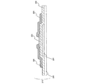
図1にボトムコンタクト型の有機TFTの断面図を示す。ボトムコンタクト型有機TFTとは、ソース電極及びドレイン電極を形成後、有機半導体膜を形成する素子構造を有する。 FIG. 1 shows a cross-sectional view of a bottom contact type organic TFT. The bottom contact type organic TFT has an element structure in which an organic semiconductor film is formed after forming a source electrode and a drain electrode.
まず、絶縁表面を有する基板100上にゲート電極として機能する導電膜(以下、ゲート電極と表記する)101を形成する。なお本実施の形態では絶縁表面を有する基板として、石英基板を用い、該石英基板上に導電膜としてタングステン(W)を用い、スパッタリング法にてゲート電極を形成する例で説明するが、本発明はこれに限定されない。
First, a conductive film 101 (hereinafter referred to as a gate electrode) 101 that functions as a gate electrode is formed over a
絶縁表面を有する基板には、例えばバリウムホウケイ酸ガラスや、アルミノホウケイ酸ガラスなどのガラス基板、ステンレス基板等を用いることができる。また好ましくは、ポリエチレン−テレフタレート(PET)、ポリエチレンナフタレート(PEN)、ポリエーテルサルフォン(PES)に代表されるプラスチックや、アクリル等の合成樹脂からなる基板を用いるとよい。このような合成樹脂から成る基板は、可撓性を有し、さらに軽量である。 As the substrate having an insulating surface, for example, a glass substrate such as barium borosilicate glass or alumino borosilicate glass, a stainless steel substrate, or the like can be used. Preferably, a substrate made of a plastic represented by polyethylene-terephthalate (PET), polyethylene naphthalate (PEN), or polyethersulfone (PES) or a synthetic resin such as acrylic is used. A substrate made of such a synthetic resin has flexibility and is lightweight.
また基板の平坦性を高めるため、化学的又は機械的ポリッシング法、いわゆるCMP法(Chemical−Mechanical Polishing)により、表面研磨してから用いると好ましい。CMPの研磨剤(スラリー)には、例えば、塩化シリコンガスを熱分解して得られるフュームドシリカ粒子をKOH水溶液に分散したものを用いることができる。 In order to improve the flatness of the substrate, it is preferable to use after polishing the surface by a chemical or mechanical polishing method, so-called CMP method (Chemical-Mechanical Polishing). As the CMP abrasive (slurry), for example, fumed silica particles obtained by thermally decomposing silicon chloride gas in a KOH aqueous solution can be used.
基板上には、必要に応じて下地膜を形成してもよい。下地膜は、基板中に含まれるNaなどのアルカリ金属やアルカリ土類金属が、半導体膜中に拡散し、半導体素子の特性に悪影響を及ぼすのを防ぐ機能を有する。そのため、アルカリ金属やアルカリ土類金属の半導体膜への拡散を抑えることができる酸化珪素、窒化珪素、窒化酸化珪素、酸化チタン、窒化チタンなどの絶縁膜を用いて下地膜を形成することができる。 A base film may be formed on the substrate as necessary. The base film has a function of preventing alkali metal such as Na or alkaline earth metal contained in the substrate from diffusing into the semiconductor film and adversely affecting the characteristics of the semiconductor element. Therefore, the base film can be formed using an insulating film such as silicon oxide, silicon nitride, silicon nitride oxide, titanium oxide, or titanium nitride that can suppress diffusion of alkali metal or alkaline earth metal into the semiconductor film. .
またゲート電極はタングステン以外に、Ta、Ti、Mo、Al、Cuから選ばれた元素、又は前記元素を主成分とする合金材料もしくは化合物材料で形成すればよい。さらにゲート電極は、単層構造又は積層構造を有することができる。またゲート電極はスパッタリング法の他、スクリーン印刷法、ロールコーター法又は液滴吐出法、スピンコート法、蒸着法などで形成しても良いし、電極材料は金属及び金属化合物の他、導電性高分子などを使用しても良い。 In addition to tungsten, the gate electrode may be formed of an element selected from Ta, Ti, Mo, Al, and Cu, or an alloy material or compound material containing the element as a main component. Further, the gate electrode can have a single layer structure or a stacked structure. In addition to the sputtering method, the gate electrode may be formed by a screen printing method, a roll coater method, a droplet discharge method, a spin coating method, a vapor deposition method, or the like. A molecule or the like may be used.
液滴吐出法は、選択的にパターンを形成可能な方法であり、導電膜や絶縁膜などの材料が混入された組成物の液滴(ドットとも表記する)を選択的に吐出(噴出)して導電膜を形成する方法である。液滴吐出法は、その方式によっては、インクジェット法とも呼ばれる。 The droplet discharge method is a method capable of selectively forming a pattern, and selectively discharges (spouts) a droplet (also referred to as a dot) of a composition mixed with a material such as a conductive film or an insulating film. This is a method for forming a conductive film. The droplet discharge method is also called an ink jet method depending on the method.
液滴吐出法により導電膜を形成する場合、溶媒に混在される導電体として、金(Au)、銀(Ag)、銅(Cu)、白金(Pt)、パラジウム(Pd)、タングステン(W)、ニッケル(Ni)、タンタル(Ta)、ビスマス(Bi)、鉛(Pb)、インジウム(In)、錫(Sn)、亜鉛(Zn)、チタン(Ti)、若しくはアルミニウム(Al)、これらからなる合金、これらの分散性ナノ粒子、又はハロゲン化銀の微粒子を用いることができる。 When a conductive film is formed by a droplet discharge method, gold (Au), silver (Ag), copper (Cu), platinum (Pt), palladium (Pd), tungsten (W) are used as conductors mixed in a solvent. , Nickel (Ni), tantalum (Ta), bismuth (Bi), lead (Pb), indium (In), tin (Sn), zinc (Zn), titanium (Ti), or aluminum (Al). Alloys, these dispersible nanoparticles, or silver halide particles can be used.
またスクリーン印刷法等により導電膜を形成する場合、導電性ペーストを用いる。導電性ペーストとしては、導電性カーボンペースト、導電性銀ペースト、導電性銅ペースト、導電性ニッケルなどを用いることができる。導電性ペーストで所定のパターンに形成した後は、レベリング、乾燥後、100〜200℃で硬化させるとよい。 In the case where a conductive film is formed by a screen printing method or the like, a conductive paste is used. As the conductive paste, conductive carbon paste, conductive silver paste, conductive copper paste, conductive nickel, or the like can be used. After the conductive paste is formed into a predetermined pattern, it may be cured at 100 to 200 ° C. after leveling and drying.
ゲート電極101を形成した後にゲート絶縁膜として機能する絶縁膜(以下、ゲート絶縁膜と表記する)102を形成する。なお本実施の形態のTFTは、ゲート絶縁膜102はSiONをCVD法にて成膜した例で説明するが、ゲート絶縁膜102はCVD法の他、スパッタ法、スピンコート法、蒸着法などで成膜しても良い。
After the
ゲート絶縁膜の材料は、窒化酸化ケイ素(SiON)、酸化ケイ素(SiO2)、窒化ケイ素(SiN)、ポリビニルアルコール、シロキサン、ポリシラザン等の無機物又は有機物を使用しても良い。シロキサンとは、珪素(Si)と酸素(O)との結合で骨格構造が構成され、置換基に少なくとも水素を含む、又は置換基にフッ素、アルキル基、又は芳香族炭化水素のうち少なくとも1種を有するポリマー材料、を出発原料として形成される。またポリシラザンとは、珪素(Si)と窒素(N)の結合を有するポリマー材料、いわゆるポリシラザンを含む液体材料を出発原料として形成される。 As the material of the gate insulating film, an inorganic or organic material such as silicon nitride oxide (SiON), silicon oxide (SiO 2 ), silicon nitride (SiN), polyvinyl alcohol, siloxane, or polysilazane may be used. Siloxane has a skeletal structure composed of a bond of silicon (Si) and oxygen (O), and the substituent contains at least hydrogen, or the substituent has at least one of fluorine, an alkyl group, and an aromatic hydrocarbon. A polymeric material having a starting material. Polysilazane is formed using a polymer material having a bond of silicon (Si) and nitrogen (N), that is, a liquid material containing so-called polysilazane as a starting material.
またゲート絶縁膜として用いる絶縁膜には、ゲート電極を陽極酸化して得られる絶縁膜を用いてもよい。 As the insulating film used as the gate insulating film, an insulating film obtained by anodizing the gate electrode may be used.
次にゲート絶縁膜102の上にTFTのソース電極またはドレイン電極として機能する導電膜(以下、ソース電極またはドレイン電極と表記する)103を形成する。なお本実施の形態のTFTは、ソース電極またはドレイン電極103としてタングステンをスパッタ法にて形成した例で説明するが、電極はスパッタ法の他、インクジェット法、スピンコート法、蒸着法などで形成しても良いし、電極材料は金属及び金属化合物の他、導電性高分子などを使用しても良い。すなわち、ゲート電極の材料又は作製方法を参照して、ソース電極またはドレイン電極103を形成することができる。
Next, a conductive film 103 (hereinafter referred to as a source electrode or a drain electrode) 103 that functions as a source electrode or a drain electrode of the TFT is formed over the
しかしながらソース電極またはドレイン電極は、有機半導体膜とオーミック接合する必要があるので、p型の有機半導体材料のときは、有機半導体材料のイオン化ポテンシャルよりも大きい仕事関数を持った材料を用いることが望ましく、n型の有機半導体材料のときは、有機半導体材料のイオン化ポテンシャルよりも小さい仕事関数を持った材料を用いることが望ましい。本実施の形態においては有機半導体材料としてp型のペンタセンを用いているので、仕事関数が比較的高いタングステンを用いる。 However, since the source electrode or the drain electrode needs to be in ohmic contact with the organic semiconductor film, it is desirable to use a material having a work function larger than the ionization potential of the organic semiconductor material in the case of a p-type organic semiconductor material. In the case of an n-type organic semiconductor material, it is desirable to use a material having a work function smaller than the ionization potential of the organic semiconductor material. In this embodiment mode, p-type pentacene is used as the organic semiconductor material, so that tungsten having a relatively high work function is used.
そして、絶縁膜102とソース電極またはドレイン電極103上に有機半導体膜104を成膜する。なお、本実施の形態の有機半導体材料としてはペンタセンを用いる例で説明するが、有機半導体膜材料としては、有機分子性結晶、有機高分子化合物を用いればよい。具体的な有機分子性結晶は、多環芳香族化合物、共役二重結合系化合物、カロテン、マクロ環化合物又はその錯体、フタロシアニン、電荷移動型錯体(CT錯体)等が挙げられる。例えば、アントラセン、テトラセン、ペンタセン、6T(ヘキサチオフェン)、TCNQ(テトラシアノキノジメタン)、TTF(テトラチアフルバレン):TCNQ(テトラシアノキノジメタン)錯体、DDPH(ジフェニルピクリルヒドラジル)、色素、タンパク、PTCDAなどのペリレンテトラカルボン酸誘導体、NTCDAなどのナフタレンテトラカルボン酸誘導体などを用いることができる。また、具体的な有機高分子化合物は、π共役系高分子、カーボンナノチューブ、ポリビニルピリジン、フロタシアニン金属錯体、ヨウ素錯体等が挙げられる。特に骨格が共役二重結合から構成されるπ共役系高分子である、ポリアセチレン、ポリアニリン、ポリピロール、ポリチエニレン、ポリチオフェン誘導体、ポリ(3アルキルチオフェン)、ポリパラフェニレン誘導体又はポリパラフェニレンビニレン誘導体を用いると好ましい。
Then, an
また成膜方法としては、膜厚の均一な膜が形成できる方法を用いればよい。具体的な方法としては、蒸着法、スピンコート法、バーコート法、溶液キャスト法、ディッピング法を用いればよい。 As a film formation method, a method capable of forming a film having a uniform thickness may be used. As a specific method, a vapor deposition method, a spin coating method, a bar coating method, a solution casting method, or a dipping method may be used.
また有機半導体膜形成前処理として、被形成面に対してプラズマ処理を行ったり、密着性又は界面状態を向上させるための膜、例えば自己組織化単分子膜(SAM)や配向膜を形成してもよい。 In addition, as a pretreatment for forming an organic semiconductor film, a plasma treatment is performed on a surface to be formed, or a film for improving adhesion or an interface state, for example, a self-assembled monomolecular film (SAM) or an alignment film is formed. Also good.
なお本実施の形態では、有機材料であるペンタセンを真空蒸着法によって飛ばすことにより、ゲート絶縁膜102と、ソース電極またはドレイン電極103上に有機半導体膜104を形成する。
Note that in this embodiment, the
そして、有機半導体膜の形成後に素子基板110をベークする。このときの温度は、有機半導体膜104が蒸発又は分解するよりも低い温度を上限とする。この温度範囲であって、高温の方が有機TFT特性の改善に効果的である。また、このときの温度は、有機半導体膜の融点以下が望ましい。ベークすることによりTFT特性が改善する要因の1つとして、ベークにより有機半導体膜104とソース電極またはドレイン電極103および絶縁膜102との密着性が向上し、注入障壁が小さくなるためキャリア輸送性が向上するためと推測される。また、高温のほうが、より有機半導体膜104とソース電極またはドレイン電極103及び絶縁膜102との密着性が向上し、TFT特性の改善に効果的であると推測される。さらに、ベークの効果で、有機半導体膜104中に含まれる水分が減少するため有機半導体膜104の劣化が抑えられ、ベーク前に比べてTFT特性が改善すると予想される。
Then, the
実施例6で示す、有機半導体材料としてペンタセンを用いたベーク前後の結果を見ると、ベーク時の温度はベーク前後のペンタセンの粒界(結晶粒)が成長しない温度が好ましい。 Looking at the results before and after baking using pentacene as the organic semiconductor material shown in Example 6, the temperature during baking is preferably such that the grain boundaries (crystal grains) of pentacene before and after baking do not grow.
実施例1で示す、有機半導体材料としてペンタセンを用いた大気下ベークの結果をみると、120℃、150℃、200℃と温度が高くなるにつれて、閾値のシフトが小さくなっている。すなわち、高温の方が有機TFT特性の改善に効果的であることが分かる。また実施例1により、有機半導体材料としてペンタセンを用いた場合、250℃が蒸発又は分解する温度付近であることがわかり、加熱温度は250℃未満がよい。ベークにより有機半導体材料とソース電極またはドレイン電極及び絶縁膜との密着性が向上し、注入障壁が小さくなるためキャリア輸送性が向上し、TFT特性が改善していると推測される。高温のほうが、より有機半導体膜とソース電極またはドレイン電極および絶縁膜との密着性が向上し、TFT特性の改善にさらに効果的であると推測される。また、ベークにより有機半導体膜中に含まれる水分が減少するため有機半導体膜の劣化が抑えられ、ベーク前に比べてTFT特性が向上していると推測される。 Looking at the results of baking in air using pentacene as the organic semiconductor material shown in Example 1, the threshold shift decreases as the temperature increases to 120 ° C., 150 ° C., and 200 ° C. That is, it can be seen that the higher temperature is more effective in improving the organic TFT characteristics. Further, according to Example 1, when pentacene is used as the organic semiconductor material, it can be seen that 250 ° C. is around the temperature at which evaporation or decomposition occurs, and the heating temperature is preferably less than 250 ° C. It is presumed that the baking improves the adhesion between the organic semiconductor material, the source or drain electrode, and the insulating film, reduces the injection barrier, improves the carrier transportability, and improves the TFT characteristics. It is presumed that the higher temperature improves the adhesion between the organic semiconductor film and the source or drain electrode and the insulating film, and is more effective in improving the TFT characteristics. In addition, since the moisture contained in the organic semiconductor film is reduced by baking, the deterioration of the organic semiconductor film is suppressed, and it is estimated that the TFT characteristics are improved as compared with those before baking.
またベーク中の雰囲気は、大気中で行なっても効果があるが、酸素や水による有機半導体膜の劣化を考慮して窒素やアルゴンなどの不活性ガス雰囲気で行なっても良い。さらに、有機半導体膜の劣化を抑えることとベーク温度の低温化を狙って減圧中(例えば1.3×10⁻³Pa〜6.7×10⁴Pa)でベークを行なっても良い。 The atmosphere during baking is effective even when performed in the air, but may be performed in an inert gas atmosphere such as nitrogen or argon in consideration of deterioration of the organic semiconductor film due to oxygen or water. Further, baking may be performed under reduced pressure (for example, 1.3 × 10 −3 Pa to 6.7 × 10 4 Pa) with the aim of suppressing deterioration of the organic semiconductor film and lowering the baking temperature.
実施例3で示す、有機半導体材料としてペンタセンを用いた減圧下(1.2×10⁴Pa)ベークの結果を示すが、大気下でのベークと比較して同じ温度(120℃、150℃)において減圧時の方が効果的であることが分かる。更に、減圧下で行なうことで、より低い温度でベークの効果が得られることが分かる。減圧下でベークすることにより、大気中の酸素の影響による有機半導体膜の酸化などの劣化が抑えられるため、TFT特性が改善していると推測される。 The result of baking under reduced pressure (1.2 × 10 4 Pa) using pentacene as the organic semiconductor material shown in Example 3 is shown, but the same temperature (120 ° C., 150 ° C.) as compared with baking in the air. It can be seen that the reduced pressure is more effective. Furthermore, it turns out that the effect of baking is acquired by lower temperature by performing under reduced pressure. By baking under reduced pressure, deterioration such as oxidation of the organic semiconductor film due to the influence of oxygen in the atmosphere can be suppressed, and it is assumed that TFT characteristics are improved.
また、ベークは蒸着後一旦大気圧に開放してから大気下又は減圧下でベークを行なっても良い。また、蒸着後そのまま減圧下でベーク行なっても良い。すなわち有機半導体膜を形成する処理室で、有機半導体膜を加熱してもよい。 In addition, the baking may be performed in the atmosphere or under reduced pressure after the pressure is once released to atmospheric pressure after vapor deposition. Moreover, you may bake under reduced pressure as it is after vapor deposition. That is, the organic semiconductor film may be heated in a processing chamber in which the organic semiconductor film is formed.
実施例4に一旦大気圧に開放後に減圧下でベークした結果を示し、実施例5に蒸着後そのまま減圧下ベークの結果を示す。どちらの場合もベークによる効果が得られていることが分かる。 Example 4 shows the result of baking under reduced pressure once released to atmospheric pressure, and Example 5 shows the result of baking under reduced pressure as it is after vapor deposition. In both cases, it can be seen that the effect of baking is obtained.
またさらに実施例4より、いったん大気圧に開放後、ベークすることにより、有機TFTの特性が回復していることが分かる。 Furthermore, it can be seen from Example 4 that the characteristics of the organic TFT have been recovered by once baking to atmospheric pressure and then baking.
このように、本発明は有機半導体膜を形成後、ベークすることによって、有機TFTの特性が改善することが分かる。ベークすることにより有機半導体膜中に含まれる水分が減少するため有機半導体膜の劣化が抑えられ、ベーク前に比べてTFT特性が改善していると推測される。また、ベークすることによりソース電極またはドレイン電極および絶縁膜と有機半導体膜との密着性が向上し、有機半導体膜の結晶性の向上、キャリア輸送性の向上が図られるため、ベーク前に比べてTFT特性が改善していると推測される。減圧下ベークでは、さらに大気中の酸素の影響による有機半導体膜の劣化が抑えられるため、TFT特性が改善していると推測される。 Thus, it can be seen that the present invention improves the characteristics of the organic TFT by baking after forming the organic semiconductor film. By baking, the moisture contained in the organic semiconductor film is reduced, so that the deterioration of the organic semiconductor film is suppressed, and it is presumed that the TFT characteristics are improved compared to before baking. Baking improves the adhesion between the source or drain electrode and the insulating film and the organic semiconductor film, and improves the crystallinity of the organic semiconductor film and the carrier transportability. It is estimated that the TFT characteristics are improved. In the baking under reduced pressure, since the deterioration of the organic semiconductor film due to the influence of oxygen in the atmosphere is further suppressed, it is estimated that the TFT characteristics are improved.
以上のようにして、ボトムコンタクト型の有機TFTが完成する。 In this way, a bottom contact type organic TFT is completed.
このような有機TFTは液晶表示装置のスイッチング素子として用いることができる。たとえばソース電極、ドレイン電極のいずれか一方に画素電極(ITOや金属膜)を形成し、液晶層を設けることにより液晶表示装置を作製することができる。また、発光素子を有する表示装置のスイッチング素子等に、本発明の有機TFTを用いても良い。 Such an organic TFT can be used as a switching element of a liquid crystal display device. For example, a liquid crystal display device can be manufactured by forming a pixel electrode (ITO or a metal film) on one of a source electrode and a drain electrode and providing a liquid crystal layer. Moreover, you may use the organic TFT of this invention for the switching element of a display apparatus which has a light emitting element.
(実施の形態2)
本実施の形態では、実施の形態1とは異なり、有機半導体膜形成後、ソース電極及びドレイン電極を形成するトップコンタクト型の有機TFTの場合を、図2を用いて説明する。
(Embodiment 2)
In this embodiment mode, unlike in
まず、実施の形態1と同様に、ゲート電極201を基板200上に形成し、ゲート電極を覆って設けられたゲート絶縁膜202が形成された素子基板210を用意する。ゲート電極及びゲート絶縁膜の材料や作製方法は実施の形態1を参照することができる。
First, as in
そして、素子基板に有機半導体膜203を成膜する。有機半導体膜材料としては、有機分子性結晶、有機高分子化合物材料を用いればよい。具体的な有機分子性結晶は、多環芳香族化合物、共役二重結合系化合物、カロテン、マクロ環化合物又はその錯体、フタロシアニン、電荷移動型錯体(CT錯体)等が挙げられる。例えば、アントラセン、テトラセン、ペンタセン、6T(ヘキサチオフェン)、TCNQ(テトラシアノキノジメタン)、TTF(テトラチアフルバレン):TCNQ(テトラシアノキノジメタン)錯体、DDPH(ジフェニルピクリルヒドラジル)、色素、タンパク、PTCDAなどのペリレンテトラカルボン酸誘導体、NTCDAなどのナフタレンテトラカルボン酸誘導体などを用いることができる。また、具体的な有機高分子化合物は、π共役系高分子、カーボンナノチューブ、ポリビニルピリジン、フタロシアニン金属錯体、ヨウ素金属錯体等が挙げられる。特に骨格が共役二重結合から構成されるπ共役系高分子である、ポリアセチレン、ポリアニリン、ポリピロール、ポリチエニレン、ポリチオフェン誘導体、ポリ(3アルキルチオフェン)、ポリパラフェニレン誘導体又はポリパラフェニレンビニレン誘導体を用いると好ましい。
Then, an
また、成膜方法としては、素子基板に膜厚の均一な膜が形成できる方法を用いればよい。具体的な方法としては、蒸着法、スピンコート法、バーコート法、溶液キャスト法、ディッピング法を用いればよい。 As a film forming method, a method capable of forming a film having a uniform thickness on the element substrate may be used. As a specific method, a vapor deposition method, a spin coating method, a bar coating method, a solution casting method, or a dipping method may be used.
また有機半導体膜203の形成前処理として、被形成面に対してプラズマ処理を行ったり、密着性又は界面状態を向上させるための膜、例えば自己組織化単分子膜(SAM)や配向膜を形成してもよい。
In addition, as a pretreatment for forming the
その後更に、TFTのソース電極204、ドレイン電極204として機能する電極を形成する。ソース電極及びドレイン電極の材料は、実施の形態1を参照すればよい。
Thereafter, further, electrodes functioning as the
ソース電極またはドレイン電極は、有機半導体膜とオーミック接合する必要があるので、p型の有機半導体材料のときは、有機半導体材料のイオン化ポテンシャルよりも大きい仕事関数を持った材料を用いることが望ましく、n型の有機半導体材料のときは、有機半導体材料のイオン化ポテンシャルよりも小さい仕事関数を持った材料を用いることが望ましい。また、成膜方法としては、素子基板に膜厚の均一な膜が形成できる方法を用いればよい。具体的な方法は、実施の形態1を参照すればよい。
Since the source electrode or the drain electrode needs to be in ohmic contact with the organic semiconductor film, when a p-type organic semiconductor material is used, it is desirable to use a material having a work function larger than the ionization potential of the organic semiconductor material. In the case of an n-type organic semiconductor material, it is desirable to use a material having a work function smaller than the ionization potential of the organic semiconductor material. As a film forming method, a method capable of forming a film having a uniform thickness on the element substrate may be used. For a specific method,
そして、ソース電極またはドレイン電極204の形成後に素子をベークする。このときの温度は、有機半導体膜が蒸発又は分解するよりも低い温度を上限とする。さらに融点以下の温度範囲であって、高温の方が有機TFT特性を改善に効果的である。なお、有機半導体膜203の形成後、ソース電極またはドレイン電極204の形成前にベークしてもよい。
Then, after forming the source or
また、ベーク中の雰囲気は、大気中で行なっても効果があるが、酸素や水による有機半導体膜の劣化を考慮して窒素やアルゴンなどの不活性ガス雰囲気で行なっても良いし、有機半導体膜の劣化とベーク温度の低温化を狙って減圧中(1.3×10⁻³Pa〜6.7×10⁴Pa)でベークを行なっても良いことは、上述した通りである。 In addition, the atmosphere during baking is effective even when performed in the air, but it may be performed in an inert gas atmosphere such as nitrogen or argon in consideration of deterioration of the organic semiconductor film due to oxygen or water, or an organic semiconductor. As described above, the film may be baked under reduced pressure (1.3 × 10 −3 Pa to 6.7 × 10 4 Pa) aiming at deterioration of the film and lowering of the baking temperature.
以上のようにして、トップコンタクト型の有機TFTが完成する。 As described above, the top contact type organic TFT is completed.
このような有機TFTは液晶表示装置のスイッチング素子として用いることができる。たとえばソース電極、ドレイン電極のいずれか一方に画素電極(ITOや金属膜)を形成し、液晶層を設けることにより液晶表示装置を作製することができる。また、発光素子を有する表示装置のスイッチング素子等に、本発明の有機TFTを用いても良い。 Such an organic TFT can be used as a switching element of a liquid crystal display device. For example, a liquid crystal display device can be manufactured by forming a pixel electrode (ITO or a metal film) on one of a source electrode and a drain electrode and providing a liquid crystal layer. Moreover, you may use the organic TFT of this invention for the switching element of a display apparatus which has a light emitting element.
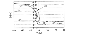
本実施例では、上記実施の形態1に基づき大気下でベークし作製した有機TFTの電気特性の温度依存性を測定した結果を示す。なお測定試料の有機TFTは、図3に示すように大気中において石英基板上にタングステンからなるゲート電極301を設け、ゲート電極上にゲート絶縁膜を設け、ゲート絶縁膜上にタングステンからなるソース電極302とドレイン電極303を設け、ソース電極302とドレイン電極303との間に有機半導体膜が設けられている構造である。そして、各ソース電極302、ドレイン電極303、ゲート電極301には測定電圧を印加したり、電流を検出したりするための測定用パッド(ソース電極用パッド304、ドレイン電極用パッド305、ゲート電極用パッド306)が設けられている。
In this example, the results of measuring the temperature dependence of the electrical characteristics of an organic TFT fabricated by baking in the atmosphere based on the first embodiment will be shown. As shown in FIG. 3, the organic TFT of the measurement sample is provided with a
また、有機TFTのチャネル長はソース電極とドレイン電極との間(図3においてLで示す)の長さで与えられ、Lは5μmであり、チャネル幅はソース電極とドレイン電極とが重なる領域の長さ(図3においてWで示す)で与えられ、Wは8000μmである。 The channel length of the organic TFT is given by the length between the source electrode and the drain electrode (indicated by L in FIG. 3), L is 5 μm, and the channel width is the region where the source electrode and the drain electrode overlap. It is given by the length (indicated by W in FIG. 3), and W is 8000 μm.
また有機半導体の材料はペンタセンを用い、膜厚は50nmで成膜した。成膜方法としては蒸着法を用いた。 The organic semiconductor material was pentacene and the film thickness was 50 nm. A vapor deposition method was used as a film forming method.
蒸着後のベーク条件は、以下のとおりである。
(1)ベークなし
(2)大気下において、120℃で、10分ベーク
(3)大気下において、150℃で、10分ベーク
(4)大気下において、200℃で、10分ベーク
(5)大気下において、250℃で、10分ベーク
The baking conditions after vapor deposition are as follows.
(1) No baking (2) Bake for 10 minutes at 120 ° C in air (3) Bake for 10 minutes at 150 ° C in air (4) Bake for 10 minutes at 200 ° C in air (5) Bake at 250 ° C for 10 minutes in air
図4にはベーク条件(1)〜(5)におけるVdとして−10Vの電圧を印加したときの、ドレイン電極の電流とゲート電圧とを測定したVg−Id特性の結果を示す。 FIG. 4 shows the results of Vg-Id characteristics obtained by measuring the drain electrode current and the gate voltage when a voltage of −10 V is applied as Vd under baking conditions (1) to (5).
図4より、蒸着後のベークによって、オンオフの閾値が0Vに近づいていることが分かり、大気下においては、(2)120℃10分より(3)150℃10分の方が、閾値のシフトが大きく、(3)150℃10分と(4)200℃10分では余り変化が無いことが分かる。また、図4より、蒸着ベークによって、オフ時のリーク電流が減っていることが分かる。この変化も(2)120℃10分より(3)150℃10分、(3)150℃10分より(4)200℃10分の方が大きいことが分かる。これは、ベークすることにより有機半導体膜中に含まれる水分が減少するため有機半導体膜の劣化が抑えられることにより、ベーク前に比べてTFT特性が改善していると推測される。また、ベークすることによりソース電極またはドレイン電極および絶縁膜と有機半導体膜との密着性が向上し、有機半導体膜の結晶性の向上、キャリア輸送性の向上が図られるため、ベーク前に比べてTFT特性が改善していると推測される。さらに、高温のほうが、より有機半導体膜とソース電極またはドレイン電極および絶縁膜との密着性が向上し、TFT特性の改善に効果的であると推測される。 From FIG. 4, it can be seen that the on / off threshold approaches 0 V due to baking after vapor deposition. In the atmosphere, the threshold shift is greater at (3) 150 ° C. for 10 minutes than (2) 120 ° C. for 10 minutes. It can be seen that (3) 150 ° C. for 10 minutes and (4) 200 ° C. for 10 minutes do not change much. Moreover, FIG. 4 shows that the leakage current at the time of OFF has decreased by vapor deposition baking. It can be seen that (2) 120 ° C. for 10 minutes is also larger (3) 150 ° C. for 10 minutes, and (3) 150 ° C. for 10 minutes than (4) 200 ° C. for 10 minutes. This is presumed that the TFT characteristics are improved as compared with those before baking because the moisture contained in the organic semiconductor film is reduced by baking and the deterioration of the organic semiconductor film is suppressed. Baking improves the adhesion between the source or drain electrode and the insulating film and the organic semiconductor film, and improves the crystallinity of the organic semiconductor film and the carrier transportability. It is estimated that the TFT characteristics are improved. Further, it is presumed that the higher temperature improves the adhesion between the organic semiconductor film and the source or drain electrode and the insulating film, and is effective in improving the TFT characteristics.
以上から、蒸着後のベークは有機TFTの特性改善に有効であると考えられる。 From the above, it is considered that baking after vapor deposition is effective in improving the characteristics of the organic TFT.
また(5)250℃10分でベークする場合、有機TFTの特性の改善が見られなかった。250℃近傍から、ペンタセンが熱分解や酸化してしまい、有機TFTの特性消失したと考えられる。そのため、有機半導体材料としてペンタセンを用いた場合、加熱温度は250℃未満がよいことが分かる。 Moreover, (5) When baking at 250 degreeC for 10 minutes, the improvement of the characteristic of organic TFT was not seen. It is considered that pentacene is thermally decomposed and oxidized from around 250 ° C., and the characteristics of the organic TFT are lost. Therefore, it can be seen that when pentacene is used as the organic semiconductor material, the heating temperature is preferably less than 250 ° C.
本実施例では、上記実施の形態1に基づき大気下でベークし作製した有機TFTの電気特性の時間依存性を測定した結果を示す。なお測定試料である有機TFTの蒸着後ベーク以外の作製条件は、実施例1と同様である。 In this example, the results of measuring the time dependence of the electrical characteristics of an organic TFT fabricated by baking in the atmosphere based on the first embodiment will be shown. The production conditions other than the post-deposition baking of the organic TFT as the measurement sample are the same as in Example 1.
蒸着後のベーク条件は、以下のとおりである。
(1)蒸着後のベーク前
(2)(1)を大気下において、120℃で、10分ベーク
(3)(2)をさらに大気下において、120℃で、30分ベーク
The baking conditions after vapor deposition are as follows.
(1) After baking (2) Before baking (1) under the atmosphere at 120 ° C. for 10 minutes Baking (3) (2) under the atmosphere at 120 ° C. for 30 minutes
図5にはベーク条件(1)〜(3)におけるVdとして−10Vの電圧を印加したときの、ドレイン電極の電流とゲート電圧とを測定したVg−Id特性の結果を示す。 FIG. 5 shows the results of Vg-Id characteristics obtained by measuring the drain electrode current and the gate voltage when a voltage of −10 V is applied as Vd under the baking conditions (1) to (3).
図5より、蒸着後のベークによって、オンオフの閾値が0Vに近づいていることがわかり、ベークする時間が長いほど大きくシフトしていることが分かる。これは、ベークすることにより有機半導体膜中に含まれる水分が減少するため有機半導体膜の劣化が抑えられることにより、ベーク前に比べてTFT特性が改善していると推測される。また、ベークすることにより電極および絶縁膜と有機半導体膜との密着性が向上し、有機半導体層の結晶性の向上、キャリア輸送性の向上が図られるため、ベーク前に比べてTFT特性が改善していると推測される。さらに、長時間ベークすることにより、有機半導体膜中の水分の減少および電極および絶縁膜と有機半導体膜との密着性の向上が促進され、有機半導体の特性の改善に高い効果を示していると推測される。
以上から、蒸着後のベークは有機TFTの特性改善に有効であると考えられる。
From FIG. 5, it can be seen that the on / off threshold approaches 0 V due to baking after deposition, and that the longer the baking time, the greater the shift. This is presumed that the TFT characteristics are improved as compared with those before baking because the moisture contained in the organic semiconductor film is reduced by baking and the deterioration of the organic semiconductor film is suppressed. In addition, baking improves the adhesion between the electrode and insulating film and the organic semiconductor film, improves the crystallinity of the organic semiconductor layer, and improves the carrier transportability, thus improving TFT characteristics compared to before baking. Presumed to be. Furthermore, baking for a long time promotes the reduction of moisture in the organic semiconductor film and the enhancement of adhesion between the electrode and insulating film and the organic semiconductor film, and shows a high effect in improving the characteristics of the organic semiconductor. Guessed.
From the above, it is considered that baking after vapor deposition is effective in improving the characteristics of the organic TFT.
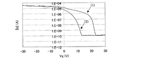
本実施例では、上記実施の形態1に基づき、蒸着後一旦大気圧に開放してから減圧下(1.2×10⁴Pa)でベークし作製した有機TFTの電気特性の温度依存性を測定した結果を示す。なお測定試料である有機TFTの蒸着後ベーク以外の作製条件は、実施例1と同様である。 In this example, based on the first embodiment, the temperature dependence of the electrical characteristics of an organic TFT prepared by baking to atmospheric pressure after deposition and baking under reduced pressure (1.2 × 10 4 Pa) was measured. The results are shown. The production conditions other than the post-deposition baking of the organic TFT as the measurement sample are the same as in Example 1.
ベーク条件は、以下のとおりである。
(1)減圧下(1.2×10⁴Pa)において、120℃で、10分ベーク
(2)減圧下(1.2×10⁴Pa)において、150℃で、10分ベーク
(3)減圧下(1.2×10⁴Pa)において、200℃で、10分ベーク
The baking conditions are as follows.
(1) Bake for 10 minutes at 120 ° C. under reduced pressure (1.2 × 10 4 Pa) (2) Bake for 10 minutes at 150 ° C. under reduced pressure (1.2 × 10 4 Pa) (3) Reduced pressure Bake at 200 ° C for 10 minutes under (1.2 x 10 4 Pa)
図6にはベーク条件(1)〜(3)におけるVdとして−10Vの電圧を印加したときの、ドレイン電極の電流とゲート電圧とを測定したVg−Id特性の結果を示す。 FIG. 6 shows the results of Vg-Id characteristics obtained by measuring the drain electrode current and the gate voltage when a voltage of −10 V is applied as Vd under the baking conditions (1) to (3).
図6より、蒸着後のベークによって、オンオフの閾値が0Vに近づいていることが分かり、減圧下(1.2×104Pa)においては、(1)120℃10分より(2)150℃10分の方が、閾値のシフトが大きいことが分かる。また、図6より、蒸着ベークによって、オフ時のリーク電流が減っていることが分かる。この変化も(1)120℃10分より(2)150℃10分の方が大きいことが分かる。また上記実施例1で行なった大気下でのベークと比べ、スロープの立ち上がりが急峻なことから良好なS値が得られていることが分かる。これは実施例1と同様に、ベークすることにより、有機半導体膜中に含まれる水分が減少するため有機半導体膜の劣化が抑えられ、TFT特性が改善していると推測される。また、ベークすることによりソース電極またはドレイン電極および絶縁膜と有機半導体膜との密着性が向上し、有機半導体膜の結晶性の向上、キャリア輸送性の向上が図られるため、TFT特性が改善していると推測される。さらに、高温のほうが、より有機半導体膜とソース電極またはドレイン電極および絶縁膜との密着性が向上し、TFT特性の改善に高い効果を示していると推測される。本実施例ではさらに、減圧下でベークすることにより、大気中の酸素の影響による有機半導体膜の酸化などの劣化が抑えられるため、大気圧下でのベークに比べてTFT特性が改善していると推測される。 From FIG. 6, it can be seen that the on / off threshold approaches 0 V by baking after vapor deposition. Under reduced pressure (1.2 × 10 4 Pa), (2) 150 ° C. from (1) 120 ° C. for 10 minutes. It can be seen that the threshold shift is larger at 10 minutes. Further, it can be seen from FIG. 6 that the leakage current at the time of OFF is reduced by the vapor deposition baking. It can be seen that this change is also larger at (2) 150 ° C. for 10 minutes than (1) 120 ° C. for 10 minutes. It can also be seen that a favorable S value is obtained because the slope rises more steeply than the bake in the atmosphere performed in Example 1 above. In the same manner as in Example 1, it is presumed that by baking, the moisture contained in the organic semiconductor film decreases, so that the deterioration of the organic semiconductor film is suppressed and the TFT characteristics are improved. In addition, baking improves the adhesion between the source or drain electrode and the insulating film and the organic semiconductor film, improves the crystallinity of the organic semiconductor film, and improves the carrier transportability, thereby improving the TFT characteristics. I guess that. Further, it is presumed that the higher the temperature, the higher the adhesion between the organic semiconductor film and the source or drain electrode and the insulating film, and the higher the TFT characteristics. Further, in this embodiment, the baking is performed under reduced pressure, so that deterioration such as oxidation of the organic semiconductor film due to the influence of oxygen in the atmosphere can be suppressed. Therefore, TFT characteristics are improved as compared with baking at atmospheric pressure. It is guessed.
以上から、蒸着後のベークは有機TFTの特性改善に有効であって、更に減圧下でベークを行うと温度の低温化を図ることができると考えられる。 From the above, it is considered that baking after vapor deposition is effective for improving the characteristics of the organic TFT, and that the temperature can be lowered by further baking under reduced pressure.
本実施例では、上記実施の形態1に基づき、蒸着後一旦大気圧に開放してから減圧下(1.2×10⁴Pa)でベークし作製した有機TFTの電気特性の大気中放置による経時変化と、その後の減圧下(1.2×10⁴Pa)ベークの効果を評価した。以下に結果を示す。なお測定試料である有機TFTの蒸着後ベーク以外の作製条件は、実施例1と同様である。
In this example, the electrical characteristics of the organic TFT produced by evacuation under a reduced pressure (1.2 × 10 4 Pa) after being temporarily released to atmospheric pressure after vapor deposition based on the above-described
ベーク条件は、以下のとおりである。
(1)減圧下(1.2×10⁴Pa)において、150℃で、30分ベーク
(2)(1)を大気下において48時間放置
(3)(2)を減圧下(1.2×10⁴Pa)において、150℃で、30分ベーク
The baking conditions are as follows.
(1) Bake for 30 minutes at 150 ° C. under reduced pressure (1.2 × 10 4 Pa) (2) Leave (1) in air for 48 hours (3) (2) under reduced pressure (1.2 × 10 4 Pa) at 150 ° C. for 30 minutes
図7にはベーク条件(1)〜(3)におけるVdとして−10Vの電圧を印加したときの、ドレイン電極の電流とゲート電圧とを測定したVg−Id特性の結果を示す。 FIG. 7 shows the results of Vg-Id characteristics obtained by measuring the drain electrode current and the gate voltage when a voltage of −10 V is applied as Vd under the baking conditions (1) to (3).
図7より蒸着後のベークによって、オンオフの閾値が0Vに近づいていることが分かり、大気下で48時間放置することによりON電流が減少しTFT特性が劣化していることが分かる。またその後再びベークすることでON電流が上昇し、有機TFT特性が回復していることが分かる。これは、実施例4と同様に、ベークすることにより有機半導体膜中に含まれる水分が減少するため有機半導体膜の劣化が抑えられることにより、TFT特性が改善していると推測される。また、ベークすることによりソース電極またはドレイン電極および絶縁膜と有機半導体膜との密着性が向上し、有機半導体膜の結晶性の向上、キャリア輸送性の向上が図られるため、TFT特性が改善していると推測される。さらに、減圧下でベークすることにより、大気中の酸素の影響による有機半導体膜の酸化などの劣化が抑えられるため、TFT特性が改善していると推測される。 From FIG. 7, it can be seen that the ON / OFF threshold approaches 0 V by baking after deposition, and that the ON current decreases and the TFT characteristics deteriorate when left in the atmosphere for 48 hours. Moreover, it turns out that ON current rises by baking again after that and the organic TFT characteristic has recovered | restored. This is presumed that the TFT characteristics are improved by suppressing the deterioration of the organic semiconductor film because the moisture contained in the organic semiconductor film is reduced by baking as in the case of Example 4. In addition, baking improves the adhesion between the source or drain electrode and the insulating film and the organic semiconductor film, improves the crystallinity of the organic semiconductor film, and improves the carrier transportability, thereby improving the TFT characteristics. I guess that. Furthermore, by baking under reduced pressure, deterioration of the organic semiconductor film due to the influence of oxygen in the atmosphere can be suppressed, and it is assumed that the TFT characteristics are improved.
以上から、蒸着後のベークは有機TFTの特性の大気下放置による劣化を回復するのに有効であると考えられる。 From the above, it is considered that baking after vapor deposition is effective in recovering the deterioration of the characteristics of the organic TFT due to being left in the atmosphere.
本実施例では、上記実施の形態1に基づき、蒸着直後に蒸着チャンバー内でベークし作製した有機TFTの電気特性を測定した結果を示す。なお測定試料である有機TFTの蒸着後ベーク以外の作製条件は、実施例1と同様である。 In this example, the results of measuring the electrical characteristics of an organic TFT produced by baking in a vapor deposition chamber immediately after vapor deposition based on the first embodiment are shown. The production conditions other than the post-deposition baking of the organic TFT as the measurement sample are the same as in Example 1.
蒸着後のベーク条件は、蒸着チャンバー内で行なっているので、蒸着時と同じ減圧下(1.3×10⁻³Pa)において行なった。ベーク条件は、以下のとおりである。
(1)ベークなし
(2)120℃で、10分ベーク
Since the baking conditions after the vapor deposition were performed in the vapor deposition chamber, they were performed under the same reduced pressure (1.3 × 10 −3 Pa) as that during the vapor deposition. The baking conditions are as follows.
(1) No baking (2) Bake at 120 ° C for 10 minutes
図8にはベーク条件(1)、(2)におけるVdとして−10Vの電圧を印加したときの、ドレイン電極の電流とゲート電圧とを測定したVg−Id特性の結果を示す。 FIG. 8 shows the results of Vg-Id characteristics obtained by measuring the drain electrode current and the gate voltage when a voltage of −10 V is applied as Vd in the baking conditions (1) and (2).
図8より、蒸着チャンバー内での蒸着後ベークによって、オンオフの閾値が0Vに近づいており、TFT特性を改善していることが分かる。これは、ベークすることにより有機半導体膜中に含まれる水分が減少するため有機半導体膜の劣化が抑えられることにより、ベーク前に比べてTFT特性が改善していると推測される。また、ベークすることによりソース電極またはドレイン電極および絶縁膜と有機半導体膜との密着性が向上し、有機半導体膜の結晶性の向上、キャリア輸送性の向上が図られるため、ベーク前に比べてTFT特性が改善していると推測される。 From FIG. 8, it can be seen that the on / off threshold approaches 0 V due to post-deposition baking in the deposition chamber, which improves the TFT characteristics. This is presumed that the TFT characteristics are improved as compared with those before baking because the moisture contained in the organic semiconductor film is reduced by baking and the deterioration of the organic semiconductor film is suppressed. Baking improves the adhesion between the source or drain electrode and the insulating film and the organic semiconductor film, and improves the crystallinity of the organic semiconductor film and the carrier transportability. It is estimated that the TFT characteristics are improved.
以上から、蒸着チャンバー内での蒸着後ベークは有機TFTの特性改善に有効であると考えられる。 From the above, it is considered that post-deposition baking in the deposition chamber is effective for improving the characteristics of the organic TFT.
本実施例では、蒸着後のベークによるペンタセンの粒界の大きさと有機層の膜厚の変化をAFMで測定した結果を示す。なお測定試料は、実施例1と同様に基板上にペンタセンを膜厚50nmで成膜した。成膜方法としては、蒸着法を用いた。 In this example, the results of measuring the change in the size of the grain boundary of pentacene and the film thickness of the organic layer by baking after vapor deposition are shown by AFM. The measurement sample was formed by depositing pentacene with a film thickness of 50 nm on the substrate in the same manner as in Example 1. A vapor deposition method was used as a film forming method.
測定試料の条件は、以下のとおりである。
(1)蒸着後ベークなし
(2)蒸着後に減圧下(1.2×10⁴Pa)において、150℃で、10分ベーク
The conditions of the measurement sample are as follows.
(1) No baking after vapor deposition (2) Bake for 10 minutes at 150 ° C. under reduced pressure (1.2 × 10 4 Pa) after vapor deposition
図9には条件(1)、図10に条件(2)におけるAFMの測定結果を示す。 FIG. 9 shows the AFM measurement results under the condition (1) and FIG. 10 shows the conditions (2).
図9,10より、蒸着後のベークによって、ベークの有無でペンタセンの粒界の大きさの変化は見られないことがわかる。またこのとき、有機膜の膜厚の変化も見られなかった。 9 and 10, it can be seen that no change in the size of the grain boundary of pentacene is observed with or without baking after baking. At this time, no change in the thickness of the organic film was observed.
以上の結果より、有機半導体膜を形成後、加熱する温度は、有機半導体が結晶成長しない温度、好ましくは有機半導体膜の粒界の大きさの平均値が10%以上成長しない温度でよいことがわかる。 From the above results, the heating temperature after forming the organic semiconductor film may be a temperature at which the organic semiconductor does not grow, preferably a temperature at which the average value of the grain boundary of the organic semiconductor film does not grow more than 10%. Recognize.
(実施の形態3)
本発明の半導体装置を含む液晶装置の態様について、図11を用いて説明する。なお、液晶装置の構成について特に限定は無く、本形態で示した態様の他、例えば、素子基板上に、駆動回路が設けられたものであってもよい。また、液晶装置に限定されるものではなく、発光素子を有する表示装置のスイッチング素子等に本発明の有機半導体装置を用いても良い。
(Embodiment 3)
A mode of a liquid crystal device including the semiconductor device of the present invention will be described with reference to FIGS. Note that there is no particular limitation on the structure of the liquid crystal device, and a driving circuit may be provided over an element substrate, for example, in addition to the embodiment described in this embodiment. In addition, the organic semiconductor device of the present invention may be used as a switching element of a display device having a light emitting element without being limited to the liquid crystal device.
図11は液晶装置を模式的に表した上面図である。本形態の液晶装置は、素子基板1101と対向基板1102とが対向するように貼り合わせられている。本形態の液晶装置は、画素部1103を有する。そして、画素部1103の一端に沿うように設けられた端子部1104には、フレキシブルプリント配線(FPC)1105が装着され、フレキシブルプリント配線1105を介して駆動回路から画素部1103に信号が入力される。なお、本形態のように、駆動回路とフレキシブルプリント配線とは独立して設けられていてもよいし、または配線パターンが形成されたFPC上にICチップが実装されたTCP等の様に複合していてもよい。
FIG. 11 is a top view schematically showing the liquid crystal device. In the liquid crystal device of this embodiment mode, the
画素部1103について特に限定はなく、例えば図12(A)または図12(B)の断面図で表されるように、液晶素子とそれを駆動するためのトランジスタとを含む。図12(A)と図12(B)とは、それぞれ、液晶装置の断面構造の態様であり、含まれるトランジスタの構造が異なる。ただし、本発明を用いたトランジスタの構造及び形成方法は、本実施の形態に限定されず様々な形態が可能である。
The
図12(A)の断面図で表される液晶装置は、有機半導体膜524の上にソースまたはドレインとして機能する電極525、526を有するトランジスタ527が設けられた素子基板521を有する。
The liquid crystal device illustrated in the cross-sectional view of FIG. 12A includes an
また、画素電極529と対向電極532との間に液晶層534を挟んでいる。画素電極529と対向電極532の材料としては、インジウム錫酸化物(ITO)、酸化ケイ素を含むインジウム錫酸化物(ITSO)等の透光性材料が挙げられる。また、画素電極529の材料として、アルミニウム(Al)、銀(Ag)等の反射性の高い導電性材料を用いても良い。画素電極529に透過性材料を用いた場合、透過型液晶パネルが形成され、画素電極529の全面が反射性の高い導電性材料で形成された場合、反射型液晶表示装置が形成される。さらに、画素電極529の一部に透過性材料、残りの部分に反射性の高い導電性材料を用いて半透過型液晶表示装置を形成しても良い。
In addition, a
画素電極529、対向電極532のそれぞれにおいて液晶層534と接する側の表面には、配向膜530、533が設けられている。液晶層534には、スペーサ535が分散し、セルギャップを保っている。
トランジスタ527は、コンタクトホールが設けられた絶縁層528によって覆われており、電極526と画素電極529とは電気的に接続している。絶縁層528は、テフロン(登録商標)を用いたスパッタ法やプラズマCVD法等で形成すればよい。また、有機半導体膜の劣化を抑えるために、SiN、SiO2、SiON等を用いた熱CVD法により形成してもよい。
The
ここで、対向電極532は、対向基板531によって支持されている。また、トランジスタ527において、有機半導体膜524とゲート電極522とは、間にゲート絶縁層523を挟んで重畳している。
Here, the
また、図12(B)の断面図で表される液晶装置は、ソースまたはドレインとして機能する電極555、554の少なくとも一部が有機半導体膜556によって覆われた構造を有するトランジスタ557を含む素子基板551を有する。また、画素電極559と対向電極562との間に液晶層564を挟んでいる。画素電極559、対向電極562のそれぞれにおいて液晶層564と接する側の表面には、配向膜560、563が設けられている。液晶層564には、スペーサ565が分散し、セルギャップを保っている。
In addition, the liquid crystal device illustrated in the cross-sectional view of FIG. 12B includes an element substrate including a
トランジスタ557は、コンタクトホールが設けられた絶縁層558a、558bによって覆われており、電極554と画素電極559とは電気的に接続している。なお、トランジスタを覆う絶縁層は、図12(B)のように絶縁層558aと絶縁層558bとから成る多層であってもよいし、図12(A)のように絶縁層528からなる単層であってもよい。また、トランジスタを覆う絶縁層は、図12(B)の絶縁層558bのように表面が平坦化された層であってもよい。ここで、絶縁層528aは図12(A)の絶縁層528と同様に形成すればよい。絶縁層528bは、スピンコート法によりアクリル、ポリイミド、ポリイミドアミド等の有機物で形成してもよいし、ポジ型又はネガ型の感光性樹脂を用いて形成してもよい。
The
ここで、対向電極562は、対向基板561によって支持されている。また、トランジスタ557において、有機半導体膜556とゲート電極552とは、間にゲート絶縁層553を挟んで重畳している。
Here, the
(実施の形態4)
以上のような表示装置は、図13(A)、(B)、(C)に示すように、携帯電話機や、テレビ受像機等に実装される表示装置として用いることができる。IDカードの様な個人情報を管理する機能を有するカード等に実装してもよい。また、本発明の利用形態は図13に示した例に限定されず、様々な電子機器に利用することが可能である。
(Embodiment 4)
As shown in FIGS. 13A, 13B, and 13C, the display device as described above can be used as a display device mounted on a mobile phone, a television receiver, or the like. You may mount in the card etc. which have a function which manages personal information like an ID card. Further, the usage form of the present invention is not limited to the example shown in FIG. 13 and can be used for various electronic devices.
図13(A)は携帯電話機の図であり、本体1302には表示部1301と、音声出力部1304、音声入力部1305、操作スイッチ1306、1307、アンテナ1303等によって構成されている。この携帯電話機は、動作特性が良く、信頼性の高いものである。本発明の有機半導体装置を表示部1301に組み込むことでこのような携帯電話機を完成できる。
FIG. 13A illustrates a cellular phone. A
図13(B)は、本発明を適用して作製したテレビ受像機であり、表示部1311、筐体1312、スピーカー1313などによって構成されている。このテレビ受像機は、動作特性が良く、信頼性の高いものである。本発明の有機半導体装置を表示部1311に組み込むことでこのようなテレビ受像機を完成できる。
FIG. 13B illustrates a television set manufactured by applying the present invention, which includes a
図13(C)は、本発明を適用して作製したIDカードであり、支持体1321、表示部1322、支持体1321内に組み込まれた集積回路チップ1323等によって構成されている。なお、表示部1322を駆動するための集積回路1324、1325についても支持体1321内に組み込まれている。このIDカードは、信頼性の高いものである。また、例えば、表示部1322において、集積回路チップ1323において入出力された情報を表示し、どのような情報が入出力されたかを確認することができる。本発明の有機半導体装置を表示部1322に組み込むことでこのようなIDカードを完成できる。
FIG. 13C illustrates an ID card manufactured by applying the present invention, which includes a support 1321, a
100 基板
101 ゲート電極
102 ゲート絶縁膜
103 ソースまたはドレイン電極
104 有機半導体膜
110 素子基板
200 基板
201 ゲート電極
202 ゲート絶縁膜
203 有機半導体膜
204 電極
210 素子基板
301 ゲート電極
302 ソース電極
303 ドレイン電極
304 ソース電極用パッド
305 ドレイン電極用パッド
306 ゲート電極用パッド
1101 素子基板
1102 対向基板
1103 画素部
1104 端子部
1105 フレキシブルプリント配線
521 素子基板
522 ゲート電極
523 ゲート絶縁層
524 有機半導体膜
525 電極
526 電極
527 トランジスタ
528 絶縁層
529 画素電極
530 配向膜
531 対向基板
532 対向電極
533 配向膜
534 液晶層
535 スペーサ
551 素子基板
552 ゲート電極
553 ゲート絶縁層
554 電極
555 電極
556 有機半導体膜
557 トランジスタ
558a 絶縁層
558b 絶縁層
559 画素電極
560 配向膜
561 対向基板
562 対向電極
563 配向膜
564 液晶層
565 スペーサ
1301 表示部
1302 本体
1303 アンテナ
1304 音声出力部
1305 音声入力部
1306 操作スイッチ
1307 操作スイッチ
1311 表示部
1312 筐体
1313 スピーカー
1321 支持体
1322 表示部
1323 集積回路チップ
1324 集積回路
1325 集積回路
100
Claims (8)
真空蒸着法により、前記ゲート電極上に有機半導体膜を形成し、
前記有機半導体膜を減圧下で加熱して前記有機半導体膜を大気中に放置後、減圧下で加熱し、
前記加熱された有機半導体膜上にソース電極及びドレイン電極を形成することを特徴とする有機半導体素子の作製方法。 Forming a gate electrode,
An organic semiconductor film is formed on the gate electrode by vacuum deposition,
The organic semiconductor film is heated under reduced pressure and the organic semiconductor film is left in the atmosphere , and then heated under reduced pressure .
A method for manufacturing an organic semiconductor element, comprising forming a source electrode and a drain electrode on the heated organic semiconductor film.
前記ゲート電極上にソース電極及びドレイン電極を形成し、
真空蒸着法により、前記ソース電極及びドレイン電極上に有機半導体膜を形成し、
前記有機半導体膜を減圧下で加熱して前記有機半導体膜を大気中に放置後、減圧下で加熱することを特徴とする有機半導体素子の作製方法。 Forming a gate electrode,
Forming a source electrode and a drain electrode on the gate electrode;
An organic semiconductor film is formed on the source and drain electrodes by vacuum deposition,
A method for manufacturing an organic semiconductor element, wherein the organic semiconductor film is heated under reduced pressure, the organic semiconductor film is left in the atmosphere , and then heated under reduced pressure .
前記減圧下、かつ不活性ガス雰囲気において、前記有機半導体膜を加熱することを特徴とする有機半導体素子の作製方法。 In claim 1 or claim 2,
A method for manufacturing an organic semiconductor element, comprising heating the organic semiconductor film under the reduced pressure and in an inert gas atmosphere.
真空蒸着法により、前記ゲート電極上に有機半導体膜を形成し、
前記有機半導体膜を減圧下で加熱して前記有機半導体膜を大気中に放置後、大気圧下で加熱し、
前記加熱された有機半導体膜上にソース電極及びドレイン電極を形成することを特徴とする有機半導体素子の作製方法。 Forming a gate electrode,
An organic semiconductor film is formed on the gate electrode by vacuum deposition,
The organic semiconductor film by heating under reduced pressure the organic semiconductor film after being left in the atmosphere, and heated at atmospheric pressure,
A method for manufacturing an organic semiconductor element, comprising forming a source electrode and a drain electrode on the heated organic semiconductor film.
前記ゲート電極上にソース電極及びドレイン電極を形成し、
真空蒸着法により、前記ソース電極及びドレイン電極上に有機半導体膜を形成し、
前記有機半導体膜を減圧下で加熱して前記有機半導体膜を大気中に放置後、大気圧下で加熱することを特徴とする有機半導体素子の作製方法。 Forming a gate electrode,
Forming a source electrode and a drain electrode on the gate electrode;
An organic semiconductor film is formed on the source and drain electrodes by vacuum deposition,
A method for manufacturing an organic semiconductor element, comprising: heating the organic semiconductor film under reduced pressure , allowing the organic semiconductor film to stand in the atmosphere , and then heating the organic semiconductor film under atmospheric pressure .
前記有機半導体膜を加熱するときは、前記有機半導体膜の融点未満で加熱することを特徴とする有機半導体素子の作製方法。 In any one of Claims 1 thru | or 5 ,
Wherein when heating the organic semiconductor film, a manufacturing method of an organic semiconductor element characterized in that heating below the melting point of the organic semiconductor film.
前記有機半導体膜を加熱するときは、250℃未満で加熱することを特徴とする有機半導体素子の作製方法。 In any one of Claims 1 thru | or 6 ,
Wherein when heating the organic semiconductor film, a manufacturing method of an organic semiconductor device, which comprises heating at less than 250 ° C..
前記有機半導体膜を加熱するときは、前記有機半導体膜の粒界の大きさの平均値が10%以上成長しない温度で加熱することを特徴とする有機半導体素子の作製方法。 In any one of Claims 1 thru | or 7 ,
Wherein when heating the organic semiconductor film, a manufacturing method of an organic semiconductor device having an average value of the grain boundaries of the size of the organic semiconductor film is characterized by heating at a temperature not grow more than 10%.
Priority Applications (1)
| Application Number | Priority Date | Filing Date | Title |
|---|---|---|---|
| JP2004359575A JP4877869B2 (en) | 2003-12-26 | 2004-12-13 | Method for producing organic semiconductor element |
Applications Claiming Priority (3)
| Application Number | Priority Date | Filing Date | Title |
|---|---|---|---|
| JP2003434620 | 2003-12-26 | ||
| JP2003434620 | 2003-12-26 | ||
| JP2004359575A JP4877869B2 (en) | 2003-12-26 | 2004-12-13 | Method for producing organic semiconductor element |
Publications (3)
| Publication Number | Publication Date |
|---|---|
| JP2005210087A JP2005210087A (en) | 2005-08-04 |
| JP2005210087A5 JP2005210087A5 (en) | 2007-11-08 |
| JP4877869B2 true JP4877869B2 (en) | 2012-02-15 |
Family
ID=34914336
Family Applications (1)
| Application Number | Title | Priority Date | Filing Date |
|---|---|---|---|
| JP2004359575A Expired - Fee Related JP4877869B2 (en) | 2003-12-26 | 2004-12-13 | Method for producing organic semiconductor element |
Country Status (1)
| Country | Link |
|---|---|
| JP (1) | JP4877869B2 (en) |
Families Citing this family (5)
| Publication number | Priority date | Publication date | Assignee | Title |
|---|---|---|---|---|
| JP2007096129A (en) * | 2005-09-29 | 2007-04-12 | Kyoto Univ | Molecule transistor, and method for manufacturing the same and nonvolatile memory and piezoelectric sensor using the same method |
| JP5380831B2 (en) * | 2007-12-07 | 2014-01-08 | 株式会社リコー | Organic transistor and manufacturing method thereof |
| JP2010199099A (en) * | 2009-02-20 | 2010-09-09 | Univ Of Tokyo | Method of controlling threshold voltage in organic electric field effect transistor |
| JP2010199100A (en) * | 2009-02-20 | 2010-09-09 | Univ Of Tokyo | Method of manufacturing organic semiconductor element |
| JP5733612B2 (en) * | 2011-03-08 | 2015-06-10 | 国立大学法人信州大学 | Material for organic semiconductor thin film, method of forming organic semiconductor thin film using the material, and organic thin film transistor |
Family Cites Families (1)
| Publication number | Priority date | Publication date | Assignee | Title |
|---|---|---|---|---|
| US5574291A (en) * | 1994-12-09 | 1996-11-12 | Lucent Technologies Inc. | Article comprising a thin film transistor with low conductivity organic layer |
-
2004
- 2004-12-13 JP JP2004359575A patent/JP4877869B2/en not_active Expired - Fee Related
Also Published As
| Publication number | Publication date |
|---|---|
| JP2005210087A (en) | 2005-08-04 |
Similar Documents
| Publication | Publication Date | Title |
|---|---|---|
| US8202760B2 (en) | Method for manufacturing an organic semiconductor element | |
| JP5412458B2 (en) | Method for manufacturing semiconductor device | |
| US7732248B2 (en) | Manufacturing method of semiconductor device | |
| US8742409B2 (en) | Thin film transistor and method for producing the same | |
| JP5025110B2 (en) | Method for manufacturing semiconductor device | |
| JP5477750B2 (en) | Organic field effect transistor | |
| JP4836446B2 (en) | Method for manufacturing semiconductor device | |
| US9634271B2 (en) | Semiconductor device, method of manufacturing the same, and electronic apparatus | |
| JP4856900B2 (en) | Method for manufacturing field effect transistor | |
| JP2009176828A (en) | Thin film transistor, matrix substrate, electrophoresis display device, and electronic apparatus | |
| JP4877869B2 (en) | Method for producing organic semiconductor element | |
| JP4419425B2 (en) | Organic thin film transistor element | |
| JP5029938B2 (en) | Electrophoretic display device, electronic apparatus, and method of manufacturing electrophoretic display device | |
| US20130193413A1 (en) | Stacking structure, organic semiconductor device, wiring, and display, and method of manufacturing organic semiconductor device |
Legal Events
| Date | Code | Title | Description |
|---|---|---|---|
| A521 | Request for written amendment filed |
Free format text: JAPANESE INTERMEDIATE CODE: A523 Effective date: 20070925 |
|
| A621 | Written request for application examination |
Free format text: JAPANESE INTERMEDIATE CODE: A621 Effective date: 20070925 |
|
| A977 | Report on retrieval |
Free format text: JAPANESE INTERMEDIATE CODE: A971007 Effective date: 20110222 |
|
| A131 | Notification of reasons for refusal |
Free format text: JAPANESE INTERMEDIATE CODE: A131 Effective date: 20110315 |
|
| A521 | Request for written amendment filed |
Free format text: JAPANESE INTERMEDIATE CODE: A523 Effective date: 20110405 |
|
| A131 | Notification of reasons for refusal |
Free format text: JAPANESE INTERMEDIATE CODE: A131 Effective date: 20111004 |
|
| A521 | Request for written amendment filed |
Free format text: JAPANESE INTERMEDIATE CODE: A523 Effective date: 20111102 |
|
| TRDD | Decision of grant or rejection written | ||
| A01 | Written decision to grant a patent or to grant a registration (utility model) |
Free format text: JAPANESE INTERMEDIATE CODE: A01 Effective date: 20111122 |
|
| A01 | Written decision to grant a patent or to grant a registration (utility model) |
Free format text: JAPANESE INTERMEDIATE CODE: A01 |
|
| A61 | First payment of annual fees (during grant procedure) |
Free format text: JAPANESE INTERMEDIATE CODE: A61 Effective date: 20111123 |
|
| R150 | Certificate of patent or registration of utility model |
Ref document number: 4877869 Country of ref document: JP Free format text: JAPANESE INTERMEDIATE CODE: R150 Free format text: JAPANESE INTERMEDIATE CODE: R150 |
|
| FPAY | Renewal fee payment (event date is renewal date of database) |
Free format text: PAYMENT UNTIL: 20141209 Year of fee payment: 3 |
|
| FPAY | Renewal fee payment (event date is renewal date of database) |
Free format text: PAYMENT UNTIL: 20141209 Year of fee payment: 3 |
|
| R250 | Receipt of annual fees |
Free format text: JAPANESE INTERMEDIATE CODE: R250 |
|
| R250 | Receipt of annual fees |
Free format text: JAPANESE INTERMEDIATE CODE: R250 |
|
| R250 | Receipt of annual fees |
Free format text: JAPANESE INTERMEDIATE CODE: R250 |
|
| R250 | Receipt of annual fees |
Free format text: JAPANESE INTERMEDIATE CODE: R250 |
|
| R250 | Receipt of annual fees |
Free format text: JAPANESE INTERMEDIATE CODE: R250 |
|
| R250 | Receipt of annual fees |
Free format text: JAPANESE INTERMEDIATE CODE: R250 |
|
| LAPS | Cancellation because of no payment of annual fees |