JP4866703B2 - Liquid crystal display - Google Patents
Liquid crystal display Download PDFInfo
- Publication number
- JP4866703B2 JP4866703B2 JP2006286007A JP2006286007A JP4866703B2 JP 4866703 B2 JP4866703 B2 JP 4866703B2 JP 2006286007 A JP2006286007 A JP 2006286007A JP 2006286007 A JP2006286007 A JP 2006286007A JP 4866703 B2 JP4866703 B2 JP 4866703B2
- Authority
- JP
- Japan
- Prior art keywords
- reflective
- film
- liquid crystal
- electrode
- substrate
- Prior art date
- Legal status (The legal status is an assumption and is not a legal conclusion. Google has not performed a legal analysis and makes no representation as to the accuracy of the status listed.)
- Expired - Fee Related
Links
Images


Classifications
-
- G—PHYSICS
- G02—OPTICS
- G02F—OPTICAL DEVICES OR ARRANGEMENTS FOR THE CONTROL OF LIGHT BY MODIFICATION OF THE OPTICAL PROPERTIES OF THE MEDIA OF THE ELEMENTS INVOLVED THEREIN; NON-LINEAR OPTICS; FREQUENCY-CHANGING OF LIGHT; OPTICAL LOGIC ELEMENTS; OPTICAL ANALOGUE/DIGITAL CONVERTERS
- G02F1/00—Devices or arrangements for the control of the intensity, colour, phase, polarisation or direction of light arriving from an independent light source, e.g. switching, gating or modulating; Non-linear optics
- G02F1/01—Devices or arrangements for the control of the intensity, colour, phase, polarisation or direction of light arriving from an independent light source, e.g. switching, gating or modulating; Non-linear optics for the control of the intensity, phase, polarisation or colour
- G02F1/13—Devices or arrangements for the control of the intensity, colour, phase, polarisation or direction of light arriving from an independent light source, e.g. switching, gating or modulating; Non-linear optics for the control of the intensity, phase, polarisation or colour based on liquid crystals, e.g. single liquid crystal display cells
- G02F1/133—Constructional arrangements; Operation of liquid crystal cells; Circuit arrangements
- G02F1/1333—Constructional arrangements; Manufacturing methods
- G02F1/1335—Structural association of cells with optical devices, e.g. polarisers or reflectors
- G02F1/133553—Reflecting elements
- G02F1/133555—Transflectors
-
- G—PHYSICS
- G02—OPTICS
- G02F—OPTICAL DEVICES OR ARRANGEMENTS FOR THE CONTROL OF LIGHT BY MODIFICATION OF THE OPTICAL PROPERTIES OF THE MEDIA OF THE ELEMENTS INVOLVED THEREIN; NON-LINEAR OPTICS; FREQUENCY-CHANGING OF LIGHT; OPTICAL LOGIC ELEMENTS; OPTICAL ANALOGUE/DIGITAL CONVERTERS
- G02F1/00—Devices or arrangements for the control of the intensity, colour, phase, polarisation or direction of light arriving from an independent light source, e.g. switching, gating or modulating; Non-linear optics
- G02F1/01—Devices or arrangements for the control of the intensity, colour, phase, polarisation or direction of light arriving from an independent light source, e.g. switching, gating or modulating; Non-linear optics for the control of the intensity, phase, polarisation or colour
- G02F1/13—Devices or arrangements for the control of the intensity, colour, phase, polarisation or direction of light arriving from an independent light source, e.g. switching, gating or modulating; Non-linear optics for the control of the intensity, phase, polarisation or colour based on liquid crystals, e.g. single liquid crystal display cells
- G02F1/133—Constructional arrangements; Operation of liquid crystal cells; Circuit arrangements
- G02F1/136—Liquid crystal cells structurally associated with a semi-conducting layer or substrate, e.g. cells forming part of an integrated circuit
- G02F1/1362—Active matrix addressed cells
- G02F1/136213—Storage capacitors associated with the pixel electrode
-
- G—PHYSICS
- G02—OPTICS
- G02F—OPTICAL DEVICES OR ARRANGEMENTS FOR THE CONTROL OF LIGHT BY MODIFICATION OF THE OPTICAL PROPERTIES OF THE MEDIA OF THE ELEMENTS INVOLVED THEREIN; NON-LINEAR OPTICS; FREQUENCY-CHANGING OF LIGHT; OPTICAL LOGIC ELEMENTS; OPTICAL ANALOGUE/DIGITAL CONVERTERS
- G02F1/00—Devices or arrangements for the control of the intensity, colour, phase, polarisation or direction of light arriving from an independent light source, e.g. switching, gating or modulating; Non-linear optics
- G02F1/01—Devices or arrangements for the control of the intensity, colour, phase, polarisation or direction of light arriving from an independent light source, e.g. switching, gating or modulating; Non-linear optics for the control of the intensity, phase, polarisation or colour
- G02F1/13—Devices or arrangements for the control of the intensity, colour, phase, polarisation or direction of light arriving from an independent light source, e.g. switching, gating or modulating; Non-linear optics for the control of the intensity, phase, polarisation or colour based on liquid crystals, e.g. single liquid crystal display cells
- G02F1/133—Constructional arrangements; Operation of liquid crystal cells; Circuit arrangements
- G02F1/1333—Constructional arrangements; Manufacturing methods
- G02F1/1335—Structural association of cells with optical devices, e.g. polarisers or reflectors
- G02F1/133526—Lenses, e.g. microlenses or Fresnel lenses
-
- G—PHYSICS
- G02—OPTICS
- G02F—OPTICAL DEVICES OR ARRANGEMENTS FOR THE CONTROL OF LIGHT BY MODIFICATION OF THE OPTICAL PROPERTIES OF THE MEDIA OF THE ELEMENTS INVOLVED THEREIN; NON-LINEAR OPTICS; FREQUENCY-CHANGING OF LIGHT; OPTICAL LOGIC ELEMENTS; OPTICAL ANALOGUE/DIGITAL CONVERTERS
- G02F1/00—Devices or arrangements for the control of the intensity, colour, phase, polarisation or direction of light arriving from an independent light source, e.g. switching, gating or modulating; Non-linear optics
- G02F1/01—Devices or arrangements for the control of the intensity, colour, phase, polarisation or direction of light arriving from an independent light source, e.g. switching, gating or modulating; Non-linear optics for the control of the intensity, phase, polarisation or colour
- G02F1/13—Devices or arrangements for the control of the intensity, colour, phase, polarisation or direction of light arriving from an independent light source, e.g. switching, gating or modulating; Non-linear optics for the control of the intensity, phase, polarisation or colour based on liquid crystals, e.g. single liquid crystal display cells
- G02F1/133—Constructional arrangements; Operation of liquid crystal cells; Circuit arrangements
- G02F1/136—Liquid crystal cells structurally associated with a semi-conducting layer or substrate, e.g. cells forming part of an integrated circuit
- G02F1/1362—Active matrix addressed cells
- G02F1/136227—Through-hole connection of the pixel electrode to the active element through an insulation layer
Description
本発明は、液晶表示装置に係り、特に透過率および透過率を向上して、バックライトの消費電力の低減と高画質を実現した半透過型の液晶表示装置に関する。 The present invention relates to a liquid crystal display device, and more particularly to a transflective liquid crystal display device that improves transmittance and transmittance to reduce power consumption of a backlight and achieve high image quality.
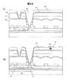
図30は、従来技術による半透過型の液晶表示装置の1画素付近の構成例を説明する断面図である。また、図31は、図30に示した1画素付近の構成例を説明する平面図である。この半透過型の液晶表示装置は、薄膜トランジスタ(TFT)を形成した一方の基板(第1の基板、以下、TFT基板とも言う)100とカラーフィルタを形成した基板(第2の基板、以下、対向基板とも言う)200との間に液晶300を封入して構成される。TFT基板100の背面にはバックライトが設置されるが、図示は省略した。
FIG. 30 is a cross-sectional view illustrating a configuration example near one pixel of a transflective liquid crystal display device according to the related art. FIG. 31 is a plan view for explaining a configuration example near one pixel shown in FIG. The transflective liquid crystal display device, thin film transistors while the substrate formed with (TFT) (first substrate, hereinafter referred to as TFT substrate) substrate formed with 100 and the color filter (a second substrate, below, opposite substrate also called) constituted by sealing
TFT基板100は、ガラス等の透明絶縁基板101の内面にTFT102で駆動される透明画素電極108と反射画素電極105を有する。反射画素電極105は透明画素電極108の上に形成されている。透明画素電極108はバックライトからの透過光LTを透過し、反射画素電極105は外光LRを反射する。反射画素電極105の下部には、TFT102のゲート電極124と同じ層からなる容量金属膜124Aと、TFT102のチャネルと同じ層からなるp−Si膜114の間にゲート絶縁膜125を介して保持容量109が形成されている。反射画素電極105には凹凸が形成されており、外光LRを散乱して対向基板200方向に反射する。この構成では、バックライトからの光は、反射電極の下部に形成された保持容量によって遮光されるため、光透過率が低下する。
The
ゲート電極124と容量金属膜124Aは層間絶縁膜118で覆われ、この層間絶縁膜118とゲート絶縁膜125を通してソース・ドレイン電極が形成され、その一方に配線122(=信号配線)が、他方には有機パス膜106Aを通して画素電極(透明画素電極108と反射画素電極105)が接続している。画素電極を構成する透明画素電極108と反射画素電極105を覆って、配向膜110が形成されている。
The
対向基板200は、ガラス等の透明絶縁基板201の内面にカラーフィルタ202、保護膜203、配向膜204がこの準で形成されている。なお、隣接するカラーフィルタとの間に遮光膜(ブラックマトリクス)を形成するのが一般的であるが、ここでは図示していない。反射画素電極105の領域に対応する部分の保護膜203は、外光LRと透過光LTに対するΔn・dを同じにするために液晶300の厚み(d)を1/2とする如く液晶300内に膨出している。
In the
1画素は、隣接する2本のゲート線126と2本の信号配線127で囲まれた領域に形成される。この領域の一部にTFT102を有し、TFT102で駆動される透明画素電極108と反射画素電極105で構成される画素電極が配置される。反射画素電極105の部分には保持容量109が形成されている。この保持容量109の一方の電極はストレージ線127に接続している。なお、図31には有機パス膜106Aの表面に有する凹凸128が示されている。
One pixel is formed in a region surrounded by two
図32は、図30と図31で説明した1画素の等価回路図である。図30および図31と同じ符号は同じ部分に対応し、繰り返しの説明はしない。 FIG. 32 is an equivalent circuit diagram of one pixel described in FIGS. 30 and 31 correspond to the same parts, and will not be described repeatedly.
図33は、図30〜図32で説明した従来技術による半透過液晶表示装置における反射レンズ構造を説明する模式図である。TFT基板100の内面における画素電極内に透明な絶縁材で形成した複数の突起ブロック151を有し、その上に第一の反射膜149が形成されている。第一の反射膜149は突起ブロック151の中央に開口を有しており、その下部に第二の反射膜150が形成されている。第一の反射膜149の下部で反射された光は、第二の反射膜150で反射され、第一の反射膜149の開口部を透過して対向基板200方向に出射する。この構成では、液晶駆動の面から光利用効率を高めるための画素電極構成、保持容量の構成、液晶の表示モードについては考慮されていない。
FIG. 33 is a schematic diagram for explaining a reflection lens structure in the transflective liquid crystal display device according to the prior art described with reference to FIGS. The pixel electrode on the inner surface of the
バックライトからの光を画素突起上に形成した反射層の裏面と、第二反射膜により集光して透過させ、実質的な光透過率を向上した反射レンズ構造を備えた半透過型の液晶表示装置を開示したものとしては、特許文献1を挙げることができる。また、反射電極下部に保持容量を設けた半透過型液晶表示装置に関しては特許文献2を、透明保持容量を用いた半透過型の横電界方式の液晶表示装置関しては特許文献3を挙げることができる。
前記した従来技術の反射レンズ構造では、(1)TFT基板への実装方法について考慮されていない、(2)反射レンズの電極形状が液晶駆動と整合しない、(3)反射電極の下部に保持容量を設けても透過率が低下する、(4)反射部と透過部が隣接するため、透過と反射の液晶厚みを変えて特性を合わせることが困難である等、の課題がある。 In the above-described conventional reflective lens structure, (1) the mounting method on the TFT substrate is not considered, (2) the electrode shape of the reflective lens does not match the liquid crystal drive, and (3) the storage capacitor below the reflective electrode. However, there is a problem that the transmittance is lowered even if the reflective layer is provided. (4) Since the reflective portion and the transmissive portion are adjacent to each other, it is difficult to match the characteristics by changing the thickness of the liquid crystal for transmission and reflection.
本発明の目的は、上記従来技術の課題を解決し、バックライトの消費電力低減と高画質の半透過型の液晶表示装置を提供することにある。 An object of the present invention is to solve the above-described problems of the prior art and provide a transflective liquid crystal display device with reduced backlight power consumption and high image quality.
本発明の液晶表示装置は、薄膜トランジスタを形成した一方の基板(TFT基板)と、カラーフィルタを形成した他方の基板(対向基板)と、前記一方の基板と前記他方の基板との貼り合わせ間隙に液晶を封入して構成される。 In the liquid crystal display device of the present invention, one substrate (TFT substrate) on which a thin film transistor is formed, the other substrate (counter substrate) on which a color filter is formed, and a bonding gap between the one substrate and the other substrate. Constructed by enclosing liquid crystal.
そして、上記目的を達成するため、本発明は、前記一方の基板の内面に設置されて、表裏両面に反射面をもつと共に前記対向基板側に凸形となる反射レンズ構造を有して該凸形の頂部に開口部を有する第一の反射電極と、
前記第一の反射電極と前記一方の基板の間、かつ前記第一の反射電極の前記開口部の下部に、前記第一の反射電極側の表面に反射面をもつ第二の反射膜とを備え、
前記一方の基板側から入射する光を前記第一の反射電極の裏面と第二の反射膜の表面で反射させ、前記第一の反射電極の前記開口部に集光して、前記他方の基板側に透過させることを特徴とする。
In order to achieve the above object, the present invention has a reflective lens structure that is provided on the inner surface of the one substrate, has reflection surfaces on both front and back surfaces, and has a convex shape on the counter substrate side. A first reflective electrode having an opening at the top of the shape;
A second reflective film having a reflective surface on the surface on the first reflective electrode side, between the first reflective electrode and the one substrate, and below the opening of the first reflective electrode; Prepared,
The light incident from the one substrate side is reflected by the back surface of the first reflective electrode and the surface of the second reflective film, and condensed on the opening of the first reflective electrode, and the other substrate It is characterized by transmitting to the side.
本発明では、前記凸形となる反射レンズ構造を構成する前記第一の反射電極を、前記第一の基板に形成した有機PAS膜の上層に有し、かつ当該有機PAS膜の表面の凹凸に倣った形状とすることができ、前記凸形となる反射レンズ構造を構成する前記第一の反射電極は前記第一の基板に形成した有機PAS膜の上層に有し、かつ当該有機PAS膜の表面の凹凸に倣った形状であり、前記第二の反射膜は前記有機PAS膜の下層に有することができる。 In the present invention, the first reflective electrode constituting the convex reflecting lens structure is provided on an upper layer of the organic PAS film formed on the first substrate, and the surface of the organic PAS film is uneven. The first reflecting electrode constituting the convex reflecting lens structure can be formed in a shape that follows the upper surface of the organic PAS film formed on the first substrate, and the organic PAS film The second reflection film can be formed in a lower layer of the organic PAS film.
また、本発明は、当該第一の反射電極の上層に絶縁膜を介して前記液晶駆動用の他方の電極を設け、前記第一の反射電極と前記他方の電極、および当該第一の反射電極および当該他方の電極の間に有する絶縁膜とで、保持容量を形成することができる。 In the present invention, the other electrode for driving the liquid crystal is provided on an upper layer of the first reflective electrode via an insulating film, the first reflective electrode, the other electrode, and the first reflective electrode. A storage capacitor can be formed using the insulating film between the other electrode.
また、本発明は、前記一方の基板の内面に設置されて、表裏両面に反射面をもつと共に前記対向基板側に凸形となる反射レンズ構造を有して該凸形の頂部に開口部を有する第一の反射電極と、
前記第一の反射電極と前記一方の基板の間、かつ前記第一の反射電極の前記開口部の下部に、前記第一の反射電極側の表面に反射面をもつ第二の反射膜と、
前記第一の反射電極の上層に絶縁膜を介して前記液晶駆動用の透明画素電極と、当該透明電極の上に、前記第一の反射電極の前記開口部を避けて形成された反射電極とを備え、
前記一方の基板側から入射する光を前記第一の反射電極の裏面と第二の反射膜の表面で反射させ、前記第一の反射電極の前記開口部に集光して、前記透明画素電極を通して前記他方の基板側に透過させる構成とすることができる。
Further, the present invention has a reflective lens structure that is installed on the inner surface of the one substrate, has reflection surfaces on both front and back surfaces, and is convex on the opposite substrate side, and has an opening at the top of the convex shape A first reflective electrode having
A second reflective film having a reflective surface on a surface on the first reflective electrode side between the first reflective electrode and the one substrate, and below the opening of the first reflective electrode;
A transparent pixel electrode for driving the liquid crystal through an insulating film on an upper layer of the first reflective electrode; a reflective electrode formed on the transparent electrode so as to avoid the opening of the first reflective electrode; With
The light incident from the one substrate side is reflected by the back surface of the first reflective electrode and the surface of the second reflective film, and condensed on the opening of the first reflective electrode, and the transparent pixel electrode It can be set as the structure which permeate | transmits to the said other board | substrate side.
また、本発明は、前記凸形となる反射レンズ構造を構成する前記第一の反射電極は、前記第一の基板に形成した有機PAS膜の上層に有し、かつ当該有機PAS膜の表面の凹凸に倣った形状とすると共に、前記透明画素電極は、前記第一の反射電極の上層に当該第一の反射電極の表面の凹凸に倣った形状の表面形状を有する絶縁膜の上に同様の凹凸形状で形成することができる。 Further, in the present invention, the first reflective electrode constituting the convex reflective lens structure has an upper layer of the organic PAS film formed on the first substrate, and is formed on the surface of the organic PAS film. The transparent pixel electrode has the same shape on the insulating film having a surface shape that follows the unevenness on the surface of the first reflective electrode. It can be formed in an uneven shape.
また、本発明は、前記第一の反射電極と前記透明画素電極、および当該第一の反射電極および当該透明画素電極の間に有する絶縁膜とで、保持容量を形成することができる。 In the present invention, a storage capacitor can be formed by the first reflective electrode, the transparent pixel electrode, and the insulating film between the first reflective electrode and the transparent pixel electrode.
また、本発明は、前記一方の基板の内面に設置されて、表裏両面に反射面をもつと共に前記対向基板側に凸形となる反射レンズ構造を有して該凸形の頂部に開口部を有する第一の反射電極と、
前記第一の反射電極と前記一方の基板の間、かつ前記第一の反射電極の前記開口部の下部に、前記第一の反射電極側の表面に反射面をもつ第二の反射膜と、
前記第一の反射電極との上層に、有機PAS膜を介して形成された位相差膜と、
前記位相差膜の上に形成された透明共通電極と、
前記透明共通電極の上層に、絶縁膜を介して形成された開口部をもつ透明画素電極とを有し、
前記一方の基板側から入射する光を前記第一の反射電極の裏面と第二の反射膜の表面で反射させ、前記第一の反射電極の前記開口部に集光して、前記他方の基板側に透過させることを特徴とする。
Further, the present invention has a reflective lens structure that is installed on the inner surface of the one substrate, has reflection surfaces on both front and back surfaces, and has a convex shape on the counter substrate side, and has an opening at the top of the convex shape. A first reflective electrode having
A second reflective film having a reflective surface on a surface on the first reflective electrode side between the first reflective electrode and the one substrate, and below the opening of the first reflective electrode;
A retardation film formed on the first reflective electrode via an organic PAS film,
A transparent common electrode formed on the retardation film;
A transparent pixel electrode having an opening formed through an insulating film on an upper layer of the transparent common electrode;
The light incident from the one substrate side is reflected by the back surface of the first reflective electrode and the surface of the second reflective film, and condensed on the opening of the first reflective electrode, and the other substrate It is characterized by transmitting to the side.
また、本発明は、前記透明共通電極と前記透明画素電極、および当該透明共通電極および当該透明画素電極の間に有する絶縁膜とで、保持容量を形成することができる。そして、また本発明は、前記他方の基板の内面にカラーフィルタと保護膜を設け、前記透明画素電極の開口部に対応する絶縁保護膜に凹部を形成することができる。 In the present invention, a storage capacitor can be formed by the transparent common electrode, the transparent pixel electrode, and the insulating film between the transparent common electrode and the transparent pixel electrode. In the present invention, a color filter and a protective film may be provided on the inner surface of the other substrate, and a recess may be formed in the insulating protective film corresponding to the opening of the transparent pixel electrode.
なお、本発明は、上記の構成および後述する実施の形態で説明される構成に限定されるものではなく、本発明の技術思想を逸脱することなく、種々の変更が可能である。 The present invention is not limited to the above-described configuration and the configuration described in the embodiments described later, and various modifications can be made without departing from the technical idea of the present invention.
本発明によれば、(1)現行のTFTプロセスで反射レンズ構成が得られ、光利用効率が向上する、(2)反射膜と別に透明電極を設けることにより、液晶駆動に必要な電極形状と反射レンズに必要な形状をそれぞれ最適化でき、光利用効率が向上する、(3)保持容量による光損失が抑制され、光透過率が向上する、(4)透過部と反射部が隣接していてもそれぞれ液晶の駆動を最適化できるため、画質の低下が抑制され、バックライトの消費電力が低減され、透過率を確保しつつ反射率を向上できることで、高画質の半透過型の液晶表示装置を提供できる。 According to the present invention, (1) a reflection lens configuration can be obtained by the current TFT process, and the light utilization efficiency is improved. (2) By providing a transparent electrode separately from the reflection film, the electrode shape necessary for driving the liquid crystal can be obtained. Each shape required for the reflective lens can be optimized to improve the light utilization efficiency. (3) Light loss due to the storage capacitor is suppressed and the light transmittance is improved. (4) The transmission part and the reflection part are adjacent to each other. However, since the drive of each liquid crystal can be optimized, the deterioration of image quality is suppressed, the power consumption of the backlight is reduced, and the reflectance can be improved while ensuring the transmittance, so that a high-quality transflective liquid crystal display Equipment can be provided.
以下、本発明の最良の形態を実施例の図面を参照して詳細に説明する。 The best mode of the present invention will be described below in detail with reference to the drawings of the embodiments.
図1は、本発明による半透過型液晶表示装置の実施例1を説明する断面図である。実施例1は、横電界型の半透過型液晶表示装置に本発明を適用したものである。図1において、TFT基板100と対向基板200の間に液晶300が封入されている。TFT基板100は、ガラス板を好適とする透明絶縁基板101の内面に図30と同様に薄膜トランジスタ(TFT)102が形成されている。対向基板200も同じくガラス板を好適とする透明絶縁基板201の内面に、カラーフィルタ202、保護膜203、配向膜204が形成されている。TFT基板100の最上層(液晶300との界面)にも配向膜110が形成されている。
FIG. 1 is a sectional view for explaining a first embodiment of a transflective liquid crystal display device according to the present invention. In Example 1, the present invention is applied to a horizontal electric field type transflective liquid crystal display device. In FIG. 1, a
TFT基板100の背面には、バックライト400が設置されている。バックライト400は、導光板401と光源(LED等)402、およびプリズムシート403等で構成される。プリズムシート403等には拡散シートなども含まれる。これは、図30に示した液晶表示装置でも同様である。TFT基板100の外面には偏光板111と位相差板112が、対向基板200の外面には偏光板205と位相差板206が、それぞれ設けられている。図30には、これらの偏光板と位相差板は図示が省略されている。
A
TFT基板100に第一の反射膜となる反射共通電極105を形成し、その上部に有機PAS膜からなる絶縁膜107を介して透明導電膜からなる透明画素電極108を形成する。反射共通電極105と透明画素電極108の間に、液晶300に印加する電圧を保持する保持容量109が形成される。また、反射共通電極105は表裏が反射面となっており、表裏の反射面は有機PAS膜の凹凸に倣った凹凸を有し、この形状で反射レンズを構成している。反射共通電極105には、その凸部の頂部に開口部153を有し、この開口部153の下部にAlを好適とする金属膜からなる信号配線103と同層の第二の反射膜となる配線層反射膜104を形成する。
A reflective
第一の反射膜である反射共通電極105には、上記の凹凸が対向基板200の外面から入射する外光を散乱して反射する。バックライト400から TFT基板100を通して入射する光は、反射共通電極105の裏面で反射され、さらに第二の反射膜である配線層反射膜104で反射され、反射共通電極105の開口部153に集光されて対向基板200側に透過する。なお、TFT102の上層には有機PAS膜106が形成されている。
The projections and depressions scatter and reflect external light incident from the outer surface of the
図2は、実施例1における反射レンズの構成例を説明図である。反射膜の凹凸は、例えば以下のように形成される。図2(a)において、有機PAS膜106の配線層反射膜104の表面からの厚みを、頂点部分で4μm、凹部で3μmとし、凸部の頂点付近に形成される開口部153の直径は4μm、その下部の配線層反射膜104の直径は5μmとする。有機PASの凸部の曲率半径及び開口部の間隔は12μm程度とする。
FIG. 2 is an explanatory diagram of a configuration example of the reflecting lens in the first embodiment. The unevenness of the reflective film is formed as follows, for example. In FIG. 2A, the thickness of the
この例では、反射膜共通電極105の裏面の焦点距離は6μmであり、TFT基板100の下部から垂直に入射したバックライト光Lは、配線層反射膜104の表面と有機PAS膜106の凸部表面の中間の位置に集光され、開口部153を透過する。有機PAS106の厚みを有機PAS膜106の凸部の曲率半径の1/4から1/3程度とし、該凸部の直径を曲率半径程度とし、開口部153とその下部の第二反射膜である配線層反射膜104の大きさを曲率半径の1/3程度とすると、透過率を高くすることができる。
In this example, the focal length of the back surface of the reflective film
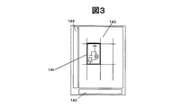
図3は、図1で説明した液晶表示装置を構成するTFT基板の模式図である。また、図4は、図3の画素部分の等価回路図である。基板101上にTFTで構成した画素146と、その駆動回路(ゲート線駆動回路144、信号線駆動回路145)を含む周辺回路が形成される。画素146には、ゲート線126の走査信号に応じて信号線127と画素電極108間のスイッチとなるTFTが形成されている。TFTがオンの状態で画素電極108に印加された電圧は、TFTをオフとした後も透明画素電極108と反射共通電極105間に形成された保持容量109により一定に保持され、液晶300に印加される。
FIG. 3 is a schematic diagram of a TFT substrate constituting the liquid crystal display device described in FIG. FIG. 4 is an equivalent circuit diagram of the pixel portion of FIG. A peripheral circuit including a
実施例1では、保持容量109は透明電極108と反射共通電極105の組み合わせからなり、配線層反射膜104の上部に形成され、バックライト400からの光及び外光を遮光することがないため、光の利用効率を高めることができる。これにより、バックライトの消費電力が低減され、透過率を確保しつつ反射率を向上できることで、高画質の半透過型の液晶表示装置を提供できる。
In the first embodiment, the
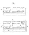
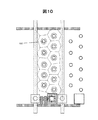
図5から図11は、図1に示した半透過型液晶表示装置の実施例1の製造工程の説明図であり、図5と図6は断面図、図7〜図11は図5と図6の要部平面図を示す。実施例1では、多結晶シリコン(Si)、所謂p−Siを用いたTFT基板を形成する例を説明する。先ず、ガラス基板101上にSiN、SiOの積層膜からなる下地絶縁膜(下地膜)113を介し、半導体層であるp−Si膜114を形成する(図5(a))。
5 to 11 are explanatory views of the manufacturing process of the transflective liquid crystal display device shown in FIG. 1 according to the first embodiment. FIGS. 5 and 6 are sectional views, and FIGS. 7 to 11 are FIGS. The principal part top view of 6 is shown. In Example 1, an example of forming a TFT substrate using polycrystalline silicon (Si), so-called p-Si will be described. First, a p-
SiOからなるゲート絶縁膜125、MoW合金からなるゲート124を順次形成する。この形成はCVDまたはスパッタを用いて膜を堆積した後、ホトリソグラフィー工程(ホト工程)で加工する。
A
ゲート加工後、Pイオンインプラによりソース116、ドレイン115および低濃度のドーパントが注入されたLDD123を形成する。この形成はゲート及びゲート加工時のレジストマスクをマスクとして、ゲートに対し自己整合的に行う(図5(b))。SiO膜からなる層間絶縁膜118を堆積後、コンタクトホール119を開口する(図5(c))、(図7)。MoW合金からなるバリア膜120、Al合金膜121を形成し、ホト工程により加工して信号配線122及び第二の反射膜となる配線層反射膜104を形成する(図5(d))、(図8)。
After the gate processing, the
有機PAS膜106を塗布し、ハーフトーンマスクにより部分的に露光し、現像、焼成をへて表面に凹凸128を形成する(図9)。有機PAS膜106上に、Al合金膜からなる反射共通電極105を形成して第一の反射膜とする(図6(a))、(図10)。反射共通電極上に、第二の有機PAS膜107を形成し、その上にITOからなる透明画素電極108を形成してTFT基板100を形成する。配線層反射膜104は、上層をAl合金として反射率を向上するが、透明画素電極108となるITOとAl合金を接触させた場合のコンタクト抵抗が高いという問題があるため、画素電極108は有機PAS膜107のスルーホール129及びコンタクトホール119を介して直接p−Si膜からなるTFTのソース電極116と接続する(図6(b))、(図11)。
An
実施例1では、透明画素電極108と反射共通電極間105に印加された電界により、液晶300を基板と平行な面内で回転させ、光の偏光状態を変調して偏光板111、205の透過率を変化させて画像を表示する。そして、反射部と透過部の特性を合わせるために、透過部では液晶の回転角を反射部より大とする。共通反射電極の開口部となる透過部の電極幅をその他の領域である反射部より小として電界を急峻化し、液晶の回転角を大としている。
In the first embodiment, the
図12は、本発明による半透過型液晶表示装置の実施例2を説明する断面図である。実施例2は、縦電界型の半透過型液晶表示装置に本発明を適用したものである。実施例2では、TFT基板100上に第一の反射膜となる反射共通電極105と、その上部にSiNからなる容量絶縁膜107Aを介して透明画素電極108と反射画素電極208を形成し、反射共通電極105との間に保持容量109を形成する。反射共通電極105及び反射画素電極208には開口部を形成し、その下部にAl配線と同層の第二の反射膜となる配線層反射膜104を形成する。
FIG. 12 is a sectional view for explaining a second embodiment of the transflective liquid crystal display device according to the present invention. In Example 2, the present invention is applied to a vertical electric field type transflective liquid crystal display device. In Example 2, the transparent
反射画素電極208には凹凸が形成され、外光LRを散乱して反射する。バックライト光LTは反射共通電極105の裏面で反射され、配線層反射膜104で反射されて反射共通電極105と反射画素電極208の開口部に集光されて透過する。
Irregularities are formed in the
実施例2では、保持容量109は透明画素電極108と反射共通電極105の組み合わせからなり、反射画素電極105の下部に形成され、バックライト光及び外光を遮光することがないため、光の利用効率を高めることができる。また、反射画素電極208と液晶300の間に配向膜110以外の膜がないことからも、反射率を高めることができる。
In the second embodiment, the
実施例2の液晶表示装置は、所謂垂直配向型(VA)である。この液晶表示装置は、電圧印加のない状態では液晶の分子は基板面に対して垂直方向に配向している。画素電極と対向基板上に形成された透明な対向電極との間に電界を印加することで液晶の分子の配向方向が傾斜し、液晶を透過する光の偏光状態を変調して表示する。液晶に電圧が印加されない状態では、透過及び反射のいずれも偏光板により遮光されるノーマリオフ状態となるよう、上下の偏光板と位相差板、及び液晶の配向が調整される。特に、液晶に入射する光が円偏光となるように配置すると、液晶層の厚みに対して黒表示が安定するため、コントラストを高くとることができる。 The liquid crystal display device of Example 2 is a so-called vertical alignment type (VA). In this liquid crystal display device, the molecules of the liquid crystal are aligned in the direction perpendicular to the substrate surface when no voltage is applied. By applying an electric field between the pixel electrode and the transparent counter electrode formed on the counter substrate, the alignment direction of the liquid crystal molecules is inclined, and the polarization state of the light transmitted through the liquid crystal is modulated and displayed. In a state where no voltage is applied to the liquid crystal, the alignment of the upper and lower polarizing plates, the phase difference plate, and the liquid crystal is adjusted so that both transmission and reflection are in a normally-off state where light is blocked by the polarizing plate. In particular, when the light incident on the liquid crystal is arranged so as to be circularly polarized, the black display is stable with respect to the thickness of the liquid crystal layer, so that the contrast can be increased.
透過部は透明電極を開口せず、反射電極のみを開口して対向電極との間の液晶に電界を印加する。透明画素電極及び反射画素電極が共に開口された部分では、液晶が傾斜しない点が形成され、また共通反射電極と画素電極間の電界により、その他の領域での液晶の傾斜を安定化させる。この点から透過部となる反射電極の開口部を画素電極の外周へ離すことで、透過部と反射部の特性のずれを調整する。他の構成は実施例1とほぼ同様である。 The transmissive part does not open the transparent electrode but opens only the reflective electrode and applies an electric field to the liquid crystal between the counter electrode. In a portion where both the transparent pixel electrode and the reflective pixel electrode are opened, a point where the liquid crystal does not tilt is formed, and the tilt of the liquid crystal in other regions is stabilized by the electric field between the common reflective electrode and the pixel electrode. From this point, the deviation of the characteristics of the transmissive part and the reflective part is adjusted by separating the opening of the reflective electrode serving as the transmissive part to the outer periphery of the pixel electrode. Other configurations are almost the same as those of the first embodiment.
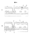
図13から図20は、図12の半透過型液晶表示装置の実施例2の製造工程の説明図であり、図13と図14は断面図、図15〜図20は図13と図14の要部平面図を示す。実施例2でも図5の例と同様に、TFT基板を形成する工程例である。先ず、p−Si膜114、ゲート絶縁膜125、ゲート124、ドレイン115、ソース116、SiO膜からなる層間絶縁膜118を堆積後、コンタクトホール119を開口する(図13(a)、図15)。
13 to 20 are explanatory views of the manufacturing process of the transflective liquid crystal display device of FIG. 12 according to the second embodiment. FIGS. 13 and 14 are sectional views, and FIGS. 15 to 20 are FIGS. The principal part top view is shown. Example 2 is a process example of forming a TFT substrate as in the example of FIG. First, after depositing an
Moからなるバリア膜120、Al合金膜121、Ag合金131を積層し、ホト工程により加工して配線122(信号配線127)及び第二の反射膜となる配線層反射膜104を形成する(図13(b)、図16)。
A
有機PAS膜106を塗布し、ハーフトーンマスクにより部分的に露光し、現像、焼成をへて表面に凹凸128を形成する(図17)。有機PAS上に、Ag合金膜とAl合金膜の積層膜からなる反射共通電極105を形成して第一の反射膜とする(図13(c)、図18)。
An
反射共通電極105上に、CVDを用いてSiNからなる容量絶縁膜107を形成し、ホト工程によりスルーホール129を開口する。その上にITOからなる透明画素電極108を形成する(図14(a)、図19)。その上に、反射画素電極208を形成し、TFT基板を得る。透明画素電極は、コンタクトホール119図13(a)、及びスルーホール129を介してTFTのソース116に接続される(図14(b)、図20)。
A capacitive insulating
第一の反射膜(反射共通電極105)は下層を、配線層反射膜104、反射画素電極208は上層をAg合金とし、反射率を向上させている。透明画素電極108となるITOとAl合金を接触させた場合のコンタクト抵抗が高いという問題があるため、反射画素電極208の下部にはMoからなるコンタクト層を積層する。反射共通電極105、配線層反射膜104及び反射画素電極208とも、ウェットエッチングを用いた一括加工をすることにより、工程を簡略化する。
The first reflective film (the reflective common electrode 105) has a lower layer, the wiring layer
図21は、本発明の実施例2における画素部分の等価回路図である。透明画素電極108に印加された電圧は、TFT102をオフとした後も透明画素電極108と反射共通電極105の間に容量絶縁膜107Aを介して形成された保持容量109により一定に保持され、液晶300に印加される。実施例2では、容量絶縁膜107Aに誘電率の大きいSiNを用いることで、保持容量109を大きくとることができ、画質が向上する。
FIG. 21 is an equivalent circuit diagram of a pixel portion according to the second embodiment of the present invention. The voltage applied to the
図22は、本発明による半透過型液晶表示装置の実施例3を説明する断面図である。実施例3は実施例1と異なる他の横電界型の液晶表示装置に本発明を適用したものである。図22において、第一の反射膜となる共通反射電極105と、第二の反射膜となる配線層反射膜104がTFT基板100上に形成されている。共通反射電極105上に、位相差膜138を介して透明共通電極137が形成されており、透明共通電極137上にSiNからなる容量絶縁膜107Aを介して透明画素電極108が形成されている。
FIG. 22 is a sectional view for explaining a third embodiment of the transflective liquid crystal display device according to the present invention. In the third embodiment, the present invention is applied to another lateral electric field type liquid crystal display device different from the first embodiment. In FIG. 22, a common
バックライト400からの光LTは、対向基板200の共通反射電極105と配線層反射膜104で反射され、共通反射電極105の開口部に集光され透過する。外光LRは、偏光板205及び位相差板206、カラーフィルタ(CF)202、液晶300、位相差膜138を通して共通反射電極105に入射し、散乱して対向基板200側に反射される。他の構成は実施例1を説明する図とほぼ同様である。
Light L T from the
実施例3では、保持容量109は第一の反射膜となる共通反射電極105上に、透明画素電極108と透明共通電極137の間に容量絶縁膜107Aを介して形成されており、外光およびバックライト光を遮光することはないため、光利用効率が向上する。
In the third embodiment, the
図23から図28は、図22に示した本発明の実施例3の半透過型液晶表示装置の製造工程を説明する図で、図23と図24は断面図、図25〜図28は図23と図24の要部平面図を示す。実施例3でも前記実施例と同様に、TFT基板を形成する工程例である。先ず、p−Si膜114、ゲート絶縁膜125、ゲート124、ドレイン115、ソース116、SiO膜からなる層間絶縁膜118を堆積後、コンタクトホールを開口する。Moからなるバリア膜120、Al合金膜121を積層し、ホト工程により加工して信号配線103及び第二の反射膜となる配線層反射膜104を形成する。
23 to 28 are diagrams for explaining the manufacturing process of the transflective liquid crystal display device according to the third embodiment of the present invention shown in FIG. 22, in which FIGS. 23 and 24 are sectional views, and FIGS. 23 and the principal part top view of FIG. 24 are shown. Example 3 is an example of a process for forming a TFT substrate as in the above example. First, a p-
有機PAS106を塗布し、ハーフトーンマスクにより部分的に露光し、現像、焼成をへて表面に凹凸を形成する。有機PAS106上に、Ag合金膜からなる反射共通電極105を形成して第一の反射膜とする。また、コンタクトホールで開口されたAl合金膜上にもAg合金膜を形成する(図23(a)、図25)。
An
反射共通電極105上に、平坦化膜107を塗布し、さらに位相差膜138を塗布した後、偏光紫外光を照射して位相差膜138及び有機PAS107を感光し、現像して未露光部を開口する。位相差膜138には偏光紫外光により異方性を生じる液晶やカイラル剤が添加されたUV硬化樹脂を含有し、平坦化膜107にはこれらを含まないUV硬化樹脂を用いることができる。
A flattening
平坦化膜107は、その上に形成される位相差膜138の膜厚を一定とし、位相差を均一化する。平坦化膜と位相差膜の一括露光により工程を簡略化できる。位相差膜138上に、透明共通電極137を形成する(図23(b)、図26)。透明共通電極137は位相差膜138及び平坦化膜107の開口部を介して反射共通電極105と接続される。(図24(a)、図27)
The
透明共通電極137の上にSiNからなる容量絶縁膜107Aを形成し、ホト工程によりスルーホール142を開口する。その上にITOからなる透明画素電極108を形成し、TFT基板100を得る。透明画素電極108は、コンタクトホール及びスルーホールを介してTFTのソース116に接続される(図24(b)、図28)。第一の反射膜である反射共通電極105は、ITOとのコンタクト性及び反射率に優れるAg合金とする。コンタクトホール内のAl合金膜上にもAg合金からなる第一の反射膜を積層し、ITOからなる画素電極108とのコンタクト性を改善する。
A capacitive insulating
実施例3では、透明画素電極108と透明共通電極137の間に印加された電界により、液晶の分子を基板面内で回転させ、光の偏光状態を変調して偏光板の透過率を変化させ、画像を表示する。反射部と透過部の特性を合わせるために、透過部では液晶の回転角を反射部より大とする。共通反射電極105の開口部となる透過部において、透明電極108の開口部の幅を小として電界を急峻化し、液晶の回転角を大としている。同様に、反射部と透過部の特性を合わせるため、透過部に対応する対向基板200の保護膜203には凹部203Aが設けられており、液晶300の層厚を反射部より大としている。保護膜203は平滑層としての機能も有する透明絶縁膜である。
In Example 3, an electric field applied between the
図29は、本発明の実施例3における画素部分の等価回路図である。画素電極に印加された電圧は、TFTをオフとした後も透明画素電極108と透明共通電極137間に容量絶縁膜107Aを介して形成された保持容量109により一定に保持され、液晶300に印加される。
FIG. 29 is an equivalent circuit diagram of a pixel portion according to the third embodiment of the present invention. The voltage applied to the pixel electrode is held constant by the
実施例3により、偏光板及び位相差膜、反射共通電極105上に形成された位相差膜は、液晶300に電圧が印加されていない状態で透過部及び反射部がともに黒表示となるように調整される。特に、液晶300に入射する光を直線偏光とし、また位相差膜を直線偏光が円偏光に変換される、いわゆる1/2波長板とすると、液晶300の層の厚みの変化に対する表示コントラストの低下が抑制される。位相差膜を形成する代わりに、反射共通電極105上に偏光吸収膜を形成してもよい。この場合、透過部と反射部の特性がより均一化される。
According to Example 3, the retardation film formed on the polarizing plate, the retardation film, and the reflective
上記した各実施例の何れにおいても、半導体膜としてp−Siの代わりにアモルファスSiからなる半導体膜や、ZnOなどの酸化物半導体膜、ペンタセンなどの有機半導体膜を用いたTFTを用いることもできる。また、透明電極にITOの代わりにZnO、SnOなど他の酸化物透明導電膜、透明有機導電膜、サブμm以下に細線化された金属配線を用いることもできる。 In any of the above embodiments, a TFT using a semiconductor film made of amorphous Si instead of p-Si, an oxide semiconductor film such as ZnO, and an organic semiconductor film such as pentacene can be used as the semiconductor film. . In addition, other oxide transparent conductive films such as ZnO and SnO, transparent organic conductive films, and metal wiring thinned to sub-μm or less can be used for the transparent electrode instead of ITO.
本発明の各実施例の液晶表示装置において、バックライトには、光源となるLEDと、光源からの光を均一に照射する導光板、導光板からの光の方向をほぼ垂直方向に変換するプリズムシートが含まれる。バックライト光をほぼ垂直方向から入射することで、第一及び第二の反射膜で反射された光の第一の反射膜の開口部への集光率が向上し、実効的な透過率が向上する。 In the liquid crystal display device of each embodiment of the present invention, the backlight includes an LED serving as a light source, a light guide plate that uniformly emits light from the light source, and a prism that converts the direction of light from the light guide plate into a substantially vertical direction. A sheet is included. By making the backlight light incident from substantially vertical direction, the light collection rate of the light reflected by the first and second reflection films to the opening of the first reflection film is improved, and the effective transmittance is increased. improves.
TFT基板との間に液晶をはさむ対向基板には、特定の色の光を透過するカラーフィルタが形成される。TFT基板及び対向基板の液晶と接する面には液晶の配向を制御するための配向膜が形成される。バックライトとTFT基板の間、及び対向基板の外部には、偏光状態を制御するための偏光板及び位相差板が設けられ、液晶を透過または反射した光の偏光状態により光を透過または吸収する機能を有する。本発明では、液晶に電圧が印加されていない状態では、透過及び反射のいずれも光が対向基板側の偏光板を透過しない、いわゆるノーマリオフ型となるよう配置されている。 A color filter that transmits light of a specific color is formed on the counter substrate sandwiching the liquid crystal between the TFT substrate. An alignment film for controlling the alignment of the liquid crystal is formed on the surface of the TFT substrate and the counter substrate that are in contact with the liquid crystal. A polarizing plate and a phase difference plate for controlling the polarization state are provided between the backlight and the TFT substrate and outside the counter substrate, and light is transmitted or absorbed depending on the polarization state of light transmitted or reflected by the liquid crystal. It has a function. In the present invention, in a state where no voltage is applied to the liquid crystal, both transmission and reflection are arranged so as to be a so-called normally-off type in which light does not pass through the polarizing plate on the counter substrate side.
100・・・薄膜トランジスタ基板(TFT基板)、101・・・ガラス基板、102・・・薄膜トランジスタ(TFT)、103・・・配線(信号配線)、104・・・配線層反射膜、105・・・反射共通電極、106, 106A, 107, 107A・・・絶縁膜、108・・・透明画素電極、109・・・保持容量、128・・・凹凸。
DESCRIPTION OF
Claims (21)
前記第1の基板の内面に設置されて、表裏両面に反射面をもつと共に前記第2の基板側に凸形となる反射レンズ構造を有して該凸形の頂部に開口部を有する第一の反射電極と、
前記第一の反射電極と前記第1の基板の間、かつ前記第一の反射電極の前記開口部の下部に、前記第一の反射電極側の表面に反射面をもつ第二の反射膜とを備え、
前記凸形となる反射レンズ構造を構成する前記第一の反射電極は、前記第1の基板に形成した有機PAS膜の上層に有し、かつ当該有機PAS膜の表面の凹凸に倣った形状であり、
前記第1の基板側から入射する光を前記第一の反射電極の裏面と第二の反射膜の表面で反射させ、前記第一の反射電極の前記開口部に集光して、前記第2の基板側に透過させることを特徴とする液晶表示装置。 A first substrate formed with thin film transistors, and a second substrate formed with a color filter, a liquid crystal display device constructed by filling liquid crystal in a lamination gap between the first substrate and the second substrate There,
A first lens is provided on the inner surface of the first substrate, has a reflecting surface on both front and back surfaces, and has a reflecting lens structure that is convex on the second substrate side, and has an opening at the top of the convex shape. A reflective electrode,
A second reflective film having a reflective surface on the surface on the first reflective electrode side, between the first reflective electrode and the first substrate and below the opening of the first reflective electrode; With
The first reflective electrode constituting the convex reflective lens structure has an upper layer of the organic PAS film formed on the first substrate and has a shape following the irregularities on the surface of the organic PAS film. Yes,
The light incident from the first substrate side is reflected by the back surface of the first reflective electrode and the surface of the second reflective film, and condensed on the opening of the first reflective electrode, and the second A liquid crystal display device characterized in that the liquid crystal display device is transmitted through the substrate side.
前記第二の反射膜は前記有機PAS膜の下層に有することを特徴とする液晶表示装置。 In claim 1,
The liquid crystal display device, wherein the second reflective film is provided below the organic PAS film.
前記第二の反射膜は、前記薄膜トランジスタの信号配線層と同層であることを特徴とする液晶表示装置。 In claim 2 ,
Before Symbol the second reflecting film, a liquid crystal display device which is a same layer as the signal wiring layers of the thin film transistor.
前記第一の反射電極の上層に絶縁膜を介して前記液晶駆動用の他方の電極を有することを特徴とする液晶表示装置。 In claim 1,
The liquid crystal display device characterized by having the other electrode for the liquid crystal driving through the upper layer insulating film before Symbol first reflective electrode.
前記第一の反射電極は共通電極であることを特徴とする液晶表示装置。 In claim 4 ,
The liquid crystal display device wherein the first reflective electrode, wherein the common electrode der Rukoto.
前記透明画素電極は前記薄膜トランジスタのソースまたはドレインに接続していることを特徴とする液晶表示装置。 In claim 5 ,
The liquid crystal display device, wherein the transparent pixel electrode is connected to a source or a drain of the thin film transistor.
前記第一の反射電極と前記透明画素電極、および当該第一の反射電極および当該他方の電極の間に有する絶縁膜とで、保持容量が形成されることを特徴とする液晶表示装置。 In claim 4 ,
A liquid crystal display device, wherein a storage capacitor is formed by the first reflective electrode, the transparent pixel electrode, and an insulating film between the first reflective electrode and the other electrode.
前記第1の基板の内面に設置されて、表裏両面に反射面をもつと共に前記第2の基板側に凸形となる反射レンズ構造を有して該凸形の頂部に開口部を有する第一の反射電極と、
前記第一の反射電極と前記第1の基板の間、かつ前記第一の反射電極の前記開口部の下部に、前記第一の反射電極側の表面に反射面をもつ第二の反射膜と、
前記第一の反射電極の上層に絶縁膜を介して前記液晶駆動用の透明画素電極と、当該透明電極の上層に、前記第一の反射電極の前記開口部を避けて形成された反射電極とを備え、
前記第1の基板側から入射する光を前記第一の反射電極の裏面と第二の反射膜の表面で反射させ、前記第一の反射電極の前記開口部に集光して、前記透明画素電極を通して前記第2の基板側に透過させることを特徴とする液晶表示装置。 A first substrate formed with thin film transistors, and a second substrate formed with a color filter, a liquid crystal display device constructed by filling liquid crystal in a lamination gap between the first substrate and the second substrate There,
A first lens is disposed on the inner surface of the first substrate, has a reflecting surface on both front and back surfaces, and has a reflecting lens structure that is convex on the second substrate side, and has an opening at the top of the convex shape. A reflective electrode,
A second reflective film having a reflective surface on the surface on the first reflective electrode side, between the first reflective electrode and the first substrate, and below the opening of the first reflective electrode; ,
Wherein the upper layer via an insulating film transparent pixel electrode for the liquid crystal driving of the first reflective electrode, the upper layer of the transparent electrode, the first the reflecting electrode formed to avoid the opening of the reflective electrode And
The light incident from the first substrate side is reflected by the back surface of the first reflective electrode and the surface of the second reflective film, and is collected at the opening of the first reflective electrode, and the transparent pixel A liquid crystal display device, wherein the liquid crystal display device transmits through the electrode to the second substrate side.
前記凸形となる反射レンズ構造を構成する前記第一の反射電極は、前記第1の基板に形成した有機PAS膜の上層に有し、かつ当該有機PAS膜の表面の凹凸に倣った形状であり、
前記透明画素電極は、前記第一の反射電極の上層に当該第一の反射電極の表面の凹凸に倣った形状の表面形状を有する絶縁膜の上に同様の凹凸形状で形成されていることを特徴とする液晶表示装置。 In claim 8 ,
The first reflective electrode constituting the convex reflective lens structure has an upper layer of the organic PAS film formed on the first substrate and has a shape following the irregularities on the surface of the organic PAS film. Yes,
The transparent pixel electrode is formed in a similar concavo-convex shape on an insulating film having a surface shape that follows the concavo-convex shape of the surface of the first reflective electrode on the first reflective electrode. A characteristic liquid crystal display device.
前記凸形となる反射レンズ構造を構成する前記第一の反射電極は前記第1の基板に形成した有機PAS膜の上層に有し、かつ当該有機PAS膜の表面の凹凸に倣った形状であり、
前記透明画素電極は、前記第一の反射電極の上層に当該第一の反射電極の表面の凹凸に倣った形状の表面形状を有する絶縁膜の上に同様の凹凸形状で形成され、
前記第二の反射膜は前記有機PAS膜の下層に有することを特徴とする液晶表示装置。 In claim 8 ,
The first reflective electrode constituting the convex reflective lens structure has an upper layer of the organic PAS film formed on the first substrate, and has a shape following the irregularities on the surface of the organic PAS film. ,
The transparent pixel electrode is formed in a similar concavo-convex shape on an insulating film having a surface shape that follows the concavo-convex shape of the surface of the first reflective electrode on the first reflective electrode.
The liquid crystal display device, wherein the second reflective film is provided below the organic PAS film.
前記第二の反射膜は、前記薄膜トランジスタの信号配線層と同層であることを特徴とする液晶表示装置。 In claim 10 ,
The liquid crystal display device, wherein the second reflective film is in the same layer as a signal wiring layer of the thin film transistor.
前記透明画素電極は前記液晶駆動用の電極であることを特徴とする液晶表示装置。 In claim 8 ,
The liquid crystal display device, wherein the transparent pixel electrode is an electrode for driving the liquid crystal.
前記透明画素電極は前記薄膜トランジスタのソースまたはドレインに接続していることを特徴とする液晶表示装置。 In claim 12 ,
The liquid crystal display device, wherein the transparent pixel electrode is connected to a source or a drain of the thin film transistor.
前記第一の反射電極と前記透明画素電極、および当該第一の反射電極および当該透明画素電極の間に有する絶縁膜とで、保持容量が形成されることを特徴とする液晶表示装置。 Oite to claim 9,
A storage capacitor is formed by the first reflective electrode, the transparent pixel electrode, and an insulating film between the first reflective electrode and the transparent pixel electrode.
前記第1の基板の内面に設置されて、表裏両面に反射面をもつと共に前記対向基板側に凸形となる反射レンズ構造を有して該凸形の頂部に開口部を有する第一の反射電極と、
前記第一の反射電極と前記第1の基板の間、かつ前記第一の反射電極の前記開口部の下部に、前記第一の反射電極側の表面に反射面をもつ第二の反射膜と、
前記第一の反射電極との上層に、有機PAS膜を介して形成された位相差膜と、
前記位相差膜の上に形成された透明共通電極と、
前記透明共通電極の上層に、絶縁膜を介して形成された開口部をもつ透明画素電極とを有し、
前記第1の基板側から入射する光を前記第一の反射電極の裏面と第二の反射膜の表面で反射させ、前記第一の反射電極の前記開口部に集光して、前記第2の基板側に透過させることを特徴とする液晶表示装置。 A first substrate formed with thin film transistors, and a second substrate formed with a color filter, a liquid crystal display device constructed by filling liquid crystal in a lamination gap between the first substrate and the second substrate There,
A first reflection which is installed on the inner surface of the first substrate, has a reflection surface on both front and back surfaces and has a convex lens structure on the opposite substrate side, and has an opening at the top of the convex shape. Electrodes,
A second reflective film having a reflective surface on the surface on the first reflective electrode side, between the first reflective electrode and the first substrate and below the opening of the first reflective electrode; ,
A retardation film formed on the first reflective electrode via an organic PAS film,
A transparent common electrode formed on the retardation film;
A transparent pixel electrode having an opening formed through an insulating film on an upper layer of the transparent common electrode;
The light incident from the first substrate side is reflected by the back surface of the first reflective electrode and the surface of the second reflective film, and condensed on the opening of the first reflective electrode, and the second A liquid crystal display device characterized in that the liquid crystal display device is transmitted through the substrate side.
前記凸形となる反射レンズ構造を構成する前記第一の反射電極は、前記第1の基板に形成した有機PAS膜の上層に有し、かつ当該有機PAS膜の表面の凹凸に倣った形状であることを特徴とする液晶表示装置。 In claim 15 ,
The first reflective electrode constituting the convex reflective lens structure has an upper layer of the organic PAS film formed on the first substrate and has a shape following the irregularities on the surface of the organic PAS film. There is a liquid crystal display device.
前記凸形となる反射レンズ構造を構成する前記第一の反射電極は前記第1の基板に形成した有機PAS膜の上層に有し、かつ当該有機PAS膜の表面の凹凸に倣った形状であり、前記第二の反射膜は前記有機PAS膜の下層に有することを特徴とする液晶表示装置。 In claim 15 ,
The first reflective electrode constituting the convex reflective lens structure has an upper layer of the organic PAS film formed on the first substrate, and has a shape following the irregularities on the surface of the organic PAS film. The liquid crystal display device, wherein the second reflective film is provided below the organic PAS film.
前記第二の反射膜は、前記薄膜トランジスタの信号配線層と同層であることを特徴とする液晶表示装置。 In claim 17 ,
The liquid crystal display device, wherein the second reflective film is the same layer as a signal wiring layer of the thin film transistor.
前記透明画素電極は前記薄膜トランジスタのソースまたはドレインに接続していることを特徴とする液晶表示装置。 In claim 17 ,
The liquid crystal display device, wherein the transparent pixel electrode is connected to a source or a drain of the thin film transistor.
前記透明共通電極と前記透明画素電極、および当該透明共通電極および当該透明画素電極の間に有する絶縁膜とで、保持容量が形成されることを特徴とする液晶表示装置。 In claim 15 ,
A storage capacitor is formed by the transparent common electrode, the transparent pixel electrode, and an insulating film between the transparent common electrode and the transparent pixel electrode.
前記第2の基板の内面にカラーフィルタと保護膜を有し、前記透明画素電極の開口部に対応する絶縁保護膜に凹部を有することを特徴とする液晶表示装置。 In claim 15 ,
A liquid crystal display device comprising: a color filter and a protective film on an inner surface of the second substrate; and a concave portion in an insulating protective film corresponding to the opening of the transparent pixel electrode.
Priority Applications (2)
| Application Number | Priority Date | Filing Date | Title |
|---|---|---|---|
| JP2006286007A JP4866703B2 (en) | 2006-10-20 | 2006-10-20 | Liquid crystal display |
| US11/907,058 US7643115B2 (en) | 2006-10-20 | 2007-10-09 | Liquid crystal display unit |
Applications Claiming Priority (1)
| Application Number | Priority Date | Filing Date | Title |
|---|---|---|---|
| JP2006286007A JP4866703B2 (en) | 2006-10-20 | 2006-10-20 | Liquid crystal display |
Publications (3)
| Publication Number | Publication Date |
|---|---|
| JP2008102397A JP2008102397A (en) | 2008-05-01 |
| JP2008102397A5 JP2008102397A5 (en) | 2009-08-20 |
| JP4866703B2 true JP4866703B2 (en) | 2012-02-01 |
Family
ID=39317553
Family Applications (1)
| Application Number | Title | Priority Date | Filing Date |
|---|---|---|---|
| JP2006286007A Expired - Fee Related JP4866703B2 (en) | 2006-10-20 | 2006-10-20 | Liquid crystal display |
Country Status (2)
| Country | Link |
|---|---|
| US (1) | US7643115B2 (en) |
| JP (1) | JP4866703B2 (en) |
Families Citing this family (25)
| Publication number | Priority date | Publication date | Assignee | Title |
|---|---|---|---|---|
| TW200921225A (en) * | 2007-11-06 | 2009-05-16 | Au Optronics Corp | Transflective liquid crystal display panel |
| JP5079462B2 (en) * | 2007-11-19 | 2012-11-21 | 株式会社ジャパンディスプレイウェスト | Liquid crystal device and electronic device |
| JP5408914B2 (en) * | 2008-07-03 | 2014-02-05 | 株式会社ジャパンディスプレイ | LCD panel |
| KR101560201B1 (en) * | 2008-08-27 | 2015-10-15 | 삼성디스플레이 주식회사 | Liquid crystal display panel and method of manufacturing the same |
| US8237643B2 (en) * | 2008-11-12 | 2012-08-07 | Himax Technologies Limited | Transreflective display apparatus and driving method thereof |
| US8654292B2 (en) * | 2009-05-29 | 2014-02-18 | Semiconductor Energy Laboratory Co., Ltd. | Liquid crystal display device and method for manufacturing the same |
| WO2011049230A1 (en) | 2009-10-21 | 2011-04-28 | Semiconductor Energy Laboratory Co., Ltd. | Voltage regulator circuit |
| KR101781788B1 (en) * | 2009-12-28 | 2017-09-26 | 가부시키가이샤 한도오따이 에네루기 켄큐쇼 | Liquid crystal display device and electronic device |
| WO2011081041A1 (en) * | 2009-12-28 | 2011-07-07 | Semiconductor Energy Laboratory Co., Ltd. | Semiconductor device and method for manufacturing the semiconductor device |
| CN102844806B (en) * | 2009-12-28 | 2016-01-20 | 株式会社半导体能源研究所 | Liquid crystal indicator and electronic equipment |
| KR101883331B1 (en) * | 2010-01-20 | 2018-08-30 | 가부시키가이샤 한도오따이 에네루기 켄큐쇼 | Display device and method for driving the same |
| WO2011089850A1 (en) * | 2010-01-20 | 2011-07-28 | Semiconductor Energy Laboratory Co., Ltd. | Method for driving liquid crystal display device |
| WO2011089853A1 (en) * | 2010-01-24 | 2011-07-28 | Semiconductor Energy Laboratory Co., Ltd. | Display device |
| US9000438B2 (en) * | 2010-02-26 | 2015-04-07 | Semiconductor Energy Laboratory Co., Ltd. | Semiconductor device and manufacturing method thereof |
| KR20120107721A (en) * | 2011-03-22 | 2012-10-04 | 삼성디스플레이 주식회사 | A fringe field switching mode liquid crystal display apparatus and an the manufacturing method thereof |
| CN103035734A (en) | 2011-10-07 | 2013-04-10 | 元太科技工业股份有限公司 | Metal oxide thin film transistor |
| US20140340607A1 (en) * | 2011-11-18 | 2014-11-20 | Sharp Kabushiki Kaisha | Semiconductor device, method for fabricating the semiconductor device and display device |
| CN103226270B (en) * | 2013-05-03 | 2016-01-20 | 合肥京东方光电科技有限公司 | A kind of semitransparent semi-inverse liquid crystal display panel, display device and array base palte |
| US9105615B1 (en) * | 2014-06-12 | 2015-08-11 | Amazon Technologies, Inc. | Substrate vias for a display device |
| KR102148491B1 (en) | 2015-12-14 | 2020-08-26 | 엘지디스플레이 주식회사 | Thin film transistor substrate |
| CN105867006B (en) * | 2016-03-10 | 2019-08-06 | 京东方科技集团股份有限公司 | Array substrate and its manufacturing method and display device |
| KR20180016271A (en) | 2016-08-05 | 2018-02-14 | 가부시키가이샤 한도오따이 에네루기 켄큐쇼 | Display device |
| TWI673550B (en) * | 2018-08-24 | 2019-10-01 | 友達光電股份有限公司 | Transflective display panel and pixel structure thereof |
| CN109212832B (en) * | 2018-10-30 | 2023-12-12 | 京东方科技集团股份有限公司 | Liquid crystal display panel, manufacturing method thereof and liquid crystal display device |
| JP2020079830A (en) * | 2018-11-12 | 2020-05-28 | 凸版印刷株式会社 | Thin-film transistor array and method for manufacturing the same |
Family Cites Families (11)
| Publication number | Priority date | Publication date | Assignee | Title |
|---|---|---|---|---|
| JP2955277B2 (en) | 1997-07-28 | 1999-10-04 | シャープ株式会社 | Liquid crystal display |
| JP4101454B2 (en) * | 2000-11-22 | 2008-06-18 | 株式会社日立製作所 | Liquid crystal display |
| TW510981B (en) * | 2001-12-31 | 2002-11-21 | Toppoly Optoelectronics Corp | Liquid crystal display panel |
| JP4117148B2 (en) * | 2002-05-24 | 2008-07-16 | 日本電気株式会社 | Transflective liquid crystal display device |
| JP4082683B2 (en) * | 2003-09-29 | 2008-04-30 | 株式会社 日立ディスプレイズ | Transflective liquid crystal display device |
| JP4223993B2 (en) * | 2004-05-25 | 2009-02-12 | 株式会社 日立ディスプレイズ | Liquid crystal display |
| JP4223992B2 (en) * | 2004-05-25 | 2009-02-12 | 株式会社 日立ディスプレイズ | Liquid crystal display |
| KR100648223B1 (en) * | 2005-05-11 | 2006-11-24 | 비오이 하이디스 테크놀로지 주식회사 | Transflective fringe field switching mode liquid crystal display |
| JP4380648B2 (en) * | 2005-05-25 | 2009-12-09 | エプソンイメージングデバイス株式会社 | Liquid crystal device and electronic device |
| EP1958019B1 (en) * | 2005-12-05 | 2017-04-12 | Semiconductor Energy Laboratory Co., Ltd. | Liquid crystal display device |
| KR101209044B1 (en) * | 2006-03-24 | 2012-12-06 | 삼성디스플레이 주식회사 | Liquid crystal display and method for manufacturing thereof |
-
2006
- 2006-10-20 JP JP2006286007A patent/JP4866703B2/en not_active Expired - Fee Related
-
2007
- 2007-10-09 US US11/907,058 patent/US7643115B2/en not_active Expired - Fee Related
Also Published As
| Publication number | Publication date |
|---|---|
| JP2008102397A (en) | 2008-05-01 |
| US7643115B2 (en) | 2010-01-05 |
| US20080094554A1 (en) | 2008-04-24 |
Similar Documents
| Publication | Publication Date | Title |
|---|---|---|
| JP4866703B2 (en) | Liquid crystal display | |
| JP5771365B2 (en) | Medium and small liquid crystal display | |
| KR102012854B1 (en) | Array substrate for liquid crystal display and method for fabricating the same | |
| KR101905757B1 (en) | Array substrate for fringe field switching mode liquid crystal display device and method for fabricating the same | |
| US7408597B2 (en) | Liquid crystal display device and method for fabricating the same | |
| US9711543B2 (en) | Liquid crystal display and method for manufacturing the same | |
| US9244320B2 (en) | Liquid crystal display and manufacturing method thereof | |
| JP5044098B2 (en) | Array substrate, manufacturing method thereof, and liquid crystal display device having the same | |
| KR102416573B1 (en) | Display device and manufacturing method thereof | |
| JP2011039478A (en) | Ffs mode liquid crystal display and method for manufacturing the same | |
| US7643114B2 (en) | Transflective display device with reflection pattern on the color filter substrate | |
| KR101282563B1 (en) | Liquid crystal display device and fabrication method of the same | |
| JP2008242428A (en) | Transflective liquid crystal display panel and method of fabricating the same | |
| US7995167B2 (en) | Liquid crystal display device and method for manufacturing liquid crystal display device | |
| KR20100059448A (en) | Thin film transistor array panel and manufacturing method thereof | |
| JP2016095336A (en) | Liquid crystal display device | |
| KR20080023904A (en) | Liquid crystal display and fabricating method thereof | |
| KR20070072299A (en) | Liquid crystal display device and the fabrication method | |
| JP6048075B2 (en) | Liquid crystal device and electronic device | |
| KR20110029921A (en) | Transflective type liquid crystal display device and methode of fabricating the same | |
| KR20110077254A (en) | Method of fabricating in plane switching mode liquid crystal display device | |
| JP2009122601A (en) | Method for manufacturing liquid crystal device | |
| KR100829708B1 (en) | Liquid crystal display and fabrication method thereof | |
| KR101071260B1 (en) | Transflective liquid crystal display | |
| JP2014164070A (en) | Color filter substrate, electro-optic device, method for manufacturing electro-optic device and electronic equipment |
Legal Events
| Date | Code | Title | Description |
|---|---|---|---|
| A521 | Written amendment |
Free format text: JAPANESE INTERMEDIATE CODE: A523 Effective date: 20090623 |
|
| A621 | Written request for application examination |
Free format text: JAPANESE INTERMEDIATE CODE: A621 Effective date: 20090623 |
|
| A711 | Notification of change in applicant |
Free format text: JAPANESE INTERMEDIATE CODE: A712 Effective date: 20110218 |
|
| RD03 | Notification of appointment of power of attorney |
Free format text: JAPANESE INTERMEDIATE CODE: A7423 Effective date: 20110218 |
|
| TRDD | Decision of grant or rejection written | ||
| A977 | Report on retrieval |
Free format text: JAPANESE INTERMEDIATE CODE: A971007 Effective date: 20111019 |
|
| A01 | Written decision to grant a patent or to grant a registration (utility model) |
Free format text: JAPANESE INTERMEDIATE CODE: A01 Effective date: 20111108 |
|
| A01 | Written decision to grant a patent or to grant a registration (utility model) |
Free format text: JAPANESE INTERMEDIATE CODE: A01 |
|
| A61 | First payment of annual fees (during grant procedure) |
Free format text: JAPANESE INTERMEDIATE CODE: A61 Effective date: 20111114 |
|
| FPAY | Renewal fee payment (event date is renewal date of database) |
Free format text: PAYMENT UNTIL: 20141118 Year of fee payment: 3 |
|
| R150 | Certificate of patent or registration of utility model |
Ref document number: 4866703 Country of ref document: JP Free format text: JAPANESE INTERMEDIATE CODE: R150 Free format text: JAPANESE INTERMEDIATE CODE: R150 |
|
| R250 | Receipt of annual fees |
Free format text: JAPANESE INTERMEDIATE CODE: R250 |
|
| R250 | Receipt of annual fees |
Free format text: JAPANESE INTERMEDIATE CODE: R250 |
|
| R250 | Receipt of annual fees |
Free format text: JAPANESE INTERMEDIATE CODE: R250 |
|
| R250 | Receipt of annual fees |
Free format text: JAPANESE INTERMEDIATE CODE: R250 |
|
| R250 | Receipt of annual fees |
Free format text: JAPANESE INTERMEDIATE CODE: R250 |
|
| R250 | Receipt of annual fees |
Free format text: JAPANESE INTERMEDIATE CODE: R250 |
|
| LAPS | Cancellation because of no payment of annual fees |