JP4863745B2 - 蛍光体粒子および波長変換器ならびに発光装置 - Google Patents
蛍光体粒子および波長変換器ならびに発光装置 Download PDFInfo
- Publication number
- JP4863745B2 JP4863745B2 JP2006085112A JP2006085112A JP4863745B2 JP 4863745 B2 JP4863745 B2 JP 4863745B2 JP 2006085112 A JP2006085112 A JP 2006085112A JP 2006085112 A JP2006085112 A JP 2006085112A JP 4863745 B2 JP4863745 B2 JP 4863745B2
- Authority
- JP
- Japan
- Prior art keywords
- light
- group
- particles
- wavelength
- liquid
- Prior art date
- Legal status (The legal status is an assumption and is not a legal conclusion. Google has not performed a legal analysis and makes no representation as to the accuracy of the status listed.)
- Expired - Fee Related
Links
Images


Classifications
-
- H—ELECTRICITY
- H01—ELECTRIC ELEMENTS
- H01L—SEMICONDUCTOR DEVICES NOT COVERED BY CLASS H10
- H01L2224/00—Indexing scheme for arrangements for connecting or disconnecting semiconductor or solid-state bodies and methods related thereto as covered by H01L24/00
- H01L2224/01—Means for bonding being attached to, or being formed on, the surface to be connected, e.g. chip-to-package, die-attach, "first-level" interconnects; Manufacturing methods related thereto
- H01L2224/26—Layer connectors, e.g. plate connectors, solder or adhesive layers; Manufacturing methods related thereto
- H01L2224/31—Structure, shape, material or disposition of the layer connectors after the connecting process
- H01L2224/32—Structure, shape, material or disposition of the layer connectors after the connecting process of an individual layer connector
- H01L2224/321—Disposition
- H01L2224/32151—Disposition the layer connector connecting between a semiconductor or solid-state body and an item not being a semiconductor or solid-state body, e.g. chip-to-substrate, chip-to-passive
- H01L2224/32221—Disposition the layer connector connecting between a semiconductor or solid-state body and an item not being a semiconductor or solid-state body, e.g. chip-to-substrate, chip-to-passive the body and the item being stacked
- H01L2224/32225—Disposition the layer connector connecting between a semiconductor or solid-state body and an item not being a semiconductor or solid-state body, e.g. chip-to-substrate, chip-to-passive the body and the item being stacked the item being non-metallic, e.g. insulating substrate with or without metallisation
-
- H—ELECTRICITY
- H01—ELECTRIC ELEMENTS
- H01L—SEMICONDUCTOR DEVICES NOT COVERED BY CLASS H10
- H01L2224/00—Indexing scheme for arrangements for connecting or disconnecting semiconductor or solid-state bodies and methods related thereto as covered by H01L24/00
- H01L2224/01—Means for bonding being attached to, or being formed on, the surface to be connected, e.g. chip-to-package, die-attach, "first-level" interconnects; Manufacturing methods related thereto
- H01L2224/42—Wire connectors; Manufacturing methods related thereto
- H01L2224/47—Structure, shape, material or disposition of the wire connectors after the connecting process
- H01L2224/48—Structure, shape, material or disposition of the wire connectors after the connecting process of an individual wire connector
- H01L2224/4805—Shape
- H01L2224/4809—Loop shape
- H01L2224/48091—Arched
-
- H—ELECTRICITY
- H01—ELECTRIC ELEMENTS
- H01L—SEMICONDUCTOR DEVICES NOT COVERED BY CLASS H10
- H01L2224/00—Indexing scheme for arrangements for connecting or disconnecting semiconductor or solid-state bodies and methods related thereto as covered by H01L24/00
- H01L2224/01—Means for bonding being attached to, or being formed on, the surface to be connected, e.g. chip-to-package, die-attach, "first-level" interconnects; Manufacturing methods related thereto
- H01L2224/42—Wire connectors; Manufacturing methods related thereto
- H01L2224/47—Structure, shape, material or disposition of the wire connectors after the connecting process
- H01L2224/48—Structure, shape, material or disposition of the wire connectors after the connecting process of an individual wire connector
- H01L2224/481—Disposition
- H01L2224/48151—Connecting between a semiconductor or solid-state body and an item not being a semiconductor or solid-state body, e.g. chip-to-substrate, chip-to-passive
- H01L2224/48221—Connecting between a semiconductor or solid-state body and an item not being a semiconductor or solid-state body, e.g. chip-to-substrate, chip-to-passive the body and the item being stacked
- H01L2224/48225—Connecting between a semiconductor or solid-state body and an item not being a semiconductor or solid-state body, e.g. chip-to-substrate, chip-to-passive the body and the item being stacked the item being non-metallic, e.g. insulating substrate with or without metallisation
- H01L2224/48227—Connecting between a semiconductor or solid-state body and an item not being a semiconductor or solid-state body, e.g. chip-to-substrate, chip-to-passive the body and the item being stacked the item being non-metallic, e.g. insulating substrate with or without metallisation connecting the wire to a bond pad of the item
-
- H—ELECTRICITY
- H01—ELECTRIC ELEMENTS
- H01L—SEMICONDUCTOR DEVICES NOT COVERED BY CLASS H10
- H01L2224/00—Indexing scheme for arrangements for connecting or disconnecting semiconductor or solid-state bodies and methods related thereto as covered by H01L24/00
- H01L2224/73—Means for bonding being of different types provided for in two or more of groups H01L2224/10, H01L2224/18, H01L2224/26, H01L2224/34, H01L2224/42, H01L2224/50, H01L2224/63, H01L2224/71
- H01L2224/732—Location after the connecting process
- H01L2224/73251—Location after the connecting process on different surfaces
- H01L2224/73265—Layer and wire connectors
Landscapes
- Luminescent Compositions (AREA)
- Led Device Packages (AREA)
- Led Devices (AREA)
Description
周期表第8族元素と周期表第16族元素との化合物、周期表第7族元素と周期表第16族元素との化合物、周期表第6族元素と周期表第16族元素との化合物、周期表第5族元素と周期表第16族元素との化合物、周期表第4族元素との周期表第16族元素との化合物、
周期表第2族元素と周期表第16族元素との化合物、カルコゲンスピネル類等が挙げられる。
周期表第13族元素と周期表第17族元素との化合物として、塩化タリウム(I)(TlCl)、臭化タリウム(I)(TlBr)、ヨウ化タリウム(I)(TlI)等、周期表第12族元素と周期表第16族元素との化合物として、酸化亜鉛(ZnO)、硫化亜鉛(ZnS)、セレン化亜鉛(ZnSe)、テルル化亜鉛(ZnTe)、酸化カドミウム(CdO)、硫化カドミウム(CdS)、セレン化カドミウム(CdSe)、テルル化カドミウム(CdTe)、硫化水銀(HgS)、セレン化水銀(HgSe)、テルル化水銀(HgTe)等、周期表第15族元素と周期表第16族元素との化合物として、硫化アンチモン(III)(Sb2S3)、セレン化アンチモン(III)(Sb2Se3)、テルル化アンチモン(III)(Sb2Te3)、硫化ビスマス(III)(Bi2S3)、セレン化ビスマス(III)(Bi2Se3)テルル化ビスマス(III)(Bi2Te3)等、周期表第11族元素と周期表第16族元素との化合物として、酸化銅(I)(Cu2O)等、周期表第11族元素と周期表第17族元素との化合物として、塩化銅(I)(CuCl)、臭化銅(I)(CuBr)、ヨウ化銅(I)(CuI)、ヨウ化銀(AgI)、塩化銀(AgCl)、臭化銀(AgBr)等、周期表第10族元素と周期表第16族元素との化合物として、酸化ニッケル(II)(NiO)等、周期表第9族元素との周期表第16族元素との化合物として、酸化コバルト(II)(CoO)、硫化コバルト(II)(CoS)等、周期表第8族元素と周期表第16族元素との化合物として、四酸化三鉄(Fe3O4)、硫化鉄(II)(FeS)等、周期表第7族元素と周期表第16族元素との化合物として、酸化マンガン(II)(MnO)等、周期表第6族元素と周期表第16族元素との化合物として、硫化モリブデン(IV)(MoS2)、酸化タングステン(IV)(WO2)等、周期表第5族元素と周期表第16族元素との化合物として、酸化バナジウム(II)(VO)、酸化バナジウム(II)(VO2)、酸化タンタル(V)(Ta2O5)等、周期表第4族元素との周期表第16族元素との化合物として、酸化チタン(TiO2、Ti2O5、Ti2O3、Ti5O9等)等、周期表第2族元素と周期表第16族元素との化合物として、硫化マグネシウム(MgS)、セレン化マグネシウム(MgSe)等、カルコゲンスピネル類として、酸化カドミウム(II)クロム(III)(CdCr2O4)、セレン化カドミウム(II)クロム(III)(CdCr2Se4)、硫化銅(II)クロム(III)(CuCr2S4)、セレン化水銀(II)クロム(III)(HgCr2Se4)等が挙げられる。
なお、測定して表に示した測定値はいずれも器を備えた波長変換器に関する値である。

3・・・中空粒状体
5・・・半導体超微粒子
7・・・液体
9・・・波長変換液
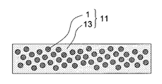
11・・・波長変換器
13・・・樹脂、マトリックス
15・・・発光素子
17・・・発光装置
Claims (9)
- 光を波長変換する半導体超微粒子と、液体とを含有してなるとともに含水率が0.1質量%以下であり、発光効率が40%以上の波長変換液が、透光性を有する平均粒径が0.05〜50μmの中空粒状体の中に封入されたことを特徴とする蛍光体粒子。
- 前記液体は、水の溶解度が0.1質量%以下であることを特徴とする請求項1記載の蛍光体粒子。
- 前記液体が変性シリコーンオイル、ジメチルシリコーンオイルの少なくとも1種からなることを特徴とする請求項1乃至2のうちいずれかに記載の蛍光体粒子。
- 前記液体がオレイルアミンまたはドデシルアミンの少なくとも1種からなることを特徴とする請求項1または2に記載の蛍光体粒子。
- 前記中空粒状体が前記半導体超微粒子から発せられた光を50%以上透過することを特徴とする請求項1乃至4のうちいずれかに記載の蛍光体粒子。
- 前記中空粒状体が、樹脂からなることを特徴とする請求項1乃至5のうちいずれかに記載の蛍光体粒子。
- 前記半導体超微粒子の平均粒子径が10nm以下であることを特徴とする請求項1乃至6のうちいずれかに記載の蛍光体粒子。
- 請求項1乃至7のうちいずれかに記載の蛍光体粒子を樹脂で固定してなることを特徴とする波長変換器。
- 発光素子と、該発光素子からの光を波長変換する請求項8に記載の波長変換器とを具備することを特徴とする発光装置。
Priority Applications (1)
| Application Number | Priority Date | Filing Date | Title |
|---|---|---|---|
| JP2006085112A JP4863745B2 (ja) | 2005-11-28 | 2006-03-27 | 蛍光体粒子および波長変換器ならびに発光装置 |
Applications Claiming Priority (3)
| Application Number | Priority Date | Filing Date | Title |
|---|---|---|---|
| JP2005342877 | 2005-11-28 | ||
| JP2005342877 | 2005-11-28 | ||
| JP2006085112A JP4863745B2 (ja) | 2005-11-28 | 2006-03-27 | 蛍光体粒子および波長変換器ならびに発光装置 |
Publications (2)
| Publication Number | Publication Date |
|---|---|
| JP2007173755A JP2007173755A (ja) | 2007-07-05 |
| JP4863745B2 true JP4863745B2 (ja) | 2012-01-25 |
Family
ID=38299872
Family Applications (1)
| Application Number | Title | Priority Date | Filing Date |
|---|---|---|---|
| JP2006085112A Expired - Fee Related JP4863745B2 (ja) | 2005-11-28 | 2006-03-27 | 蛍光体粒子および波長変換器ならびに発光装置 |
Country Status (1)
| Country | Link |
|---|---|
| JP (1) | JP4863745B2 (ja) |
Cited By (4)
| Publication number | Priority date | Publication date | Assignee | Title |
|---|---|---|---|---|
| US10964896B2 (en) | 2014-11-06 | 2021-03-30 | Postech Academy-Industry Foundation | Perovskite light-emitting device |
| US11205757B2 (en) | 2014-11-06 | 2021-12-21 | Sn Display Co., Ltd. | Core-shell structured perovskite particle light-emitter, method of preparing the same and light emitting device using the same |
| US11283035B2 (en) | 2014-11-06 | 2022-03-22 | Sn Display Co., Ltd. | Perovskite light emitting device containing exciton buffer layer and method for manufacturing same |
| US11588079B2 (en) | 2014-11-06 | 2023-02-21 | Postech Academy-Industry Foundation | Wavelength converting particle, method for manufacturing wavelength converting particle, and light-emitting diode containing wavelength converting particle |
Families Citing this family (8)
| Publication number | Priority date | Publication date | Assignee | Title |
|---|---|---|---|---|
| JP4960644B2 (ja) * | 2006-03-28 | 2012-06-27 | 京セラ株式会社 | 蛍光体粒子および波長変換器ならびに発光装置 |
| JP4960645B2 (ja) * | 2006-03-30 | 2012-06-27 | 京セラ株式会社 | 波長変換器および発光装置 |
| GB0821122D0 (en) | 2008-11-19 | 2008-12-24 | Nanoco Technologies Ltd | Semiconductor nanoparticle - based light emitting devices and associated materials and methods |
| GB0916699D0 (en) * | 2009-09-23 | 2009-11-04 | Nanoco Technologies Ltd | Semiconductor nanoparticle-based materials |
| GB0916700D0 (en) * | 2009-09-23 | 2009-11-04 | Nanoco Technologies Ltd | Semiconductor nanoparticle-based materials |
| JP5905648B2 (ja) * | 2013-07-08 | 2016-04-20 | Nsマテリアルズ株式会社 | 半導体を利用した発光デバイス |
| JP6401994B2 (ja) * | 2014-10-08 | 2018-10-10 | エルジー ディスプレイ カンパニー リミテッド | 液晶表示装置 |
| JP6651002B2 (ja) * | 2016-03-28 | 2020-02-19 | 富士フイルム株式会社 | 半導体量子ドットの製造方法及び半導体量子ドット |
Family Cites Families (9)
| Publication number | Priority date | Publication date | Assignee | Title |
|---|---|---|---|---|
| JP3412076B2 (ja) * | 1995-03-08 | 2003-06-03 | 株式会社リコー | 有機el素子 |
| JP4126751B2 (ja) * | 1998-05-26 | 2008-07-30 | ソニー株式会社 | 表示装置および照明装置 |
| JP2004107572A (ja) * | 2002-09-20 | 2004-04-08 | Sharp Corp | 蛍光体およびそれを含む照明装置と表示装置 |
| JP4653662B2 (ja) * | 2004-01-26 | 2011-03-16 | 京セラ株式会社 | 波長変換器、発光装置、波長変換器の製造方法および発光装置の製造方法 |
| JP4071724B2 (ja) * | 2004-02-09 | 2008-04-02 | 株式会社東芝 | Led照明装置 |
| JP4163641B2 (ja) * | 2004-02-25 | 2008-10-08 | 株式会社東芝 | Led素子 |
| JP4800669B2 (ja) * | 2005-06-07 | 2011-10-26 | セイコーインスツル株式会社 | 照明装置およびそれを用いた表示装置 |
| JP4771837B2 (ja) * | 2005-11-28 | 2011-09-14 | 京セラ株式会社 | 波長変換器および発光装置 |
| JP4960644B2 (ja) * | 2006-03-28 | 2012-06-27 | 京セラ株式会社 | 蛍光体粒子および波長変換器ならびに発光装置 |
-
2006
- 2006-03-27 JP JP2006085112A patent/JP4863745B2/ja not_active Expired - Fee Related
Cited By (6)
| Publication number | Priority date | Publication date | Assignee | Title |
|---|---|---|---|---|
| US10964896B2 (en) | 2014-11-06 | 2021-03-30 | Postech Academy-Industry Foundation | Perovskite light-emitting device |
| US11205757B2 (en) | 2014-11-06 | 2021-12-21 | Sn Display Co., Ltd. | Core-shell structured perovskite particle light-emitter, method of preparing the same and light emitting device using the same |
| US11283035B2 (en) | 2014-11-06 | 2022-03-22 | Sn Display Co., Ltd. | Perovskite light emitting device containing exciton buffer layer and method for manufacturing same |
| US11588079B2 (en) | 2014-11-06 | 2023-02-21 | Postech Academy-Industry Foundation | Wavelength converting particle, method for manufacturing wavelength converting particle, and light-emitting diode containing wavelength converting particle |
| US11730051B2 (en) | 2014-11-06 | 2023-08-15 | Sn Display Co., Ltd. | Perovskite light-emitting device |
| US11877460B2 (en) | 2014-11-06 | 2024-01-16 | Sn Display Co., Ltd. | Perovskite optoelectronic devices and method for manufacturing same |
Also Published As
| Publication number | Publication date |
|---|---|
| JP2007173755A (ja) | 2007-07-05 |
Similar Documents
| Publication | Publication Date | Title |
|---|---|---|
| JP4863745B2 (ja) | 蛍光体粒子および波長変換器ならびに発光装置 | |
| JP4771837B2 (ja) | 波長変換器および発光装置 | |
| JP4960644B2 (ja) | 蛍光体粒子および波長変換器ならびに発光装置 | |
| JP2007262375A (ja) | 波長変換器および発光装置 | |
| JP4653662B2 (ja) | 波長変換器、発光装置、波長変換器の製造方法および発光装置の製造方法 | |
| US7518160B2 (en) | Wavelength converter, lighting system, and lighting system assembly | |
| JP6631973B2 (ja) | 量子ドット複合材料ならびにその製造方法および用途 | |
| JP4969088B2 (ja) | 蛍光体及び波長変換器並びに発光装置 | |
| JP5907544B2 (ja) | ナノ粒子の製造方法 | |
| US10066164B2 (en) | Semiconductor nanocrystals used with LED sources | |
| JP2007146154A (ja) | 波長変換器、照明装置および照明装置集合体 | |
| JP2007157798A (ja) | 発光装置 | |
| JP4838005B2 (ja) | 発光装置 | |
| JP2007103512A (ja) | 発光装置 | |
| JP5371011B2 (ja) | 新規ナノ粒子発光体 | |
| US10879433B2 (en) | Stabilized quantum dot composite and method of making a stabilized quantum dot composite | |
| Chang et al. | Preparation of highly luminescent BaSO 4 protected CdTe quantum dots as conversion materials for excellent color-rendering white LEDs | |
| JP7226789B2 (ja) | 発光装置 | |
| JP7278371B2 (ja) | 量子ドット、波長変換材料、バックライトユニット、画像表示装置及び量子ドットの製造方法 | |
| JP2007197612A (ja) | 蛍光体及び波長変換器並びに発光装置 | |
| KR20180076386A (ko) | 고분자 코팅 양자점 및 이를 이용한 led 형광체 봉지제 제조 방법 | |
| Zhang et al. | Synthesis and enhanced photo/thermal stability of high-luminescent red-emitting CdTe@ CaCO3 composite for LED applications | |
| TW201605758A (zh) | 附著有螢光體之玻璃粉末及波長轉換構件之製造方法與波長轉換構件 | |
| JP7254824B2 (ja) | 硬化性シリコーン組成物及びその硬化物 | |
| TW556365B (en) | Method to fabricate LED for white light source |
Legal Events
| Date | Code | Title | Description |
|---|---|---|---|
| A621 | Written request for application examination |
Free format text: JAPANESE INTERMEDIATE CODE: A621 Effective date: 20080916 |
|
| A977 | Report on retrieval |
Free format text: JAPANESE INTERMEDIATE CODE: A971007 Effective date: 20111003 |
|
| TRDD | Decision of grant or rejection written | ||
| A01 | Written decision to grant a patent or to grant a registration (utility model) |
Free format text: JAPANESE INTERMEDIATE CODE: A01 Effective date: 20111011 |
|
| A01 | Written decision to grant a patent or to grant a registration (utility model) |
Free format text: JAPANESE INTERMEDIATE CODE: A01 |
|
| A61 | First payment of annual fees (during grant procedure) |
Free format text: JAPANESE INTERMEDIATE CODE: A61 Effective date: 20111108 |
|
| FPAY | Renewal fee payment (event date is renewal date of database) |
Free format text: PAYMENT UNTIL: 20141118 Year of fee payment: 3 |
|
| R150 | Certificate of patent or registration of utility model |
Free format text: JAPANESE INTERMEDIATE CODE: R150 |
|
| LAPS | Cancellation because of no payment of annual fees |