JP4852224B2 - Organic EL device manufacturing equipment - Google Patents
Organic EL device manufacturing equipment Download PDFInfo
- Publication number
- JP4852224B2 JP4852224B2 JP2003195296A JP2003195296A JP4852224B2 JP 4852224 B2 JP4852224 B2 JP 4852224B2 JP 2003195296 A JP2003195296 A JP 2003195296A JP 2003195296 A JP2003195296 A JP 2003195296A JP 4852224 B2 JP4852224 B2 JP 4852224B2
- Authority
- JP
- Japan
- Prior art keywords
- liquid material
- organic
- ink
- ion exchange
- container
- Prior art date
- Legal status (The legal status is an assumption and is not a legal conclusion. Google has not performed a legal analysis and makes no representation as to the accuracy of the status listed.)
- Expired - Fee Related
Links
- 238000004519 manufacturing process Methods 0.000 title claims description 40
- 239000000463 material Substances 0.000 claims description 100
- 239000011344 liquid material Substances 0.000 claims description 91
- 239000010410 layer Substances 0.000 claims description 72
- 238000001914 filtration Methods 0.000 claims description 50
- 238000005342 ion exchange Methods 0.000 claims description 44
- 239000012535 impurity Substances 0.000 claims description 43
- 239000002346 layers by function Substances 0.000 claims description 40
- 238000002347 injection Methods 0.000 claims description 34
- 239000007924 injection Substances 0.000 claims description 34
- 239000000758 substrate Substances 0.000 claims description 34
- 239000002612 dispersion medium Substances 0.000 claims description 21
- 229920001609 Poly(3,4-ethylenedioxythiophene) Polymers 0.000 claims description 17
- SECXISVLQFMRJM-UHFFFAOYSA-N N-Methylpyrrolidone Chemical compound CN1CCCC1=O SECXISVLQFMRJM-UHFFFAOYSA-N 0.000 claims description 14
- 238000003756 stirring Methods 0.000 claims description 12
- 238000007599 discharging Methods 0.000 claims description 8
- 229920000172 poly(styrenesulfonic acid) Polymers 0.000 claims description 7
- 229940005642 polystyrene sulfonic acid Drugs 0.000 claims description 7
- 239000002904 solvent Substances 0.000 claims description 7
- CYSGHNMQYZDMIA-UHFFFAOYSA-N 1,3-Dimethyl-2-imidazolidinon Chemical compound CN1CCN(C)C1=O CYSGHNMQYZDMIA-UHFFFAOYSA-N 0.000 claims description 6
- 239000000976 ink Substances 0.000 description 82
- 238000000034 method Methods 0.000 description 30
- 239000003456 ion exchange resin Substances 0.000 description 15
- 229920003303 ion-exchange polymer Polymers 0.000 description 15
- 239000003960 organic solvent Substances 0.000 description 15
- 229910001410 inorganic ion Inorganic materials 0.000 description 13
- NWUYHJFMYQTDRP-UHFFFAOYSA-N 1,2-bis(ethenyl)benzene;1-ethenyl-2-ethylbenzene;styrene Chemical group C=CC1=CC=CC=C1.CCC1=CC=CC=C1C=C.C=CC1=CC=CC=C1C=C NWUYHJFMYQTDRP-UHFFFAOYSA-N 0.000 description 10
- 150000001450 anions Chemical class 0.000 description 8
- LJCFOYOSGPHIOO-UHFFFAOYSA-N antimony pentoxide Chemical compound O=[Sb](=O)O[Sb](=O)=O LJCFOYOSGPHIOO-UHFFFAOYSA-N 0.000 description 8
- 150000001768 cations Chemical class 0.000 description 8
- 238000003860 storage Methods 0.000 description 8
- 238000004140 cleaning Methods 0.000 description 7
- 230000006866 deterioration Effects 0.000 description 7
- 238000010586 diagram Methods 0.000 description 7
- 230000005525 hole transport Effects 0.000 description 7
- QAOWNCQODCNURD-UHFFFAOYSA-L Sulfate Chemical compound [O-]S([O-])(=O)=O QAOWNCQODCNURD-UHFFFAOYSA-L 0.000 description 6
- 239000003957 anion exchange resin Substances 0.000 description 6
- 230000008859 change Effects 0.000 description 6
- 239000010408 film Substances 0.000 description 6
- 150000002500 ions Chemical class 0.000 description 6
- 229910052751 metal Inorganic materials 0.000 description 6
- 239000002184 metal Substances 0.000 description 6
- 238000007789 sealing Methods 0.000 description 6
- 239000004698 Polyethylene Substances 0.000 description 5
- 230000000694 effects Effects 0.000 description 5
- 238000002156 mixing Methods 0.000 description 5
- -1 polyethylene Polymers 0.000 description 5
- 229920000573 polyethylene Polymers 0.000 description 5
- 239000007787 solid Substances 0.000 description 5
- 239000000126 substance Substances 0.000 description 5
- PPBRXRYQALVLMV-UHFFFAOYSA-N Styrene Chemical compound C=CC1=CC=CC=C1 PPBRXRYQALVLMV-UHFFFAOYSA-N 0.000 description 4
- 230000015572 biosynthetic process Effects 0.000 description 4
- 125000000524 functional group Chemical group 0.000 description 4
- 239000007788 liquid Substances 0.000 description 4
- 239000002245 particle Substances 0.000 description 4
- 239000011347 resin Substances 0.000 description 4
- 229920005989 resin Polymers 0.000 description 4
- 229910001415 sodium ion Inorganic materials 0.000 description 4
- XUIMIQQOPSSXEZ-UHFFFAOYSA-N Silicon Chemical compound [Si] XUIMIQQOPSSXEZ-UHFFFAOYSA-N 0.000 description 3
- 229910052782 aluminium Inorganic materials 0.000 description 3
- 239000000919 ceramic Substances 0.000 description 3
- 239000000470 constituent Substances 0.000 description 3
- 230000002542 deteriorative effect Effects 0.000 description 3
- 239000006185 dispersion Substances 0.000 description 3
- 238000011049 filling Methods 0.000 description 3
- 230000010365 information processing Effects 0.000 description 3
- 229910021645 metal ion Inorganic materials 0.000 description 3
- 239000000203 mixture Substances 0.000 description 3
- 229920000642 polymer Polymers 0.000 description 3
- 229910052710 silicon Inorganic materials 0.000 description 3
- 239000010703 silicon Substances 0.000 description 3
- VYPSYNLAJGMNEJ-UHFFFAOYSA-N silicon dioxide Inorganic materials O=[Si]=O VYPSYNLAJGMNEJ-UHFFFAOYSA-N 0.000 description 3
- 239000002253 acid Substances 0.000 description 2
- NIXOWILDQLNWCW-UHFFFAOYSA-N acrylic acid group Chemical group C(C=C)(=O)O NIXOWILDQLNWCW-UHFFFAOYSA-N 0.000 description 2
- XAGFODPZIPBFFR-UHFFFAOYSA-N aluminium Chemical compound [Al] XAGFODPZIPBFFR-UHFFFAOYSA-N 0.000 description 2
- 229910000416 bismuth oxide Inorganic materials 0.000 description 2
- 239000003729 cation exchange resin Substances 0.000 description 2
- ZYGHJZDHTFUPRJ-UHFFFAOYSA-N coumarin Chemical compound C1=CC=C2OC(=O)C=CC2=C1 ZYGHJZDHTFUPRJ-UHFFFAOYSA-N 0.000 description 2
- 239000013078 crystal Substances 0.000 description 2
- TYIXMATWDRGMPF-UHFFFAOYSA-N dibismuth;oxygen(2-) Chemical compound [O-2].[O-2].[O-2].[Bi+3].[Bi+3] TYIXMATWDRGMPF-UHFFFAOYSA-N 0.000 description 2
- 238000001035 drying Methods 0.000 description 2
- 238000005401 electroluminescence Methods 0.000 description 2
- 239000011521 glass Substances 0.000 description 2
- 239000010931 gold Substances 0.000 description 2
- 239000011777 magnesium Substances 0.000 description 2
- 239000011159 matrix material Substances 0.000 description 2
- 238000005259 measurement Methods 0.000 description 2
- 239000004745 nonwoven fabric Substances 0.000 description 2
- RVTZCBVAJQQJTK-UHFFFAOYSA-N oxygen(2-);zirconium(4+) Chemical compound [O-2].[O-2].[Zr+4] RVTZCBVAJQQJTK-UHFFFAOYSA-N 0.000 description 2
- 230000008569 process Effects 0.000 description 2
- 239000002994 raw material Substances 0.000 description 2
- 239000004065 semiconductor Substances 0.000 description 2
- 239000011343 solid material Substances 0.000 description 2
- 239000010409 thin film Substances 0.000 description 2
- 239000002759 woven fabric Substances 0.000 description 2
- 229910001928 zirconium oxide Inorganic materials 0.000 description 2
- JCXLYAWYOTYWKM-UHFFFAOYSA-N (2,3,4-triphenylcyclopenta-1,3-dien-1-yl)benzene Chemical class C1C(C=2C=CC=CC=2)=C(C=2C=CC=CC=2)C(C=2C=CC=CC=2)=C1C1=CC=CC=C1 JCXLYAWYOTYWKM-UHFFFAOYSA-N 0.000 description 1
- QGKMIGUHVLGJBR-UHFFFAOYSA-M (4z)-1-(3-methylbutyl)-4-[[1-(3-methylbutyl)quinolin-1-ium-4-yl]methylidene]quinoline;iodide Chemical compound [I-].C12=CC=CC=C2N(CCC(C)C)C=CC1=CC1=CC=[N+](CCC(C)C)C2=CC=CC=C12 QGKMIGUHVLGJBR-UHFFFAOYSA-M 0.000 description 1
- AZQWKYJCGOJGHM-UHFFFAOYSA-N 1,4-benzoquinone Chemical compound O=C1C=CC(=O)C=C1 AZQWKYJCGOJGHM-UHFFFAOYSA-N 0.000 description 1
- VFBJMPNFKOMEEW-UHFFFAOYSA-N 2,3-diphenylbut-2-enedinitrile Chemical group C=1C=CC=CC=1C(C#N)=C(C#N)C1=CC=CC=C1 VFBJMPNFKOMEEW-UHFFFAOYSA-N 0.000 description 1
- DDTHMESPCBONDT-UHFFFAOYSA-N 4-(4-oxocyclohexa-2,5-dien-1-ylidene)cyclohexa-2,5-dien-1-one Chemical class C1=CC(=O)C=CC1=C1C=CC(=O)C=C1 DDTHMESPCBONDT-UHFFFAOYSA-N 0.000 description 1
- 239000005725 8-Hydroxyquinoline Substances 0.000 description 1
- GJCOSYZMQJWQCA-UHFFFAOYSA-N 9H-xanthene Chemical compound C1=CC=C2CC3=CC=CC=C3OC2=C1 GJCOSYZMQJWQCA-UHFFFAOYSA-N 0.000 description 1
- QTBSBXVTEAMEQO-UHFFFAOYSA-M Acetate Chemical compound CC([O-])=O QTBSBXVTEAMEQO-UHFFFAOYSA-M 0.000 description 1
- 229920003043 Cellulose fiber Polymers 0.000 description 1
- BDAGIHXWWSANSR-UHFFFAOYSA-M Formate Chemical compound [O-]C=O BDAGIHXWWSANSR-UHFFFAOYSA-M 0.000 description 1
- 239000005909 Kieselgur Substances 0.000 description 1
- FYYHWMGAXLPEAU-UHFFFAOYSA-N Magnesium Chemical compound [Mg] FYYHWMGAXLPEAU-UHFFFAOYSA-N 0.000 description 1
- 229930192627 Naphthoquinone Natural products 0.000 description 1
- MUBZPKHOEPUJKR-UHFFFAOYSA-L Oxalate Chemical compound [O-]C(=O)C([O-])=O MUBZPKHOEPUJKR-UHFFFAOYSA-L 0.000 description 1
- 229910052581 Si3N4 Inorganic materials 0.000 description 1
- BQCADISMDOOEFD-UHFFFAOYSA-N Silver Chemical compound [Ag] BQCADISMDOOEFD-UHFFFAOYSA-N 0.000 description 1
- CDBYLPFSWZWCQE-UHFFFAOYSA-L Sodium Carbonate Chemical compound [Na+].[Na+].[O-]C([O-])=O CDBYLPFSWZWCQE-UHFFFAOYSA-L 0.000 description 1
- PJANXHGTPQOBST-VAWYXSNFSA-N Stilbene Natural products C=1C=CC=CC=1/C=C/C1=CC=CC=C1 PJANXHGTPQOBST-VAWYXSNFSA-N 0.000 description 1
- GWEVSGVZZGPLCZ-UHFFFAOYSA-N Titan oxide Chemical compound O=[Ti]=O GWEVSGVZZGPLCZ-UHFFFAOYSA-N 0.000 description 1
- 230000004931 aggregating effect Effects 0.000 description 1
- PNEYBMLMFCGWSK-UHFFFAOYSA-N aluminium oxide Inorganic materials [O-2].[O-2].[O-2].[Al+3].[Al+3] PNEYBMLMFCGWSK-UHFFFAOYSA-N 0.000 description 1
- 150000001412 amines Chemical class 0.000 description 1
- 238000005349 anion exchange Methods 0.000 description 1
- 150000001454 anthracenes Chemical class 0.000 description 1
- PYKYMHQGRFAEBM-UHFFFAOYSA-N anthraquinone Natural products CCC(=O)c1c(O)c2C(=O)C3C(C=CC=C3O)C(=O)c2cc1CC(=O)OC PYKYMHQGRFAEBM-UHFFFAOYSA-N 0.000 description 1
- 150000004056 anthraquinones Chemical class 0.000 description 1
- 229910052787 antimony Inorganic materials 0.000 description 1
- WATWJIUSRGPENY-UHFFFAOYSA-N antimony atom Chemical compound [Sb] WATWJIUSRGPENY-UHFFFAOYSA-N 0.000 description 1
- 150000004982 aromatic amines Chemical class 0.000 description 1
- 230000004888 barrier function Effects 0.000 description 1
- 229910001423 beryllium ion Inorganic materials 0.000 description 1
- 229910052797 bismuth Inorganic materials 0.000 description 1
- JCXGWMGPZLAOME-UHFFFAOYSA-N bismuth atom Chemical compound [Bi] JCXGWMGPZLAOME-UHFFFAOYSA-N 0.000 description 1
- 238000009835 boiling Methods 0.000 description 1
- 230000015556 catabolic process Effects 0.000 description 1
- 238000005341 cation exchange Methods 0.000 description 1
- 229940023913 cation exchange resins Drugs 0.000 description 1
- 239000013522 chelant Substances 0.000 description 1
- 229920000547 conjugated polymer Polymers 0.000 description 1
- 229960000956 coumarin Drugs 0.000 description 1
- 235000001671 coumarin Nutrition 0.000 description 1
- 230000007423 decrease Effects 0.000 description 1
- 230000007547 defect Effects 0.000 description 1
- 238000006731 degradation reaction Methods 0.000 description 1
- 150000002009 diols Chemical class 0.000 description 1
- 239000000975 dye Substances 0.000 description 1
- 238000005530 etching Methods 0.000 description 1
- 238000001704 evaporation Methods 0.000 description 1
- 230000008020 evaporation Effects 0.000 description 1
- 238000002474 experimental method Methods 0.000 description 1
- 239000000835 fiber Substances 0.000 description 1
- 239000012530 fluid Substances 0.000 description 1
- 150000008376 fluorenones Chemical class 0.000 description 1
- PCHJSUWPFVWCPO-UHFFFAOYSA-N gold Chemical compound [Au] PCHJSUWPFVWCPO-UHFFFAOYSA-N 0.000 description 1
- 229910052737 gold Inorganic materials 0.000 description 1
- 238000010438 heat treatment Methods 0.000 description 1
- 229910001385 heavy metal Inorganic materials 0.000 description 1
- 150000007857 hydrazones Chemical class 0.000 description 1
- YAMHXTCMCPHKLN-UHFFFAOYSA-N imidazolidin-2-one Chemical compound O=C1NCCN1 YAMHXTCMCPHKLN-UHFFFAOYSA-N 0.000 description 1
- AMGQUBHHOARCQH-UHFFFAOYSA-N indium;oxotin Chemical compound [In].[Sn]=O AMGQUBHHOARCQH-UHFFFAOYSA-N 0.000 description 1
- 229910010272 inorganic material Inorganic materials 0.000 description 1
- 239000011147 inorganic material Substances 0.000 description 1
- RVSFRSNANSEBKV-UHFFFAOYSA-J lead(2+);hydroxide;phosphate Chemical compound [OH-].[Pb+2].[Pb+2].[O-]P([O-])([O-])=O RVSFRSNANSEBKV-UHFFFAOYSA-J 0.000 description 1
- QDLAGTHXVHQKRE-UHFFFAOYSA-N lichenxanthone Natural products COC1=CC(O)=C2C(=O)C3=C(C)C=C(OC)C=C3OC2=C1 QDLAGTHXVHQKRE-UHFFFAOYSA-N 0.000 description 1
- 239000004973 liquid crystal related substance Substances 0.000 description 1
- 238000011068 loading method Methods 0.000 description 1
- 229910052749 magnesium Inorganic materials 0.000 description 1
- 239000002609 medium Substances 0.000 description 1
- 239000012528 membrane Substances 0.000 description 1
- 229910044991 metal oxide Inorganic materials 0.000 description 1
- 150000004706 metal oxides Chemical class 0.000 description 1
- 150000002739 metals Chemical class 0.000 description 1
- 125000005395 methacrylic acid group Chemical group 0.000 description 1
- 150000002790 naphthalenes Chemical class 0.000 description 1
- 150000002791 naphthoquinones Chemical class 0.000 description 1
- 239000011368 organic material Substances 0.000 description 1
- 150000004866 oxadiazoles Chemical class 0.000 description 1
- 229960003540 oxyquinoline Drugs 0.000 description 1
- 238000005192 partition Methods 0.000 description 1
- 230000000737 periodic effect Effects 0.000 description 1
- 125000002080 perylenyl group Chemical group C1(=CC=C2C=CC=C3C4=CC=CC5=CC=CC(C1=C23)=C45)* 0.000 description 1
- 239000000049 pigment Substances 0.000 description 1
- 229920001643 poly(ether ketone) Polymers 0.000 description 1
- 229920000058 polyacrylate Polymers 0.000 description 1
- 239000004417 polycarbonate Substances 0.000 description 1
- 229920000515 polycarbonate Polymers 0.000 description 1
- 229920000728 polyester Polymers 0.000 description 1
- 229920002098 polyfluorene Polymers 0.000 description 1
- 229920000128 polypyrrole Polymers 0.000 description 1
- 229920000123 polythiophene Polymers 0.000 description 1
- 239000011148 porous material Substances 0.000 description 1
- 239000000843 powder Substances 0.000 description 1
- 238000000746 purification Methods 0.000 description 1
- 239000010453 quartz Substances 0.000 description 1
- 125000001453 quaternary ammonium group Chemical group 0.000 description 1
- MCJGNVYPOGVAJF-UHFFFAOYSA-N quinolin-8-ol Chemical compound C1=CN=C2C(O)=CC=CC2=C1 MCJGNVYPOGVAJF-UHFFFAOYSA-N 0.000 description 1
- 230000004044 response Effects 0.000 description 1
- 150000003839 salts Chemical class 0.000 description 1
- 229910052594 sapphire Inorganic materials 0.000 description 1
- 239000010980 sapphire Substances 0.000 description 1
- HQVNEWCFYHHQES-UHFFFAOYSA-N silicon nitride Chemical compound N12[Si]34N5[Si]62N3[Si]51N64 HQVNEWCFYHHQES-UHFFFAOYSA-N 0.000 description 1
- 229910052814 silicon oxide Inorganic materials 0.000 description 1
- 229910052709 silver Inorganic materials 0.000 description 1
- 239000004332 silver Substances 0.000 description 1
- 238000001179 sorption measurement Methods 0.000 description 1
- 238000003892 spreading Methods 0.000 description 1
- 230000007480 spreading Effects 0.000 description 1
- 229910001220 stainless steel Inorganic materials 0.000 description 1
- 239000010935 stainless steel Substances 0.000 description 1
- PJANXHGTPQOBST-UHFFFAOYSA-N stilbene Chemical compound C=1C=CC=CC=1C=CC1=CC=CC=C1 PJANXHGTPQOBST-UHFFFAOYSA-N 0.000 description 1
- 235000021286 stilbenes Nutrition 0.000 description 1
- 239000011550 stock solution Substances 0.000 description 1
- 239000000057 synthetic resin Substances 0.000 description 1
- 229920003002 synthetic resin Polymers 0.000 description 1
- 150000003512 tertiary amines Chemical class 0.000 description 1
- 229920005992 thermoplastic resin Polymers 0.000 description 1
- 229920001187 thermosetting polymer Polymers 0.000 description 1
- OGIDPMRJRNCKJF-UHFFFAOYSA-N titanium oxide Inorganic materials [Ti]=O OGIDPMRJRNCKJF-UHFFFAOYSA-N 0.000 description 1
- JUWGUJSXVOBPHP-UHFFFAOYSA-B titanium(4+);tetraphosphate Chemical compound [Ti+4].[Ti+4].[Ti+4].[O-]P([O-])([O-])=O.[O-]P([O-])([O-])=O.[O-]P([O-])([O-])=O.[O-]P([O-])([O-])=O JUWGUJSXVOBPHP-UHFFFAOYSA-B 0.000 description 1
- 238000012546 transfer Methods 0.000 description 1
- 239000012780 transparent material Substances 0.000 description 1
- TVIVIEFSHFOWTE-UHFFFAOYSA-K tri(quinolin-8-yloxy)alumane Chemical compound [Al+3].C1=CN=C2C([O-])=CC=CC2=C1.C1=CN=C2C([O-])=CC=CC2=C1.C1=CN=C2C([O-])=CC=CC2=C1 TVIVIEFSHFOWTE-UHFFFAOYSA-K 0.000 description 1
- XLYOFNOQVPJJNP-UHFFFAOYSA-N water Substances O XLYOFNOQVPJJNP-UHFFFAOYSA-N 0.000 description 1
- 238000009736 wetting Methods 0.000 description 1
- 229910000166 zirconium phosphate Inorganic materials 0.000 description 1
- LEHFSLREWWMLPU-UHFFFAOYSA-B zirconium(4+);tetraphosphate Chemical compound [Zr+4].[Zr+4].[Zr+4].[O-]P([O-])([O-])=O.[O-]P([O-])([O-])=O.[O-]P([O-])([O-])=O.[O-]P([O-])([O-])=O LEHFSLREWWMLPU-UHFFFAOYSA-B 0.000 description 1
Images


Classifications
-
- H—ELECTRICITY
- H05—ELECTRIC TECHNIQUES NOT OTHERWISE PROVIDED FOR
- H05B—ELECTRIC HEATING; ELECTRIC LIGHT SOURCES NOT OTHERWISE PROVIDED FOR; CIRCUIT ARRANGEMENTS FOR ELECTRIC LIGHT SOURCES, IN GENERAL
- H05B33/00—Electroluminescent light sources
- H05B33/10—Apparatus or processes specially adapted to the manufacture of electroluminescent light sources
-
- B—PERFORMING OPERATIONS; TRANSPORTING
- B41—PRINTING; LINING MACHINES; TYPEWRITERS; STAMPS
- B41J—TYPEWRITERS; SELECTIVE PRINTING MECHANISMS, i.e. MECHANISMS PRINTING OTHERWISE THAN FROM A FORME; CORRECTION OF TYPOGRAPHICAL ERRORS
- B41J2/00—Typewriters or selective printing mechanisms characterised by the printing or marking process for which they are designed
- B41J2/005—Typewriters or selective printing mechanisms characterised by the printing or marking process for which they are designed characterised by bringing liquid or particles selectively into contact with a printing material
- B41J2/01—Ink jet
- B41J2/17—Ink jet characterised by ink handling
- B41J2/175—Ink supply systems ; Circuit parts therefor
-
- H—ELECTRICITY
- H10—SEMICONDUCTOR DEVICES; ELECTRIC SOLID-STATE DEVICES NOT OTHERWISE PROVIDED FOR
- H10K—ORGANIC ELECTRIC SOLID-STATE DEVICES
- H10K71/00—Manufacture or treatment specially adapted for the organic devices covered by this subclass
- H10K71/10—Deposition of organic active material
- H10K71/12—Deposition of organic active material using liquid deposition, e.g. spin coating
- H10K71/13—Deposition of organic active material using liquid deposition, e.g. spin coating using printing techniques, e.g. ink-jet printing or screen printing
- H10K71/135—Deposition of organic active material using liquid deposition, e.g. spin coating using printing techniques, e.g. ink-jet printing or screen printing using ink-jet printing
Landscapes
- Engineering & Computer Science (AREA)
- Manufacturing & Machinery (AREA)
- Electroluminescent Light Sources (AREA)
Description
【0001】
【発明の属する技術分野】
本発明は、有機EL装置の製造装置に関する。
【0002】
【従来の技術】
近年、半導体集積回路等の微細な配線パターンを有するデバイス製造方法や、基板上に透明電極や発光層等の機能層を形成する電気光学装置の製造方法などにおいて、インクジェット方式等の液滴吐出法を用いて配線又は成膜する方法が注目されている。このような液滴吐出法による方法として、例えばインクジェット方式を用いた電気回路の製造方法に関する技術が開示されている(例えば、特許文献1参照)。この開示されている技術は、パターン形成面にパターン形成用材料を含んだ流動体をインクジェットヘッドから吐出することによって電気回路を形成するものであり、少量多種生産に対応可能である点などにおいて大変有効である。
【0003】
【特許文献1】
特開平11−274671号公報
【0004】
【発明が解決しようとする課題】
ところで、通常、インクジェットヘッドから吐出される液体材料は、基板上にパターニングされる配線もしくは成膜される薄膜など、各種機能層の形成材料と、有機溶媒あるいは分散媒とを混合させて形成されるが、例えば吐出前の液体材料の保存期間が長期に及ぶと、溶媒や分散媒に起因して液体材料の形態に変化が起こることがある。具体的には、液体材料中にクラスタやイオン性不純物が生じることがある。そして、このように形態が変化し、クラスタやイオン性不純物が生じた液体材料で形成された有機EL装置等のデバイスは、初期特性や寿命特性が低下するという問題があった。
【0005】
本発明は、このような事情を考慮してなされたもので、例えばインクジェット法等の液滴吐出法を用いて有機EL装置を製造する場合に、その初期特性や寿命特性を向上させることのできる有機EL装置の製造装置を提供することを目的とする。
【0006】
【課題を解決するための手段】
前記課題を解決するために、本発明の有機EL装置の製造方法は、一対の電極間に少なくとも発光層を有してなる機能層を備えた有機EL装置の製造方法であって、基板に対して液滴吐出ヘッドより、前記機能層の形成材料を溶媒に溶解させあるいは分散媒に分散させてなる液体材料を吐出することで、前記機能層を形成する工程を含み、前記機能層を形成する工程は、前記液体材料を容器に収容し、前記容器から前記液体材料を前記液滴吐出ヘッドに供給する前に、前記液体材料に含まれているクラスタを除去し、前記クラスタが除去された液体材料を前記液滴吐出ヘッドより吐出することを特徴としている。
前記の方法によれば、液体材料を液滴吐出ヘッドに供給する前に、液体材料に含まれているクラスタを除去し、クラスタが除去された液体材料を液滴吐出ヘッドより吐出するので、液体材料中にクラスタが含まれることに起因する、有機EL装置の初期特性や寿命特性の低下を防止することが可能となり、更に、粒径の大きいクラスタに起因するノズル詰まりなどといった不具合の発生を防止しつつ安定した吐出動作を実現することができる。
なお、前記のクラスタとは、液体材料中における化学変化や物質移動、又は形状変化等により生成される固形物全般を意味する。
【0007】
また、前記の製造方法においては、前記クラスタは、前記液体材料が濾過されることで除去されるのが好ましい。
これにより、液体材料に含まれるクラスタが効率良く除去される。
【0008】
また、前記機能層は正孔注入層を含み、基板に対して液滴吐出ヘッドより、前記正孔注入層の形成材料を溶媒に溶解させあるいは分散媒に分散させてなる液体材料を吐出することで、前記正孔注入層を形成する工程を含み、前記正孔注入層を形成する工程は、前記液体材料を容器に収容し、前記容器から前記液体材料を前記液滴吐出ヘッドに供給する前に、前記液体材料に含まれているクラスタを除去し、前記クラスタが除去された液体材料を前記液滴吐出ヘッドより吐出することを特徴とする。
このようにすれば、例えば正孔注入層の形成材料を溶解あるいは分散させてなる液体材料としてポリエチレンジオキシチオフェン/ポリスチレンスルフォン酸(PEDOT/PSS)の分散液を用いた場合にも、これに起因して生じたクラスタを除去することにより、得られる有機EL装置の初期特性や寿命特性の低下を防止することが可能になる。
【0009】
また、前記の製造方法においては、前記クラスタを除去する前に、前記容器内で前記液体材料を撹拌するのが好ましい。
このようにすれば、液体材料は、事前に容器内で撹拌されるので、その後、効率良く液体材料に含まれるクラスタを除去することが可能となる。
【0010】
また、前記の製造方法においては、前記クラスタは、前記基板上に形成される機能層の形成材料が、吐出前の前記液体材料中で凝集して生成された固形物であってもよい。
このようにすれば、更に、液体材料中の機能層形成材料にクラスタが含まれることに起因する、有機EL装置の初期特性や寿命特性の低下を防止することが可能となる。
【0011】
本発明の有機EL装置の製造方法は、一対の電極間に少なくとも発光層と正孔注入層とを有してなる機能層を備えた有機EL装置の製造装置であって、基板に対して前記機能層の形成材料を溶媒に溶解させあるいは分散媒に分散させてなる液体材料を吐出する液滴吐出ヘッドと、前記液体材料を収容し、前記液滴吐出ヘッドに接続可能に設けられた容器と、前記容器と前記液滴吐出ヘッドとの間に設けられ、前記液体材料に含まれているイオン性不純物を、機械的な濾過機能を有するイオン交換材料によってイオン交換するとともに、該液体材料に含まれているクラスタを、前記イオン交換材料によって除去する除去装置と、を備え、前記容器に収容される液体材料が、前記正孔注入層の形成材料を分散媒に分散させてなる液体材料であり、前記正孔注入層の形成材料は、3,4−ポリエチレンジオキシチオフェン/ポリスチレンスルフォン酸であり、前記正孔注入層の分散媒は、少なくともN−メチル−2−ピロリジノンおよび1,3−ジメチル−2−イミダゾリジノンを含み、前記除去装置は、前記クラスタを除去するフィルターを有し、前記フィルターの濾過サイズは、0.5μm以下であることを特徴とする。
本発明の有機EL装置の製造装置は、一対の電極間に少なくとも発光層を有してなる機能層を備えた有機EL装置の製造装置であって、基板に対して前記機能層の形成材料を溶媒に溶解させあるいは分散媒に分散させてなる液体材料を吐出する液滴吐出ヘッドと、前記液体材料を収容し、前記液滴吐出ヘッドに接続可能に設けられた容器と、前記容器と前記液滴吐出ヘッドとの間に設けられ、前記液体材料に含まれているクラスタの除去装置と、を備えることを特徴としている。
前記の装置によれば、液体材料は、液滴吐出ヘッドに接続された容器に収容され、また、容器と液滴吐出ヘッドとの間に設けられたクラスタ除去装置において、液体材料に含まれるクラスタが除去されるので、液体材料中にクラスタが含まれることに起因する、デバイスの初期特性や寿命特性の低下を防止することが可能となり、更に、粒径の大きいクラスタに起因するノズル詰まりなどといった不具合の発生を防止しつつ安定した吐出動作を実現することができる。
【0012】
また、前記の製造装置においては、前記除去装置は、濾過装置であるのが好ましい。
このようにすれば、液体材料に含まれるクラスタを、効率良く、しかも低コストで除去することが可能となる。
【0013】
また、前記の製造装置においては、イオン性不純物除去装置が前記容器と前記液滴吐出ヘッドとの間に設けられているのが好ましい。
このようにすれば、クラスタだけでなくイオン性不純物も除去することが可能になる。
【0014】
また、前記の製造装置においては、前記除去装置の少なくとも一部はイオン交換体で形成されているのが好ましい。
このようにすれば、イオン性不純物についても、イオン交換体によるイオン交換によって除去することが可能になる。
【0015】
また、前記の製造装置においては、前記容器には、撹拌装置が設けられているか、もしくは超音波装置が設けられていることが好ましい。
このようにすれば、液体材料を容器から除去装置へ移動させる前に、容器内で液体材料が撹拌され、液体材料中においてクラスタが均一に分散されるので、除去装置において、効率良くクラスタを分散させることが可能となる。
【0016】
本発明の電子機器は、前記の製造方法によって得られた有機EL装置、あるいは前記の製造装置によって製造された有機EL装置を備えたことを特徴としている。
この電子機器によれば、初期特性や寿命特性の低下が防止された有機EL装置を備えているので、この電子機器自体も初期特性や寿命特性が良好なものとなる。
【0017】
本発明のイオン性不純物の除去方法は、液滴吐出ヘッドから液体材料を吐出するに先立ち、前記液体材料に含まれているイオン性不純物を、イオン交換材料でイオン交換することによって除去することを特徴としている。
このイオン性不純物の除去方法によれば、液体材料に含まれているイオン性不純物をイオン交換することで除去するので、液体材料中にイオン性不純物が含まれることに起因する不都合を防止することが可能になる。
【0018】
【発明の実施の形態】
以下、本発明について図面を参照しながら説明する。
図1は本発明の有機EL装置の製造装置の一実施形態を示す図であって、インクジェットヘッド(液滴吐出ヘッド)を有するインクジェット装置(液滴吐出装置)を示す概略斜視図である。なお、このインクジェット装置が、本発明の有機EL装置の製造装置となるものである。
【0019】
図1において、インクジェット装置IJは、ベース12と、ベース12上に設けられ、基板Pを支持するステージSTと、ベース12とステージSTとの間に介在し、ステージSTを移動可能に支持する第1移動装置14と、ステージSTに支持されている基板Pに対して所定の材料を含むインク(液体材料)を吐出可能なインクジェットヘッド20と、インクジェットヘッド20を移動可能に支持する第2移動装置16と、インクジェットヘッド20のインクの吐出動作を制御する制御装置CONTとを備えている。更に、インクジェット装置IJは、ベース12上に設けられている重量測定装置としての電子天秤(不図示)と、キャッピングユニット22と、クリーニングユニット24とを有している。また、第1移動装置14及び第2移動装置16を含むインクジェット装置IJの動作は、制御装置CONTによって制御される。
【0020】
第1移動装置14は、ベース12の上に設置されており、Y軸方向に沿って位置決めされている。第2移動装置16は、支柱16Aを用いてベース12に対して立設されており、ベース12の後部12Aにおいて取り付けられている。第2移動装置16のX軸方向は、第1移動装置14のY軸方向と直交する方向である。ここで、Y軸方向はベース12の前部12Bと後部12A方向に沿った方向である。これに対してX軸方向はベース12の左右方向に沿った方向であり、各々水平である。また、Z軸方向はX軸方向及びY軸方向に垂直な方向である。
【0021】
第1移動装置14は、例えばリニアモータによって構成され、ガイドレール40と、このガイドレール40に沿って移動可能に設けられているスライダー42とを備えている。このリニアモータ形式の第1移動装置14のスライダー42は、ガイドレール40に沿ってY軸方向に移動して位置決め可能である。
【0022】
また、スライダー42はZ軸回り(θZ)用のモータ44を備えている。このモータ44は、例えばダイレクトドライブモータであり、モータ44のロータは、ステージSTに固定されている。これにより、モータ44に通電することでロータとステージSTとは、θZ方向に沿って回転してステージSTをインデックス(回転割り出し)することができる。即ち、第1移動装置14は、ステージSTをY軸方向及びθZ方向に移動可能である。
【0023】
ステージSTは、基板Pを保持し、所定の位置に位置決めするものである。また、ステージSTは、吸着保持装置50を有しており、吸着保持装置50が作動することにより、ステージSTの孔46Aを通して基板PをステージSTの上に吸着して保持する。
【0024】
第2移動装置16は、リニアモータによって構成され、支柱16Aに固定されたコラム16Bと、このコラム16Bに支持されているガイドレール62Aと、ガイドレール62Aに沿ってX軸方向に移動可能に支持されているスライダー60とを備えている。スライダー60は、ガイドレール62Aに沿ってX軸方向に移動して位置決め可能であり、インクジェットヘッド20は、スライダー60に取り付けられている。
【0025】
インクジェットヘッド20は、揺動位置決め装置としてのモータ62,64,66,68を有している。モータ62を作動すれば、インクジェットヘッド20は、Z軸に沿って上下動して位置決め可能である。このZ軸は、X軸とY軸に対して各々直交する方向(上下方向)である。モータ64を作動すると、インクジェットヘッド20は、Y軸回りのβ方向に沿って揺動して位置決め可能である。モータ66を作動すると、インクジェットヘッド20は、X軸回りのγ方向に揺動して位置決め可能である。モータ68を作動すると、インクジェットヘッド20は、Z軸回りのα方向に揺動して位置決め可能である。即ち、第2移動装置16は、インクジェットヘッド20をX軸方向及びZ軸方向に移動可能に支持するとともに、このインクジェットヘッド20をθX方向(X軸回り)、θY方向(Y軸回り)、θZ方向(Z軸回り)に移動可能に支持する。
【0026】
このように、図1のインクジェットヘッド20は、スライダー60において、Z軸方向に直線移動して位置決め可能で、α、β、γに沿って揺動して位置決め可能であり、インクジェットヘッド20のインク吐出面20Pは、ステージST側の基板Pに対して正確に位置あるいは姿勢をコントロールすることができる。なお、インクジェットヘッド20のインク吐出面20Pにはインクを吐出する複数のノズルが設けられている。
【0027】
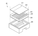
図2はインクジェットヘッド20を示す分解斜視図である。
図2に示すように、インクジェットヘッド20は、ノズル211が設けられたノズルプレート210及び振動板230が設けられた圧力室基板220を、筐体250に嵌め込んで構成されている。このインクジェットヘッド20の主要部構造は、図3の斜視図一部断面図に示すように、圧力室基板220をノズルプレート210と振動板230で挟み込んだ構造を備える。ノズルプレート210は、圧力室基板220と貼り合わせられたときにキャビティ(圧力室)221に対応することとなる位置にノズル211が形成されている。圧力室基板220には、シリコン単結晶基板等をエッチングすることにより、各々が圧力室として機能可能にキャビティ221が複数設けられている。キャビティ221間は側壁(隔壁)222で分離されている。各キャビティ221は、供給口224を介して共通の流路であるリザーバ223に繋がっている。振動板230は、例えば熱酸化膜等により構成される。振動板230にはインクタンク口231が設けられ、後述するタンク81から流路であるパイプ80を通して任意のインクを供給可能に構成されている。振動板230上のキャビティ221に相当する位置には、圧電体素子240が形成されている。圧電体素子240は、PZT素子等の圧電性セラミックスの結晶を上部電極および下部電極(図示せず)で挟んだ構造を備える。圧電体素子240は、制御装置CONTから供給される吐出信号に対応して体積変化を生ずることが可能に構成されている。
【0028】
インクジェットヘッド20からインクを吐出するには、まず、制御装置CONTがインクを吐出させるための吐出信号をインクジェットヘッド20に供給する。インクは、インクジェットヘッド20のキャビティ221に流入しており、吐出信号が供給されたインクジェットヘッド20では、その圧電体素子240がその上部電極と下部電極との間に加えられた電圧により体積変化を生ずる。この体積変化は振動板230を変形させ、キャビティ221の体積を変化させる。この結果、そのキャビティ221のノズル穴211からインクの液滴が吐出される。インクが吐出されたキャビティ221には吐出によって減ったインクが新たにタンクから供給される。
【0029】
なお、前記のインクジェットヘッドは、圧電体素子に体積変化を生じさせてインクを吐出させる構成であったが、発熱体によりインクに熱を加えその膨張によって液滴を吐出させるようなヘッド構成であってもよい。
【0030】
電子天秤(不図示)は、インクジェットヘッド20のノズルから吐出されたインク滴の一滴の重量を測定して管理するために、例えば、インクジェットヘッド20のノズルから、5000滴分のインク滴を受ける。電子天秤は、この5000滴のインク滴の重量を5000の数字とノズル数で割ることにより、1ノズルあたり一滴のインク滴の重量を正確に測定することができる。このインク滴の測定量に基づいて、インクジェットヘッド20から吐出するインク滴の量を最適にコントロールすることができる。
【0031】
クリーニングユニット24は、インクジェットヘッド20のノズル等のクリーニングをデバイス製造工程中や待機時に定期的にあるいは随時に行うことができる。キャッピングユニット22は、インクジェットヘッド20のインク吐出面20Pが乾燥しないようにするために、デバイスを製造しない待機時にこのインク吐出面20Pにキャップをかぶせるものである。
【0032】
インクジェットヘッド20が第2移動装置16によりX軸方向に移動することで、インクジェットヘッド20を電子天秤、クリーニングユニット24あるいはキャッピングユニット22の上部に選択的に位置決めさせることができる。つまり、デバイス製造作業の途中であっても、インクジェットヘッド20を、例えば電子天秤側に移動すれば、インク滴の重量を測定できる。また、インクジェットヘッド20をクリーニングユニット24上に移動すれば、インクジェットヘッド20のクリーニングを行うことができる。インクジェットヘッド20をキャッピングユニット22の上に移動すれば、インクジェットヘッド20のインク吐出面20Pにキャップを取り付けて乾燥を防止する。
【0033】
つまり、これら電子天秤、クリーニングユニット24、及びキャッピングユニット22は、ベース12上の後端側で、インクジェットヘッド20の移動経路直下に、ステージSTと離間して配置されている。ステージSTに対する基板Pの搬入作業及び搬出作業はベース12の前端側で行われるため、これら電子天秤、クリーニングユニット24あるいはキャッピングユニット22により作業に支障を来すことはない。
【0034】
本実施形態に用いられるインクは、特に有機EL装置において基板上に設けられる機能層、すなわち正孔注入層や発光層の形成材料と、有機溶媒あるいは分散媒とを混合してなる液状体の材料、すなわち液体材料である。有機溶媒あるいは分散媒としては、例えば発光層形成材料用の有機溶媒の場合、高沸点の材料が好適に用いられる。このような有機溶媒は、液体材料がインクジェットヘッド20から吐出された後、基板に塗布された液体材料の濡れ広がりを良好にし、直ぐに蒸発するのを抑制するなどの機能を有する。また、形成材料と有機溶媒あるいは分散媒とを混合して調合されたインクは、通常、保管容器に充填された後、真空パックなどの保存処理が施され、その状態で使用時まで保管される。
【0035】
しかしながら、インクの保存期間が長期間に及ぶと、インクの構成材料である形成材料と有機溶媒あるいは分散媒とが相互に影響し、一部の形成材料に変化が生じる。即ち、形成材料の成分である物質が液体材料中で凝集し、形成材料の構成物質と比較して形状の大きい固形物(クラスタ)が生成される。
【0036】
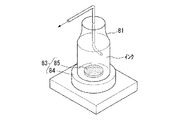
従って、図1に示すように、インクジェットヘッド20には、パイプ(流路)80を介してインクを収容するタンク81が接続されており、更に、延設するパイプ80の中間部には、インク内に含まれるクラスタを除去する濾過装置(除去装置)82が設けられている。タンク81の上部は開口しており、パイプ80の一端は、この開口を介してタンク81内のインクに接続されている。
【0037】
図4に示すように、タンク81には、インクの撹拌装置83が備えられている。撹拌装置83は、例えば、タンク81のステージとなるスターラー84と、タンク81のインク中に配置される撹拌子85とから構成されている。スターラー84は、回転数を自在に変更可能なモータ(不図示)を備えてなり、タンク81の中心軸に対して回転方向に磁場を与え、タンク81内の撹拌子85を磁力により回転させて、インクを撹拌させるものである。
【0038】
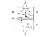
濾過装置82は、図5に示すように、撹拌されたインクが収容される濾過容器90と、該濾過容器90内に設けられるフィルター91とから構成されている。フィルター91は、インク内に含まれるクラスタのみを除去する機能を有するものであり、濾過サイズは、0.5μm以下とすることが好ましく、さらには、0.2μm以下とすることがより好ましい。
【0039】
次に、上述したインクジェット装置IJを用いて、ステージSTに支持されている基板Pに対してインクジェットヘッド20からインクを吐出することにより、基板P上にパターンを形成する方法について説明する。なお、ここで吐出するインクは、後述する有機EL装置における機能層、すなわち発光層あるいは正孔注入層、さらには電子注入層の形成材料を、溶媒に溶解させあるいは分散媒に分散させてなる液体材料である。
【0040】
まず、タンク81には、機能層の形成材料と、有機溶媒(あるいは分散媒)とを混合して調合されたインク(液体材料)が収容される。タンク81をスターラー84上に載置し、スターラー84を駆動させることにより、タンク81のインク中に配置された撹拌子85が回転し、インクが撹拌され、インク含まれる原液と有機溶媒とは、タンク81内で均一に分散される。
【0041】
次いで、撹拌されたインクは、パイプ80を通過して、濾過装置82に備えられた濾過容器90に収容される。撹拌後のインクを、濾過容器90内のフィルター91を通過させることにより、インク内にクラスタが生成されていた場合、クラスタは、フィルター91を通過することができずに捕獲され、インクが供給された濾過容器90内の第1の領域に留まり、凝集が生じていない原料と有機溶媒のみがフィルター91を通過し、インクジェットヘッド20に通ずる濾過容器90内の第2の領域に移動する。
【0042】
制御装置CONTは、インクジェットヘッド20を駆動し、脱気されたインクをステージSTに支持されている基板Pに対して吐出する。
【0043】
以上説明したように、インクを収容するタンク81とインクジェットヘッド20との間に、濾過装置82を設けることにより、一定期間保管され、クラスタが含まれるインクを使用しても、濾過装置82内でインク中からクラスタのみが除去される。また、タンク81に撹拌装置83を設けることにより、インク中に含まれる原料や有機溶媒を効率良く均一に分散させるので、濾過装置82では、クラスタを効率良く捕獲することができる。
【0044】
これにより、液体材料にクラスタが含まれることに起因する、有機EL装置の初期特性や寿命特性の低下を防止することが可能となり、更に、粒径の大きいクラスタに起因するノズル詰まりなどといった不具合の発生を防止しつつ安定した吐出動作を実現できる。
【0045】
なお、本実施形態では、クラスタを除去する装置としてフィルターを備えた濾過装置としたが、インク中のクラスタを効率良く除去することができるものであれば、フィルター方式の濾過装置に限定するものではない。
また、タンク内のインクの撹拌装置として、スターラーと撹拌子を用いたが、撹拌装置もこれに限定するものではなく、例えば、超音波装置によりインクに低振動を与えて、インク中の構成材料を均一に分散させてもよい。
【0046】
本発明の有機EL装置の製造装置、すなわちインクジェット装置(液滴吐出製造装置)IJからなる製造装置は、特に有機エレクトロルミネッセンス装置(有機EL装置)における機能層の形成に好適に用いられるものである。
図6は、有機EL装置の一例を示す断面図である。図6において、有機EL装置301は、基板302と、基板302の一方の面側に設けられ一対の陰極(電極)307及び陽極(電極)308と、これら電極307、308間に狭持された機能層309と、基板302と機能層309との間に設けられた封止層304と、を備えて構成されたものである。機能層309は、本例では有機エレクトロルミネッセンス材料からなる発光層305と、正孔注入層306とからなっている。
【0047】
ここで、図6に示す有機EL装置301は、発光層305からの発光光を基板302を構成する材料側から装置外部に取り出す形態であり、基板302は、光を透過可能な透明あるいは半透明材料に少なくとも光を透過可能な透明あるいは半透明な陽極308を形成したものである。本実施形態では省略してあるが、基板302に配線、あるいは、薄膜トランジスタを形成してあるものでもよい。光を透過可能な透明あるいは半透明材料としては、例えば、透明なガラス、石英、サファイア、あるいはポリエステル、ポリアクリレート、ポリカーボネート、ポリエーテルケトンなどの透明な合成樹脂などが挙げられる。特に、基板302の形成材料としては、安価なソーダガラスが好適に用いられる。
陽極308は、インジウム錫酸化物(Indium Tin Oxide:ITO)等からなる透明電極であって光を透過可能なものである。
一方、基板を構成する材料と反対側から発光光を取り出す形態の場合には、基板を構成する材料は不透明であってもよく、その場合、アルミナ等のセラミック、ステンレス等の金属シートに表面酸化などの絶縁処理を施したもの、熱硬化性樹脂、熱可塑性樹脂などを用いることができる。この場合、陽極308は光を透過可能でなくてもよい。
【0048】
また、正孔注入層306は、特に、発光層305の発光効率、寿命などの素子特性を向上させる機能を有する。正孔注入層306を形成するための材料(形成材料)としては、例えば、ポリチオフェン誘導体、ポリピロール誘導体など、または、それらのドーピング体などが採用される。特に、3,4−ポリエチレンジオキシチオフェン/ポリスチレンスルフォン酸(PEDOT/PSS)の分散液、すなわち、分散媒としてのポリスチレンスルフォン酸に3,4−ポリエチレンジオキシチオフェンを分散させ、さらにこれを水に分散させた分散液が好適に用いられる。
【0049】
また、正孔注入層に代えて正孔輸送層を形成しても良く、さらに正孔注入層と正孔輸送層を両方形成するようにしても良い。その場合、正孔輸送層を形成するための材料は、正孔を輸送できれば周知のどのような正孔輸送材料であっても良く、例えば、そのような材料として、アミン系、ヒドラゾン系、スチルベン系、スターバスト系などに分類される有機材料が種々知られている。正孔注入層と正孔輸送層を両方形成する場合には、例えば、正孔輸送層の形成に先立って、正孔注入層を陽極側に形成し、その上に正孔輸送層を形成するのが好ましい。このように正孔輸送層を正孔注入層とともに形成することにより、駆動電圧の上昇を制御することができるとともに、駆動寿命(半減期)を長くすることが可能となる。
【0050】
発光層305の形成材料としては、低分子の有機発光色素や高分子発光体、即ち、各種の蛍光物質や燐光物質などの発光物質、Alq3(アルミキレート錯体)などの有機エレクトロルミネッセンス材料が使用可能である。発光物質となる共役系高分子の中ではアリーレンビニレン又はポリフルオレン構造を含むものなどが特に好ましい。低分子発光体では、例えばナフタレン誘導体、アントラセン誘導体、ペリレン誘導体、ポリメチン系、キサテン系、クマリン系、シアニン系などの色素類、8−ヒドロキノリンおよびその誘導体の金属錯体、芳香族アミン、テトラフェニルシクロペンタジエン誘導体等、又は特開昭57−51781、同59−194393号公報等に記載されている公知のものが使用可能である。陰極7はアルミニウム(Al)やマグネシウム(Mg)、金(Au)、銀(Ag)等からなる金属電極である。
【0051】
なお、陰極307と発光層305との間に、電子輸送層や電子注入層を設けることができる。電子輸送層の形成材料としては、特に限定されることなく、オキサジアゾール誘導体、アントラキノジメタンおよびその誘導体、ベンゾキノン及びその誘導体、ナフトキノンおよびその誘導体、アントラキノン及びその誘導体、テトラシアノアンスラキノジメタン及びその誘導体、フルオレノン誘導体、ジフェニルジシアノエチレン及びその誘導体、ジフェノキノン誘導体、8−ヒドロキシキノリン及びその誘導体の金属錯体等が例示される。
【0052】
封止層304は、基板302側の外部から電極307,308を含む機能層309に対して大気が侵入するのを遮断するものであって、膜厚や材料を適宜選択することにより光を透過可能となっている。封止層304を構成する材料としては、例えばセラミックや窒化珪素、酸化窒化珪素、酸化珪素などの透明な材料が用いられ、中でも酸化窒化珪素が透明性、ガスバリア性の観点から好ましい。なお、封止層304の厚さは発光層305から射出される光の波長より小さくなるように設定されるものが好ましい(例えば0.1μm)。
【0053】
図示しないが、この有機EL装置301はアクティブマトリクス型であり、実際には複数のデータ線と複数の走査線とが格子状に配置され、これらデータ線や走査線に区画されたマトリクス状に配置された画素毎に、スイッチングトランジスタやドライビングトランジスタ等の駆動用TFTを介して前記の機能層309が接続されている。そして、データ線や走査線を介して駆動信号が供給されると電極間に電流が流れ、機能層309の発光層305が発光して基板302の外面側に光が射出され、その画素が点灯する。
【0054】
また、有機EL装置301のうち、機能層309を挟んで封止層304と反対側の表面にも、電極307,308を含む機能層309に対して大気が侵入するのを遮断する封止部材310が形成されている。
【0055】
以上説明した有機EL装置301の機能層309、すなわち発光層305,正孔注入層306などの形成材料を、有機溶媒あるいは分散媒でインク化(液体材料化)し、このインク(液体材料)をタンク81に収容して撹拌し、その後濾過処理を行うことにより、前述したようにノズル詰まりなどの不具合の発生を防止しつつ、初期特性や寿命特性の向上した有機EL装置301を製造することができる。
【0056】
前記有機EL装置を備えた電子機器の例について説明する。
図7は、携帯電話の一例を示した斜視図である。図7において、符号1000は携帯電話本体を示し、符号1001は前記の有機EL装置を用いた表示部を示している。
【0057】
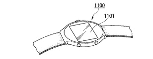
図8は、腕時計型電子機器の一例を示した斜視図である。図8において、符号1100は時計本体を示し、符号1101は前記の有機EL装置を用いた表示部を示している。
【0058】
図9は、ワープロ、パソコンなどの携帯型情報処理装置の一例を示した斜視図である。図9において、符号1200は情報処理装置、符号1202はキーボードなどの入力部、符号1204は情報処理装置本体、符号1206は前記の有機EL装置を用いた表示部を示している。
【0059】
図7〜図9に示す電子機器は、前記実施の形態の有機EL装置を表示部として備えているので、これら電子機器自体も、特にその表示部の初期特性や寿命特性が良好なものとなる。
【0060】
次に、インク(液体材料)に濾過処理を施した場合の効果を確認するための実験及び結果について説明する。
まず、有機EL装置の正孔注入層を形成するべく、ITO基板上に、機能層(正孔注入層)の形成材料をPEDOT/PSSとしたインク(液体材料)を成膜し、更にこの膜上にアルミニウム層を形成した。組成比の異なるインクを2種類使用して、インクの保存期間に対する素子の初期抵抗値と、駆動寿命を確認した。
【0061】
インクに含まれる有機溶媒は、NMP(N−メチル−2−ピロリジノン)と、DMI(1,3−ジメチル−2−イミダゾリジノン)の2種類を採用した。また、PEDOT/PSSにおけるPEDOTとPSSの混合比は、1:20と設定した。インクの組成比は、第1のインク(以下、PEDOT1と表記する)をPEDOT/PSS:NMP:DMI=22.4:27.6:50とし、第2のインク(以下、PEDOT2と表記する)をPEDOT/PSS:NMP:DMI=14:22:50と設定した。
【0062】
図10に示すように、インクを生成した後の保存期間が長期間になるにつれて、PEDOT1、2は、ともに素子の初期抵抗値が上昇することがわかる。更に、図11に示すように、インクの保存期間が長期間になるにつれて、PEDOT1、2は、ともに素子の寿命が低下することがわかる。これは、一部のPEDOT/PSSから、PSSと水分とが有機溶媒のNMPとDMI中に溶解し、成分が溶解したPEDOT/PSSが凝集したクラスタが発生したことに起因して、原料全体の成分構成が変化したことを意味する。
【0063】
次に、前記のPEDOT1、2に対して濾過処理を行うことにより、インク中に生成されたクラスタを除去した。濾過装置に備えたフィルターの濾過サイズは、0.2μmである。
【0064】
図12に示すように、濾過容器90内の撹拌後のインクが流入する領域100において、生成されたクラスタは、フィルター91で捕獲される。そして、PSSと水分とを溶解していない、正常なPEDOT/PSSは、フィルター91を通過して、インクジェットヘッド20に接続される領域101に移動することができる。
【0065】
これにより、保存期間が25日目のPEDOT1及びPEDOT2を用いて形成された膜の初期抵抗値は、PEDOT2とPEDOT1とを比較すると初期抵抗値が約23分の1となった。特に、駆動寿命は、インクの撹拌と濾過処理を施すことによって、約5倍に向上した。
【0066】
次に、本発明のイオン性不純物の除去方法について説明する。この方法は、特に前記のインクジェット装置IJのインクジェットヘッド20から液体材料、例えば前述したような有機EL装置301における機能層309の形成材料を含む液体材料を吐出するに先立って行われる方法である。
すなわち、この方法では、前記液体材料に含まれているイオン性不純物を、イオン交換材料でイオン交換することによって除去するようにした方法である。
【0067】
イオン性不純物としては、カチオン(陽イオン)やアニオン(陰イオン)があり、処理対象となる液体材料に応じてイオン交換材料が適宜に選択され用いられる。なお、カチオンとしては各種の金属イオンが挙げられ、具体的には周期律表Ia族、IIa族、VIa族、VIIa族、およびIIb族に属する金属のイオンが挙げられる。また、アニオンとしては、硫酸イオン(SO4 2−)、ギ酸イオン(HCO2 −)、シュウ酸イオン(C2H4 2−)、酢酸イオン(CH3COO−)等の無機イオンおよび有機イオンが挙げられる。
【0068】
イオン交換材料としては、イオン交換樹脂や無機イオン交換材料が用いられ、さらには機械的な濾過機能をも有するイオン交換材料も好適に用いられる。
イオン交換樹脂として、特にカチオン除去用のもの、すなわち陽イオン交換樹脂としては、例えば、強酸性イオン交換樹脂、弱酸性イオン交換樹脂、重金属を選択的に除去し得るキレート樹脂等があり、これらは、例えばスチレン系、メタクリル系、アクリル系等の各種ポリマーの主鎖に、−SO3M、−COOM、−N=(CH2COO)2M等の各種の官能基が導入されてなるものである。なお、官能基については、陽イオン交換樹脂の種類等に応じて適宜に選択される。
【0069】
一方、アニオン除去用のもの、すなわち陰イオン交換樹脂としては、例えば、最強塩基性陰イオン交換樹脂、強塩基性陰イオン交換樹脂、中塩基性陰イオン交換樹脂、弱塩基性陰イオン交換樹脂等があり、これらは、例えばスチレン系、アクリル系等の各種ポリマーの主鎖に、第4級アンモニウム塩基、第3級アミン等の各種の官能基が導入されてなるものである。なお、官能基は、陰イオン交換樹脂の種類等に応じて適宜に選択される。
【0070】
これらイオン交換樹脂は、繊維状、あるいはこの繊維からなる織布、不織布、さらには粒状のものや各種の形状に成形されてなる成形体として用いられ、繊維状のものや織布、不織布からなるフィルター状のもの、さらには粒状のものなどは、例えば図1に示したインクジェット装置IJにおいて、特に図5に示した濾過装置82にフィルター91に代えて充填され、用いられる。このようにフィルター91に代えてイオン交換樹脂を充填することにより、この濾過装置82は、イオン性不純物除去装置として機能するようになる。
【0071】
すなわち、例えば有機EL装置の機能層形成材料、例えば正孔注入層の形成材料や発光層形成材料を有機溶媒に溶解し、あるいは分散媒に分散させてなる液体材料をこのイオン性不純物除去装置(濾過装置82)に通過させることにより、この液体材料中のイオン性不純物、例えば発光層形成材料や正孔注入層形成材料に由来する金属イオンや、正孔注入層の形成材料である(PEDOT/PSS)中のポリスチレンスルフォン酸に由来する硫酸イオン(SO4 2−)をイオン交換し、除去することができる。
【0072】
また、無機イオン交換材料は、金属酸化物など金属塩からなるもので、陽イオンを吸着してイオン交換するタイプと陰イオンを吸着してイオン交換するタイプと、陽イオン、陰イオンを共に吸着してイオン交換するタイプとがある。
陽イオンをイオン交換するタイプの無機イオン交換材料としては、五酸化アンチモン(Sb2O5)の水和物(例えば、東亜合成株式会社製のIXE[登録商標]−300)やリン酸チタン(例えば、東亜合成株式会社製のIXE[登録商標]−400)、リン酸ジルコニウム(例えば、東亜合成株式会社製のIXE[登録商標]−100)などがある。特に、五酸化アンチモンの水和物はNaイオンに対する吸着選択性が高いことから、前記正孔注入層の形成材料(PEDOT/PSS)を含有した液体材料に対する無機イオン交換材料として、好適とされる。なぜなら、正孔注入層形成材料にはイオン性不純物としてNaイオンが多く含有されているからである。
【0073】
また、陰イオンをイオン交換するタイプの無機イオン交換材料としては、含水酸化ビスマス(例えば、東亜合成株式会社製のIXE[登録商標]−500)や水酸化リン酸鉛(例えば、東亜合成株式会社製のIXE[登録商標]−1000)などがある。特に含水酸化ビスマスは、硫酸イオン(SO4 2−)に対する吸着選択性が高いことから、前記正孔注入層の形成材料(PEDOT/PSS)を含有した液体材料に対する無機イオン交換材料として、前記五酸化アンチモンの水和物とともに好適に用いられる。すなわち、前記正孔注入層形成材料は、分散媒としてポリスチレンスルフォン酸を用いていることから、特にNaイオンが前記五酸化アンチモンの水和物にイオン交換されると、これによって硫酸イオンが遊離するからである。
【0074】
また、陽イオン、陰イオンを共に吸着してイオン交換するタイプとしては、酸化ジルコニウムや含水酸化ジルコニウム、含水酸化チタン、さらにはアンチモン、ビスマス系のもの(例えば、東亜合成株式会社製のIXE[登録商標]−600やIXE[登録商標]−633)などがある。このようなタイプのものを用いれば、前述した本来の正孔注入/輸送層形成材料中に含まれるNaイオンをイオン交換すると同時に、遊離した硫酸イオンをイオン交換することも期待することができる。
【0075】
これら無機イオン交換材料は粒状または粉末状のものであり、先のイオン交換樹脂の場合と同様に、図1に示したインクジェット装置IJにおいて、特に図5に示した濾過装置82にフィルター91に代えて充填され、用いられる。このようにフィルター91に代えて無機イオン交換材料を充填することにより、この濾過装置82は、先のイオン交換樹脂の場合と同様に、イオン性不純物除去装置として機能するようになる。
【0076】
また、これらイオン交換樹脂や無機イオン交換樹脂は、イオン交換能を有し、したがってイオン性不純物を選択的に除去するようになっているものの、固形物、例えば前記のクラスタを機械的に濾過する機能は有していない。そこで、特にこのイオン性不純物の除去方法をデバイスの製造方法、例えば有機EL装置の製造方法に適用すべく、前記の図1に示したインクジェット装置IJに用いる場合、前述したようにフィルター91に代えてイオン交換材料(イオン交換樹脂や無機イオン交換材料)を充填した濾過装置82を用いると同時に、フィルター91を充填した濾過装置82も用いることで、クラスタとイオン性不純物との両方を除去するのが好ましい。
【0077】
具体的には、図13に示すようにタンク81にフィルター91を充填した濾過装置82をパイプ80で接続し、さらにこの濾過装置82に、フィルター91に代えてイオン交換材料(イオン交換樹脂や無機イオン交換材料)を充填したイオン性不純物除去装置82aをパイプ80で接続することにより、クラスタとイオン性不純物との両方を除去することができる。すなわち、タンク81に貯留した液体材料(機能層形成材料を含有してなる液体材料)に対して、その中に含まれるクラスタ等の固形物を濾過装置82で機械的に濾過し、さらにイオン性不純物除去装置82aでイオン性不純物も除去することにより、十分に精製された液体材料を形成することができる。したがって、この液体材料をインクジェットヘッド20から吐出することにより、良好な機能層を形成することができ、これによりクラスタやイオン性不純物といった不純物に起因して機能層の機能が低下するのを防止することができる。
【0078】
なお、フィルター91を充填した濾過装置82において、フィルター91の上側またはその下側にイオン交換材料(イオン交換樹脂や無機イオン交換材料)を設けることにより、一つの濾過装置82にイオン性不純物の除去機能も付加することができる。したがって、これを用いても良好な機能層を形成することができ、これによりクラスタやイオン性不純物といった不純物に起因して機能層の機能が低下するのを防止することができる
【0079】
また、イオン交換材料としては、前記のイオン交換樹脂や無機イオン交換材料に代えて、機械的な濾過機能を有するイオン交換材料を用いることもできる。この濾過機能を有するイオン交換材料としては、例えばポリエチレン多孔質膜にカチオン交換基あるいはアニオン交換基を化学的に修飾したフィルターが用いられ、具体的には日本ポール株式会社製のイオンクリーン[商品名]などが好適に用いられる。このものは、ポリエチレン膜の微細な孔内部にイオン交換基を修飾したもので、対流支援効果により、液体材料中からイオン性不純物となる金属イオンを迅速に除去するものである。
【0080】
また、セルロース繊維、酸洗浄済み珪藻土およびレジンからなるものや、さらにこれらに強イオン交換樹脂を含有させてなるものを用いることができる。その場合、具体的には日本ポール株式会社製のイオンクリーン[商品名]などが好適に用いられる。
これらイオン交換材料、すなわち機械的な濾過機能を有するイオン交換材料にあっては、これを図1に示したインクジェット装置IJにおいて、特に図5に示した濾過装置82にフィルター91に代えて充填し、用いることができる。このようにフィルター91に代えて濾過機能を有するイオン交換材料を充填することにより、この濾過装置82は、単にイオン性不純物除去装置として機能するだけでなく、クラスタ等の固形物を機械的に濾過する機能を有したものとなる。
【0081】
したがって、この濾過装置82(フィルター91に代えて機械的な濾過機能を有するイオン交換材料を充填したもの)に液体材料、例えば前記の有機EL装置の機能層形成材料を含有した液体材料を通過させることにより、この液体材料中のイオン性不純物はもちろん、クラスタ等の固形物も同時に除去することができる。よって、この液体材料をインクジェットヘッド20から吐出することにより、良好な機能層を形成することができ、これによりクラスタやイオン性不純物といった不純物に起因して機能層の機能が低下するのを防止することができる。
【0082】
なお、前記実施形態では、本発明のイオン性不純物の除去方法を特に有機EL装置における機能層(発光層、正孔輸送層)の形成に適用する場合について述べたが、本発明はこれに限定されることなく、液晶装置や半導体装置など種々のデバイスにおける各種機能層の形成材料や、さらには各種の薬品など、液滴吐出ヘッドから吐出される全ての液体材料に対する精製に適用することができる。
【0083】
【発明の効果】
以上説明したように本発明の有機EL装置の製造方法は、液体材料を液滴吐出ヘッドに供給する前に、液体材料に含まれているクラスタを除去し、クラスタが除去された液体材料を液滴吐出ヘッドより吐出するようにした方法であるから、液体材料中にクラスタが含まれることに起因する、有機EL装置の初期特性や寿命特性の低下を防止することができ、したがって信頼性の高い有機EL装置を提供することができる。
【0084】
また、本発明のイオン性不純物の除去方法は、液滴吐出ヘッドから液体材料を吐出するに先立ち、前記液体材料に含まれているイオン性不純物を、イオン交換材料でイオン交換することによって除去するようにした方法であるから、液体材料中にイオン性不純物が含まれることに起因する不都合を防止することができ、したがってこの液体材料から形成する要素のイオン性不純物に起因する機能低下を防止することができる。
【図面の簡単な説明】
【図1】本発明の製造装置の一実施形態を示す概略斜視図である。
【図2】インクジェットヘッドの分解斜視図である。
【図3】インクジェットヘッドの主要部の斜視図一部断面図である。
【図4】タンク近傍の拡大斜視図である。
【図5】濾過装置近傍の拡大斜視図である。
【図6】有機EL装置を示す概略断面図である。
【図7】有機EL装置が搭載された電子機器を示す図である。
【図8】有機EL装置が搭載された電子機器を示す図である。
【図9】有機EL装置が搭載された電子機器を示す図である。
【図10】本発明の製造方法の効果を確認するための測定結果を示す図である。
【図11】本発明の製造方法の効果を確認するための測定結果を示す図である。
【図12】濾過装置におけるクラスタの除去を説明する概念図である。
【図13】イオン性不純物除去装置を用いた例を示す図である。
【符号の説明】
20…インクジェットヘッド(液滴吐出ヘッド)、81…タンク(容器)、
82…濾過装置、82a…イオン性不純物除去装置、83…撹拌装置、
301…有機EL装置、305…発光層、306…正孔注入層、
IJ…インクジェット装置(液滴吐出装置、製造装置)[0001]
BACKGROUND OF THE INVENTION
The present inventionYesMachine equipment manufacturing equipmentPlaceAbout.
[0002]
[Prior art]
In recent years, in a method for manufacturing a device having a fine wiring pattern such as a semiconductor integrated circuit or a method for manufacturing an electro-optical device in which a functional layer such as a transparent electrode or a light emitting layer is formed on a substrate, a droplet discharge method such as an ink jet method is used. Attention has been focused on a method of forming a wiring or film using a film. As a method using such a droplet discharge method, for example, a technique relating to a method for manufacturing an electric circuit using an inkjet method is disclosed (for example, see Patent Document 1). This disclosed technique forms an electric circuit by ejecting a fluid containing a pattern forming material on the pattern forming surface from an ink jet head, and is extremely difficult in that it can be used for a small amount of various types of production. It is valid.
[0003]
[Patent Document 1]
Japanese Patent Laid-Open No. 11-274671
[0004]
[Problems to be solved by the invention]
By the way, normally, the liquid material discharged from the ink jet head is formed by mixing various functional layer forming materials such as wiring to be patterned on a substrate or a thin film to be formed, and an organic solvent or a dispersion medium. However, for example, when the storage period of the liquid material before ejection extends for a long time, the form of the liquid material may change due to the solvent or the dispersion medium. Specifically, clusters and ionic impurities may occur in the liquid material. In addition, a device such as an organic EL device formed of a liquid material in which the form is changed and clusters or ionic impurities are generated has a problem that initial characteristics and life characteristics are deteriorated.
[0005]
The present invention has been made in view of such circumstances. For example, when an organic EL device is manufactured using a droplet discharge method such as an ink jet method, the initial characteristics and life characteristics can be improved.YesMachine equipment manufacturing equipmentPlaceThe purpose is to provide.
[0006]
[Means for Solving the Problems]
In order to solve the above-described problems, a method for manufacturing an organic EL device according to the present invention is a method for manufacturing an organic EL device including a functional layer having at least a light emitting layer between a pair of electrodes. Forming the functional layer by discharging a liquid material obtained by dissolving the forming material of the functional layer in a solvent or dispersing in a dispersion medium from the droplet discharge head. The process includes storing the liquid material in a container, removing the clusters contained in the liquid material before supplying the liquid material from the container to the droplet discharge head, and removing the clusters from the liquid material. The material is discharged from the droplet discharge head.
According to the above method, before supplying the liquid material to the droplet discharge head, the clusters contained in the liquid material are removed, and the liquid material from which the clusters have been removed is discharged from the droplet discharge head. It is possible to prevent the deterioration of the initial characteristics and life characteristics of organic EL devices due to the inclusion of clusters in the material, and also prevent the occurrence of problems such as nozzle clogging due to clusters with large particle sizes. In addition, a stable discharge operation can be realized.
In addition, the said cluster means the whole solid substance produced | generated by the chemical change in a liquid material, a mass transfer, or a shape change.
[0007]
Moreover, in the said manufacturing method, it is preferable that the said cluster is removed by filtering the said liquid material.
Thereby, the clusters contained in the liquid material are efficiently removed.
[0008]
The functional layer includes a hole injection layer, and a liquid material obtained by dissolving the material for forming the hole injection layer in a solvent or dispersing in a dispersion medium is discharged from a droplet discharge head to the substrate. The step of forming the hole injection layer includes the step of storing the liquid material in a container and supplying the liquid material from the container to the droplet discharge head. Further, it is characterized in that clusters contained in the liquid material are removed, and the liquid material from which the clusters have been removed is ejected from the droplet ejection head.
In this way, for example, polyethylene geodioxide can be used as a liquid material in which the hole injection layer forming material is dissolved or dispersed.KiEven when a dispersion of thiothiophene / polystyrene sulfonic acid (PEDOT / PSS) is used, removal of clusters caused by this prevents the deterioration of the initial characteristics and lifetime characteristics of the resulting organic EL device. It becomes possible to do.
[0009]
Moreover, in the said manufacturing method, it is preferable to stir the said liquid material within the said container before removing the said cluster.
In this way, since the liquid material is agitated in the container in advance, it becomes possible to efficiently remove the clusters contained in the liquid material thereafter.
[0010]
In the manufacturing method, the cluster may be a solid material formed by aggregating the forming material of the functional layer formed on the substrate in the liquid material before discharging.
In this way, it is possible to further prevent deterioration of the initial characteristics and life characteristics of the organic EL device due to the inclusion of clusters in the functional layer forming material in the liquid material.
[0011]
An organic EL device manufacturing method of the present invention is an organic EL device manufacturing apparatus including a functional layer having at least a light emitting layer and a hole injection layer between a pair of electrodes, A droplet discharge head that discharges a liquid material in which a functional layer forming material is dissolved in a solvent or dispersed in a dispersion medium; and a container that contains the liquid material and is connected to the droplet discharge head. The ionic impurities provided between the container and the droplet discharge head and contained in the liquid material are ion-exchanged by an ion exchange material having a mechanical filtration function and are contained in the liquid material. And a removal device that removes the clusters that are removed by the ion exchange material, and the liquid material accommodated in the container is a liquid material obtained by dispersing the formation material of the hole injection layer in a dispersion medium , The material for forming the hole injection layer is 3,4-polyethylenedioxythiophene / polystyrene sulfonic acid, and the dispersion medium for the hole injection layer is at least N-methyl-2-pyrrolidinone and 1,3-dimethyl- It includes 2-imidazolidinone, and the removal device has a filter that removes the cluster, and a filtration size of the filter is 0.5 μm or less.
An organic EL device manufacturing apparatus of the present invention is an organic EL device manufacturing device including a functional layer having at least a light-emitting layer between a pair of electrodes, and a material for forming the functional layer with respect to a substrate. A droplet discharge head that discharges a liquid material dissolved in a solvent or dispersed in a dispersion medium, a container that accommodates the liquid material and is connectable to the droplet discharge head, and the container and the liquid And a device for removing clusters contained in the liquid material, which is provided between the liquid droplet ejection head and the liquid droplet ejection head.
According to the above apparatus, the liquid material is contained in the container connected to the droplet discharge head, and the cluster contained in the liquid material in the cluster removing apparatus provided between the container and the droplet discharge head. Therefore, it is possible to prevent deterioration of the initial characteristics and life characteristics of the device due to the inclusion of clusters in the liquid material, and further nozzle clogging due to clusters having a large particle size, etc. A stable discharge operation can be realized while preventing the occurrence of defects.
[0012]
Moreover, in the said manufacturing apparatus, it is preferable that the said removal apparatus is a filtration apparatus.
In this way, the clusters contained in the liquid material can be removed efficiently and at low cost.
[0013]
In the manufacturing apparatus, it is preferable that an ionic impurity removing device is provided between the container and the droplet discharge head.
In this way, not only clusters but also ionic impurities can be removed.
[0014]
Moreover, in the said manufacturing apparatus, it is preferable that at least one part of the said removal apparatus is formed with the ion exchanger.
In this way, ionic impurities can also be removed by ion exchange using an ion exchanger.
[0015]
Moreover, in the said manufacturing apparatus, it is preferable that the said container is provided with the stirring apparatus or the ultrasonic apparatus.
In this way, the liquid material is agitated in the container before the liquid material is moved from the container to the removal device, and the clusters are uniformly dispersed in the liquid material. Therefore, the clusters are efficiently dispersed in the removal device. It becomes possible to make it.
[0016]
An electronic apparatus according to the present invention includes an organic EL device obtained by the above manufacturing method or an organic EL device manufactured by the manufacturing device.
According to this electronic apparatus, since the organic EL device in which deterioration of initial characteristics and life characteristics is prevented is provided, the electronic equipment itself also has good initial characteristics and life characteristics.
[0017]
In the method for removing ionic impurities of the present invention, prior to discharging the liquid material from the droplet discharge head, the ionic impurities contained in the liquid material are removed by ion exchange with an ion exchange material. It is a feature.
According to this ionic impurity removal method, the ionic impurities contained in the liquid material are removed by ion exchange, so that inconvenience caused by the ionic impurities contained in the liquid material can be prevented. Is possible.
[0018]
DETAILED DESCRIPTION OF THE INVENTION
The present invention will be described below with reference to the drawings.
FIG. 1 is a schematic perspective view showing an embodiment of an apparatus for manufacturing an organic EL device according to the present invention and showing an ink jet device (droplet discharge device) having an ink jet head (droplet discharge head). In addition, this inkjet apparatus becomes a manufacturing apparatus of the organic EL apparatus of this invention.
[0019]
In FIG. 1, an inkjet apparatus IJ is provided on a
[0020]
The first moving
[0021]
The first moving
[0022]
The
[0023]
The stage ST holds the substrate P and positions it at a predetermined position. Further, the stage ST has a
[0024]
The second moving
[0025]
The
[0026]
1 can be positioned by linearly moving in the Z-axis direction in the
[0027]
FIG. 2 is an exploded perspective view showing the
As shown in FIG. 2, the
[0028]
In order to eject ink from the
[0029]
The inkjet head described above has a configuration in which ink is ejected by causing a volume change in the piezoelectric element, but a head configuration in which heat is applied to the ink by a heating element and droplets are ejected by expansion thereof. May be.
[0030]
The electronic balance (not shown) receives, for example, 5000 drops of ink droplets from the nozzles of the
[0031]
The
[0032]
By moving the
[0033]
That is, the electronic balance, the
[0034]
The ink used in this embodiment is a liquid material formed by mixing a functional layer provided on a substrate in an organic EL device, that is, a material for forming a hole injection layer or a light emitting layer, and an organic solvent or dispersion medium. That is, it is a liquid material. As the organic solvent or dispersion medium, for example, in the case of an organic solvent for a light emitting layer forming material, a high boiling point material is preferably used. Such an organic solvent has a function of improving the wetting and spreading of the liquid material applied to the substrate after the liquid material is ejected from the
[0035]
However, when the storage period of the ink is extended for a long time, the forming material which is a constituent material of the ink and the organic solvent or the dispersion medium influence each other, and a part of the forming material is changed. That is, substances that are components of the forming material aggregate in the liquid material, and solids (clusters) having a shape larger than that of the constituent material of the forming material are generated.
[0036]
Accordingly, as shown in FIG. 1, a
[0037]
As shown in FIG. 4, the
[0038]
As shown in FIG. 5, the
[0039]
Next, a method for forming a pattern on the substrate P by ejecting ink from the
[0040]
First, the
[0041]
Next, the stirred ink passes through the
[0042]
The control device CONT drives the
[0043]
As described above, by providing the
[0044]
As a result, it is possible to prevent deterioration of the initial characteristics and life characteristics of the organic EL device due to the inclusion of clusters in the liquid material, and further problems such as nozzle clogging due to clusters having a large particle diameter. A stable discharge operation can be realized while preventing the occurrence.
[0045]
In the present embodiment, the filtering device is provided with a filter as a device for removing the clusters. However, the filtering device is not limited to the filtering method as long as the clusters in the ink can be efficiently removed. Absent.
Further, although a stirrer and a stirrer are used as a stirrer for the ink in the tank, the stirrer is not limited to this. For example, a low vibration is applied to the ink by an ultrasonic device, and the constituent material in the ink May be dispersed uniformly.
[0046]
The manufacturing apparatus of the organic EL device of the present invention, that is, the manufacturing apparatus composed of the ink jet apparatus (droplet discharge manufacturing apparatus) IJ is particularly suitable for forming a functional layer in an organic electroluminescence apparatus (organic EL apparatus). .
FIG. 6 is a cross-sectional view showing an example of an organic EL device. In FIG. 6, the
[0047]
Here, the
The
On the other hand, in the case where emitted light is extracted from the side opposite to the material constituting the substrate, the material constituting the substrate may be opaque. In this case, the surface is oxidized on a ceramic sheet such as alumina or a metal sheet such as stainless steel. It is possible to use an insulating treatment such as a thermosetting resin or a thermoplastic resin. In this case, the
[0048]
In addition, the
[0049]
Further, a hole transport layer may be formed instead of the hole injection layer, and both the hole injection layer and the hole transport layer may be formed. In that case, the material for forming the hole transporting layer may be any known hole transporting material as long as it can transport holes. Examples of such a material include amine, hydrazone, stilbene. Various organic materials classified into a system, a starbust system, and the like are known. When forming both the hole injection layer and the hole transport layer, for example, prior to the formation of the hole transport layer, the hole injection layer is formed on the anode side, and the hole transport layer is formed thereon. Is preferred. By forming the hole transport layer together with the hole injection layer in this way, it is possible to control the increase in drive voltage and to extend the drive life (half life).
[0050]
As a material for forming the
[0051]
Note that an electron-transporting layer or an electron-injecting layer can be provided between the
[0052]
The
[0053]
Although not shown, this
[0054]
Further, in the
[0055]
The forming materials such as the
[0056]
An example of an electronic apparatus provided with the organic EL device will be described.
FIG. 7 is a perspective view showing an example of a mobile phone. In FIG. 7,
[0057]
FIG. 8 is a perspective view showing an example of a wristwatch type electronic apparatus. In FIG. 8,
[0058]
FIG. 9 is a perspective view showing an example of a portable information processing apparatus such as a word processor or a personal computer. In FIG. 9,
[0059]
Since the electronic devices shown in FIGS. 7 to 9 include the organic EL device of the above-described embodiment as a display unit, these electronic devices themselves have particularly good initial characteristics and life characteristics of the display unit. .
[0060]
Next, an experiment and results for confirming the effect when the ink (liquid material) is filtered will be described.
First, in order to form a hole injection layer of an organic EL device, an ink (liquid material) whose functional layer (hole injection layer) is made of PEDOT / PSS is formed on an ITO substrate. An aluminum layer was formed on top. Two types of inks having different composition ratios were used, and the initial resistance value of the element with respect to the ink storage period and the driving life were confirmed.
[0061]
Two types of organic solvents included in the ink were used: NMP (N-methyl-2-pyrrolidinone) and DMI (1,3-dimethyl-2-imidazolidinone). Moreover, the mixing ratio of PEDOT and PSS in PEDOT / PSS was set to 1:20. The composition ratio of the ink is such that the first ink (hereinafter referred to as PEDOT1) is PEDOT / PSS: NMP: DMI = 22.4: 27.6: 50, and the second ink (hereinafter referred to as PEDOT2). Was set to PEDOT / PSS: NMP: DMI = 14: 22: 50.
[0062]
As shown in FIG. 10, it can be seen that the initial resistance values of the elements of both PEDOT 1 and 2 increase as the storage period after the ink is generated becomes longer. Furthermore, as shown in FIG. 11, it can be seen that the lifetime of the elements of both PEDOT 1 and 2 decreases as the ink storage period becomes longer. This is because some PEDOT / PSS dissolved PSS and moisture in organic solvents NMP and DMI, resulting in a cluster of aggregated PEDOT / PSS in which the components were dissolved. It means that the component composition has changed.
[0063]
Next, the cluster produced | generated in the ink was removed by performing the filtration process with respect to said PEDOT1,2. The filtration size of the filter provided in the filtration device is 0.2 μm.
[0064]
As shown in FIG. 12, the generated clusters are captured by the
[0065]
As a result, the initial resistance value of the film formed using PEDOT1 and PEDOT2 having a storage period of 25 days was about 23 times lower than that of PEDOT2 and PEDOT1. In particular, the driving life was improved about 5 times by applying ink stirring and filtration.
[0066]
Next, the method for removing ionic impurities of the present invention will be described. In particular, this method is performed prior to discharging a liquid material, for example, a liquid material including a material for forming the
That is, in this method, the ionic impurities contained in the liquid material are removed by ion exchange with the ion exchange material.
[0067]
Examples of ionic impurities include cations (cations) and anions (anions), and an ion exchange material is appropriately selected and used depending on the liquid material to be treated. Examples of cations include various metal ions, and specific examples include ions of metals belonging to Group Ia, IIa, VIa, VIIa, and IIb of the periodic table. As anions, sulfate ions (SO4 2-), Formate ion (HCO2 −), Oxalate ion (C2H4 2-), Acetate ion (CH3COO−) And other inorganic ions and organic ions.
[0068]
As the ion exchange material, an ion exchange resin or an inorganic ion exchange material is used, and an ion exchange material having a mechanical filtration function is also preferably used.
Examples of ion exchange resins, particularly those for removing cations, that is, cation exchange resins include strong acid ion exchange resins, weak acid ion exchange resins, and chelate resins that can selectively remove heavy metals. For example, the main chain of various polymers such as styrene, methacrylic and acrylic,3M, -COOM, -N = (CH2COO)2Various functional groups such as M are introduced. In addition, about a functional group, it selects suitably according to the kind etc. of cation exchange resin.
[0069]
On the other hand, as an anion removal resin, that is, as an anion exchange resin, for example, the strongest basic anion exchange resin, strong basic anion exchange resin, medium basic anion exchange resin, weak basic anion exchange resin, etc. These are prepared by introducing various functional groups such as quaternary ammonium base and tertiary amine into the main chain of various polymers such as styrene and acrylic. The functional group is appropriately selected according to the type of anion exchange resin.
[0070]
These ion exchange resins are used as fibrous or woven or non-woven fabrics made of these fibers, and also as granular or molded products formed into various shapes, and are made of fibrous, woven or non-woven fabrics. For example, in the ink jet apparatus IJ shown in FIG. 1, the filter-like thing or the granular thing is used in place of the
[0071]
That is, for example, a functional layer forming material of an organic EL device, for example, a hole injection layer forming material or a light emitting layer forming material is dissolved in an organic solvent, or a liquid material is dispersed in a dispersion medium. By passing it through the filtration device 82), ionic impurities in this liquid material, for example, metal ions derived from the light emitting layer forming material and the hole injection layer forming material, and the hole injection layer forming material (PEDOT / Sulfate ion (SO) derived from polystyrene sulfonic acid in PSS)4 2-) Can be ion exchanged and removed.
[0072]
In addition, inorganic ion exchange materials are made of metal salts such as metal oxides, and they adsorb both cations and anions, the type that adsorbs cations and ion exchange, the type that adsorbs anions and ion exchange. And ion exchange type.
Antimony pentoxide (Sb) is an inorganic ion exchange material that exchanges cations.2O5) (For example, IXE [registered trademark] -300 manufactured by Toa Gosei Co., Ltd.), titanium phosphate (for example, IXE [registered trademark] -400 manufactured by Toa Gosei Co., Ltd.), zirconium phosphate (for example, IXE [registered trademark] -100 manufactured by Toa Gosei Co., Ltd.). In particular, since hydrate of antimony pentoxide has high adsorption selectivity to Na ions, it is considered suitable as an inorganic ion exchange material for a liquid material containing the hole injection layer forming material (PEDOT / PSS). . This is because the hole injection layer forming material contains a large amount of Na ions as ionic impurities.
[0073]
Examples of the inorganic ion exchange material that exchanges anions include hydrous bismuth oxide (for example, IXE [registered trademark] -500 manufactured by Toa Gosei Co., Ltd.) and lead hydroxide phosphate (for example, Toa Gosei Co., Ltd.). Manufactured by IXE [registered trademark] -1000). Hydrous bismuth oxide in particular is sulfate ion (SO4 2-Therefore, it is preferably used together with the antimony pentoxide hydrate as an inorganic ion exchange material for the liquid material containing the hole injection layer forming material (PEDOT / PSS). That is, since the hole injecting layer forming material uses polystyrene sulfonic acid as a dispersion medium, sulfate ions are liberated when Na ions are ion-exchanged with the antimony pentoxide hydrate. Because.
[0074]
In addition, as a type that adsorbs both cations and anions to exchange ions, zirconium oxide, hydrous zirconium oxide, hydrous titanium oxide, antimony, bismuth type (for example, IXE [registered by Toagosei Co., Ltd.] Trademark] -600 and IXE [registered trademark] -633). If such a type is used, it can be expected that ion exchange of Na ions contained in the above-mentioned original hole injection / transport layer forming material and ion exchange of free sulfate ions at the same time can be expected.
[0075]
These inorganic ion exchange materials are in the form of particles or powders, and in the same manner as in the case of the previous ion exchange resin, in the inkjet apparatus IJ shown in FIG. 1, the
[0076]
In addition, these ion exchange resins and inorganic ion exchange resins have an ion exchange ability, and therefore selectively remove ionic impurities, but mechanically filter solids such as the aforementioned clusters. Has no function. Therefore, in particular, when this ionic impurity removal method is applied to the device manufacturing method, for example, the organic EL device manufacturing method, when used in the ink jet apparatus IJ shown in FIG. 1, the
[0077]
Specifically, as shown in FIG. 13, a
[0078]
In the
[0079]
Moreover, as an ion exchange material, it can replace with the said ion exchange resin and an inorganic ion exchange material, and can also use the ion exchange material which has a mechanical filtration function. As an ion exchange material having this filtration function, for example, a filter obtained by chemically modifying a cation exchange group or an anion exchange group on a polyethylene porous membrane is used. ] Are preferably used. This is one in which ion exchange groups are modified inside the fine pores of a polyethylene film, and metal ions that become ionic impurities are quickly removed from the liquid material by the convection support effect.
[0080]
Moreover, what consists of a cellulose fiber, acid-washed diatomaceous earth, and resin, and also made these contain a strong ion exchange resin can be used. In this case, specifically, Ion Clean [trade name] manufactured by Nippon Pole Co., Ltd. is preferably used.
These ion exchange materials, that is, ion exchange materials having a mechanical filtration function, are filled in the ink jet device IJ shown in FIG. 1, particularly in the
[0081]
Therefore, a liquid material, for example, a liquid material containing the functional layer forming material of the organic EL device is passed through the filtration device 82 (filled with an ion exchange material having a mechanical filtration function instead of the filter 91). Thus, not only ionic impurities in the liquid material but also solids such as clusters can be removed at the same time. Therefore, by discharging this liquid material from the
[0082]
In the above embodiment, the case where the ionic impurity removal method of the present invention is applied to the formation of a functional layer (light emitting layer, hole transport layer) in an organic EL device has been described. However, the present invention is not limited to this. It can be applied to the purification of all liquid materials ejected from the droplet ejection head, such as materials for forming various functional layers in various devices such as liquid crystal devices and semiconductor devices, and various chemicals. .
[0083]
【The invention's effect】
As described above, the organic EL device manufacturing method of the present invention removes the clusters contained in the liquid material and supplies the liquid material from which the clusters have been removed before supplying the liquid material to the droplet discharge head. Since it is a method of discharging from the droplet discharge head, it is possible to prevent deterioration of the initial characteristics and life characteristics of the organic EL device due to the inclusion of clusters in the liquid material, and thus high reliability. An organic EL device can be provided.
[0084]
In addition, the ionic impurity removal method of the present invention removes ionic impurities contained in the liquid material by ion exchange with the ion exchange material prior to the discharge of the liquid material from the droplet discharge head. Because of this method, it is possible to prevent inconvenience due to the inclusion of ionic impurities in the liquid material, and thus prevent functional degradation due to the ionic impurities of the elements formed from this liquid material. be able to.
[Brief description of the drawings]
FIG. 1 is a schematic perspective view showing an embodiment of a production apparatus of the present invention.
FIG. 2 is an exploded perspective view of an inkjet head.
FIG. 3 is a partial perspective view of a main part of an inkjet head.
FIG. 4 is an enlarged perspective view of the vicinity of a tank.
FIG. 5 is an enlarged perspective view of the vicinity of the filtration device.
FIG. 6 is a schematic cross-sectional view showing an organic EL device.
FIG. 7 is a diagram illustrating an electronic device in which an organic EL device is mounted.
FIG. 8 is a diagram showing an electronic device on which an organic EL device is mounted.
FIG. 9 is a diagram illustrating an electronic device in which an organic EL device is mounted.
FIG. 10 is a diagram showing measurement results for confirming the effect of the production method of the present invention.
FIG. 11 is a diagram showing measurement results for confirming the effect of the production method of the present invention.
FIG. 12 is a conceptual diagram illustrating cluster removal in the filtration device.
FIG. 13 is a diagram showing an example using an ionic impurity removing device.
[Explanation of symbols]
20 ... inkjet head (droplet discharge head), 81 ... tank (container),
82 ... Filtration device, 82a ... Ionic impurity removal device, 83 ... Stirring device,
301 ... Organic EL device, 305 ... Light emitting layer, 306 ... Hole injection layer,
IJ: Inkjet device (droplet ejection device, manufacturing device)
Claims (3)
基板に対して前記機能層の形成材料を溶媒に溶解させあるいは分散媒に分散させてなる液体材料を吐出する液滴吐出ヘッドと、
前記液体材料を収容し、前記液滴吐出ヘッドに接続可能に設けられた容器と、
前記容器と前記液滴吐出ヘッドとの間に設けられ、前記液体材料に含まれているイオン性不純物を、機械的な濾過機能を有するイオン交換材料によってイオン交換するとともに、該液体材料に含まれているクラスタを、前記イオン交換材料によって除去する除去装置と、
を備え、
前記容器に収容される液体材料が、前記正孔注入層の形成材料を分散媒に分散させてなる液体材料であり、
前記正孔注入層の形成材料は、3,4−ポリエチレンジオキシチオフェン/ポリスチレンスルフォン酸であり、
前記正孔注入層の分散媒は、少なくともN−メチル−2−ピロリジノンおよび1,3−ジメチル−2−イミダゾリジノンを含み、
前記除去装置は、前記クラスタを除去するフィルターを有し、前記フィルターの濾過サイズは、0.5μm以下であることを特徴とする有機EL装置の製造装置。An apparatus for manufacturing an organic EL device comprising a functional layer having at least a light emitting layer and a hole injection layer between a pair of electrodes,
A droplet discharge head for discharging a liquid material formed by dissolving the material for forming the functional layer in a solvent or dispersed in a dispersion medium with respect to the substrate;
A container that contains the liquid material and is provided to be connectable to the droplet discharge head;
An ionic impurity provided between the container and the droplet discharge head and included in the liquid material is ion-exchanged by an ion exchange material having a mechanical filtration function, and is included in the liquid material. A removal device that removes the active cluster with the ion exchange material;
With
The liquid material accommodated in the container is a liquid material obtained by dispersing the hole injection layer forming material in a dispersion medium,
The material for forming the hole injection layer is 3,4-polyethylenedioxythiophene / polystyrene sulfonic acid,
The dispersion medium of the hole injection layer contains at least N-methyl-2-pyrrolidinone and 1,3-dimethyl-2-imidazolidinone,
The removal apparatus includes a filter for removing the clusters, and a filtration size of the filter is 0.5 μm or less.
Priority Applications (5)
| Application Number | Priority Date | Filing Date | Title |
|---|---|---|---|
| JP2003195296A JP4852224B2 (en) | 2002-07-30 | 2003-07-10 | Organic EL device manufacturing equipment |
| US10/623,649 US7078250B2 (en) | 2002-07-30 | 2003-07-22 | Method and apparatus for manufacturing organic electroluminescent device, electronic apparatus and method of removing ionic impurities |
| TW092120259A TWI221395B (en) | 2002-07-30 | 2003-07-24 | Manufacturing method of organic electroluminescent apparatus, manufacturing apparatus of organic electroluminescent apparatus, electronic apparatus, and removing method of ionic impurities |
| KR1020030051224A KR100546959B1 (en) | 2002-07-30 | 2003-07-25 | Manufacturing method of organic electroluminescent apparatus, manufacturing apparatus of organic electroluminescent apparatus, electronic apparatus, and removing method of ionic impurities |
| CNB031436439A CN100358174C (en) | 2002-07-30 | 2003-07-28 | Method for producing organic EL apparatus and apparatus for producing organic EL apparatus |
Applications Claiming Priority (2)
| Application Number | Priority Date | Filing Date | Title |
|---|---|---|---|
| JP2002221673 | 2002-07-30 | ||
| JP2003195296A JP4852224B2 (en) | 2002-07-30 | 2003-07-10 | Organic EL device manufacturing equipment |
Publications (2)
| Publication Number | Publication Date |
|---|---|
| JP2004127919A JP2004127919A (en) | 2004-04-22 |
| JP4852224B2 true JP4852224B2 (en) | 2012-01-11 |
Family
ID=32300657
Family Applications (1)
| Application Number | Title | Priority Date | Filing Date |
|---|---|---|---|
| JP2003195296A Expired - Fee Related JP4852224B2 (en) | 2002-07-30 | 2003-07-10 | Organic EL device manufacturing equipment |
Country Status (5)
| Country | Link |
|---|---|
| US (1) | US7078250B2 (en) |
| JP (1) | JP4852224B2 (en) |
| KR (1) | KR100546959B1 (en) |
| CN (1) | CN100358174C (en) |
| TW (1) | TWI221395B (en) |
Families Citing this family (13)
| Publication number | Priority date | Publication date | Assignee | Title |
|---|---|---|---|---|
| JP4281442B2 (en) * | 2003-05-29 | 2009-06-17 | セイコーエプソン株式会社 | Hole transport material |
| US20050142283A1 (en) * | 2003-07-31 | 2005-06-30 | Hiroshi Kishimoto | Method for forming coated film, organic device using the same, and method for manufacturing electroluminescent element |
| ATE467665T1 (en) * | 2003-08-25 | 2010-05-15 | Dip Tech Ltd | INK FOR CERAMIC SURFACES |
| JP4728633B2 (en) * | 2004-12-03 | 2011-07-20 | 株式会社東芝 | Inkjet coating device |
| KR101097300B1 (en) * | 2005-01-08 | 2011-12-23 | 삼성모바일디스플레이주식회사 | Organic electroluminescent device comprising electron showered hole injection layer, and method for preparing the same |
| GB0510382D0 (en) * | 2005-05-20 | 2005-06-29 | Cambridge Display Tech Ltd | Ink jet printing compositions in opto-electrical devices |
| TWI396629B (en) * | 2005-07-13 | 2013-05-21 | 富士軟片迪瑪提斯股份有限公司 | Fluid deposition equipment |
| JP2007144240A (en) | 2005-11-24 | 2007-06-14 | Dainippon Screen Mfg Co Ltd | Coating device and coating method |
| JP6035706B2 (en) | 2010-04-09 | 2016-11-30 | 三菱化学株式会社 | Manufacturing method of composition for organic electric field element, composition for organic electric field element, manufacturing method of organic electroluminescent element, organic electroluminescent element, organic EL display device and organic EL lighting |
| WO2012088194A1 (en) * | 2010-12-21 | 2012-06-28 | E. I. Du Pont De Nemours And Company | Liquid composition for deposition of organic electroactive materials |
| JP6225413B2 (en) * | 2012-11-16 | 2017-11-08 | セイコーエプソン株式会社 | Functional layer forming ink, ink container, ejection device, functional layer forming method, organic EL element manufacturing method |
| JP6331349B2 (en) | 2013-11-19 | 2018-05-30 | セイコーエプソン株式会社 | Functional layer forming ink and method for producing organic electroluminescence element |
| FR3038864A1 (en) * | 2015-07-13 | 2017-01-20 | Dover Europe Sarl | INK BREWING IN A CARTRIDGE |
Family Cites Families (10)
| Publication number | Priority date | Publication date | Assignee | Title |
|---|---|---|---|---|
| US4356429A (en) | 1980-07-17 | 1982-10-26 | Eastman Kodak Company | Organic electroluminescent cell |
| US4539507A (en) | 1983-03-25 | 1985-09-03 | Eastman Kodak Company | Organic electroluminescent devices having improved power conversion efficiencies |
| JPH05327175A (en) | 1992-05-26 | 1993-12-10 | Matsushita Electric Works Ltd | Printing to printed-wiring board |
| JPH07137294A (en) | 1993-11-19 | 1995-05-30 | Hitachi Ltd | Inkjet recording device |
| JP3111905B2 (en) | 1996-07-22 | 2000-11-27 | 東レ株式会社 | Apparatus and method for manufacturing color filter |
| US5817366A (en) * | 1996-07-29 | 1998-10-06 | Tdk Corporation | Method for manufacturing organic electroluminescent element and apparatus therefor |
| JP3899566B2 (en) * | 1996-11-25 | 2007-03-28 | セイコーエプソン株式会社 | Manufacturing method of organic EL display device |
| JP4741045B2 (en) | 1998-03-25 | 2011-08-03 | セイコーエプソン株式会社 | Electric circuit, manufacturing method thereof and electric circuit manufacturing apparatus |
| CN1310930A (en) * | 1999-03-29 | 2001-08-29 | 精工爱普生株式会社 | Method for producing composition and film, functional element and method for producing same |
| TWI300669B (en) * | 2002-07-12 | 2008-09-01 | Dainippon Screen Mfg | Apparatus and method of coating organic electroluminescence material |
-
2003
- 2003-07-10 JP JP2003195296A patent/JP4852224B2/en not_active Expired - Fee Related
- 2003-07-22 US US10/623,649 patent/US7078250B2/en not_active Expired - Fee Related
- 2003-07-24 TW TW092120259A patent/TWI221395B/en not_active IP Right Cessation
- 2003-07-25 KR KR1020030051224A patent/KR100546959B1/en not_active Expired - Fee Related
- 2003-07-28 CN CNB031436439A patent/CN100358174C/en not_active Expired - Fee Related
Also Published As
| Publication number | Publication date |
|---|---|
| KR20040011362A (en) | 2004-02-05 |
| CN1487775A (en) | 2004-04-07 |
| TW200403005A (en) | 2004-02-16 |
| KR100546959B1 (en) | 2006-01-31 |
| US7078250B2 (en) | 2006-07-18 |
| TWI221395B (en) | 2004-09-21 |
| US20040137652A1 (en) | 2004-07-15 |
| JP2004127919A (en) | 2004-04-22 |
| CN100358174C (en) | 2007-12-26 |
Similar Documents
| Publication | Publication Date | Title |
|---|---|---|
| JP4852224B2 (en) | Organic EL device manufacturing equipment | |
| JP4247704B2 (en) | Droplet discharge apparatus and liquid filling method thereof, and device manufacturing apparatus and device manufacturing method | |
| JP4007020B2 (en) | Droplet discharge device and driving method thereof, film forming device and film forming method, color filter manufacturing method, organic EL device manufacturing method, and electronic apparatus | |
| KR100856624B1 (en) | Manufacturing equipment of display device and manufacturing method of display device | |
| TW200302167A (en) | Liquid drop discharge head, discharge method and discharge device; electro optical device, color filter and device incorporating backing, method of manufacturing thereof, and device for manufacturing thereof | |
| JP2004291456A (en) | Tube for droplet discharge device, droplet discharge device | |
| TWI257352B (en) | Droplet discharge device, method of discharging droplet, method of manufacturing electro-optical device, electro-optical device and electro equipment | |
| TWI260279B (en) | Droplet ejecting device, electrooptical device producing method, electrooptical device, and electronic equipment | |
| US20110164087A1 (en) | Apparatus for cleaning inkjet print head | |
| KR100656230B1 (en) | Table device, film-forming apparatus, optical element, semiconductor element, and electronic apparatus | |
| JP2007163751A (en) | Wiping device, droplet discharge device, electro-optical device manufacturing method, electro-optical device, and electronic apparatus | |
| TWI239900B (en) | Capping device, capping method, and liquid drop ejector | |
| JP2004141749A (en) | Functional element sheet and method of manufacturing the same | |
| JP6011912B2 (en) | Ink jet apparatus, ink ejection method, and organic EL element manufacturing method | |
| JP4300741B2 (en) | Device manufacturing method and manufacturing apparatus, device and electronic apparatus | |
| US20060238553A1 (en) | Droplet ejectiing method and droplet ejection apparatus, thin film forming method and device, and electronic device | |
| JP2005040722A (en) | Droplet discharge device, organic EL device manufacturing method, and organic EL device | |
| JP2003282246A (en) | Device manufacturing method and manufacturing apparatus, organic electroluminescence apparatus manufacturing method and manufacturing apparatus, device and organic electroluminescence apparatus, electronic equipment | |
| JP2003347050A (en) | Method for manufacturing liquid material, device for manufacturing liquid material, method for forming film, device for forming film, method for manufacturing organic el device, and electronic equipment | |
| JP6757363B2 (en) | Manufacturing method of organic EL display panel and sealing layer forming device | |
| JP2004133050A (en) | Method for manufacturing functional element substrate, method for using functional element substrate, method for using functional element substrate, and image display device | |
| JP2004338171A (en) | Drawing apparatus, drawing method, device and electronic apparatus | |
| JP3928456B2 (en) | Droplet discharge apparatus, liquid material filling method thereof, device manufacturing apparatus, device manufacturing method, and device | |
| JP2009163938A (en) | Display panel manufacturing apparatus and display panel manufacturing method | |
| JP2019014089A (en) | Nozzle plate, ink jet print head, ink jet device and method for manufacture of nozzle plate |
Legal Events
| Date | Code | Title | Description |
|---|---|---|---|
| A621 | Written request for application examination |
Free format text: JAPANESE INTERMEDIATE CODE: A621 Effective date: 20060707 |
|
| A521 | Request for written amendment filed |
Free format text: JAPANESE INTERMEDIATE CODE: A821 Effective date: 20060710 |
|
| A977 | Report on retrieval |
Free format text: JAPANESE INTERMEDIATE CODE: A971007 Effective date: 20090520 |
|
| A131 | Notification of reasons for refusal |
Free format text: JAPANESE INTERMEDIATE CODE: A131 Effective date: 20090526 |
|
| A521 | Request for written amendment filed |
Free format text: JAPANESE INTERMEDIATE CODE: A523 Effective date: 20090703 |
|
| A131 | Notification of reasons for refusal |
Free format text: JAPANESE INTERMEDIATE CODE: A131 Effective date: 20090804 |
|
| A521 | Request for written amendment filed |
Free format text: JAPANESE INTERMEDIATE CODE: A523 Effective date: 20091002 Free format text: JAPANESE INTERMEDIATE CODE: A821 Effective date: 20091002 |
|
| A02 | Decision of refusal |
Free format text: JAPANESE INTERMEDIATE CODE: A02 Effective date: 20091027 |
|
| A521 | Request for written amendment filed |
Free format text: JAPANESE INTERMEDIATE CODE: A523 Effective date: 20100122 |
|
| A521 | Request for written amendment filed |
Free format text: JAPANESE INTERMEDIATE CODE: A821 Effective date: 20100125 |
|
| A911 | Transfer to examiner for re-examination before appeal (zenchi) |
Free format text: JAPANESE INTERMEDIATE CODE: A911 Effective date: 20100203 |
|
| A912 | Re-examination (zenchi) completed and case transferred to appeal board |
Free format text: JAPANESE INTERMEDIATE CODE: A912 Effective date: 20100226 |
|
| A521 | Request for written amendment filed |
Free format text: JAPANESE INTERMEDIATE CODE: A523 Effective date: 20110906 |
|
| A521 | Request for written amendment filed |
Free format text: JAPANESE INTERMEDIATE CODE: A821 Effective date: 20110907 |
|
| A01 | Written decision to grant a patent or to grant a registration (utility model) |
Free format text: JAPANESE INTERMEDIATE CODE: A01 |
|
| A61 | First payment of annual fees (during grant procedure) |
Free format text: JAPANESE INTERMEDIATE CODE: A61 Effective date: 20111024 |
|
| R150 | Certificate of patent or registration of utility model |
Free format text: JAPANESE INTERMEDIATE CODE: R150 |
|
| FPAY | Renewal fee payment (event date is renewal date of database) |
Free format text: PAYMENT UNTIL: 20141028 Year of fee payment: 3 |
|
| S531 | Written request for registration of change of domicile |
Free format text: JAPANESE INTERMEDIATE CODE: R313531 |
|
| R350 | Written notification of registration of transfer |
Free format text: JAPANESE INTERMEDIATE CODE: R350 |
|
| LAPS | Cancellation because of no payment of annual fees |