JP4847039B2 - Piezoelectric / electrostrictive structure and method for manufacturing piezoelectric / electrostrictive structure - Google Patents
Piezoelectric / electrostrictive structure and method for manufacturing piezoelectric / electrostrictive structure Download PDFInfo
- Publication number
- JP4847039B2 JP4847039B2 JP2005115428A JP2005115428A JP4847039B2 JP 4847039 B2 JP4847039 B2 JP 4847039B2 JP 2005115428 A JP2005115428 A JP 2005115428A JP 2005115428 A JP2005115428 A JP 2005115428A JP 4847039 B2 JP4847039 B2 JP 4847039B2
- Authority
- JP
- Japan
- Prior art keywords
- piezoelectric
- electrostrictive
- film
- electrostrictive structure
- electrode
- Prior art date
- Legal status (The legal status is an assumption and is not a legal conclusion. Google has not performed a legal analysis and makes no representation as to the accuracy of the status listed.)
- Expired - Fee Related
Links
- 238000000034 method Methods 0.000 title claims abstract description 75
- 238000004519 manufacturing process Methods 0.000 title claims abstract description 30
- 239000010409 thin film Substances 0.000 claims abstract description 69
- 239000000463 material Substances 0.000 claims abstract description 42
- 239000000919 ceramic Substances 0.000 claims abstract description 29
- 238000010304 firing Methods 0.000 claims abstract description 12
- 239000010408 film Substances 0.000 claims description 380
- 239000010410 layer Substances 0.000 claims description 69
- 230000001681 protective effect Effects 0.000 claims description 52
- 238000006073 displacement reaction Methods 0.000 claims description 30
- 230000004888 barrier function Effects 0.000 claims description 26
- 238000003475 lamination Methods 0.000 claims description 16
- 238000010030 laminating Methods 0.000 claims description 14
- 239000002356 single layer Substances 0.000 claims description 11
- 150000004767 nitrides Chemical class 0.000 claims description 7
- 229910052751 metal Inorganic materials 0.000 claims description 6
- 239000002184 metal Substances 0.000 claims description 6
- 150000002902 organometallic compounds Chemical class 0.000 claims description 4
- 150000004703 alkoxides Chemical class 0.000 claims description 2
- 238000005229 chemical vapour deposition Methods 0.000 abstract description 16
- 230000008569 process Effects 0.000 abstract description 7
- 230000005684 electric field Effects 0.000 description 21
- 230000015572 biosynthetic process Effects 0.000 description 20
- 239000007788 liquid Substances 0.000 description 17
- 230000010287 polarization Effects 0.000 description 16
- 230000000694 effects Effects 0.000 description 13
- 239000010949 copper Substances 0.000 description 12
- 239000004020 conductor Substances 0.000 description 11
- 238000007639 printing Methods 0.000 description 11
- 239000002994 raw material Substances 0.000 description 9
- 230000006870 function Effects 0.000 description 8
- 230000002829 reductive effect Effects 0.000 description 6
- 238000004544 sputter deposition Methods 0.000 description 5
- 239000000758 substrate Substances 0.000 description 5
- 239000010936 titanium Substances 0.000 description 5
- RYGMFSIKBFXOCR-UHFFFAOYSA-N Copper Chemical compound [Cu] RYGMFSIKBFXOCR-UHFFFAOYSA-N 0.000 description 4
- VYPSYNLAJGMNEJ-UHFFFAOYSA-N Silicium dioxide Chemical compound O=[Si]=O VYPSYNLAJGMNEJ-UHFFFAOYSA-N 0.000 description 4
- 239000012159 carrier gas Substances 0.000 description 4
- 238000000576 coating method Methods 0.000 description 4
- 229910052802 copper Inorganic materials 0.000 description 4
- 230000006378 damage Effects 0.000 description 4
- 238000010586 diagram Methods 0.000 description 4
- 230000004044 response Effects 0.000 description 4
- 238000007740 vapor deposition Methods 0.000 description 4
- NRTOMJZYCJJWKI-UHFFFAOYSA-N Titanium nitride Chemical compound [Ti]#N NRTOMJZYCJJWKI-UHFFFAOYSA-N 0.000 description 3
- 239000013078 crystal Substances 0.000 description 3
- 238000005520 cutting process Methods 0.000 description 3
- 238000009792 diffusion process Methods 0.000 description 3
- 229910052451 lead zirconate titanate Inorganic materials 0.000 description 3
- 230000003647 oxidation Effects 0.000 description 3
- 238000007254 oxidation reaction Methods 0.000 description 3
- BPUBBGLMJRNUCC-UHFFFAOYSA-N oxygen(2-);tantalum(5+) Chemical compound [O-2].[O-2].[O-2].[O-2].[O-2].[Ta+5].[Ta+5] BPUBBGLMJRNUCC-UHFFFAOYSA-N 0.000 description 3
- 238000006116 polymerization reaction Methods 0.000 description 3
- 238000004080 punching Methods 0.000 description 3
- 239000012495 reaction gas Substances 0.000 description 3
- 229910018072 Al 2 O 3 Inorganic materials 0.000 description 2
- QGZKDVFQNNGYKY-UHFFFAOYSA-N Ammonia Chemical compound N QGZKDVFQNNGYKY-UHFFFAOYSA-N 0.000 description 2
- XKRFYHLGVUSROY-UHFFFAOYSA-N Argon Chemical compound [Ar] XKRFYHLGVUSROY-UHFFFAOYSA-N 0.000 description 2
- 229910004298 SiO 2 Inorganic materials 0.000 description 2
- QVGXLLKOCUKJST-UHFFFAOYSA-N atomic oxygen Chemical compound [O] QVGXLLKOCUKJST-UHFFFAOYSA-N 0.000 description 2
- 229910002113 barium titanate Inorganic materials 0.000 description 2
- JRPBQTZRNDNNOP-UHFFFAOYSA-N barium titanate Chemical compound [Ba+2].[Ba+2].[O-][Ti]([O-])([O-])[O-] JRPBQTZRNDNNOP-UHFFFAOYSA-N 0.000 description 2
- 239000011230 binding agent Substances 0.000 description 2
- 230000003139 buffering effect Effects 0.000 description 2
- 230000008859 change Effects 0.000 description 2
- 239000011248 coating agent Substances 0.000 description 2
- 239000002270 dispersing agent Substances 0.000 description 2
- 238000007606 doctor blade method Methods 0.000 description 2
- 238000001962 electrophoresis Methods 0.000 description 2
- 238000011049 filling Methods 0.000 description 2
- 239000007789 gas Substances 0.000 description 2
- 239000011229 interlayer Substances 0.000 description 2
- HFGPZNIAWCZYJU-UHFFFAOYSA-N lead zirconate titanate Chemical compound [O-2].[O-2].[O-2].[O-2].[O-2].[Ti+4].[Zr+4].[Pb+2] HFGPZNIAWCZYJU-UHFFFAOYSA-N 0.000 description 2
- 230000007774 longterm Effects 0.000 description 2
- 239000000395 magnesium oxide Substances 0.000 description 2
- CPLXHLVBOLITMK-UHFFFAOYSA-N magnesium oxide Inorganic materials [Mg]=O CPLXHLVBOLITMK-UHFFFAOYSA-N 0.000 description 2
- 230000007246 mechanism Effects 0.000 description 2
- TWNQGVIAIRXVLR-UHFFFAOYSA-N oxo(oxoalumanyloxy)alumane Chemical compound O=[Al]O[Al]=O TWNQGVIAIRXVLR-UHFFFAOYSA-N 0.000 description 2
- 239000001301 oxygen Substances 0.000 description 2
- 229910052760 oxygen Inorganic materials 0.000 description 2
- 230000036961 partial effect Effects 0.000 description 2
- 238000005240 physical vapour deposition Methods 0.000 description 2
- 239000004014 plasticizer Substances 0.000 description 2
- 229920000052 poly(p-xylylene) Polymers 0.000 description 2
- 229920005989 resin Polymers 0.000 description 2
- 239000011347 resin Substances 0.000 description 2
- 235000012239 silicon dioxide Nutrition 0.000 description 2
- 239000002002 slurry Substances 0.000 description 2
- 239000002904 solvent Substances 0.000 description 2
- 239000000126 substance Substances 0.000 description 2
- 229910001936 tantalum oxide Inorganic materials 0.000 description 2
- 239000006200 vaporizer Substances 0.000 description 2
- IJGRMHOSHXDMSA-UHFFFAOYSA-N Atomic nitrogen Chemical compound N#N IJGRMHOSHXDMSA-UHFFFAOYSA-N 0.000 description 1
- 229910052582 BN Inorganic materials 0.000 description 1
- PZNSFCLAULLKQX-UHFFFAOYSA-N Boron nitride Chemical compound N#B PZNSFCLAULLKQX-UHFFFAOYSA-N 0.000 description 1
- 238000000018 DNA microarray Methods 0.000 description 1
- 239000004642 Polyimide Substances 0.000 description 1
- 229920002396 Polyurea Polymers 0.000 description 1
- 229910052581 Si3N4 Inorganic materials 0.000 description 1
- RTAQQCXQSZGOHL-UHFFFAOYSA-N Titanium Chemical compound [Ti] RTAQQCXQSZGOHL-UHFFFAOYSA-N 0.000 description 1
- -1 acetate trimethylvinylsilane Chemical compound 0.000 description 1
- 230000001154 acute effect Effects 0.000 description 1
- 239000000654 additive Substances 0.000 description 1
- 230000000996 additive effect Effects 0.000 description 1
- 229910021529 ammonia Inorganic materials 0.000 description 1
- 229910052786 argon Inorganic materials 0.000 description 1
- CFJRGWXELQQLSA-UHFFFAOYSA-N azanylidyneniobium Chemical compound [Nb]#N CFJRGWXELQQLSA-UHFFFAOYSA-N 0.000 description 1
- PMHQVHHXPFUNSP-UHFFFAOYSA-M copper(1+);methylsulfanylmethane;bromide Chemical compound Br[Cu].CSC PMHQVHHXPFUNSP-UHFFFAOYSA-M 0.000 description 1
- 230000007423 decrease Effects 0.000 description 1
- 230000007547 defect Effects 0.000 description 1
- 238000013461 design Methods 0.000 description 1
- HTXDPTMKBJXEOW-UHFFFAOYSA-N dioxoiridium Chemical compound O=[Ir]=O HTXDPTMKBJXEOW-UHFFFAOYSA-N 0.000 description 1
- 238000000227 grinding Methods 0.000 description 1
- 229910000449 hafnium oxide Inorganic materials 0.000 description 1
- WIHZLLGSGQNAGK-UHFFFAOYSA-N hafnium(4+);oxygen(2-) Chemical compound [O-2].[O-2].[Hf+4] WIHZLLGSGQNAGK-UHFFFAOYSA-N 0.000 description 1
- 238000010438 heat treatment Methods 0.000 description 1
- 230000006872 improvement Effects 0.000 description 1
- 229910000457 iridium oxide Inorganic materials 0.000 description 1
- 230000001788 irregular Effects 0.000 description 1
- 238000003754 machining Methods 0.000 description 1
- AXZKOIWUVFPNLO-UHFFFAOYSA-N magnesium;oxygen(2-) Chemical compound [O-2].[Mg+2] AXZKOIWUVFPNLO-UHFFFAOYSA-N 0.000 description 1
- 239000012528 membrane Substances 0.000 description 1
- 238000002156 mixing Methods 0.000 description 1
- 239000000203 mixture Substances 0.000 description 1
- 230000004048 modification Effects 0.000 description 1
- 238000012986 modification Methods 0.000 description 1
- 239000000178 monomer Substances 0.000 description 1
- 229910052758 niobium Inorganic materials 0.000 description 1
- 239000010955 niobium Substances 0.000 description 1
- GUCVJGMIXFAOAE-UHFFFAOYSA-N niobium atom Chemical compound [Nb] GUCVJGMIXFAOAE-UHFFFAOYSA-N 0.000 description 1
- 230000003287 optical effect Effects 0.000 description 1
- 238000005457 optimization Methods 0.000 description 1
- 239000011368 organic material Substances 0.000 description 1
- 230000001590 oxidative effect Effects 0.000 description 1
- SIWVEOZUMHYXCS-UHFFFAOYSA-N oxo(oxoyttriooxy)yttrium Chemical compound O=[Y]O[Y]=O SIWVEOZUMHYXCS-UHFFFAOYSA-N 0.000 description 1
- RVTZCBVAJQQJTK-UHFFFAOYSA-N oxygen(2-);zirconium(4+) Chemical compound [O-2].[O-2].[Zr+4] RVTZCBVAJQQJTK-UHFFFAOYSA-N 0.000 description 1
- NFHFRUOZVGFOOS-UHFFFAOYSA-N palladium;triphenylphosphane Chemical compound [Pd].C1=CC=CC=C1P(C=1C=CC=CC=1)C1=CC=CC=C1.C1=CC=CC=C1P(C=1C=CC=CC=1)C1=CC=CC=C1.C1=CC=CC=C1P(C=1C=CC=CC=1)C1=CC=CC=C1.C1=CC=CC=C1P(C=1C=CC=CC=1)C1=CC=CC=C1 NFHFRUOZVGFOOS-UHFFFAOYSA-N 0.000 description 1
- 239000002245 particle Substances 0.000 description 1
- 238000000059 patterning Methods 0.000 description 1
- 229920002120 photoresistant polymer Polymers 0.000 description 1
- 229920001721 polyimide Polymers 0.000 description 1
- 229920000642 polymer Polymers 0.000 description 1
- 239000011148 porous material Substances 0.000 description 1
- 239000000843 powder Substances 0.000 description 1
- 238000003825 pressing Methods 0.000 description 1
- 230000009993 protective function Effects 0.000 description 1
- 239000010453 quartz Substances 0.000 description 1
- 230000003014 reinforcing effect Effects 0.000 description 1
- 239000005871 repellent Substances 0.000 description 1
- 238000011160 research Methods 0.000 description 1
- 230000000452 restraining effect Effects 0.000 description 1
- 230000002441 reversible effect Effects 0.000 description 1
- 229910001925 ruthenium oxide Inorganic materials 0.000 description 1
- WOCIAKWEIIZHES-UHFFFAOYSA-N ruthenium(iv) oxide Chemical compound O=[Ru]=O WOCIAKWEIIZHES-UHFFFAOYSA-N 0.000 description 1
- 238000007650 screen-printing Methods 0.000 description 1
- 239000004065 semiconductor Substances 0.000 description 1
- 239000000377 silicon dioxide Substances 0.000 description 1
- HQVNEWCFYHHQES-UHFFFAOYSA-N silicon nitride Chemical compound N12[Si]34N5[Si]62N3[Si]51N64 HQVNEWCFYHHQES-UHFFFAOYSA-N 0.000 description 1
- 229910052814 silicon oxide Inorganic materials 0.000 description 1
- GGCZERPQGJTIQP-UHFFFAOYSA-N sodium;9,10-dioxoanthracene-2-sulfonic acid Chemical compound [Na+].C1=CC=C2C(=O)C3=CC(S(=O)(=O)O)=CC=C3C(=O)C2=C1 GGCZERPQGJTIQP-UHFFFAOYSA-N 0.000 description 1
- 239000007787 solid Substances 0.000 description 1
- 238000004528 spin coating Methods 0.000 description 1
- 229910001220 stainless steel Inorganic materials 0.000 description 1
- 239000010935 stainless steel Substances 0.000 description 1
- 238000006467 substitution reaction Methods 0.000 description 1
- 238000003786 synthesis reaction Methods 0.000 description 1
- MZLGASXMSKOWSE-UHFFFAOYSA-N tantalum nitride Chemical compound [Ta]#N MZLGASXMSKOWSE-UHFFFAOYSA-N 0.000 description 1
- HSXKFDGTKKAEHL-UHFFFAOYSA-N tantalum(v) ethoxide Chemical compound [Ta+5].CC[O-].CC[O-].CC[O-].CC[O-].CC[O-] HSXKFDGTKKAEHL-UHFFFAOYSA-N 0.000 description 1
- 229910052719 titanium Inorganic materials 0.000 description 1
- 238000012546 transfer Methods 0.000 description 1
- 230000007704 transition Effects 0.000 description 1
- 229910001928 zirconium oxide Inorganic materials 0.000 description 1
Images


Classifications
-
- H—ELECTRICITY
- H10—SEMICONDUCTOR DEVICES; ELECTRIC SOLID-STATE DEVICES NOT OTHERWISE PROVIDED FOR
- H10N—ELECTRIC SOLID-STATE DEVICES NOT OTHERWISE PROVIDED FOR
- H10N30/00—Piezoelectric or electrostrictive devices
- H10N30/01—Manufacture or treatment
- H10N30/02—Forming enclosures or casings
-
- B—PERFORMING OPERATIONS; TRANSPORTING
- B41—PRINTING; LINING MACHINES; TYPEWRITERS; STAMPS
- B41J—TYPEWRITERS; SELECTIVE PRINTING MECHANISMS, i.e. MECHANISMS PRINTING OTHERWISE THAN FROM A FORME; CORRECTION OF TYPOGRAPHICAL ERRORS
- B41J2/00—Typewriters or selective printing mechanisms characterised by the printing or marking process for which they are designed
- B41J2/005—Typewriters or selective printing mechanisms characterised by the printing or marking process for which they are designed characterised by bringing liquid or particles selectively into contact with a printing material
- B41J2/01—Ink jet
- B41J2/135—Nozzles
- B41J2/14—Structure thereof only for on-demand ink jet heads
- B41J2/14201—Structure of print heads with piezoelectric elements
- B41J2/14209—Structure of print heads with piezoelectric elements of finger type, chamber walls consisting integrally of piezoelectric material
-
- B—PERFORMING OPERATIONS; TRANSPORTING
- B41—PRINTING; LINING MACHINES; TYPEWRITERS; STAMPS
- B41J—TYPEWRITERS; SELECTIVE PRINTING MECHANISMS, i.e. MECHANISMS PRINTING OTHERWISE THAN FROM A FORME; CORRECTION OF TYPOGRAPHICAL ERRORS
- B41J2/00—Typewriters or selective printing mechanisms characterised by the printing or marking process for which they are designed
- B41J2/005—Typewriters or selective printing mechanisms characterised by the printing or marking process for which they are designed characterised by bringing liquid or particles selectively into contact with a printing material
- B41J2/01—Ink jet
- B41J2/135—Nozzles
- B41J2/16—Production of nozzles
- B41J2/1606—Coating the nozzle area or the ink chamber
-
- B—PERFORMING OPERATIONS; TRANSPORTING
- B41—PRINTING; LINING MACHINES; TYPEWRITERS; STAMPS
- B41J—TYPEWRITERS; SELECTIVE PRINTING MECHANISMS, i.e. MECHANISMS PRINTING OTHERWISE THAN FROM A FORME; CORRECTION OF TYPOGRAPHICAL ERRORS
- B41J2/00—Typewriters or selective printing mechanisms characterised by the printing or marking process for which they are designed
- B41J2/005—Typewriters or selective printing mechanisms characterised by the printing or marking process for which they are designed characterised by bringing liquid or particles selectively into contact with a printing material
- B41J2/01—Ink jet
- B41J2/135—Nozzles
- B41J2/16—Production of nozzles
- B41J2/1607—Production of print heads with piezoelectric elements
- B41J2/1609—Production of print heads with piezoelectric elements of finger type, chamber walls consisting integrally of piezoelectric material
-
- B—PERFORMING OPERATIONS; TRANSPORTING
- B41—PRINTING; LINING MACHINES; TYPEWRITERS; STAMPS
- B41J—TYPEWRITERS; SELECTIVE PRINTING MECHANISMS, i.e. MECHANISMS PRINTING OTHERWISE THAN FROM A FORME; CORRECTION OF TYPOGRAPHICAL ERRORS
- B41J2/00—Typewriters or selective printing mechanisms characterised by the printing or marking process for which they are designed
- B41J2/005—Typewriters or selective printing mechanisms characterised by the printing or marking process for which they are designed characterised by bringing liquid or particles selectively into contact with a printing material
- B41J2/01—Ink jet
- B41J2/135—Nozzles
- B41J2/16—Production of nozzles
- B41J2/1621—Manufacturing processes
- B41J2/1631—Manufacturing processes photolithography
-
- B—PERFORMING OPERATIONS; TRANSPORTING
- B41—PRINTING; LINING MACHINES; TYPEWRITERS; STAMPS
- B41J—TYPEWRITERS; SELECTIVE PRINTING MECHANISMS, i.e. MECHANISMS PRINTING OTHERWISE THAN FROM A FORME; CORRECTION OF TYPOGRAPHICAL ERRORS
- B41J2/00—Typewriters or selective printing mechanisms characterised by the printing or marking process for which they are designed
- B41J2/005—Typewriters or selective printing mechanisms characterised by the printing or marking process for which they are designed characterised by bringing liquid or particles selectively into contact with a printing material
- B41J2/01—Ink jet
- B41J2/135—Nozzles
- B41J2/16—Production of nozzles
- B41J2/1621—Manufacturing processes
- B41J2/1632—Manufacturing processes machining
-
- B—PERFORMING OPERATIONS; TRANSPORTING
- B41—PRINTING; LINING MACHINES; TYPEWRITERS; STAMPS
- B41J—TYPEWRITERS; SELECTIVE PRINTING MECHANISMS, i.e. MECHANISMS PRINTING OTHERWISE THAN FROM A FORME; CORRECTION OF TYPOGRAPHICAL ERRORS
- B41J2/00—Typewriters or selective printing mechanisms characterised by the printing or marking process for which they are designed
- B41J2/005—Typewriters or selective printing mechanisms characterised by the printing or marking process for which they are designed characterised by bringing liquid or particles selectively into contact with a printing material
- B41J2/01—Ink jet
- B41J2/135—Nozzles
- B41J2/16—Production of nozzles
- B41J2/1621—Manufacturing processes
- B41J2/164—Manufacturing processes thin film formation
- B41J2/1642—Manufacturing processes thin film formation thin film formation by CVD [chemical vapor deposition]
-
- B—PERFORMING OPERATIONS; TRANSPORTING
- B41—PRINTING; LINING MACHINES; TYPEWRITERS; STAMPS
- B41J—TYPEWRITERS; SELECTIVE PRINTING MECHANISMS, i.e. MECHANISMS PRINTING OTHERWISE THAN FROM A FORME; CORRECTION OF TYPOGRAPHICAL ERRORS
- B41J2/00—Typewriters or selective printing mechanisms characterised by the printing or marking process for which they are designed
- B41J2/005—Typewriters or selective printing mechanisms characterised by the printing or marking process for which they are designed characterised by bringing liquid or particles selectively into contact with a printing material
- B41J2/01—Ink jet
- B41J2/135—Nozzles
- B41J2/16—Production of nozzles
- B41J2/1621—Manufacturing processes
- B41J2/164—Manufacturing processes thin film formation
- B41J2/1646—Manufacturing processes thin film formation thin film formation by sputtering
-
- H—ELECTRICITY
- H10—SEMICONDUCTOR DEVICES; ELECTRIC SOLID-STATE DEVICES NOT OTHERWISE PROVIDED FOR
- H10N—ELECTRIC SOLID-STATE DEVICES NOT OTHERWISE PROVIDED FOR
- H10N30/00—Piezoelectric or electrostrictive devices
- H10N30/01—Manufacture or treatment
- H10N30/05—Manufacture of multilayered piezoelectric or electrostrictive devices, or parts thereof, e.g. by stacking piezoelectric bodies and electrodes
- H10N30/053—Manufacture of multilayered piezoelectric or electrostrictive devices, or parts thereof, e.g. by stacking piezoelectric bodies and electrodes by integrally sintering piezoelectric or electrostrictive bodies and electrodes
-
- H—ELECTRICITY
- H10—SEMICONDUCTOR DEVICES; ELECTRIC SOLID-STATE DEVICES NOT OTHERWISE PROVIDED FOR
- H10N—ELECTRIC SOLID-STATE DEVICES NOT OTHERWISE PROVIDED FOR
- H10N30/00—Piezoelectric or electrostrictive devices
- H10N30/50—Piezoelectric or electrostrictive devices having a stacked or multilayer structure
- H10N30/501—Piezoelectric or electrostrictive devices having a stacked or multilayer structure with non-rectangular cross-section in stacking direction, e.g. polygonal, trapezoidal
-
- H—ELECTRICITY
- H10—SEMICONDUCTOR DEVICES; ELECTRIC SOLID-STATE DEVICES NOT OTHERWISE PROVIDED FOR
- H10N—ELECTRIC SOLID-STATE DEVICES NOT OTHERWISE PROVIDED FOR
- H10N30/00—Piezoelectric or electrostrictive devices
- H10N30/80—Constructional details
- H10N30/88—Mounts; Supports; Enclosures; Casings
- H10N30/883—Further insulation means against electrical, physical or chemical damage, e.g. protective coatings
Abstract
Description
本発明は、複数のシート状の圧電/電歪体が積層された積層構造を有する圧電/電歪構造体と、グリーンシート積層法及びCVD成膜法を利用した圧電/電歪構造体の製造方法に関する。 The present invention relates to a piezoelectric / electrostrictive structure having a laminated structure in which a plurality of sheet-like piezoelectric / electrostrictive bodies are laminated, and manufacturing of a piezoelectric / electrostrictive structure using a green sheet laminating method and a CVD film forming method. Regarding the method.
プリンタ、ファクシミリ、コピー機、その他の印刷機器にノンインパクト方式が採用されるようになって久しい。近時は、特に小型のプリンタの殆どにおいてノンインパクト方式が採用され、高性能なインクジェットヘッドによって銀塩写真の如く鮮明な画像が紙の上に再現されるようになってきている。ノンインパクト方式の印刷機器の代表的なインクジェットヘッドとしては、圧電方式のものが知られている。圧電方式のインクジェットヘッドは、多数の圧電/電歪作動部を具備するアクチュエータで構成されるものであり、インクの吐出にその圧電/電歪作動部の変位を利用するものである。 It has been a long time since the non-impact method has been adopted for printers, facsimiles, copiers, and other printing devices. Recently, the non-impact method has been adopted in most small printers in particular, and a clear image like a silver salt photograph has been reproduced on paper by a high-performance inkjet head. As a representative ink jet head of a non-impact type printing apparatus, a piezoelectric type is known. A piezoelectric ink jet head is composed of an actuator having a large number of piezoelectric / electrostrictive operating parts, and uses the displacement of the piezoelectric / electrostrictive operating parts for ink ejection.
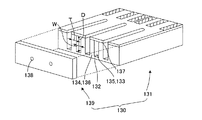
図13は、インクジェットヘッドの一例を示す斜視図である。図示されるインクジェットヘッド130は、ノズル138が形成されたノズル板139によって、アクチュエータ131のインク室135を塞いで構成される。アクチュエータ131のインク室135は、圧電/電歪作動部134が側壁136となって、基板132及び蓋板137とともに形成するセル133により構成され、図示しないインク供給路に連通する。インクジェットヘッド130において、各圧電/電歪作動部134(各側壁136)に駆動電圧が印加され、各インク室135(各セル133)に容積変化が発生することにより、インクがノズル138から吐出して、印字、印刷が行われる。尚、アクチュエータを用いたインクジェットヘッドの参考文献として、例えば特許文献1が挙げられる。
FIG. 13 is a perspective view illustrating an example of an inkjet head. The illustrated
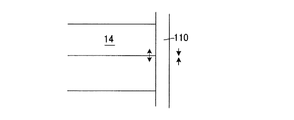
ところで、より鮮明な印刷の実現という印刷機器に対する目標には限りがなく、圧電方式のインクジェットヘッド(アクチュエータ)に対しては、圧電/電歪作動部134(側壁136)及びインク室135(セル133)の配置密度の更なる向上が求められている。現在、インク室135は、少なくとも180dpi(dot per inch)の密度で配置することが要望されている。この場合、ノズル138のピッチは141μm/個(=25.4mm(1インチ)/180個)になるが、このようにノズル138のピッチが小さくなれば、各インク室135(各セル133)の幅W(図13参照)、及び、インク室135を形成する各圧電/電歪作動部134(各側壁136)の厚さT(図13参照)は、ともに小さくなる。他方、インク室135の体積を確保するためには、その幅Wが狭くなる分だけ、その深さD(高さ)を大きくする必要がある(通常、インク室135の深さは圧電/電歪作動部134の高さに等しく一定である)。即ち、圧電/電歪作動部134(側壁136)及びインク室135(セル133)の配置密度を大きくすることは、圧電/電歪作動部4のアスペクト比(=D/T)及びインク室135のアスペクト比(=D/W)が大きくなることを意味する。各インク室135において、その幅Wではなく奥行き(長手方向)を大きくすることによっても体積を確保することは可能であるが、アクチュエータ全体としての実装面積の拡大につながるため、好ましい方法ではない。
By the way, there is no limit to the target for the printing apparatus to realize clearer printing, and for the piezoelectric inkjet head (actuator), the piezoelectric / electrostrictive operation unit 134 (side wall 136) and the ink chamber 135 (cell 133). ) Is required to be further improved. At present, the ink chamber 135 is required to be arranged at a density of at least 180 dpi (dot per inch). In this case, the pitch of the
インクジェットヘッドを構成する上記のような圧電/電歪作動部を備えるアクチュエータは、グリーンシート積層法により形成された積層体を焼成することで作製することが出来る。図14(a)〜図14(c)は、図13に示されるインクジェットヘッド130を構成するアクチュエータ131を製造する工程を示す説明図である。
An actuator including the above-described piezoelectric / electrostrictive operation portion constituting the ink jet head can be manufactured by firing a laminate formed by a green sheet laminating method. FIG. 14A to FIG. 14C are explanatory views showing a process for manufacturing the
先ず、圧電材料にバインダ、溶剤、分散剤、可塑剤等の添加剤を混合して得られるスラリーを用いて、ドクターブレード法等の手法によってグリーンシートを得る。そのグリーンシートに打抜加工等を施して所定形状のグリーンシート16を得て、基板132とともに圧力をかけて積層し、セラミックグリーン積層体143を得る(図14(a)及び図14(b)参照)。得られたセラミックグリーン積層体143を、焼成し、必要に応じ分極処理を施し、必要な配線を行い、蓋板137を取り付ければ、アクチュエータ131を得ることが出来る(図14(c)参照)。尚、電極の形成は、必要に応じ、適宜、行うことが出来る。
しかしながら、このようなグリーンシート積層法により作製されるアクチュエータは、グリーンシートを積層した積層体を焼成したものであるが故に、その積層されたグリーンシートに基づく積層界面を起点として破壊が起こる場合があった。その理由について図2及び図3により説明する。 However, since the actuator produced by such a green sheet lamination method is obtained by firing a laminated body in which green sheets are laminated, destruction may occur starting from a lamination interface based on the laminated green sheets. there were. The reason will be described with reference to FIGS.
図2は、図14(b)に示される焼成前のセラミックグリーン積層体143の部分Aを表す断面図であり、その部分Aは、アクチュエータの圧電/電歪作動部(側壁)及びインク室(セル)に相当する部分である。図3は、図2に示されるセラミックグリーン積層体143の部分Aの更に一部分を拡大した断面図である。グリーンシート積層法における打抜加工の際に、グリーンシート16の端面はテーパー状になり(テーパー状になる理由について特許文献2を参照)、セラミックグリーン積層体143の側面(図2及び図3における垂直面)には、積層されたグリーンシート16に基づく切欠25が発現する。又、図3に示されるように、グリーンシート16の積層ズレも生じ得る(積層ズレが生じる理由について特許文献2を参照)。そうすると、積層されたグリーンシート16を一体化させるべく圧力Pをかけても、切欠25の深さが異なることによってグリーンシート16の積層界面に、密着しない未接合部32が生じてしまう。セラミックグリーン積層体143を焼成して得られるアクチュエータ131において、この未接合部32を起点にクラックが進展し、又、例えば切欠が設けられた側面に一対の電極膜を形成し、この電極膜の間に電圧をかけることによってアクチュエータ131の圧電/電歪作動部が発現する変位に伴う応力負荷も手伝って、破壊に至るのである。特に、グリーンシート16の間に電極層を挟んだ積層体を焼成して得られるアクチュエータの場合には、層間界面がセラミックスと金属とで構成されることになるから、セラミックス同士の界面に比べ、層間の結合力が弱く、より破壊し易くなる。
FIG. 2 is a cross-sectional view showing a portion A of the ceramic
このような問題は、アクチュエータの圧電/電歪作動部(側壁)のアスペクト比が大きくなる(高アスペクト比化する)につれて、ますます顕在化する。その理由は、グリーンシートを積層するための圧力を高くし過ぎると、積層体が座屈してしまうからである。座屈荷重は圧電/電歪作動部の高さの二乗に反比例するから、圧電/電歪作動部が高アスペクト比になると急激に座屈荷重が下がる。従って、積層体を得るべくグリーンシートを一体化させる際の圧力を下げざるを得ない。そうすると、積層ズレの生じていないグリーンシートの開口断面においても未接合部が生まれ易くなる。又、高アスペクト比になって圧電/電歪作動部の幅が狭くなるに従い、未接合部が強度に及ぼす影響は大きくなるから、容易に破壊に至る場合がある。このようなアクチュエータの破壊は、インクジェットヘッドにおいてインク室(セル)からインク漏れが発生することを意味するから、印刷機器の信頼性を著しく貶めることになる。 Such a problem becomes more and more apparent as the aspect ratio of the piezoelectric / electrostrictive operating portion (side wall) of the actuator increases (increases the aspect ratio). The reason is that if the pressure for laminating the green sheets is too high, the laminate will buckle. Since the buckling load is inversely proportional to the square of the height of the piezoelectric / electrostrictive operating portion, the buckling load rapidly decreases when the piezoelectric / electrostrictive operating portion has a high aspect ratio. Therefore, the pressure at the time of integrating the green sheets to obtain a laminate must be reduced. If it does so, it will become easy to produce an unjoined part also in the opening cross section of the green sheet in which lamination gap does not arise. Further, as the aspect ratio becomes higher and the width of the piezoelectric / electrostrictive operation portion becomes narrower, the influence of the unbonded portion on the strength increases, and therefore, it may easily break. Such destruction of the actuator means that ink leakage occurs from the ink chamber (cell) in the ink jet head, so that the reliability of the printing apparatus is remarkably given up.
本発明は、上記した従来技術の抱える課題に鑑みてなされたものであって、その目的とするところは、近時の印刷機器に求められる高解像度の要望に対応すべく、インク室が高密度に配置され、且つ、信頼性の高いインクジェットヘッドを提供可能にすることである。研究が重ねられた結果、グリーンシート積層法によって作製される際に生じる積層界面が露出する側面に、緻密な薄膜を形成し、クラックの起点となる未接合部を埋設して固定し、強度向上を図ることによって、課題を解決し得ることが見出された。より具体的には、以下に示す圧電/電歪構造体をアクチュエータとして適用することにより、上記目的を達成することが可能である。又、本発明は、上記目的が達成可能な圧電/電歪構造体を作製可能な新たな圧電/電歪構造体の製造方法を提供することを、別の目的としている。この目的は、以下に示す圧電/電歪構造体の製造方法により達成される。 The present invention has been made in view of the above-described problems of the prior art, and the object of the present invention is to provide a high-density ink chamber in order to meet the demand for high resolution demanded of recent printing equipment. It is possible to provide a highly reliable inkjet head that is disposed in As a result of repeated research, a dense thin film is formed on the side surface where the lamination interface that occurs when the green sheet is produced by the green sheet lamination method is exposed, and the unbonded part that is the starting point of the crack is buried and fixed to improve strength. It has been found that the problem can be solved by trying. More specifically, the above-described object can be achieved by applying the following piezoelectric / electrostrictive structure as an actuator. Another object of the present invention is to provide a new method for manufacturing a piezoelectric / electrostrictive structure capable of producing a piezoelectric / electrostrictive structure that can achieve the above-described object. This object is achieved by the following method for manufacturing a piezoelectric / electrostrictive structure.
即ち、本発明によれば、複数のシート状の圧電/電歪体が積層されてなる圧電/電歪構造体であって、複数のシート状の圧電/電歪体の積層界面が露出する側面に複数の切欠が形成され、その切欠が現す凹凸面に沿って1層以上の薄膜が形成されている圧電/電歪構造体が提供される(第1の圧電/電歪構造体ともいう)。 That is, according to the present invention, there is provided a piezoelectric / electrostrictive structure formed by laminating a plurality of sheet-like piezoelectric / electrostrictive bodies, and a side surface on which a laminated interface of the plurality of sheet-like piezoelectric / electrostrictive bodies is exposed. A piezoelectric / electrostrictive structure is provided in which a plurality of notches are formed and one or more thin films are formed along the uneven surface where the notches appear (also referred to as a first piezoelectric / electrostrictive structure). .
第1の圧電/電歪構造体において、1層以上の薄膜が、バリア膜、電極膜、絶縁膜、保護膜、防湿膜からなる膜群から選ばれる一の単層膜又は二以上の多層膜で構成されることが好ましい。そして、薄膜の構成要素であるそれぞれの膜は、バリア膜が酸化物又は窒化物で形成され、電極膜が金属又は酸化物で形成され、絶縁膜、保護膜、及び防湿膜が、酸化物、窒化物、又は炭化物で形成されることが好ましい。 In the first piezoelectric / electrostrictive structure, one or more thin films are selected from the group consisting of a barrier film, an electrode film, an insulating film, a protective film, and a moisture-proof film, or two or more multilayer films It is preferable that it is comprised. Each of the thin film components includes a barrier film formed of an oxide or a nitride, an electrode film formed of a metal or an oxide, an insulating film, a protective film, and a moisture-proof film formed of an oxide, It is preferably formed of nitride or carbide.
又、第1の圧電/電歪構造体において、1層以上の薄膜が、バリア膜と電極膜とを含む多層膜であり、圧電/電歪体の表面から、少なくともバリア膜、電極膜の順に成膜されていることが好ましい。 In the first piezoelectric / electrostrictive structure, one or more thin films are multilayer films including a barrier film and an electrode film, and at least the barrier film and the electrode film in this order from the surface of the piezoelectric / electrostrictive body. A film is preferably formed.
次に、本発明によれば、複数のシート状の圧電/電歪体が積層されてなる圧電/電歪構造体であって、複数のシート状の圧電/電歪体の積層界面が露出する側面に複数の切欠が形成され、その切欠が現す凹凸面に沿って1層以上の薄膜が形成され、その1層以上の薄膜が、絶縁膜、保護膜、防湿膜からなる膜群から選ばれる一の単層膜又は二以上の多層膜で構成されるとともに、薄膜の熱膨張率が圧電/電歪体の熱膨張率より小さい圧電/電歪構造体が提供される(第2の圧電/電歪構造体ともいう)。 Next, according to the present invention, there is provided a piezoelectric / electrostrictive structure in which a plurality of sheet-like piezoelectric / electrostrictive bodies are laminated, and a laminated interface of the plurality of sheet-like piezoelectric / electrostrictive bodies is exposed. A plurality of notches are formed on the side surface, and one or more thin films are formed along the uneven surface where the notches appear, and the one or more thin films are selected from a film group consisting of an insulating film, a protective film, and a moisture-proof film. A piezoelectric / electrostrictive structure having a single layer film or two or more multilayer films and having a thermal expansion coefficient of the thin film smaller than that of the piezoelectric / electrostrictive body is provided (second piezoelectric / electrostrictive structure). Also called electrostrictive structure).
第2の圧電/電歪構造体において、絶縁膜、保護膜、及び防湿膜は、酸化物、窒化物、又は炭化物で形成されることが好ましい。 In the second piezoelectric / electrostrictive structure, the insulating film, the protective film, and the moisture-proof film are preferably formed of an oxide, a nitride, or a carbide.
又、第2の圧電/電歪構造体において、圧電/電歪体の熱膨張率を1としたときの薄膜の熱膨張率が0.3乃至0.9であることが好ましい。 In the second piezoelectric / electrostrictive structure, it is preferable that the thermal expansion coefficient of the thin film is 0.3 to 0.9 when the piezoelectric / electrostrictive body has a thermal expansion coefficient of 1.
即ち、好ましい熱膨張率比(圧電/電歪体の熱膨張率に対する薄膜の熱膨張率の比率)が0.3乃至0.9である。熱膨張率比は、より好ましくは0.35乃至0.85であり、更に好ましくは0.4乃至0.8である。尚、第2の圧電/電歪構造体において、薄膜は、絶縁膜、保護膜、防湿膜のうちの何れか一又は二以上の膜を含むから、薄膜の熱膨張率とは、薄膜に含まれる絶縁膜、保護膜、防湿膜の全ての熱膨張率を指し、圧電/電歪体の熱膨張率を1としたときの薄膜の熱膨張率が0.3乃至0.9であるとは、薄膜に含まれる絶縁膜、保護膜、防湿膜の全ての熱膨張率が、この条件を満たすことを意味する。又、圧電/電歪体の熱膨張率とは、圧電/電歪体を構成する圧電/電歪材料の熱膨張率である。 That is, a preferable thermal expansion coefficient ratio (ratio of the thermal expansion coefficient of the thin film to that of the piezoelectric / electrostrictive body) is 0.3 to 0.9. The thermal expansion ratio is more preferably 0.35 to 0.85, and still more preferably 0.4 to 0.8. In the second piezoelectric / electrostrictive structure, since the thin film includes one or more of an insulating film, a protective film, and a moisture-proof film, the thermal expansion coefficient of the thin film is included in the thin film. The thermal expansion coefficient of the thin film when the thermal expansion coefficient of the piezoelectric / electrostrictive body is 1 is 0.3 to 0.9. It means that all the thermal expansion coefficients of the insulating film, the protective film, and the moisture-proof film included in the thin film satisfy this condition. The thermal expansion coefficient of the piezoelectric / electrostrictive body is the thermal expansion coefficient of the piezoelectric / electrostrictive material constituting the piezoelectric / electrostrictive body.
又、第2の圧電/電歪構造体において、1層以上の薄膜が、更に電極膜を含んで構成され、圧電/電歪体の表面から、少なくとも電極膜、絶縁膜の順、少なくとも電極膜、保護膜の順、少なくとも電極膜、防湿膜の順、の何れかによって成膜されていることが好ましい。 Further, in the second piezoelectric / electrostrictive structure, one or more thin films further include an electrode film, and from the surface of the piezoelectric / electrostrictive body, at least an electrode film, an insulating film, and at least an electrode film. The protective film is preferably formed in the order of at least the electrode film and the moisture-proof film.
第2の圧電/電歪構造体においては、薄膜に電極膜が含まれる場合に、1層以上の薄膜が、尚更にバリア膜を含んで構成される多層膜であり、圧電/電歪体の表面から、少なくともバリア膜、電極膜の順に成膜されていることが好ましい。 In the second piezoelectric / electrostrictive structure, when an electrode film is included in the thin film, one or more thin films are multilayer films configured to further include a barrier film. It is preferable that the barrier film and the electrode film are formed in this order from the surface.
第1の圧電/電歪構造体及び第2の圧電/電歪構造体(両方を指すときに単に本発明に係る圧電/電歪構造体ともいう)は、複数のシート状の圧電/電歪体の間に電極層を備える態様を好適に採用出来る。 The first piezoelectric / electrostrictive structure and the second piezoelectric / electrostrictive structure (also simply referred to as the piezoelectric / electrostrictive structure according to the present invention when referring to both) are a plurality of sheet-like piezoelectric / electrostrictive structures. A mode in which an electrode layer is provided between the bodies can be suitably employed.
本発明に係る圧電/電歪構造体において、切欠とは、圧電/電歪構造体自体の一部が切り取られて形成された実体のない開口部分をいう。 In the piezoelectric / electrostrictive structure according to the present invention, the notch refers to a solid opening formed by cutting a part of the piezoelectric / electrostrictive structure itself.
その切欠の具体的形状は限定されるものではないが、より好ましい切欠の断面形状は、概ね三角形である。切欠の断面形状が三角形である場合において、更に好ましくは、切欠の最深部が鋭角に形成されている態様である。切欠の最深部とは、その切欠において圧電/電歪構造体の側面にかかる表平面から最も離れた部分をいう。断面形状とは、圧電/電歪構造体を構成するシート状の圧電/電歪体の面方向に垂直な断面に現される形状である。そのような断面は複数あり得るが、何れかの断面において、概ね三角形として現されれば好ましい形状といえる。尚、圧電/電歪構造体の側面にかかる表平面とは、切欠が設けられていないとした場合の圧電/電歪構造体の側面にかかる表面を指す。 The specific shape of the notch is not limited, but a more preferable cross-sectional shape of the notch is generally a triangle. When the cross-sectional shape of the notch is a triangle, it is more preferable that the deepest part of the notch is formed at an acute angle. The deepest part of the notch refers to a part of the notch that is farthest from the front plane that is applied to the side surface of the piezoelectric / electrostrictive structure. The cross-sectional shape is a shape appearing in a cross section perpendicular to the surface direction of the sheet-like piezoelectric / electrostrictive body constituting the piezoelectric / electrostrictive structure. There can be a plurality of such cross-sections, but if any of the cross-sections is expressed as a generally triangular shape, it can be said to be a preferable shape. Note that the surface plane applied to the side surface of the piezoelectric / electrostrictive structure refers to the surface applied to the side surface of the piezoelectric / electrostrictive structure when notches are not provided.
又、切欠の開口幅が、300μm以下であることが好ましい。切欠の開口幅の下限は限定されるものではないが、精度よく形成するためには、5μm以上の開口幅を必要とする。 Moreover, it is preferable that the opening width of a notch is 300 micrometers or less. The lower limit of the opening width of the notch is not limited, but an opening width of 5 μm or more is required for accurate formation.
更に、切欠の深さが、3乃至50μmであることが好ましい。 Furthermore, the depth of the notch is preferably 3 to 50 μm.
切欠の開口幅とは、圧電/電歪構造体の側面に形成された切欠の開口の輪郭線に内接する円の直径をいう。切欠の深さとは、圧電/電歪構造体の側面にかかる表平面から、最深部まで、即ち、その切欠において圧電/電歪構造体の側面にかかる表平面から最も離れた部分まで、の長さをいう。 The opening width of the notch refers to the diameter of a circle inscribed in the outline of the notch opening formed on the side surface of the piezoelectric / electrostrictive structure. The depth of the notch is the length from the surface plane on the side surface of the piezoelectric / electrostrictive structure to the deepest part, that is, the portion farthest from the surface plane on the side surface of the piezoelectric / electrostrictive structure at the notch. Say it.
本発明に係る圧電/電歪構造体において、切欠とは、意図的に設けられたものであって、製造上の欠陥等により偶発的に存在するものではない。切欠は、限定されるものではないが、圧電/電歪構造体における複数のシート状の圧電/電歪体の積層界面が露出する全ての側面に形成されていることが好ましい。 In the piezoelectric / electrostrictive structure according to the present invention, the notch is intentionally provided and does not exist accidentally due to a manufacturing defect or the like. The notches are not limited, but are preferably formed on all the side surfaces of the piezoelectric / electrostrictive structure body where a plurality of sheet-like piezoelectric / electrostrictive layer stack interfaces are exposed.
本発明に係る圧電/電歪構造体において、切欠が現す凹凸面に沿って1層以上の薄膜が形成されている、とは、切欠が形成される結果として、複数のシート状の圧電/電歪体が積層されてなる圧電/電歪構造体において、その複数のシート状の圧電/電歪体の積層界面が露出する側面が凹凸面となり、その凹凸状態が表されたままに、即ち、塗布されて出来た膜の如く凹凸を埋めて平坦にならずに、薄い膜が形成されている、ことを意味する。 In the piezoelectric / electrostrictive structure according to the present invention, one or more thin films are formed along the uneven surface where the notches appear. As a result of the notches being formed, a plurality of sheet-like piezoelectric / electrostrictive structures are formed. In the piezoelectric / electrostrictive structure in which the strain bodies are laminated, the side surface where the laminated interface of the plurality of sheet-like piezoelectric / electrostrictive bodies is exposed becomes an uneven surface, and the uneven state is expressed. It means that a thin film is formed without filling the unevenness and flattening like a film formed by coating.
本発明に係る圧電/電歪構造体は、そのアスペクト比が、5乃至100であることが好ましい。より好ましいアスペクト比は7乃至100であり、更に好ましくは10乃至100である。尚、圧電/電歪構造体のアスペクト比とは、高さと短手方向の幅との比を指し、高さ/短手方向の幅、で示される。 The piezoelectric / electrostrictive structure according to the present invention preferably has an aspect ratio of 5 to 100. A more preferred aspect ratio is 7 to 100, and even more preferred is 10 to 100. The aspect ratio of the piezoelectric / electrostrictive structure refers to the ratio between the height and the width in the short direction, and is indicated by the height / width in the short direction.
次に、本発明によれば、2つの側壁と、その2つの側壁を接続する蓋板及び底板と、によって形成されたセルが複数備わり、少なくとも2つの側壁が、上記した何れかの圧電/電歪構造体で構成され、その圧電/電歪構造体の変位によってセルの容積が変化するセル駆動型圧電/電歪アクチュエータが提供される。このセル駆動型圧電/電歪アクチュエータでは、特に、2つの側壁が上記した好ましいアスペクト比の条件に適う薄く背の高い圧電/電歪構造体で構成されることが望ましい。このセル駆動型圧電/電歪アクチュエータをインクジェットヘッドとして適用すると、2つの側壁が圧電/電歪作動部に相当し、それが形成するセルがインク室に相当し、圧電/電歪作動部及びインク室の高密度化が図れ、より鮮明な印刷の実現が望まれる近時の印刷機器用のインクジェットヘッドとして好適なものになる。 Next, according to the present invention, there are provided a plurality of cells formed by two side walls, a lid plate and a bottom plate connecting the two side walls, and at least two side walls have any one of the piezoelectric / electrical devices described above. There is provided a cell driving type piezoelectric / electrostrictive actuator which is composed of a strained structure and whose cell volume is changed by displacement of the piezoelectric / electrostrictive structure. In this cell drive type piezoelectric / electrostrictive actuator, it is particularly desirable that the two side walls are composed of a thin and tall piezoelectric / electrostrictive structure that meets the above-mentioned preferred aspect ratio conditions. When this cell driving type piezoelectric / electrostrictive actuator is applied as an ink jet head, two side walls correspond to piezoelectric / electrostrictive operating portions, and the cells formed by them correspond to ink chambers. It is possible to increase the density of the chamber, and it is suitable as an ink jet head for a recent printing apparatus in which a clearer printing is desired.
次に、本発明によれば、圧電/電歪材料からなる複数のセラミックグリーンシートを積層し焼成して、圧電/電歪焼成体を得る工程と、得られた圧電/電歪焼成体の、複数のセラミックグリーンシートに基づく積層界面が露出する側面に、CVD成膜法によって、1層以上の薄膜を形成して圧電/電歪構造体を得る工程と、を有する圧電/電歪構造体の製造方法が提供される。尚、本明細書において、セラミックグリーンシートを、単にグリーンシートともいう。 Next, according to the present invention, a plurality of ceramic green sheets made of a piezoelectric / electrostrictive material are stacked and fired to obtain a piezoelectric / electrostrictive fired body, and the obtained piezoelectric / electrostrictive fired body, Forming a piezoelectric / electrostrictive structure by forming one or more thin films on a side surface where a laminated interface based on a plurality of ceramic green sheets is exposed by a CVD film forming method. A manufacturing method is provided. In the present specification, the ceramic green sheet is also simply referred to as a green sheet.
本発明に係る圧電/電歪構造体の製造方法においては、薄膜の成膜温度が、150乃至850℃であることが好ましい。成膜温度は、より好ましくは180乃至800℃であり、更に好ましくは200乃至750℃である。 In the method for manufacturing a piezoelectric / electrostrictive structure according to the present invention, the film forming temperature of the thin film is preferably 150 to 850 ° C. The film forming temperature is more preferably 180 to 800 ° C., and further preferably 200 to 750 ° C.
又、薄膜の成膜圧力が、0.1乃至20000Paであることが好ましい。成膜圧力は、より好ましくは0.2乃至18000Paであり、更に好ましくは0.3乃至15000Paである。 Further, the film forming pressure of the thin film is preferably 0.1 to 20000 Pa. The film forming pressure is more preferably 0.2 to 18000 Pa, and further preferably 0.3 to 15000 Pa.
本発明に係る圧電/電歪構造体の製造方法において、1層以上の薄膜が、絶縁膜、保護膜、防湿膜からなる膜群から選ばれる一の単層膜又は二以上の多層膜で構成され、CVD成膜法にかかるCVD材料として、アルコキシド系有機金属化合物、乃至、β−ジケトン系有機金属化合物を使用することが好ましい。 In the method for manufacturing a piezoelectric / electrostrictive structure according to the present invention, one or more thin films are composed of one single-layer film or two or more multilayer films selected from a film group consisting of an insulating film, a protective film, and a moisture-proof film. In addition, it is preferable to use an alkoxide-based organometallic compound or a β-diketone-based organometallic compound as a CVD material according to the CVD film forming method.
本発明に係る圧電/電歪構造体の製造方法において、1層以上の薄膜が、バリア膜、電極膜、絶縁膜、保護膜、防湿膜からなる膜群から選ばれる一の単層膜又は二以上の多層膜で構成されることが好ましい。 In the method for manufacturing a piezoelectric / electrostrictive structure according to the present invention, one or more thin films of one or more layers are selected from a film group consisting of a barrier film, an electrode film, an insulating film, a protective film, and a moisture-proof film. It is preferable to be composed of the above multilayer film.
尚、本明細書において、圧電/電歪と表現しているが、電界によって誘起される歪みを利用し得る構造体であって、狭義の意味での、印加電界に概ね比例した歪み量を発生する圧電効果(縦効果、横効果)及び印加電界の二乗に概ね比例した歪み量を発生する電歪効果を利用するものに限定されるものではなく、強誘電体材料全般にみられる分極反転、反強誘電体材料にみられる反強誘電相−強誘電相転移、等の現象を利用し得るものも含まれる。分極にかかる処理が行われるか否かについては、本発明に係る圧電/電歪構造体を構成する圧電/電歪材料の性質に基づいて適宜決定される。 In this specification, although expressed as piezoelectric / electrostrictive, it is a structure that can utilize strain induced by an electric field, and in a narrow sense, generates a strain amount that is roughly proportional to the applied electric field. It is not limited to the piezoelectric effect (vertical effect, lateral effect) and the electrostrictive effect that generates the amount of strain approximately proportional to the square of the applied electric field, but the polarization inversion found in all ferroelectric materials, Those that can utilize the phenomenon such as antiferroelectric phase-ferroelectric phase transition found in antiferroelectric materials are also included. Whether or not the treatment for polarization is performed is appropriately determined based on the properties of the piezoelectric / electrostrictive material constituting the piezoelectric / electrostrictive structure according to the present invention.
又、本明細書において、圧電/電歪体とは、主に圧電/電歪材料からなる定形体であって、焼成されたものを指す。本発明においては、圧電/電歪構造体を構成する圧電/電歪体はシート状である。このシート状の圧電/電歪体の積層数は、複数であればよく限定されない。高変位且つ低駆動電圧の特性を有する高性能なアクチュエータとして適用するためには、シート状の圧電/電歪体はより薄く、その積層数は、より多いことが好ましい。 Further, in this specification, the piezoelectric / electrostrictive body refers to a fixed body mainly made of a piezoelectric / electrostrictive material and fired. In the present invention, the piezoelectric / electrostrictive body constituting the piezoelectric / electrostrictive structure is in the form of a sheet. The number of laminations of the sheet-like piezoelectric / electrostrictive body is not limited as long as it is plural. In order to be applied as a high-performance actuator having high displacement and low drive voltage characteristics, it is preferable that the sheet-like piezoelectric / electrostrictive body is thinner and the number of laminated layers is larger.
更に、図面において、積層体が焼成積層体(圧電/電歪焼成体)であるかセラミックグリーン積層体(グリーンシートの積層体)であるかを問わずに、積層界面を実線で表す場合があるが、これは説明の便宜上示すものであって、焼成後の焼成積層体においては、同種材料であるグリーンシートは一体化されているため、焼成前には存在したシート間の界面は実際には存在しない。 Furthermore, in the drawings, the laminated interface may be represented by a solid line regardless of whether the laminated body is a fired laminated body (piezoelectric / electrostrictive fired body) or a ceramic green laminated body (green sheet laminated body). However, this is shown for convenience of explanation, and in the fired laminate after firing, the green sheet, which is the same material, is integrated, so the interface between the sheets that existed before firing is actually not exist.
本発明に係る(第1及び第2の)圧電/電歪構造体は、複数のシート状の圧電/電歪体の積層界面が露出する側面に薄膜が形成されているので、構造体としての強度が向上しており、例え積層ズレ等によって、複数のシート状の圧電/電歪体の積層界面に、未接合部が生じても、クラックの起点となり難く、長期間の信頼性に優れたものになる。 In the (first and second) piezoelectric / electrostrictive structures according to the present invention, a thin film is formed on the side surface where the laminated interface of a plurality of sheet-like piezoelectric / electrostrictive bodies is exposed. Strength has been improved, and even if unbonded parts occur at the laminated interface of a plurality of sheet-like piezoelectric / electrostrictive bodies due to laminating misalignment, etc., it is difficult to become a starting point of cracks and has excellent long-term reliability. Become a thing.
又、複数のシート状の圧電/電歪体の積層界面が露出する側面に、複数の切欠が形成されているので、焼成にかかる残留応力が抑制され、更に、薄膜が、塗布法によって形成される膜の如く、その切欠が現す凹凸面の凹凸を平面化するような厚い膜ではなく、凹凸を表しつつ、その切欠が現す凹凸面に沿って形成された薄い膜であるため、複数のシート状の圧電/電歪体の積層界面にはたらく応力が小さくなり、クラック自体の発生が抑制され、ますます長期間の信頼性が向上する。 In addition, since a plurality of notches are formed on the side surface where the laminated interface of a plurality of sheet-like piezoelectric / electrostrictive bodies is exposed, residual stress on firing is suppressed, and a thin film is formed by a coating method. It is not a thick film that flattens the unevenness of the uneven surface where the notch appears, but a thin film that is formed along the uneven surface where the notch appears while representing the unevenness. The stress acting on the piezoelectric / electrostrictive laminate interface is reduced, the generation of cracks is suppressed, and the long-term reliability is improved.
そして、このことは、本発明に係る圧電/電歪構造体が、グリーンシートの間に電極層を挟んで焼成一体化したものである場合、即ち、シート状の圧電/電歪体の間に電極層を備える態様である場合において、特に、効果的である。一般的には、このような態様は層間界面がセラミックス(圧電/電歪材料)と金属(材料)とで構成されるから、セラミックス同士の積層に比べ、層間の結合力が弱く、より破壊され易い。しかし、本発明に係る圧電/電歪構造体によれば、側面に薄膜が形成されることで、破壊が抑制される。 And this is the case where the piezoelectric / electrostrictive structure according to the present invention is integrally fired with an electrode layer sandwiched between green sheets, that is, between the sheet-like piezoelectric / electrostrictive bodies. This is particularly effective in the case where the electrode layer is provided. In general, in such an embodiment, the interlayer interface is composed of ceramics (piezoelectric / electrostrictive material) and metal (material), so the bonding force between the layers is weaker than that of ceramics, and the layer is more destroyed. easy. However, according to the piezoelectric / electrostrictive structure according to the present invention, the thin film is formed on the side surface, so that the breakage is suppressed.
本発明に係る圧電/電歪構造体は、限定されるものではないが、本発明に係る圧電/電歪構造体の製造方法によって作製することが好ましい。本発明に係る圧電/電歪構造体の製造方法によれば、グリーンシート積層法によって、複数のシート状の圧電/電歪体の積層界面が露出する全ての側面に切欠が形成され、CVD成膜法によって、外部に露出する複数のシート状の圧電/電歪体の積層界面に、緻密な薄膜が形成される。従って、積層界面が確実に保護され、構造体として充分な強度を有するものになる。又、薄膜が極薄いから、切欠が作り出す凹凸面の凹凸を埋めて平面化することなく、積層界面への応力緩衝作用を発現し、上記本発明に係る圧電/電歪構造体が導く効果を充分に享受出来るものになる。 The piezoelectric / electrostrictive structure according to the present invention is not limited, but is preferably produced by the method for manufacturing a piezoelectric / electrostrictive structure according to the present invention. According to the method for manufacturing a piezoelectric / electrostrictive structure according to the present invention, a notch is formed on all side surfaces where the lamination interface of a plurality of sheet-like piezoelectric / electrostrictive bodies is exposed by a green sheet laminating method. By the film method, a dense thin film is formed at the laminated interface of the plurality of sheet-like piezoelectric / electrostrictive bodies exposed to the outside. Accordingly, the laminated interface is surely protected and has a sufficient strength as a structure. In addition, since the thin film is extremely thin, the stress buffering action to the laminated interface is expressed without filling the unevenness of the uneven surface created by the notch and planarizing, and the piezoelectric / electrostrictive structure according to the present invention leads to the effect. It will be something you can fully enjoy.
本発明に係る圧電/電歪構造体は、電極膜を設ける場合には、好ましくは、圧電/電歪体の表面上に、更に拡散防止用のバリア膜が設けられる。こうすると、電極膜を形成した後に絶縁膜、保護膜、防湿膜の何れか一の単層膜又は二以上の多層膜を形成しても、電極膜の成分が圧電/電歪体の中へ拡散したり、逆に圧電/電歪体の成分が電極膜へ拡散することにより圧電/電歪特性を劣化させるおそれがない。 In the piezoelectric / electrostrictive structure according to the present invention, when an electrode film is provided, it is preferable that a barrier film for preventing diffusion is further provided on the surface of the piezoelectric / electrostrictive body. In this way, even if an insulating film, a protective film, a moisture-proof film, or a single-layer film or two or more multilayer films are formed after the electrode film is formed, the components of the electrode film enter the piezoelectric / electrostrictive body. There is no possibility that the piezoelectric / electrostrictive characteristics are deteriorated by diffusion or conversely, components of the piezoelectric / electrostrictive body diffuse into the electrode film.
本発明に係る第2の圧電/電歪構造体は、絶縁膜、保護膜、防湿膜のうち一の単層膜又は二以上の多層膜で構成される1層以上の薄膜の熱膨張率が、圧電/電歪体の熱膨張率より小さいため、成膜の後において、薄膜と圧電/電歪体との間の熱膨張率差に起因する残留応力として、薄膜には圧縮応力が残留し、圧電/電歪体(圧電/電歪構造体)には引張応力が残留する傾向になる。一般に、セラミックス(圧電/電歪材料)は、引張応力に弱く、圧縮応力に強い性質を有するため、薄膜にかかる応力を圧縮応力とすることによって、薄膜自体が破壊され難い安定したものになる。 The second piezoelectric / electrostrictive structure according to the present invention has a thermal expansion coefficient of one or more thin films composed of one single-layer film or two or more multilayer films among an insulating film, a protective film, and a moisture-proof film. Since the thermal expansion coefficient is smaller than that of the piezoelectric / electrostrictive body, compressive stress remains in the thin film as residual stress due to the difference in thermal expansion coefficient between the thin film and the piezoelectric / electrostrictive body after film formation. The tensile stress tends to remain in the piezoelectric / electrostrictive body (piezoelectric / electrostrictive structure). In general, ceramics (piezoelectric / electrostrictive materials) are weak against tensile stress and strong against compressive stress. Therefore, by using a stress applied to the thin film as a compressive stress, the thin film itself is not easily destroyed.
他方、引張応力がかかる圧電/電歪体においても、応力がかかる方向を微視的にみると、複数のシート状の圧電/電歪体が積層された圧電/電歪構造体としての側面に切欠を有することから、引張応力は、複数のシート状の圧電/電歪体による積層界面の方向に対し、垂直方向にかからずに、応力緩衝作用がはたらく。従って、圧電/電歪構造体としての耐久性も向上し、好適である。又、アクチュエータ等に応用された際に、薄膜が極薄いものであるので変位に対する拘束力が極小さく、変位発生部(圧電/電歪作動部)になる圧電/電歪構造体が、容易に変位を発生し易く、少なくとも変位を妨げる応力を最小限のものとすることになるので、大きなインク吐出力を所望されるインクジェットヘッド等として好適である。 On the other hand, even in a piezoelectric / electrostrictive body to which tensile stress is applied, when the direction in which the stress is applied is viewed microscopically, the side surface as a piezoelectric / electrostrictive structure in which a plurality of sheet-like piezoelectric / electrostrictive bodies are stacked is provided. Since it has a notch, the tensile stress acts in a stress buffering manner without being perpendicular to the direction of the laminated interface formed by a plurality of sheet-like piezoelectric / electrostrictive bodies. Therefore, durability as a piezoelectric / electrostrictive structure is improved, which is preferable. In addition, when applied to an actuator or the like, since the thin film is extremely thin, the restraining force against displacement is extremely small, and a piezoelectric / electrostrictive structure that becomes a displacement generating part (piezoelectric / electrostrictive operating part) can be easily obtained. Since it is easy to generate a displacement and at least a stress that prevents the displacement is minimized, it is suitable for an inkjet head or the like that requires a large ink ejection force.
本発明に係る圧電/電歪構造体は、以上の効果を有するものであるから、信頼性を保持し又は向上させた上で、そのアスペクト比をより大きくすることが可能である。即ち、アスペクト比を大きくすると、座屈荷重が小さくなり圧電/電歪構造体を得る際に大きな圧力をかけられないが、そうであっても、構造体の強度は、より高く保持され、破壊され難い。 Since the piezoelectric / electrostrictive structure according to the present invention has the above effects, it is possible to increase the aspect ratio while maintaining or improving the reliability. That is, when the aspect ratio is increased, the buckling load is reduced and a large pressure cannot be applied to obtain the piezoelectric / electrostrictive structure. However, the strength of the structure is maintained higher and the fracture is not caused. It is hard to be done.
本発明に係る圧電/電歪構造体であって高アスペクト比のものを、インクジェットヘッドを構成するアクチュエータの側壁(圧電/電歪作動部)として適用することにより、信頼性が高く高解像度を実現し得るインクジェットヘッドの提供が可能となる。インクジェットヘッドにおいて、圧電/電歪作動部(側壁)を高アスペクト比にすると、その間のインク室(セル)の体積を確保しつつ、実装面積を拡大することなく圧電/電歪作動部及びインク室の配置密度を向上出来るからである。 By applying the piezoelectric / electrostrictive structure according to the present invention having a high aspect ratio as the side wall (piezoelectric / electrostrictive actuating portion) of the actuator constituting the inkjet head, high reliability and high resolution can be realized. It is possible to provide an inkjet head that can be used. In the ink jet head, when the piezoelectric / electrostrictive operating portion (side wall) has a high aspect ratio, the piezoelectric / electrostrictive operating portion and the ink chamber are secured without enlarging the mounting area while securing the volume of the ink chamber (cell) therebetween. This is because the arrangement density can be improved.
又、高アスペクト比な圧電/電歪構造体は、一定の駆動電圧で、より大きな変位が得られるので、本発明に係る圧電/電歪構造体であって高アスペクト比のものを、DNAチップ製造装置等における液体吐出機構を構成するアクチュエータの圧電/電歪作動部として適用することにより、セル(液体室)の体積変動を大きくすることが出来、液体吐出量をより多くすることが可能である。このことは、換言すれば、変位量(吐出量)を同じとすれば、より低い(小さい)電圧で駆動出来ることを意味するから、本発明に係る圧電/電歪構造体の採用により、より省エネルギーな液体吐出機構が実現される。更に、高アスペクト比な圧電/電歪構造体は、変位と発生力を両立する上でも有利であり、大きな発生力で体積変動を大きく出来るため、高粘度な液体も確実に吐出することが可能である。 In addition, since the piezoelectric / electrostrictive structure having a high aspect ratio can obtain a larger displacement at a constant driving voltage, the piezoelectric / electrostrictive structure according to the present invention having a high aspect ratio can be used as a DNA chip. By applying it as a piezoelectric / electrostrictive actuating part of an actuator that constitutes a liquid ejection mechanism in a manufacturing apparatus or the like, it is possible to increase the volume fluctuation of the cell (liquid chamber) and to increase the liquid ejection amount. is there. In other words, this means that if the amount of displacement (discharge amount) is the same, it can be driven with a lower (smaller) voltage. Therefore, by adopting the piezoelectric / electrostrictive structure according to the present invention, An energy-saving liquid discharge mechanism is realized. Furthermore, a piezoelectric / electrostrictive structure with a high aspect ratio is advantageous for achieving both displacement and generated force, and the volume fluctuation can be increased with a large generated force, so that highly viscous liquids can be discharged reliably. It is.
以下、本発明の圧電/電歪構造体及び圧電/電歪構造体の製造方法について、適宜、図面を参酌しながら、実施の形態を説明するが、本発明はこれらに限定されて解釈されるべきものではない。本発明の要旨を損なわない範囲で、当業者の知識に基づいて、種々の変更、修正、改良、置換を加え得るものである。例えば、図面は、好適な本発明の実施の形態を表すものであるが、本発明は図面に表される態様や図面に示される情報により制限されない。本発明を実施し又は検証する上では、本明細書中に記述されたものと同様の手段若しくは均等な手段が適用され得るが、好適な手段は、以下に記述される手段である。 Hereinafter, embodiments of the piezoelectric / electrostrictive structure and the method for manufacturing the piezoelectric / electrostrictive structure of the present invention will be described with reference to the drawings as appropriate. However, the present invention is interpreted as being limited thereto. It shouldn't be. Various changes, modifications, improvements, and substitutions can be added based on the knowledge of those skilled in the art without departing from the scope of the present invention. For example, the drawings show preferred embodiments of the present invention, but the present invention is not limited by the modes shown in the drawings or the information shown in the drawings. In practicing or verifying the present invention, the same means as described in this specification or equivalent means can be applied, but preferred means are those described below.
先ず、本発明に係る圧電/電歪構造体について説明する。図1(a)は、本発明に係る圧電/電歪構造体の一実施形態を示す図であり、それを構成要素として含むインクジェットヘッドを表す斜視図である。又、図1(b)は、図1(a)に示されるインクジェットヘッド1を切断線100で切断した場合の断面図である。図1(a)、図1(b)に示されるインクジェットヘッド1は、アクチュエータ11と、ノズル8が開いたノズル板9とで構成され、本発明に係る圧電/電歪構造体は、アクチュエータ11として適用されている。尚、インクジェットヘッド1は、ノズル板9とアクチュエータ11とを一体的なものとして作製することも可能である。
First, the piezoelectric / electrostrictive structure according to the present invention will be described. FIG. 1A is a diagram showing an embodiment of a piezoelectric / electrostrictive structure according to the present invention, and is a perspective view showing an ink jet head including the same as a component. FIG. 1B is a cross-sectional view of the
アクチュエータ11は、2つの側壁6と、その2つの側壁6を接続するノズル板9(蓋板に相当する)及び底板2と、によって形成された概ね直方体形状をなすセル3を複数備えるものである。2つの側壁6は、本発明に係る圧電/電歪構造体により、圧電/電歪作動部4として構成され、その圧電/電歪作動部4(圧電/電歪構造体)の変位によって、セル3の容積が変化する。尚、複数のセル3の間の空間は、ダミーセル15として構成される。インクジェットヘッド1では、セル3はインク室5(液体加圧室)として用いられ、圧電/電歪作動部4(側壁6)が上下方向に伸縮しセル3の容積を変化させ、セル3に充填された液体を送出させることが出来る。
The
本発明に係る圧電/電歪構造体は、複数のシート状の圧電/電歪体が積層された構造体であるが、種々の態様があり、例えば、シート状の圧電/電歪体の積層態様、あるいは変位を生じる圧電/電歪作動部として機能させるべく電界をかけるための電極の形成態様、等によって分類することが出来る。以下、インクジェットヘッド1のアクチュエータ11として適用可能な圧電/電歪構造体を例示して説明する。
The piezoelectric / electrostrictive structure according to the present invention is a structure in which a plurality of sheet-like piezoelectric / electrostrictive bodies are laminated, and there are various modes, for example, a lamination of sheet-like piezoelectric / electrostrictive bodies. It can be classified according to the form, or the form of the electrode for applying an electric field so as to function as a piezoelectric / electrostrictive actuating part that generates displacement. Hereinafter, a piezoelectric / electrostrictive structure applicable as the
(1)縦積み型
複数のシート状の圧電/電歪体が縦方向に積層されたタイプの圧電/電歪構造体である。積層方向である縦方向とは、別言すれば、構成要素である圧電/電歪作動部の高さ方向に相当する方向である。
(1) Vertical stacking type A piezoelectric / electrostrictive structure in which a plurality of sheet-like piezoelectric / electrostrictive bodies are stacked in the vertical direction. In other words, the longitudinal direction, which is the stacking direction, is a direction corresponding to the height direction of the piezoelectric / electrostrictive operation unit that is a component.
図5(a)は、縦積み型の圧電/電歪構造体の一実施形態を示す図であり、図1(b)と同様の断面図であり、セル周辺を拡大し、側壁等に薄膜が形成されている様子を表した図である。図5(b)は、図5(a)に示される圧電/電歪構造体の、複数のシート状の圧電/電歪体の積層界面が露出する側面近傍の部分拡大図である。圧電/電歪構造体51は、側壁6を構成する圧電/電歪作動部4が、複数の圧電/電歪体14と電極層18,19とが交互に縦方向に積層されてなり、1つおきのセル3を形成する側壁6に共通電極として電極膜28,1つおきのダミーセル15を形成する側壁6に個別電極として電極膜29が形成されている。電極層18,19の端部は、それぞれ一方において圧電/電歪体14内に埋設され、他方において圧電/電歪体14から露出し、電極層18は電極膜28と接続され、電極層19は電極膜29と接続される。セル3に対面する電極膜28の上には保護膜17が形成され、ダミーセル15に対面する電極膜29の上には絶縁膜177が形成される。保護膜17は、例えばセル3に腐食性液体が充填される場合には、電極膜28を保護するための膜としてのはたらき、絶縁膜177は、電極膜29を絶縁する膜としてはたらく。尚、これら保護膜と絶縁膜は、両者の効果が得られる材料を選択して、何れもが同一の単層膜とすることが望ましい。
FIG. 5A is a view showing an embodiment of a vertically stacked piezoelectric / electrostrictive structure, and is a cross-sectional view similar to FIG. 1B, in which the periphery of the cell is enlarged and a thin film is formed on the side wall or the like. It is a figure showing a mode that is formed. FIG. 5B is a partially enlarged view of the piezoelectric / electrostrictive structure shown in FIG. 5A in the vicinity of a side surface where a plurality of sheet-like piezoelectric / electrostrictive laminate interfaces are exposed. The piezoelectric /
尚、電極膜28,29は圧電/電歪体14の中に設けることが可能であり、その場合には、例えばセル3に腐食性液体が充填される場合に、保護膜17は電極膜18を保護するための膜としてはたらき、絶縁膜177は、電極膜19を絶縁するための膜としてはたらく。電極膜28,29及び上記のような膜で構成される保護膜17、絶縁膜177が形成される場合には、側壁6には電極膜28,29より先に(下面に)バリア膜が形成されてもよい(図示しない)。
The
圧電/電歪構造体51は、図5(b)に示されるように(図5(a)では表現を省いている)、複数の圧電/電歪体14の積層界面が露出しセル3に対面する側の側面に、複数の切欠25が形成され、その切欠25が現す凹凸面に沿って、図5(b)に示される切欠25の断面形状そのままに、電極膜28及び保護膜17が形成されている。電極膜28及び保護膜17は、切欠25の深さに比較して相対的に薄く、切欠25を埋めて側壁6の表面を平面にすることがなく、本発明に係る圧電/電歪構造体の特徴を表している。図示しないが、ダミーセル15に対面する側の側面でも、同様に切欠25が形成され、同様に切欠25が現す凹凸面に沿って電極膜29及び絶縁膜177が形成されている。
In the piezoelectric /
尚、切欠の深さ及び開口幅について図15を参照して説明する。図15は、電極層及び薄膜を省いた圧電/電歪構造体の断面を示す図である。図15に示されるように、切欠の開口幅Aは、シート状の圧電/電歪体14の高さに相当する。又、切欠の深さBは、圧電/電歪構造体51の表平面150から切欠の最深部Pまでの長さになる。
The depth and opening width of the notch will be described with reference to FIG. FIG. 15 is a view showing a cross section of the piezoelectric / electrostrictive structure without the electrode layer and the thin film. As shown in FIG. 15, the opening width A of the notch corresponds to the height of the sheet-like piezoelectric /
ここで、切欠が形成されていることに基づく効果を、図11(a)及び図11(b)を参照して説明する。図11(a)は、図5(b)と同様に、圧電/電歪構造体における複数のシート状の圧電/電歪体14の積層界面が露出する側面の部分拡大図であり、その側面に複数の切欠25が形成され、保護膜等の薄膜110が成膜されている様子が示されている。図11(b)は、切欠が形成されていないとした場合の同側面の部分拡大図である。図11(b)は、例えばダイシング等の機械加工により圧電/電歪構造体を作製した場合にみられる形態である。
Here, the effect based on the formation of the notch will be described with reference to FIGS. 11 (a) and 11 (b). FIG. 11A is a partially enlarged view of the side surface of the piezoelectric / electrostrictive structure body where the laminated interface of the plurality of sheet-like piezoelectric /
例えば、焼成して得られる圧電/電歪構造体において、シート状の圧電/電歪体14の熱膨張率より薄膜110の熱膨張率が小さい場合には、このように切欠25が形成されていると、圧電/電歪構造体側にかかる残留応力は、図11(a)中の矢印で示される方向にはたらくから、複数のシート状の圧電/電歪体14の積層界面に対して一定の角度をもった力となり、より弱いものになる。即ち、積層界面近傍でのクラックの発生が抑制される。一方、切欠が形成されていない側面が平面である場合には、圧電/電歪構造体側にかかる残留応力は、図11(b)中の矢印で示される方向にはたらき、複数のシート状の圧電/電歪体の積層界面に対して、より直接的にはたらくから、より積層界面近傍においてクラックが発生し易くなる。
For example, in the piezoelectric / electrostrictive structure obtained by firing, when the thermal expansion coefficient of the
図5(a)、図5(b)に示される圧電/電歪構造体51は、側壁6を構成する圧電/電歪作動部4毎に圧電/電歪体14を8層有している。本発明に係る圧電/電歪構造体では、シート状の圧電/電歪体の積層数は、用途、目的によって適宜決められることとなるが、製造容易性を考慮し、好ましいシート状の圧電/電歪体の積層数は2乃至300程度である。
A piezoelectric /
圧電/電歪構造体51において、シート状の圧電/電歪体14は、例えば電極層18から電極層19へ向けた方向(図5(a)中において上下方向)に分極されている(挟まれる電極層により各圧電/電歪体14毎に分極方向が異なる)。そして、電極膜28,29を介して、電極層18側を正、電極層19側を負にして電極層18,19間に電圧を印加することにより、先に記した分極方向と同じ方向の電界が形成される。換言すれば、圧電/電歪構造体51は、分極が互いに反対方向の圧電/電歪体14が電極層18,19を挟んで積層されてなり、各々の圧電/電歪体14においては、分極と駆動電界とが同一方向になっている。その結果、圧電/電歪体14には電界誘起歪みが発現し、その縦効果による変位に基づき、圧電/電歪作動部4は、圧電/電歪体14が電極層18,19で挟まれる部分においては図5(a)中において概ね上下方向に(底板2に対し垂直に)伸縮しようとする。この圧電/電歪体14の変位は、電界誘起歪みを直接利用しているので、発生力が大きく応答速度も速い。個々の圧電/電歪体14が発現する変位量は大きなものではないが、積層数に比例した変位量となるので、積層数を増やすことによって大変位を得ることが可能である。
In the piezoelectric /
一方、圧電/電歪構造体51においては、圧電/電歪体14の1層当たりの厚さを、好ましくは100μm以下、より好ましくは10乃至80μmとすることによって、より低電圧で駆動出来るようにすることも可能である。
On the other hand, the piezoelectric /
又、圧電/電歪構造体のアスペクト比は、変位発生部分毎に求められ、圧電/電歪構造体51では、1つの圧電/電歪作動部4(変位発生部分)を構成する側壁の高さと幅との比(高さ/幅)になる。図5(a)の圧電/電歪構造体51は、図1(b)のアクチュエータ11に相当するから、図5(a)は圧電/電歪構造体51の短手方向の断面を示す図であり、圧電/電歪構造体のアスペクト比は、図5(a)に表現された1つの圧電/電歪作動部4(側壁6)の縦と横の比(縦/横)で示される。尚、図5(a)においては圧電/電歪構造体51がアスペクト比が3程度で表現されているが、本発明に係る圧電/電歪構造体において、より好ましいアスペクト比は5乃至100である。例えば、図1(b)に示されるアクチュエータ11において、側壁6(圧電/電歪作動部4)は、その厚さTと高さ(セルの深さDに相当)で表されるアスペクト比(=D/T)が15程度である。セルの幅Wとセルの深さD(側壁の高さに相当)で示されるセルのアスペクト比(=D/W)は5程度である。
Further, the aspect ratio of the piezoelectric / electrostrictive structure is obtained for each displacement generating portion. In the piezoelectric /
図6(a)は、縦積み型の圧電/電歪構造体の他の実施形態を示す図であり、図5(a)と同様な断面図である。図6(b)は、図6(a)に示される圧電/電歪構造体の、複数のシート状の圧電/電歪体の積層界面が露出する側面近傍の部分拡大図である。圧電/電歪構造体61は、側壁6を構成する圧電/電歪作動部4が、複数の圧電/電歪体14が縦方向に積層されてなり、1つおきのセル3を形成する側壁6に共通電極として電極膜28,1つおきのダミーセル15を形成する側壁6に個別電極として電極膜29が形成されている。圧電/電歪体14の層間には電極層は存在しない。尚、必要に応じて、セル3に対面する電極膜28の上には保護膜17が形成され、ダミーセル15に対面する電極膜29の上には絶縁膜177が形成される。保護膜17は、例えばセル3に腐食性液体が充填される場合には、電極膜28を保護するための膜としてはたらく。絶縁膜177は、電極膜29を絶縁するための膜としてはたらく。尚、これら保護膜と絶縁膜は、両者の効果が得られる材料を選択し、同一の単層膜とすることが望ましい。又、側壁6には電極膜28,29より先に(下面に)バリア膜が形成されてもよい(図示しない)。
FIG. 6A is a view showing another embodiment of a vertically stacked piezoelectric / electrostrictive structure, and is a cross-sectional view similar to FIG. 5A. FIG. 6B is a partially enlarged view of the piezoelectric / electrostrictive structure shown in FIG. 6A in the vicinity of a side surface where a plurality of sheet-like piezoelectric / electrostrictive laminate interfaces are exposed. In the piezoelectric /
圧電/電歪構造体61は、図6(b)に示されるように(図6(a)では表現を省いている)、複数の圧電/電歪体14の積層界面が露出しセル3に対面する側面に、複数の切欠25が形成され、その切欠25が現す凹凸面に沿って、図6(b)に示される切欠25の断面形状そのままに、電極膜28及び保護膜17が形成されている。電極膜28及び保護膜17は、切欠25の深さに比較して相対的に薄く、切欠25を埋めて側壁6の表面を平面にすることがなく、本発明に係る圧電/電歪構造体の特徴を表している。図示しないが、ダミーセル15に対面する側の側面でも、同様に切欠25が形成され、同様に切欠25が現す凹凸面に沿って電極膜29及び絶縁膜177が形成されている。
As shown in FIG. 6 (b), the piezoelectric /
圧電/電歪構造体61において、シート状の圧電/電歪体14は、例えば電極膜28から電極膜29へ向けた方向(図6(a)中において左右方向)に分極されている。そして、電極膜28側を正、電極膜29側を負にして電極膜28,29間に電圧を印加することにより、先に記した分極方向と同じ方向の電界が形成される。換言すれば、圧電/電歪構造体61は、分極と駆動電界とが同一方向になっている。その結果、圧電/電歪体14には電界誘起歪みが発現し、その横効果による変位に基づき、圧電/電歪作動部4は、全ての圧電/電歪体14が図6(a)中において概ね上下方向に(底板2に対し垂直に)伸縮しようとする。この圧電/電歪体14の変位は、電界誘起歪みを直接利用しているので、発生力が大きく応答速度も速い。
In the piezoelectric /
図7(a)は、縦積み型の圧電/電歪構造体の更なる他の実施形態を示す断面図であり、図7(b)は、図7(a)に示される圧電/電歪構造体の、複数のシート状の圧電/電歪体の積層界面が露出する側面近傍の部分拡大図である。図16(a)は、縦積み型の圧電/電歪構造体の更なる他の実施形態を示す断面図であり、図16(b)は、図16(a)に示される圧電/電歪構造体の、複数のシート状の圧電/電歪体の積層界面が露出する側面近傍の部分拡大図である。 FIG. 7A is a cross-sectional view showing still another embodiment of a vertically stacked piezoelectric / electrostrictive structure, and FIG. 7B is a piezoelectric / electrostrictive shown in FIG. 7A. It is the elements on larger scale near the side surface where the lamination interface of a plurality of sheet-like piezoelectric / electrostrictive bodies of a structure is exposed. FIG. 16A is a cross-sectional view showing still another embodiment of a vertically stacked piezoelectric / electrostrictive structure, and FIG. 16B is a piezoelectric / electrostrictive shown in FIG. It is the elements on larger scale near the side surface where the lamination interface of a plurality of sheet-like piezoelectric / electrostrictive bodies of a structure is exposed.
図7(a)、図7(b)に示される圧電/電歪構造体71は、圧電/電歪構造体51に準じた圧電/電歪構造体であり、電極層18,19が、複数の圧電/電歪体14と交互に縦方向に積層され、それらの端部は、両方とも圧電/電歪体14内に埋設されている。又、セル3又はダミーセル15を形成する側壁6に共通電極としての電極膜28又は電極膜29は形成されておらず、(図示しないが)圧電/電歪構造体自体の中に設けられている。具体的には、圧電/電歪作動部4を駆動するための電極は、圧電/電歪体の内層電極をスルーホール等で引き回すことで、圧電/電歪構造体の所望の位置で信号入力電極として、別途、形成することが出来る。セル3に導電性液体が充填されても電極層18,19と接する心配はないが、腐食性液体から圧電/電歪体14を保護するための保護膜17が側壁6に形成される。セル3に充填される液体の性状等によって、保護膜の代わりに絶縁膜、防湿膜等であってもよく、又はそれらの多層膜でもよい。
The piezoelectric /
又、作製上の容易さから、図7(a)に示される圧電/電歪構造体71のように電極層18,19を圧電/電歪体14内に埋設せず、図16(a)、図16(b)に示される圧電/電歪構造体161のように、両積層断面に露出させる構造を有する圧電/電歪構造体も好ましい。この場合に、電極層18,19間へ電圧をかけるための個別電極乃至共通電極(駆動用電極)は、圧電/電歪構造体自体の中に設けることで、アクチュエータとして機能させることが出来る。尚、圧電/電歪構造体161は、複数のシート状の圧電/電歪体14の(図中において)上面に電極層18,19を形成したものであるが、図16(c)に示されるように、圧電/電歪体14の(図中において)下面に電極層18,19を形成してもよい。図16(b)と図16(c)との比較で明らかなように、電極層18,19を圧電/電歪体14の何れかの面に形成するかによって、電極層18,19の積層断面への露出形態が異なるものになる。
Further, for ease of manufacturing, the electrode layers 18 and 19 are not embedded in the piezoelectric /
圧電/電歪構造体71は、図7(b)に示されるように(図7(a)では表現を省いている)、複数の圧電/電歪体14の積層界面が露出しセル3と対面する側面に、複数の切欠25が形成され、その切欠25が現す凹凸面に沿って、図7(b)に示される切欠25の断面形状そのままに、保護膜17が形成されている。保護膜17は、切欠25の深さに比較して相対的に薄く、切欠25を埋めて側壁6の表面を平面にすることがなく、本発明に係る圧電/電歪構造体の特徴を表している。図示しないが、ダミーセル15に対面する側の側面でも、同様に切欠25が形成され、同様に切欠25が現す凹凸面に沿って保護膜17が形成されている。
In the piezoelectric /
圧電/電歪構造体71は、分極、駆動電界、変位等については圧電/電歪構造体51と同様である。
The piezoelectric /
シート状の圧電/電歪体の全面に電極層を形成する方が変位の発生という観点からは、圧電/電歪構造体71のように、電極層の端部が両方とも圧電/電歪体内に埋設されている態様よりも、圧電/電歪構造体161のように、一対の電極層の端部を両方ともシート状の圧電/電歪体から露出させ、それを、別途設けた絶縁膜で絶縁する態様の方が好ましい。更には、既に記したように、シート状の圧電/電歪体の1層当たりの厚さを薄くし積層数を増やすことが、低電圧で大変位を得るのに好ましい。しかしながら、一定面積あたりに露出する電極層の数が増えるため、その電極層の絶縁を確実に行う意味で絶縁膜がクラックフリーであることは、重要となる。絶縁膜にクラック等の損傷が発生すると、セルに充填される導電性液体を通じて一対の電極層が短絡し機能しなくなるからである。
From the viewpoint of generating displacement when the electrode layer is formed on the entire surface of the sheet-like piezoelectric / electrostrictive body, both ends of the electrode layer are within the piezoelectric / electrostrictive body as in the piezoelectric /
そして、シート状の圧電/電歪体が薄くなればなるほど、シート状の圧電/電歪体の間に形成される電極層の間の距離も短くなるため、絶縁膜に極小さなクラックが発生しても短絡につながる確率は飛躍的に高くなる。例えば、シート状の圧電/電歪体の厚さが200μmの場合と10μmの場合とでは、絶縁膜に発生するクラックのサイズや発生頻度が耐久性に及ぼす影響は大きく変わる。即ち、変位効率を向上させようとすると、信頼性が低下してしまうことになり、それを抑制するためのクラックフリーな絶縁膜は、圧電/電歪構造体の重要な構成要素となる。 As the sheet-like piezoelectric / electrostrictive body becomes thinner, the distance between the electrode layers formed between the sheet-like piezoelectric / electrostrictive bodies also becomes shorter, so that a very small crack is generated in the insulating film. Even so, the probability of a short circuit is dramatically increased. For example, when the thickness of the sheet-like piezoelectric / electrostrictive body is 200 μm or 10 μm, the influence of the size and frequency of occurrence of cracks in the insulating film on the durability varies greatly. That is, if the displacement efficiency is improved, the reliability is lowered, and the crack-free insulating film for suppressing the displacement is an important component of the piezoelectric / electrostrictive structure.
尚、上記した通り、圧電/電歪構造体61の如く横効果を利用する圧電/電歪構造体では、側壁には電極膜と絶縁膜の他に保護膜を形成することが好ましい。絶縁性と保護性の両機能を有する材料を選択することが、更に、好ましい。セルに液体が充填されたときに、その液体によっては腐食性があり、電極膜が侵食されるおそれがあるからである。そうすると、その電極膜を保護するための保護膜の信頼性が耐久性を支配することになるから、クラックフリーな保護膜は、圧電/電歪構造体の重要な構成要素となる。これらの具体的事情を勘案すれば、本発明に係る第2の圧電/電歪構造体は、絶縁膜乃至保護膜の残留応力を圧縮応力として、よりクラックフリーな膜にするものであるから、上記態様に最適な圧電/電歪構造体である。
As described above, in the piezoelectric / electrostrictive structure using the lateral effect such as the piezoelectric /
(2)横積み型
シート状の圧電/電歪体が横方向に積層されたタイプの圧電/電歪構造体である。積層方向である横方向とは、別言すれば、構成要素である圧電/電歪作動部の幅方向に相当する方向である。
(2) Horizontal stacking type A piezoelectric / electrostrictive structure of a type in which sheet-like piezoelectric / electrostrictive bodies are laminated in the horizontal direction. In other words, the lateral direction that is the stacking direction is a direction corresponding to the width direction of the piezoelectric / electrostrictive operation unit that is a component.
図8(a)は、横積み型の圧電/電歪構造体の一実施形態を示す断面図であり、図8(b)は、図8(a)に示される圧電/電歪構造体の、複数のシート状の圧電/電歪体の積層界面が露出する側面近傍の部分拡大図である。圧電/電歪構造体81は、側壁6を構成する圧電/電歪作動部4が、複数の圧電/電歪体14を横方向に積層してなり、1つおきのセル3を形成する側壁6に共通電極として電極膜28、1つおきのダミーセル15を形成する側壁6に個別電極として電極膜29が形成されている。圧電/電歪体14の層間には電極層は存在しない。尚、必要に応じて、セル3に対面する電極膜28の上には保護膜17が形成され、ダミーセル15に対面する電極膜29の上には絶縁膜177が形成される。保護膜17は、例えばセル3に腐食性液体が充填される場合には、電極膜28を保護するための膜としてはたらき、一方、絶縁膜177は、電極膜29を絶縁するための膜としてはたらく。尚、保護膜17及び絶縁膜177は、保護膜と絶縁膜の両機能が発現出来る一の膜で構成することも出来る。又、側壁6には電極膜28,29より先に(下面に)バリア膜が形成されてもよい(図示しない)。
FIG. 8A is a cross-sectional view showing an embodiment of a horizontally stacked piezoelectric / electrostrictive structure, and FIG. 8B is a diagram of the piezoelectric / electrostrictive structure shown in FIG. FIG. 4 is a partially enlarged view of the vicinity of a side surface where a plurality of sheet-like piezoelectric / electrostrictive layer stack interfaces are exposed. In the piezoelectric /
圧電/電歪構造体81は、図8(b)に示されるように(図8(a)では表現を省いている)、複数の圧電/電歪体14の積層界面が露出しセル3に対面する側面(底板2の表面)に、複数の切欠25が形成され、その切欠25が現す凹凸面に沿って、図8(b)に示される切欠25の断面形状そのままに、電極膜28及び保護膜17が形成されている。電極膜28及び保護膜17は、切欠25の深さに比較して相対的に薄く、切欠25を埋めて側壁6の表面を平面にすることがなく、本発明に係る圧電/電歪構造体の特徴を表している。図示しないが、ダミーセル15に対面する側の側面でも、同様に切欠25が形成され、同様に切欠25が現す凹凸面に沿って電極膜29及び絶縁膜177が形成されている。
In the piezoelectric /
圧電/電歪構造体81において、圧電材料からなる圧電/電歪体14は、例えば電極膜28から電極膜29へ向けた方向(図8(a)中において左右方向)に分極されている。そして、電極膜28側を正、電極膜29側を負にして電極膜28,29間に電圧を印加することにより、先に記した分極方向と同じ方向の電界が形成される。換言すれば、圧電/電歪構造体81は、分極と駆動電界とが同一方向になっている。その結果、圧電/電歪体14には電界誘起歪みが発現し、その横効果による変位に基づき、圧電/電歪作動部4は、全ての圧電/電歪体14が図8(a)中において概ね上下方向に(底板2に対し垂直に)伸縮しようとする。この圧電/電歪体14の変位は、電界誘起歪みを直接利用しているので、発生力が大きく応答速度も速い。
In the piezoelectric /
図9は、横積み型の圧電/電歪構造体の他の実施形態を示す断面図である。圧電/電歪構造体91は、圧電/電歪構造体81に準じた圧電/電歪構造体であり、側壁6を構成する圧電/電歪作動部4が、複数の圧電/電歪体14が横方向に積層されてなり、1つおきのセル3を形成する側壁6に電極膜28,29の何れかが交互に形成されていて、圧電/電歪体14の層間には電極層18,19が設けられている。セル3には導電性液体が充填されるから、電極膜28を保護するための保護膜17が電極膜28を覆うように形成される。又、ダミーセル15側にも電極膜29を絶縁させるための絶縁膜177が、電極膜29を覆うように形成される。尚、側壁6のセル3又はダミーセル15に対する面には電極膜28,29より先に(下面に)バリア膜が形成されてもよい(図示しない)。尚、圧電/電歪構造体91についての切欠の態様は圧電/電歪構造体81と同じである(図8(b)参照)。
FIG. 9 is a cross-sectional view showing another embodiment of a horizontally stacked piezoelectric / electrostrictive structure. The piezoelectric /
圧電/電歪構造体91において、圧電材料からなる圧電/電歪体14は、例えば電極膜28から電極層19へ向けた方向(図9中において左右方向)に分極されている(挟まれる電極膜乃至電極層により各圧電/電歪体14毎に分極方向が異なる)。又、電極膜28と電極層18、電極膜29と電極層19を、それぞれ接続する共通電極は(図示しないが)圧電/電歪構造体自体の中に設けられている。電極膜28、電極層18側を正、電極膜29、電極層19側を負にして、電圧を印加することにより、先に記した分極方向と同じ方向の電界が形成される。換言すれば、圧電/電歪構造体91は、分極と駆動電界とが同一方向になっている。その結果、圧電/電歪体14には電界誘起歪みが発現し、その横効果による変位に基づき、圧電/電歪作動部4は、全ての圧電/電歪体14が図9中において概ね上下方向に(底板2に対し垂直に)伸縮しようとする。この圧電/電歪体14の変位は、電界誘起歪みを直接利用しているので、発生力が大きく応答速度も速い。
In the piezoelectric /
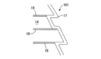
以上説明した本発明に係る圧電/電歪構造体の実施形態は、本発明に係る第1の圧電/電歪構造体、及び、本発明に係る第2の圧電/電歪構造体に共通する実施形態であるが、以下に、本発明に係る第2の圧電/電歪構造体のみに関わるシート状の圧電/電歪体と絶縁膜の熱膨張率について説明する。本発明に係る第2の圧電/電歪構造体は、薄膜に少なくとも絶縁膜が含まれるものであるから、図5(a)〜図9により説明した圧電/電歪構造体の全てが本発明に係る第2の圧電/電歪構造体として適用可能である。 The embodiment of the piezoelectric / electrostrictive structure according to the present invention described above is common to the first piezoelectric / electrostrictive structure according to the present invention and the second piezoelectric / electrostrictive structure according to the present invention. Although it is embodiment, the thermal expansion coefficient of the sheet-like piezoelectric / electrostrictive body and the insulating film related only to the second piezoelectric / electrostrictive structure according to the present invention will be described below. Since the second piezoelectric / electrostrictive structure according to the present invention includes at least an insulating film in the thin film, all of the piezoelectric / electrostrictive structures described with reference to FIGS. The second piezoelectric / electrostrictive structure according to the present invention can be applied.
先ず、複数のシート状の圧電/電歪体の積層界面が露出する側面に、薄膜として絶縁膜のみが形成される圧電/電歪構造体の場合(薄膜が一の単層膜で構成される場合)を例示して説明する。既に説明した図7(a)、図7(b)に示される圧電/電歪構造体71は、薄膜は絶縁膜ではなく保護膜であるが、一の単層膜で構成されており、この態様に該当する。
First, in the case of a piezoelectric / electrostrictive structure in which only an insulating film is formed as a thin film on the side surface where the laminated interface of a plurality of sheet-like piezoelectric / electrostrictive bodies is exposed (the thin film is composed of one single layer film) Case) will be described as an example. The piezoelectric /
例えば、圧電/電歪体を構成する材料として、チタン酸バリウム(BaTiO3、線膨
張係数α=13×10-6(/K))を採用したときに、絶縁膜として酸化タンタル(Ta2O5、α=3.6×10-6(/K))を用いることが好ましい。この熱膨張率差により絶縁膜の残留応力は圧縮応力となる。
For example, when barium titanate (BaTiO 3 , linear expansion coefficient α = 13 × 10 −6 (/ K)) is adopted as a material constituting the piezoelectric / electrostrictive body, tantalum oxide (Ta 2 O) is used as the insulating film. 5 and α = 3.6 × 10 −6 (/ K)) are preferably used. Due to this difference in thermal expansion coefficient, the residual stress of the insulating film becomes a compressive stress.
絶縁膜の材料として、Ta2O5以外に、酸化珪素(SiO2、α=0.5×10⁻⁶(/
K))、酸化アルミニウム(Al2O3、α=8.0×10⁻⁶(/K))、酸化ハフニウム(HfO2、α=6.3×10-6(/K)))、酸化ニオブ(Nb2O5、α=1.6×10-6(/K))、酸化イットリウム(Y2O3、α=7.9×10-6(/K))、酸化ジルコニウム(ZrO2、α=6.9×10-6(/K))等を採用出来る。酸化物ではないものとしては、窒化珪素(Si3N4、α=2.7×10-6(/K))、窒化アルミニウム(AlN、α=4.9×10-6(/K))、窒化ホウ素(BN、α=3.9×10-6(/K))等が挙げられる。又、以上のような単一の酸化物、窒化物ではなく、2種以上の混晶を用いることも可能である。
In addition to Ta 2 O 5 , silicon oxide (SiO 2 , α = 0.5 × 10 −6 (/
K)), aluminum oxide (Al 2 O 3 , α = 8.0 × 10 −6 (/ K)), hafnium oxide (HfO 2 , α = 6.3 × 10 −6 (/ K))), oxidation Niobium (Nb 2 O 5 , α = 1.6 × 10 −6 (/ K)), yttrium oxide (Y 2 O 3 , α = 7.9 × 10 −6 (/ K)), zirconium oxide (ZrO 2) , Α = 6.9 × 10 −6 (/ K)) or the like. Non-oxides include silicon nitride (Si 3 N 4 , α = 2.7 × 10 −6 (/ K)), aluminum nitride (AlN, α = 4.9 × 10 −6 (/ K)). And boron nitride (BN, α = 3.9 × 10 −6 (/ K)). It is also possible to use two or more mixed crystals instead of the single oxide or nitride as described above.
混晶を用いる理由としては、熱膨張率の極大きい材料(例えば、酸化マグネシウム(MgO、α=13.4×10⁻⁶(/K))と、極小さい材料(例えば、二酸化珪素(SiO2、α=0.5×10-6(/K))の組成比を自由に制御出来るからである。即ち、混晶の熱膨張率の設計が可能になり、圧電/電歪体を構成する材料に対し好適な熱膨張率を選択することにより、圧電/電歪構造体の強度設計が可能になる。 The reason why the mixed crystal is used is that a material having a very high thermal expansion coefficient (for example, magnesium oxide (MgO, α = 13.4 × 10 −6 (/ K)) and a very small material (for example, silicon dioxide (SiO 2) , Α = 0.5 × 10 −6 (/ K)) can be freely controlled, that is, the thermal expansion coefficient of the mixed crystal can be designed, and the piezoelectric / electrostrictive body is formed. By selecting a suitable coefficient of thermal expansion for the material, it is possible to design the strength of the piezoelectric / electrostrictive structure.
次に、複数のシート状の圧電/電歪体の積層界面が露出する側面に、薄膜として電極膜が形成され更にそれを覆うように絶縁膜が形成される圧電/電歪構造体の場合(薄膜が二の多層膜で構成される場合)について説明する。既に説明した圧電/電歪構造体51,61,81,91が該当する。このような薄膜が二の多層膜で構成される場合には、その熱膨張率を、絶縁膜、電極膜、圧電/電歪体(材料)の順に、小、大、中(又は中、大、小)にすること、即ち、電極膜の熱膨張率を最も大きくすることが肝要である。このような熱膨張率の組み合せで圧電/電歪構造体を設計すると、絶縁膜とシート状の圧電/電歪体の残留応力が、ともに圧縮応力になり、絶縁膜への残留応力を圧縮力とするのみならず、圧電/電歪構造体への残留応力も圧縮力となることで圧電/電歪構造体の強度がより向上する。
Next, in the case of a piezoelectric / electrostrictive structure in which an electrode film is formed as a thin film on a side surface where a laminated interface of a plurality of sheet-like piezoelectric / electrostrictive bodies is exposed, and an insulating film is formed so as to cover the electrode film ( The case where the thin film is composed of two multilayer films will be described. The piezoelectric /
例えば、絶縁膜として酸化タンタル(Ta2O5、α=3.6×10-6(/K))、電極膜として銅(Cu、α=17×10-6(/K))、シート状の圧電/電歪体としてチタン酸バリウム(BaTiO3、α=13×10-6(/K))を採用出来る。電極膜のバリア膜を形成する場合、その厚さが極薄いことから、応力に及ぼす影響は無視出来る。薄膜が絶縁膜のみの場合には、シート状の圧電/電歪体として熱膨張率が比較的小さいジルコン酸チタン酸鉛を採用すると、絶縁膜の熱膨張率を更に小さくとらねばならず、適用可能な材料が限られてしまうが、薄膜が二の多層膜で構成される場合には、絶縁膜と圧電/電歪体(材料)の熱膨張率関係が逆転しても、電極膜の熱膨張率が最大であれば強度向上の効果が得られるため、適用範囲が広がる。例えば、絶縁膜を酸化アルミニウム(Al2O3、α=8.0×10-6(/K))、電極膜を銅(Cu、α=17×10-6(/K))、シート状の圧電/電歪体をジルコン酸チタン酸鉛(PZT、α=3×10-6(/K))としてもよい。又、電極膜の材料は、金属以外の酸化物導電体を適用することも出来る。例えば、酸化イリジウム(IrO2、α=5.8×10-6(/K))、酸化ルテニウム(RuO2、α=6.4×10-6(/K))が例示される。これらの酸化物電極には、拡散防止膜としての機能も有するため、バリア膜を省略しても耐久性良好な圧電/電歪構造体が得られる。 For example, tantalum oxide (Ta 2 O 5 , α = 3.6 × 10 −6 (/ K)) as the insulating film, copper (Cu, α = 17 × 10 −6 (/ K)) as the electrode film, sheet shape As the piezoelectric / electrostrictive body, barium titanate (BaTiO 3 , α = 13 × 10 −6 (/ K)) can be adopted. When the barrier film of the electrode film is formed, since the thickness is extremely thin, the influence on the stress can be ignored. If the thin film is only an insulating film, the use of lead zirconate titanate, which has a relatively low thermal expansion coefficient as the sheet-like piezoelectric / electrostrictive body, requires that the thermal expansion coefficient of the insulating film be further reduced and applied. Although the possible materials are limited, when the thin film is composed of two multilayer films, the heat of the electrode film is maintained even if the thermal expansion coefficient relationship between the insulating film and the piezoelectric / electrostrictive body (material) is reversed. Since the effect of improving the strength can be obtained if the expansion coefficient is the maximum, the applicable range is expanded. For example, the insulating film is aluminum oxide (Al 2 O 3 , α = 8.0 × 10 −6 (/ K)), the electrode film is copper (Cu, α = 17 × 10 −6 (/ K)), a sheet shape The piezoelectric / electrostrictive body may be lead zirconate titanate (PZT, α = 3 × 10 −6 (/ K)). In addition, an oxide conductor other than metal can be applied as the material of the electrode film. Examples thereof include iridium oxide (IrO 2 , α = 5.8 × 10 −6 (/ K)) and ruthenium oxide (RuO 2 , α = 6.4 × 10 −6 (/ K)). Since these oxide electrodes also have a function as a diffusion preventing film, a piezoelectric / electrostrictive structure with good durability can be obtained even if the barrier film is omitted.
次に、本発明に係る圧電/電歪構造体の製造方法について説明する。本発明に係る圧電/電歪構造体の製造方法の概略工程の一例を、図10(a)〜図10(c)に示す。作製対象は、図16(a)、図16(b)に示される圧電/電歪構造体161と同態様の圧電/電歪構造体である。
Next, a method for manufacturing a piezoelectric / electrostrictive structure according to the present invention will be described. An example of a schematic process of the method for manufacturing a piezoelectric / electrostrictive structure according to the present invention is shown in FIGS. 10 (a) to 10 (c). The object to be manufactured is a piezoelectric / electrostrictive structure having the same form as the piezoelectric /
以下、製造工程について説明する。先ず、圧電/電歪材料を主成分とする所定枚数のセラミックグリーンシートを用意する。セラミックグリーンシートは、従来知られた方法により作製出来る。例えば、圧電/電歪材料粉末を用意し、これにバインダ、溶剤、分散剤、可塑剤等を望む組成に調合してスラリーを作製し、これを脱泡処理後、ドクターブレード法、リバースロールコーター法等のグリーンシート成形法によって、セラミックグリーンシートを形成することが可能である。 Hereinafter, the manufacturing process will be described. First, a predetermined number of ceramic green sheets mainly comprising a piezoelectric / electrostrictive material are prepared. The ceramic green sheet can be produced by a conventionally known method. For example, a piezoelectric / electrostrictive material powder is prepared, and a binder, a solvent, a dispersant, a plasticizer, and the like are mixed into a desired composition to prepare a slurry. After defoaming, a doctor blade method, a reverse roll coater A ceramic green sheet can be formed by a green sheet forming method such as a method.
得られたセラミックグリーンシートに対し、例えばパンチとダイによる打抜加工により、図10(a)に示されるような、グリーンシート602,615,619を得る。グリーンシート602,619は各1枚でよく、グリーンシート615は複数枚用意する。グリーンシート615は、のちにセルを構成するスリット孔605、のちにダミーセルを構成するスリット孔625、のちに個別配線用のビアホールを構成する円孔628、及びのちに共通配線用のビアホールを構成する円孔629が形成されたグリーンシートである。グリーンシート602は、のちに底板を構成するものであり、のちにダミーセルを構成するスリット孔625が形成されたグリーンシートである。グリーンシート619は、のちに(インクジェットヘッドとしての)ノズル板を構成するものであり、のちにダミーセルを構成するスリット孔625と、のちにノズルを構成する円孔608が形成されたグリーンシートである。尚、各1枚作製するグリーンシート602とグリーンシート619については、圧電/電歪材料を主成分とはしない別の材料を用いてもよい。
For the obtained ceramic green sheet,
次に、図10(b)に示されるように、複数枚のグリーンシート615の円孔628,629を導電材料で埋めてビアホール128,129を形成するとともに、そのグリーンシート615の半々ずつに、ビアホール128に接続される導体膜(導電材料からなる膜)318、及びビアホール129に接続される導体膜319を形成して、それぞれ複数枚のグリーンシート614,616を得る。導体膜のパターニングは予めフォトレジストを塗布し露光することで行ってもよいし、全面成膜後に不必要な部分を研削等の手法により切除してもよい。
Next, as shown in FIG. 10B, the
グリーンシート614,616において、6つのスリット孔605はのちにセルを構成する孔であり、スリット孔625に対し相対的に大きく開けられる。7つのスリット孔625は、のちにセルとセルとの間の空間であるダミーセルを構成する孔であり、スリット孔605を挟むように配置される。スリット孔605とスリット孔625との間のグリーンシート実体部分が、のちに側壁を構成する。導体膜318は、個別配線に用いられ、その端部が、のちにセルを構成するスリット孔605を形成する面に露出されるように設けられる。導体膜319は、共通配線に用いられ、のちにダミーセルを構成するスリット孔625を形成する面に露出されるように設けられる。尚、導体膜はスクリーン印刷等の手法により所定のパターンで形成出来る。
In the
次に、グリーンシート602の上に、セルを形成するために複数のグリーンシート614,616を交互に積層し、圧着して所定の厚さを有するセラミックグリーン積層体を得て、それを焼成一体化して焼成積層体を得る(図示しない)。この焼成積層体は、グリーンシート614,616のスリット孔605を連通させてなる6つのセルと、グリーンシート602,614,616のスリット孔625を連通させてなる7つのダミーセルと、を備えている。尚、グリーンシート619は、別途焼成し、ノズル板9として用いられる(図10(c)参照)。
Next, a plurality of
次いで、焼成積層体に対して、CVD成膜法によって、セルを形成する面とダミーセルを形成する面に、保護膜を形成する。そして、必要に応じて、外部配線接続、圧電/電歪体の分極処理を施せば、圧電/電歪構造体611が得られ、更にノズル板9を接着すれば、インクジェットヘッド601を得ることが出来る(図10(c))。インクジェットヘッド601において、ダミーセル15とノズル8は外観に現れるが、セルは圧電/電歪構造体611の内部に形成され露わになっていない。
Next, a protective film is formed on the surface on which the cells are to be formed and the surface on which the dummy cells are to be formed on the fired laminate by a CVD film forming method. If necessary, the piezoelectric /
本発明に係る圧電/電歪構造体の製造方法では、CVD(化学気相成長)成膜法を用いて、上記工程にかかる電極膜(導体膜)及び保護膜の形成の他、絶縁膜、防湿膜の形成も行う。CVD成膜法によれば、分子レベルのガス成分がシート状の圧電/電歪体上に到達することで成膜されるため、シート状の圧電/電歪体の(セラミックス)粒子の間にガスが入り込み、カバーレッジのよい緻密な膜が形成される。 In the method for manufacturing a piezoelectric / electrostrictive structure according to the present invention, the CVD (chemical vapor deposition) film forming method is used to form an electrode film (conductor film) and a protective film according to the above process, an insulating film, A moisture barrier film is also formed. According to the CVD film formation method, a film component is formed when a gas component at a molecular level reaches the sheet-like piezoelectric / electrostrictive body, and therefore between the (ceramic) particles of the sheet-like piezoelectric / electrostrictive body. Gas enters and a dense film with good coverage is formed.
成膜法としては、CVD成膜法の他に、電気泳動法、陽極酸化法、ペースト塗布法、スパッタ法、蒸着重合法等が知られている。電気泳動法は、電気化学的な駆動力により選択的に成膜出来るが溶液プロセスで堆積した膜を焼成することで膜形成を行う方法であるから、気孔を多く含む膜しか形成出来ない。又、陽極酸化法は、電極成分を選択的に酸化することで皮膜を形成する手法であり、溶液中で膜形成を行い膜の焼成は必要としないが、電気泳動法と同様に緻密な膜を得ることは出来ない。本発明に係る圧電/電歪構造体の製造方法では、成膜対象はグリーンシート積層法で得られた積層構造を有する圧電/電歪構造体であり、1枚のグリーンシートの端面(開口端面)がテーパー状になることに基づいて、圧電/電歪構造体には、複数のシート状の圧電/電歪体の積層界面に切欠が形成され、その切欠の開口幅や深さのサイズはミクロンオーダーである。従って、この切欠にかかる未接合部を補強し構造体の強度アップを図る目的には、両方法は適切な手段とはいえない。 As the film forming method, in addition to the CVD film forming method, an electrophoresis method, an anodic oxidation method, a paste coating method, a sputtering method, a vapor deposition polymerization method, and the like are known. The electrophoresis method can selectively form a film by an electrochemical driving force, but is a method of forming a film by baking a film deposited by a solution process. Therefore, only a film having many pores can be formed. The anodic oxidation method is a method of forming a film by selectively oxidizing electrode components. The film is formed in a solution and does not need to be baked. Can not get. In the method for manufacturing a piezoelectric / electrostrictive structure according to the present invention, a film formation target is a piezoelectric / electrostrictive structure having a laminated structure obtained by a green sheet laminating method, and an end face (opening end face) of one green sheet. ) Is tapered, the piezoelectric / electrostrictive structure has a plurality of sheet-like piezoelectric / electrostrictive layer stacks formed with notches, and the size of the opening width and depth of the notches is Micron order. Therefore, both methods are not appropriate means for the purpose of reinforcing the unjoined portion of the notch and increasing the strength of the structure.
ペースト塗布法は、焼成前の(セラミックグリーン)積層体における複数のグリーンシートによる積層界面にペーストを塗布して焼成する方法である(本出願人による特願2002−334097を参照)。具体的には、ペースト材料を作製し、スピンコート等の手段で塗布し、切欠の未接合部を埋設し一体焼成することで、切欠をなくし、滑らかな表面を得ることが出来る。ペーストを使用することから、その表面張力により、極狭い空間に対しては実現が困難であり、高アスペクト比が求められる本発明に係る圧電/電歪構造体の製造方法としては適切ではない。又、なによりも滑らかな表面になってしまうから、本発明に係る圧電/電歪構造体の特徴である、複数のシート状の圧電/電歪体の積層界面が露出する側面に形成された切欠が現す凹凸面に沿って、即ち凹凸を残したまま、薄膜を形成するのには適していない。 The paste application method is a method in which a paste is applied to a laminated interface of a plurality of green sheets in a (ceramic green) laminate before firing and fired (see Japanese Patent Application No. 2002-334097 by the present applicant). Specifically, a paste material is prepared, applied by means such as spin coating, and the unjoined portion of the notch is embedded and integrally fired, thereby eliminating the notch and obtaining a smooth surface. Since the paste is used, it is difficult to realize it in an extremely narrow space due to its surface tension, and it is not suitable as a method for manufacturing a piezoelectric / electrostrictive structure according to the present invention which requires a high aspect ratio. In addition, since the surface becomes smoother than the other, it is formed on the side surface where the laminated interface of the plurality of sheet-like piezoelectric / electrostrictive bodies, which is a feature of the piezoelectric / electrostrictive structure according to the present invention, is exposed. It is not suitable for forming a thin film along the uneven surface where the notch appears, that is, while leaving the unevenness.
スパッタ法や蒸着法等のPVD(物理気相成長法)による方法は、指向性が強いため、高アスペクト比な圧電/電歪構造体へ成膜する手段としては適切なものではない。図4は、切欠を誇張して描いた圧電/電歪構造体の断面図であり、一例としてスパッタ法による成膜の様子を表した図である。例えばノズル板でセル3を塞ぐ前に、セル3を形成する側壁6の表面に成膜材料40を成膜しようとしても、切欠における、成膜方向(図4中の矢印方向)から影になる部分には、原理的に成膜されず、有用な方法ではない。成膜角度の最適化やコリメートスパッタ等の手法を用いても、アスペクト比5程度の圧電/電歪構造体に対して成膜することが限界であった。
PVD (physical vapor deposition) methods such as sputtering and vapor deposition have strong directivity and are not suitable as means for forming a film on a high aspect ratio piezoelectric / electrostrictive structure. FIG. 4 is a cross-sectional view of a piezoelectric / electrostrictive structure drawn with exaggerated notches, and shows a state of film formation by sputtering as an example. For example, before the
一方、蒸着重合法は、CVD法の代わりに好ましい手段として採用出来る。蒸着重合法とは、基板上に、両末端に官能性を有する複数のモノマーを気相で蒸着、反応させ、高分子の薄膜を形成する方法であり、例えば分子鎖が高度に配向、配列した有機薄膜を作製出来る。ポリイミド、ポリ尿素等が成膜可能な方法である。 On the other hand, the vapor deposition polymerization method can be employed as a preferable means instead of the CVD method. The vapor deposition polymerization method is a method in which a plurality of monomers having functionalities at both ends are vapor-deposited and reacted on a substrate to form a polymer thin film. For example, molecular chains are highly oriented and arranged. Organic thin film can be produced. In this method, polyimide, polyurea or the like can be formed.
以下、CVD成膜法について、使用する材料(原料)を例示しながら説明する。図12は、CVD成膜法に使用されるMOCVD(有機金属化学気相成長法)成膜装置の概略の構成図である。キャリアガスとしてアルゴン(Ar)、窒素(N2)を使用し、反応ガスとして酸素(O2)、アンモニア(NH3)が使用される。成膜に用いる原料は、各々ステンレス製容器に封入され、温度制御された別々のオーブンに備えられる。リアクタ(Reactor)は、石英製の2重管構造となっており、インナー管(inner tube)は横型の構成である。基板加熱はヒーター(Heater)により行い、排気(exhaust)はロータリーポンプ(RP)とターボ分子ポンプ(TP)により行われる。 Hereinafter, the CVD film forming method will be described with reference to materials (raw materials) to be used. FIG. 12 is a schematic configuration diagram of an MOCVD (metal organic chemical vapor deposition) film forming apparatus used for the CVD film forming method. Argon (Ar) and nitrogen (N 2 ) are used as the carrier gas, and oxygen (O 2 ) and ammonia (NH 3 ) are used as the reaction gas. The raw materials used for film formation are each enclosed in a stainless steel container and provided in a separate oven with temperature control. The reactor has a double tube structure made of quartz, and the inner tube has a horizontal configuration. Substrate heating is performed by a heater, and exhaust is performed by a rotary pump (RP) and a turbo molecular pump (TP).
例えば、絶縁膜として酸化タンタル(Ta2O5)を、バリア膜としては窒化チタン(TiN)を、電極層としては銅(Cu)を形成する条件について、以下に記載する。オーブンAにTa系原料を(Oven A(Ta))、オーブンBにTi系原料を(Oven B(Ti))、オーブンCにCu系原料を(Oven C(Cu))、それぞれ備え、各々のオーブンからリアクタへ、独立した配管で接続されており、リアクタへ、それぞれINLET 1、INLET 2、INLET 3により導入される。
For example, conditions for forming tantalum oxide (Ta 2 O 5 ) as an insulating film, titanium nitride (TiN) as a barrier film, and copper (Cu) as an electrode layer are described below. The oven A is provided with a Ta-based material (Oven A (Ta)), the oven B with a Ti-based material (Oven B (Ti)), and the oven C with a Cu-based material (Oven C (Cu)). It is connected to the reactor from the oven by an independent pipe, and is introduced into the reactor by
(絶縁膜の形成)ペンタエトキシタンタル(Ta(OC2H5)5)を原料として使用し
、絶縁膜としてTa2O5膜を成膜した。MOCVD成膜装置において、115℃に加熱されたオーブンA(Oven A(Ta))内に装着された原料は、Arキャリアガスより搬送され、INLET 1からリアクタへ導入される。反応ガスとしては酸素を使用する。成膜温度は600℃、成膜圧力は1300Pa、形成した絶縁膜の厚さは2μm、成膜時間は2時間である。
(Formation of Insulating Film) Pentaethoxytantalum (Ta (OC 2 H 5 ) 5 ) was used as a raw material, and a Ta 2 O 5 film was formed as an insulating film. In the MOCVD film forming apparatus, the raw material mounted in the oven A (Oven A (Ta)) heated to 115 ° C. is transported from the Ar carrier gas and introduced into the reactor from the
(バリア膜の形成)テトラキスジエチルアミドチタニウム(TDEAT Ti[N(C2H5)2]4)を原料として使用し、バリア膜としてTiN膜を成膜した。MOCVD成膜装置において、オーブンB(Oven B(Ti))に装着された原料は、マスフローコントローラー(MFC)と100℃に加熱した気化器(V)を用いてリアクタへ供給される。キャリアガスとしてN2を、反応ガスとしてNH3を使用する。成膜温度は350℃、成膜圧力は10Pa、形成した絶縁膜の厚さは50nm、成膜時間は5分である。尚、TiN以外のバリア膜として、窒化タンタル(TaN)、窒化ニオブ(NbN)等を採用することが出来る。 (Formation of Barrier Film) Tetrakis diethylamido titanium (TDEAT Ti [N (C 2 H 5 ) 2 ] 4 ) was used as a raw material, and a TiN film was formed as a barrier film. In the MOCVD film forming apparatus, the raw material mounted in the oven B (Oven B (Ti)) is supplied to the reactor using a mass flow controller (MFC) and a vaporizer (V) heated to 100 ° C. N 2 is used as a carrier gas and NH 3 is used as a reaction gas. The film formation temperature is 350 ° C., the film formation pressure is 10 Pa, the thickness of the formed insulating film is 50 nm, and the film formation time is 5 minutes. As the barrier film other than TiN, tantalum nitride (TaN), niobium nitride (NbN), or the like can be used.
(電極膜の形成)銅ヘキサフルオロアセチルアセテートトリメチルビニルシラン(Cu(hfac)(tmvs))を原料として使用し、電極膜としてCu膜を成膜した。MOCVD成膜装置において、オーブンC(Oven C(Cu))に装着された原料は、マスフローコントローラー(MFC)と気化器(V)を用いてリアクタへ供給される。キャリアガスとしてはArが用いられる。成膜温度は210℃、成膜圧力は200Pa、形成した絶縁膜の厚さは2μm、成膜時間は20分である。 (Formation of electrode film) Copper hexafluoroacetyl acetate trimethylvinylsilane (Cu (hfac) (tmvs)) was used as a raw material, and a Cu film was formed as an electrode film. In the MOCVD film forming apparatus, the raw material attached to the oven C (Oven C (Cu)) is supplied to the reactor using a mass flow controller (MFC) and a vaporizer (V). Ar is used as the carrier gas. The film forming temperature is 210 ° C., the film forming pressure is 200 Pa, the thickness of the formed insulating film is 2 μm, and the film forming time is 20 minutes.
尚、上記の例に示した材料(原料)の他に、CVD法により成膜可能な材料として、パリレン樹脂がある。パリレン樹脂は、常温で成膜可能な有機材料であり、絶縁性、耐薬品性、撥水性を有する材料であることから、本発明にかかる絶縁膜、保護膜、防湿膜としての機能を併せ持つ優れた材料である。 In addition to the material (raw material) shown in the above example, there is a parylene resin as a material that can be formed by a CVD method. Parylene resin is an organic material that can be formed at room temperature, and is an insulating, chemical-resistant, and water-repellent material, so it has excellent functions as an insulating film, protective film, and moisture-proof film according to the present invention. Material.
本発明に係る圧電/電歪構造体は、印刷機器のインクジェットヘッドに適用される他に、本出願人による国際出願にかかる国際公開公報、WO 02/084751 A1に記されているように、DNAチップ製造装置、光スイッチ、マイクロミラー、マイクロマシン搬送装置のアクチュエータ部としての利用が可能である。更に、マイクロポンプ、半導体製造用のコーティング装置、複雑で微細な3次元構造体の作製装置、製薬分野における薬品合成装置等のアクチュエータ部としても好ましく採用され得る。 The piezoelectric / electrostrictive structure according to the present invention is applied to an ink jet head of a printing device, as well as a DNA as described in International Publication No. WO 02/084751 A1 relating to an international application by the present applicant. It can be used as an actuator part of a chip manufacturing device, an optical switch, a micromirror, or a micromachine transfer device. Furthermore, it can be preferably employed as an actuator unit for a micropump, a coating device for manufacturing a semiconductor, a device for producing a complicated and fine three-dimensional structure, a chemical synthesis device in the pharmaceutical field, and the like.
1,130,601…インクジェットヘッド、2…底板、3…セル、4…圧電/電歪作動部、5…インク室、6…側壁、8…ノズル、9…ノズル板、11…アクチュエータ(圧電/電歪構造体)、14…圧電/電歪体、15…ダミーセル、16,602,615,619…グリーンシート、17…保護膜、18,19…電極層、28,29…電極膜、25…切欠、32…未接合部、51,61,71,81,91,161,611…圧電/電歪構造体、100…切断線、110…薄膜、131…アクチュエータ、132…基板、133…セル、134…圧電/電歪作動部、135…インク室、136…側壁、137…蓋板、138…ノズル、139…ノズル板、143…セラミックグリーン積層体、177…絶縁膜、318,319…導体膜、605,625…スリット孔、628,629…円孔。
DESCRIPTION OF SYMBOLS 1,130,601 ... Inkjet head, 2 ... Bottom plate, 3 ... Cell, 4 ... Piezoelectric / electrostrictive operation part, 5 ... Ink chamber, 6 ... Side wall, 8 ... Nozzle, 9 ... Nozzle plate, 11 ... Actuator (piezoelectric / Electrostrictive structure), 14 ... Piezoelectric / electrostrictive body, 15 ... Dummy cell, 16,602,615,619 ... Green sheet, 17 ... Protective film, 18,19 ... Electrode layer, 28,29 ... Electrode film, 25 ... Notch, 32 ... unjoined part, 51, 61, 71, 81, 91, 161, 611 ... piezoelectric / electrostrictive structure, 100 ... cutting line, 110 ... thin film, 131 ... actuator, 132 ... substrate, 133 ... cell, 134: Piezoelectric / electrostrictive actuator, 135: Ink chamber, 136: Side wall, 137 ... Lid plate, 138 ... Nozzle, 139 ... Nozzle plate, 143 ... Ceramic green laminate, 177 ... Insulating film, 318, 319 ...
Claims (20)
前記複数のシート状の圧電/電歪体の積層界面が露出する側面に複数の切欠が形成され、前記切欠が現す凹凸面に沿って、その凹凸状態が表されたままに、1層以上の薄膜が形成されている圧電/電歪構造体。 A piezoelectric / electrostrictive structure formed by laminating a plurality of sheet-like piezoelectric / electrostrictive bodies,
A plurality of notches are formed on the side surface where the laminated interface of the plurality of sheet-like piezoelectric / electrostrictive bodies is exposed , and the uneven state is expressed along the uneven surface where the notches appear. A piezoelectric / electrostrictive structure in which a thin film is formed.
前記複数のシート状の圧電/電歪体の積層界面が露出する側面に複数の切欠が形成され、前記切欠が現す凹凸面に沿って、その凹凸状態が表されたままに、1層以上の薄膜が形成され、
前記1層以上の薄膜が、絶縁膜、保護膜、防湿膜からなる膜群から選ばれる一の単層膜又は二以上の多層膜で構成されるとともに、
前記薄膜の熱膨張率が前記圧電/電歪体の熱膨張率より小さい圧電/電歪構造体。 A piezoelectric / electrostrictive structure formed by laminating a plurality of sheet-like piezoelectric / electrostrictive bodies,
A plurality of notches are formed on the side surface where the laminated interface of the plurality of sheet-like piezoelectric / electrostrictive bodies is exposed , and the uneven state is expressed along the uneven surface where the notches appear. A thin film is formed,
The one or more thin films are composed of one single-layer film or two or more multilayer films selected from a film group consisting of an insulating film, a protective film, and a moisture-proof film.
A piezoelectric / electrostrictive structure having a coefficient of thermal expansion smaller than that of the piezoelectric / electrostrictive body.
得られた前記圧電/電歪焼成体の、前記積層界面が露出する側面に形成された、前記切欠が現す凹凸面に沿って、その凹凸状態が表されたままに、CVD成膜法によって、1層以上の薄膜を形成して圧電/電歪構造体を得る工程と、
を有する圧電/電歪構造体の製造方法。 Laminating and firing a plurality of ceramic green sheets made of a piezoelectric / electrostrictive material, and obtaining a piezoelectric / electrostrictive fired body having a plurality of notches formed on the side surface where the lamination interface based on the plurality of ceramic green sheets is exposed When,
The obtained piezoelectric / electrostrictive fired body is formed on the side surface where the lamination interface is exposed , along the uneven surface where the notch appears, while the uneven state is expressed by the CVD film forming method, Forming a piezoelectric / electrostrictive structure by forming one or more thin films;
A method for manufacturing a piezoelectric / electrostrictive structure having:
前記CVD成膜法にかかるCVD材料として、アルコキシド系有機金属化合物、乃至、β−ジケトン系有機金属化合物を使用する請求項16〜19の何れか一項に記載の圧電/電歪構造体の製造方法。 The one or more thin films are composed of one single-layer film or two or more multilayer films selected from a film group consisting of an insulating film, a protective film, and a moisture-proof film.
20. The piezoelectric / electrostrictive structure according to claim 16, wherein an alkoxide-based organometallic compound or a β-diketone-based organometallic compound is used as a CVD material according to the CVD film forming method. Method.
Priority Applications (4)
| Application Number | Priority Date | Filing Date | Title |
|---|---|---|---|
| JP2005115428A JP4847039B2 (en) | 2004-05-28 | 2005-04-13 | Piezoelectric / electrostrictive structure and method for manufacturing piezoelectric / electrostrictive structure |
| US11/138,250 US7274134B2 (en) | 2004-05-28 | 2005-05-26 | Piezoelectric/electrostrictive structure and method for manufacturing the same |
| DE200560024210 DE602005024210D1 (en) | 2004-05-28 | 2005-05-27 | Piezoelectric / electrostrictive structure and manufacturing method therefor |
| EP20050253301 EP1608031B1 (en) | 2004-05-28 | 2005-05-27 | Piezoelectric/electrostrictive structure and method for manufacturing the same |
Applications Claiming Priority (3)
| Application Number | Priority Date | Filing Date | Title |
|---|---|---|---|
| JP2004159779 | 2004-05-28 | ||
| JP2004159779 | 2004-05-28 | ||
| JP2005115428A JP4847039B2 (en) | 2004-05-28 | 2005-04-13 | Piezoelectric / electrostrictive structure and method for manufacturing piezoelectric / electrostrictive structure |
Publications (2)
| Publication Number | Publication Date |
|---|---|
| JP2006013442A JP2006013442A (en) | 2006-01-12 |
| JP4847039B2 true JP4847039B2 (en) | 2011-12-28 |
Family
ID=35134235
Family Applications (1)
| Application Number | Title | Priority Date | Filing Date |
|---|---|---|---|
| JP2005115428A Expired - Fee Related JP4847039B2 (en) | 2004-05-28 | 2005-04-13 | Piezoelectric / electrostrictive structure and method for manufacturing piezoelectric / electrostrictive structure |
Country Status (4)
| Country | Link |
|---|---|
| US (1) | US7274134B2 (en) |
| EP (1) | EP1608031B1 (en) |
| JP (1) | JP4847039B2 (en) |
| DE (1) | DE602005024210D1 (en) |
Families Citing this family (16)
| Publication number | Priority date | Publication date | Assignee | Title |
|---|---|---|---|---|
| JP4736422B2 (en) * | 2004-12-24 | 2011-07-27 | 株式会社デンソー | Manufacturing method of multilayer piezoelectric element |
| JP5123491B2 (en) * | 2005-06-10 | 2013-01-23 | 日本碍子株式会社 | Multilayer piezoelectric / electrostrictive element |
| JP2007243066A (en) * | 2006-03-10 | 2007-09-20 | Denso Corp | Stacked piezoelectric element and its manufacturing method |
| US8833174B2 (en) * | 2007-04-12 | 2014-09-16 | Colorado School Of Mines | Piezoelectric sensor based smart-die structure for predicting the onset of failure during die casting operations |
| JP5225392B2 (en) * | 2008-02-05 | 2013-07-03 | モルガン アドバンスド セラミックス, インコーポレイテッド | Encapsulation coating to reduce particle shedding |
| JP5743069B2 (en) * | 2011-03-15 | 2015-07-01 | セイコーエプソン株式会社 | Piezoelectric element, liquid ejecting head, and liquid ejecting apparatus |
| JP5836755B2 (en) * | 2011-10-04 | 2015-12-24 | 富士フイルム株式会社 | Piezoelectric element and liquid discharge head |
| JP5919775B2 (en) * | 2011-12-01 | 2016-05-18 | コニカミノルタ株式会社 | Droplet discharge head and recording apparatus |
| JP6064677B2 (en) * | 2013-02-28 | 2017-01-25 | セイコーエプソン株式会社 | Piezoelectric element, liquid ejecting head, liquid ejecting apparatus, and ultrasonic sensor |
| JP2015153850A (en) * | 2014-02-13 | 2015-08-24 | 株式会社サイオクス | Piezoelectric material thin film element, manufacturing method thereof, and electronic device with piezoelectric material thin film element |
| WO2016039138A1 (en) * | 2014-09-12 | 2016-03-17 | 株式会社村田製作所 | Stretchable film laminate and electronic device |
| JP2016060164A (en) * | 2014-09-19 | 2016-04-25 | セイコーエプソン株式会社 | Piezoelectric element, liquid injection head, liquid injection device and manufacturing method of piezoelectric element |
| FR3065348B1 (en) * | 2017-04-12 | 2022-06-24 | Safran Electronics & Defense | ELECTRONIC MODULE WITH IMPROVED PROTECTION AGAINST HUMIDITY |
| JP7087413B2 (en) * | 2018-01-31 | 2022-06-21 | セイコーエプソン株式会社 | Piezoelectric devices, liquid spray heads, and liquid sprayers |
| JP7451918B2 (en) | 2019-09-27 | 2024-03-19 | セイコーエプソン株式会社 | Liquid ejection head and liquid ejection device |
| KR20210124844A (en) * | 2020-04-07 | 2021-10-15 | 삼성전자주식회사 | Electronic device including ferroelectric material and method for manufacturing the electronic device |
Family Cites Families (27)
| Publication number | Priority date | Publication date | Assignee | Title |
|---|---|---|---|---|
| JPH02285685A (en) * | 1989-04-27 | 1990-11-22 | Fuji Electric Co Ltd | Laminated piezoelectric element |
| JPH0821734B2 (en) * | 1989-06-07 | 1996-03-04 | 株式会社村田製作所 | Electrostrictive actuator |
| JP2545639B2 (en) * | 1990-07-30 | 1996-10-23 | 富士通株式会社 | Multilayer piezoelectric element |
| JPH04214686A (en) * | 1990-10-05 | 1992-08-05 | Nec Corp | Electrostrictive effect element |
| JPH06334236A (en) * | 1993-05-20 | 1994-12-02 | Fujitsu Ltd | Manufacture of multilayer piezoelectric/electrostrictive actuator |
| JP3339599B2 (en) * | 1994-03-28 | 2002-10-28 | オリンパス光学工業株式会社 | Ferroelectric memory |
| WO1996014988A1 (en) * | 1994-11-14 | 1996-05-23 | Philips Electronics N.V. | Ink jet recording device and ink jet recording head |
| JP3217006B2 (en) | 1997-01-21 | 2001-10-09 | 日本電気株式会社 | Ink jet recording head and method of manufacturing the same |
| EP0857572B1 (en) * | 1997-01-14 | 2003-05-14 | Nec Corporation | Ink jet recording head having a piezoelectric substrate |
| JP3398574B2 (en) * | 1997-07-31 | 2003-04-21 | 富士通株式会社 | Manufacturing method of inkjet head |
| US6502302B2 (en) * | 2000-07-19 | 2003-01-07 | Ngk Insulators, Ltd. | Process for producing an industrial member having throughholes of high aspect ratio |
| JP4067782B2 (en) | 2000-07-19 | 2008-03-26 | 日本碍子株式会社 | Manufacturing method of industrial parts having through-holes with high aspect ratio |
| US6637102B2 (en) * | 2000-07-19 | 2003-10-28 | Ngk Insulators, Ltd. | Process for producing an industrial member having throughholes of high aspect ratio |
| US6700306B2 (en) * | 2001-02-27 | 2004-03-02 | Kyocera Corporation | Laminated piezo-electric device |
| JP3994877B2 (en) * | 2001-03-01 | 2007-10-24 | 日本碍子株式会社 | Comb-shaped piezoelectric actuator and manufacturing method thereof |
| DE10206115A1 (en) * | 2001-03-06 | 2002-09-19 | Ceramtec Ag | Piezoceramic multilayer actuators and a process for their production |
| JP3693939B2 (en) * | 2001-04-06 | 2005-09-14 | 日本碍子株式会社 | Cell-driven micropump member and manufacturing method |
| JP4931307B2 (en) * | 2001-09-27 | 2012-05-16 | 京セラ株式会社 | Bonding structure of piezoelectric ceramics and ink jet recording head using the same |
| JP4225033B2 (en) * | 2001-12-14 | 2009-02-18 | 株式会社日本自動車部品総合研究所 | Ceramic laminate and manufacturing method thereof |
| JP2003300328A (en) * | 2002-02-08 | 2003-10-21 | Konica Minolta Holdings Inc | Ink jet head and its fabricating method |
| JP2003243738A (en) * | 2002-02-15 | 2003-08-29 | Denso Corp | Stacked piezoelectric element |
| JP2003298131A (en) * | 2002-04-01 | 2003-10-17 | Mitsubishi Electric Corp | Piezoelectric thin film element and its manufacturing method |
| EP1382301B1 (en) * | 2002-07-19 | 2010-11-17 | Aloka Co. Ltd. | Ultrasonic probe and manufacturing method thereof |
| JP2004297041A (en) * | 2003-03-12 | 2004-10-21 | Denso Corp | Laminated piezoelectric element |
| JP4470504B2 (en) * | 2004-02-03 | 2010-06-02 | 株式会社デンソー | Multilayer piezoelectric element and method for manufacturing the same |
| DE102004047105A1 (en) * | 2004-09-29 | 2006-05-24 | Robert Bosch Gmbh | Piezo actuator with stress-relieving structures |
| JP5123491B2 (en) * | 2005-06-10 | 2013-01-23 | 日本碍子株式会社 | Multilayer piezoelectric / electrostrictive element |
-
2005
- 2005-04-13 JP JP2005115428A patent/JP4847039B2/en not_active Expired - Fee Related
- 2005-05-26 US US11/138,250 patent/US7274134B2/en not_active Expired - Fee Related
- 2005-05-27 EP EP20050253301 patent/EP1608031B1/en not_active Expired - Fee Related
- 2005-05-27 DE DE200560024210 patent/DE602005024210D1/en active Active
Also Published As
| Publication number | Publication date |
|---|---|
| EP1608031B1 (en) | 2010-10-20 |
| US7274134B2 (en) | 2007-09-25 |
| JP2006013442A (en) | 2006-01-12 |
| DE602005024210D1 (en) | 2010-12-02 |
| US20050264138A1 (en) | 2005-12-01 |
| EP1608031A3 (en) | 2008-04-02 |
| EP1608031A2 (en) | 2005-12-21 |
Similar Documents
| Publication | Publication Date | Title |
|---|---|---|
| JP4847039B2 (en) | Piezoelectric / electrostrictive structure and method for manufacturing piezoelectric / electrostrictive structure | |
| US6584660B1 (en) | Method of manufacturing a piezoelectric device | |
| US5643379A (en) | Method of producing a piezoelectric/electrostrictive actuator | |
| US7528530B2 (en) | Piezoelectric substance, piezoelectric substance element, liquid discharge head, liquid discharge device and method for producing piezoelectric substance | |
| JP2005313628A (en) | {100} oriented dielectric member, piezoelectric member, inkjet head, inkjet recording device, and method of producing the same | |
| JP5245107B2 (en) | Piezoelectric element, piezoelectric actuator, ink jet recording head | |
| JP2005277408A (en) | Dielectric element, piezoelectric element, ink-jet head and ink-jet recording device, and method of manufacturing same | |
| JP2005244133A (en) | Dielectric element, piezoelectric element, inkjet head, inkjet recording apparatus, and method of manufacturing the same | |
| JP2693291B2 (en) | Piezoelectric / electrostrictive actuator | |
| JP4250593B2 (en) | Dielectric element, piezoelectric element, ink jet head, and manufacturing method thereof | |
| US7677708B2 (en) | Discharge device | |
| US6993813B2 (en) | Method for manufacturing a piezoelectric/electrostrictive film-type actuator | |
| US8672458B2 (en) | Liquid ejecting head and liquid ejecting apparatus | |
| JP5121186B2 (en) | Piezoelectric body, piezoelectric element, liquid discharge head, and liquid discharge apparatus | |
| JP2006269916A (en) | Piezoelectric actuator and discharging device | |
| JP4878111B2 (en) | Cell driving type piezoelectric / electrostrictive actuator and manufacturing method thereof | |
| JP5260900B2 (en) | Liquid discharge head | |
| US7274133B2 (en) | Cell driving type piezoelectric actuator, and method of manufacturing cell driving type piezoelectric actuator | |
| JP2011091234A (en) | Liquid ejection head, liquid ejection device and actuator device | |
| KR100816169B1 (en) | Method for producing actuator device, actuator device, liquid-jet head and liquid-jet apparatus | |
| JP5144912B2 (en) | Multilayer piezoelectric actuator and print head | |
| JP2005014447A (en) | Print head and electronic apparatus | |
| JP2007267550A (en) | Piezoelectric actuator and polarization method therefor | |
| JP2009061729A (en) | Liquid injection head and liquid injection apparatus | |
| JP2009029019A (en) | Liquid jetting head and liquid jetting device |
Legal Events
| Date | Code | Title | Description |
|---|---|---|---|
| A621 | Written request for application examination |
Free format text: JAPANESE INTERMEDIATE CODE: A621 Effective date: 20070222 |
|
| A977 | Report on retrieval |
Free format text: JAPANESE INTERMEDIATE CODE: A971007 Effective date: 20101118 |
|
| A131 | Notification of reasons for refusal |
Free format text: JAPANESE INTERMEDIATE CODE: A131 Effective date: 20110215 |
|
| A521 | Request for written amendment filed |
Free format text: JAPANESE INTERMEDIATE CODE: A523 Effective date: 20110408 |
|
| TRDD | Decision of grant or rejection written | ||
| A01 | Written decision to grant a patent or to grant a registration (utility model) |
Free format text: JAPANESE INTERMEDIATE CODE: A01 Effective date: 20111011 |
|
| A01 | Written decision to grant a patent or to grant a registration (utility model) |
Free format text: JAPANESE INTERMEDIATE CODE: A01 |
|
| A61 | First payment of annual fees (during grant procedure) |
Free format text: JAPANESE INTERMEDIATE CODE: A61 Effective date: 20111013 |
|
| FPAY | Renewal fee payment (event date is renewal date of database) |
Free format text: PAYMENT UNTIL: 20141021 Year of fee payment: 3 |
|
| R150 | Certificate of patent or registration of utility model |
Free format text: JAPANESE INTERMEDIATE CODE: R150 |
|
| LAPS | Cancellation because of no payment of annual fees |