JP4841840B2 - Method and apparatus for compensation of edge ring wear in a plasma processing chamber - Google Patents
Method and apparatus for compensation of edge ring wear in a plasma processing chamber Download PDFInfo
- Publication number
- JP4841840B2 JP4841840B2 JP2004537951A JP2004537951A JP4841840B2 JP 4841840 B2 JP4841840 B2 JP 4841840B2 JP 2004537951 A JP2004537951 A JP 2004537951A JP 2004537951 A JP2004537951 A JP 2004537951A JP 4841840 B2 JP4841840 B2 JP 4841840B2
- Authority
- JP
- Japan
- Prior art keywords
- ring
- capacitance
- edge ring
- gap
- chuck
- Prior art date
- Legal status (The legal status is an assumption and is not a legal conclusion. Google has not performed a legal analysis and makes no representation as to the accuracy of the status listed.)
- Expired - Lifetime
Links
- 238000000034 method Methods 0.000 title claims abstract description 55
- 239000000758 substrate Substances 0.000 claims abstract description 47
- 230000008859 change Effects 0.000 claims abstract description 17
- 230000008569 process Effects 0.000 claims abstract description 17
- 230000008878 coupling Effects 0.000 claims description 61
- 238000010168 coupling process Methods 0.000 claims description 61
- 238000005859 coupling reaction Methods 0.000 claims description 61
- 238000005530 etching Methods 0.000 claims description 11
- 239000000919 ceramic Substances 0.000 claims description 8
- 239000003989 dielectric material Substances 0.000 claims description 6
- 238000003672 processing method Methods 0.000 claims description 5
- 238000011065 in-situ storage Methods 0.000 claims description 4
- 230000003068 static effect Effects 0.000 claims description 2
- 235000012431 wafers Nutrition 0.000 description 11
- 238000004519 manufacturing process Methods 0.000 description 7
- 239000000463 material Substances 0.000 description 6
- 230000015556 catabolic process Effects 0.000 description 5
- 238000006731 degradation reaction Methods 0.000 description 5
- 230000009467 reduction Effects 0.000 description 5
- 230000008021 deposition Effects 0.000 description 4
- 230000007246 mechanism Effects 0.000 description 4
- 230000007423 decrease Effects 0.000 description 3
- 239000004065 semiconductor Substances 0.000 description 3
- 238000005137 deposition process Methods 0.000 description 2
- 239000000839 emulsion Substances 0.000 description 2
- 230000003628 erosive effect Effects 0.000 description 2
- 230000002093 peripheral effect Effects 0.000 description 2
- 238000006467 substitution reaction Methods 0.000 description 2
- 238000007740 vapor deposition Methods 0.000 description 2
- 230000004075 alteration Effects 0.000 description 1
- 239000003990 capacitor Substances 0.000 description 1
- 230000003247 decreasing effect Effects 0.000 description 1
- 230000001934 delay Effects 0.000 description 1
- 230000006866 deterioration Effects 0.000 description 1
- 238000010586 diagram Methods 0.000 description 1
- 230000000694 effects Effects 0.000 description 1
- 238000005516 engineering process Methods 0.000 description 1
- 239000011521 glass Substances 0.000 description 1
- 238000007373 indentation Methods 0.000 description 1
- 230000006698 induction Effects 0.000 description 1
- 150000002500 ions Chemical class 0.000 description 1
- 230000004048 modification Effects 0.000 description 1
- 238000012986 modification Methods 0.000 description 1
- 229920002120 photoresistant polymer Polymers 0.000 description 1
- 238000001020 plasma etching Methods 0.000 description 1
- 239000010409 thin film Substances 0.000 description 1
- 238000005019 vapor deposition process Methods 0.000 description 1
Images


Classifications
-
- H—ELECTRICITY
- H01—ELECTRIC ELEMENTS
- H01J—ELECTRIC DISCHARGE TUBES OR DISCHARGE LAMPS
- H01J37/00—Discharge tubes with provision for introducing objects or material to be exposed to the discharge, e.g. for the purpose of examination or processing thereof
- H01J37/32—Gas-filled discharge tubes
- H01J37/32431—Constructional details of the reactor
- H01J37/32623—Mechanical discharge control means
-
- H—ELECTRICITY
- H01—ELECTRIC ELEMENTS
- H01J—ELECTRIC DISCHARGE TUBES OR DISCHARGE LAMPS
- H01J37/00—Discharge tubes with provision for introducing objects or material to be exposed to the discharge, e.g. for the purpose of examination or processing thereof
- H01J37/32—Gas-filled discharge tubes
- H01J37/32009—Arrangements for generation of plasma specially adapted for examination or treatment of objects, e.g. plasma sources
- H01J37/32082—Radio frequency generated discharge
- H01J37/32091—Radio frequency generated discharge the radio frequency energy being capacitively coupled to the plasma
-
- H—ELECTRICITY
- H01—ELECTRIC ELEMENTS
- H01J—ELECTRIC DISCHARGE TUBES OR DISCHARGE LAMPS
- H01J37/00—Discharge tubes with provision for introducing objects or material to be exposed to the discharge, e.g. for the purpose of examination or processing thereof
- H01J37/32—Gas-filled discharge tubes
- H01J37/32431—Constructional details of the reactor
- H01J37/32623—Mechanical discharge control means
- H01J37/32642—Focus rings
-
- H—ELECTRICITY
- H01—ELECTRIC ELEMENTS
- H01L—SEMICONDUCTOR DEVICES NOT COVERED BY CLASS H10
- H01L21/00—Processes or apparatus adapted for the manufacture or treatment of semiconductor or solid state devices or of parts thereof
- H01L21/02—Manufacture or treatment of semiconductor devices or of parts thereof
- H01L21/04—Manufacture or treatment of semiconductor devices or of parts thereof the devices having at least one potential-jump barrier or surface barrier, e.g. PN junction, depletion layer or carrier concentration layer
- H01L21/18—Manufacture or treatment of semiconductor devices or of parts thereof the devices having at least one potential-jump barrier or surface barrier, e.g. PN junction, depletion layer or carrier concentration layer the devices having semiconductor bodies comprising elements of Group IV of the Periodic System or AIIIBV compounds with or without impurities, e.g. doping materials
- H01L21/30—Treatment of semiconductor bodies using processes or apparatus not provided for in groups H01L21/20 - H01L21/26
- H01L21/302—Treatment of semiconductor bodies using processes or apparatus not provided for in groups H01L21/20 - H01L21/26 to change their surface-physical characteristics or shape, e.g. etching, polishing, cutting
- H01L21/306—Chemical or electrical treatment, e.g. electrolytic etching
- H01L21/3065—Plasma etching; Reactive-ion etching
-
- H—ELECTRICITY
- H05—ELECTRIC TECHNIQUES NOT OTHERWISE PROVIDED FOR
- H05H—PLASMA TECHNIQUE; PRODUCTION OF ACCELERATED ELECTRICALLY-CHARGED PARTICLES OR OF NEUTRONS; PRODUCTION OR ACCELERATION OF NEUTRAL MOLECULAR OR ATOMIC BEAMS
- H05H1/00—Generating plasma; Handling plasma
- H05H1/24—Generating plasma
- H05H1/46—Generating plasma using applied electromagnetic fields, e.g. high frequency or microwave energy
Abstract
Description
本発明は、概して基板製造技術に関し、特に詳細には、プラズマ処理チャンバー内におけるエッジリングの磨耗を補償することによる処理結果の向上のための方法および装置に関する。 The present invention relates generally to substrate manufacturing techniques, and more particularly to a method and apparatus for improving processing results by compensating for edge ring wear in a plasma processing chamber.
基板の処理、例えば半導体ウエハや、平面パネルディスプレイ製造で使用されるようなガラスパネル等の処理として、プラズマは頻繁に使用される。半導体ウエハの処理の一部として、例えば、ウエハは複数のチップならびに長方形領域に分割され、それぞれが集積回路となる。ウエハは一連の手順に従って処理され、その上に電気部品を形成するために、物質が選択的に、除去(エッチング)され、付着(蒸着)される。 Plasma is frequently used for substrate processing, such as processing of semiconductor wafers or glass panels as used in flat panel display manufacturing. As part of the processing of the semiconductor wafer, for example, the wafer is divided into a plurality of chips and rectangular regions, each of which becomes an integrated circuit. The wafer is processed according to a series of procedures, and materials are selectively removed (etched) and deposited (deposited) to form electrical components thereon.
代表的なプラズマエッチング処理として、ウエハはエッチングの前に、硬化したエマルジョン(例、フォトレジストマスク)の薄膜でコーティングされる。硬化したエマルジョンの部分は、選択的に除去され、その下層部を露出させる。そして、そのウエハは、プラズマ処理チャンバー内の、チャックと呼ばれる負に帯電する電極上に配置される。次に、適正なエッチャントソースガスがチャンバーに流れ込み、下層の露出した部分をエッチングするためにプラズマを生成する。代表的なプラズマ蒸着処理において、プラズマはソース蒸着物質の蒸着を促進および/または向上するために使用される。 As a typical plasma etching process, the wafer is coated with a thin film of a cured emulsion (eg, a photoresist mask) prior to etching. The portion of the cured emulsion is selectively removed, exposing its lower layer. The wafer is then placed on a negatively charged electrode called a chuck in the plasma processing chamber. Next, a suitable etchant source gas flows into the chamber and generates a plasma to etch the underlying exposed portions. In a typical plasma deposition process, plasma is used to facilitate and / or enhance the deposition of the source deposition material.
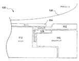
多くのプラズマ処理チャンバー内では、エッジリングが頻繁に使用される。説明のために、図1はプラズマ処理チャンバー100の簡略化された断面図を示す。ウエハ104は、チャック112上に配置され、チャック112はプラズマ処理チャンバー内においてウエハを支持する。チャック112は加工物ホルダーとして機能し、周知のように、エッチングおよび蒸着を促進するために、RF電源により通電される。カップリングリング108は、チャック112とセラミックリング110との間に配置される。カップリングリング108の一の機能は、チャック112からエッジリング102までの電流回路を提供する。エッジリング102は、多くの機能を果たし、チャック112上にウエハ104を配置し、ウエハ自体が保護することができない基礎部品を、プラズマのイオンによって損傷を受けないように保護する。
Edge rings are frequently used in many plasma processing chambers. For purposes of illustration, FIG. 1 shows a simplified cross-sectional view of the
エッジリング112の重要な機能の一は、基盤の全面にわたって処理の均一性を保つことに関する。プラズマシース(plasma sheath)106の等電位線はチャックの端を越えて鋭く上方へカーブしていることは周知である。エッジリングが無い場合、基板端部はチャックの外端を電気的に決め、等電位線は基板端部の周辺において鋭く上方へカーブするであろう。ゆえに、基板周縁部は、基板の中心に存在するプラズマ環境とは違ったプラズマ環境下に置かれることにより、その基板の全面にわたる処理の低均一化をもたらす。
One important function of the
チャックのプラズマに面する範囲を、エッジリングおよび/または他の下部構造に電気的に拡張することにより、チャックの端部は、基板端部の外側にいくらか拡張することでプラズマに電気的に露出される。このようにして、プラズマシースの等電位線は、基板の表面全体におよびより一定の状態となり、基板表面全体にわたって、処理の均一性に貢献する。 By electrically extending the plasma facing area of the chuck to an edge ring and / or other substructure, the end of the chuck is electrically exposed to the plasma by extending it somewhat outside the substrate edge. Is done. In this way, the equipotential lines of the plasma sheath are in a more constant state across the entire surface of the substrate, contributing to process uniformity across the entire substrate surface.
しかし残念なことに、エッジリングは、そのプラズマ環境により、時間が経過するに従って磨耗する傾向にある。エッジリングが磨耗していくに従って、エッジリングの損傷部近傍のプラズマ環境は変化する。そしてプラズマの変化は、時間が経過するに従って、処理結果を変えてしまい、エッジリングが磨耗するに従って処理(プロセス)の劣化をもたらす。このことは、同じチャンバー内で同じ方法を繰り返し使用した処理でさえもあてはまる。 Unfortunately, however, the edge ring tends to wear over time due to its plasma environment. As the edge ring wears, the plasma environment near the damaged portion of the edge ring changes. The change in plasma changes the processing result as time passes, and causes deterioration of the processing (process) as the edge ring wears. This is true even for processes using the same method repeatedly in the same chamber.
時間が経過するに従って、その処理結果は、エッジリングの交換が必要となるまで劣化する。エッジリングの交換が必要な時は、基板処理は停止され、プラズマ処理チャンバーはエッジリング交換を容易にするために運転が停止される。エッジリング交換作業の間、それは数時間または数日間かかるかもしれないが、製造者はプラズマ処理システムの使用を妨げられ、それはプラズマ処理システムを所有するコストをさらに増大させてしまう。 As time passes, the processing results degrade until the edge ring needs to be replaced. When the edge ring needs to be replaced, the substrate processing is stopped and the plasma processing chamber is shut down to facilitate the edge ring replacement. While it may take hours or days during an edge ring replacement operation, the manufacturer is prevented from using the plasma processing system, which further increases the cost of owning the plasma processing system.
上記理由から、エッジリングの交換が必要となる頻度を減らすことと同様に、エッジリングを使用するプラズマ処理システム内において、処理結果を向上するために改良された方法および装置が望まれる。 For the above reasons, improved methods and apparatus are desired to improve processing results in plasma processing systems that use edge rings, as well as reduce the frequency with which edge rings need to be replaced.
本発明は、一実施形態として、プラズマ処理システムのプラズマ処理チャンバー内において複数の基板を処理するための方法に関し、処理の間、それぞれの基盤は、チャック上に配置されるとともに、エッジリングに取り囲まれることを含む方法。プラズマ処理チャンバー内において所定の処理方法に従い、複数の基板のうち、第一の基板を処理することを含む方法。さらに、プラズマ処理チャンバー内のプラズマシースと、エッジリングを介するチャックとの間の静電容量経路に沿った静電容量の値を、所定の値に調整することを含む方法。さらに、その調整の後、プラズマ処理チャンバー内において、所定の処理方法に従い、複数の基板のうちの第二の基板を処理することを含む方法であって、前記調整は、エッジリングの交換を必要としなくとも、遂行することができる方法。 The present invention, in one embodiment, relates to a method for processing a plurality of substrates in a plasma processing chamber of a plasma processing system, wherein during processing each substrate is disposed on a chuck and surrounded by an edge ring. A method comprising. A method comprising processing a first substrate among a plurality of substrates in accordance with a predetermined processing method in a plasma processing chamber. The method further includes adjusting a value of the capacitance along a capacitance path between the plasma sheath in the plasma processing chamber and the chuck via the edge ring to a predetermined value. Furthermore, after the adjustment, the method includes processing a second substrate of the plurality of substrates according to a predetermined processing method in the plasma processing chamber, wherein the adjustment requires replacement of an edge ring. A method that can be performed without it.
別の実施形態として、本発明は、複数の基板を処理するために、少なくとも一のプラズマ処理チャンバーを有するプラズマ処理システムに関する。前記プラズマ処理チャンバーは、前記処理中に基板を支持するために構成されたチャックと、外周を有するエッジリングを含む。エッジリングの外周は、チャックを取り巻き、処理の間、エッジリングは、プラズマシースとチャックとの間の静電容量経路に沿って配置され、処理の間、プラズマシースは発生したプラズマと連係(associated with)する。さらに、プラズマ処理チャンバーは、静電容量経路に沿って配置された静電容量の値をその場で調整する機構を含む。 In another embodiment, the present invention relates to a plasma processing system having at least one plasma processing chamber for processing a plurality of substrates. The plasma processing chamber includes a chuck configured to support a substrate during the processing and an edge ring having an outer periphery. The outer periphery of the edge ring surrounds the chuck, and during processing, the edge ring is placed along a capacitive path between the plasma sheath and the chuck, and during processing, the plasma sheath is associated with the generated plasma. with). Further, the plasma processing chamber includes a mechanism for adjusting the value of the capacitance disposed along the capacitance path in situ.
さらに別の実施形態として、本発明は、複数の基板を処理する少なくとも一のプラズマ処理チャンバーを有するプラズマ処理システムに関する。プラズマ処理チャンバーは、処理中に基板を支持する支持手段を含む。さらに、外周を有するエッジリングを含み、そのエッジリングの外周は支持手段を取り囲み、エッジリングは、処理の間、プラズマシースと支持手段の間の静電容量経路に沿って配置され、プラズマシースは、処理の間、発生したプラズマと連係することを含む。さらに、静電容量経路に沿って配置された静電容量の値をその場で調整することを含む。 In yet another embodiment, the present invention relates to a plasma processing system having at least one plasma processing chamber for processing a plurality of substrates. The plasma processing chamber includes support means for supporting the substrate during processing. And an edge ring having an outer periphery, the outer periphery of the edge ring surrounding the support means, the edge ring being disposed along a capacitive path between the plasma sheath and the support means during processing, the plasma sheath being Interfacing with the generated plasma during processing. It further includes adjusting the value of the capacitance arranged along the capacitance path in-situ.
上記および本発明の他の特徴は、以下により詳細に、図と共に説明する。 These and other features of the present invention are described in more detail below in conjunction with the figures.
本発明は、添付の図において示されるようないくつかの実施形態を参照にして、詳細が説明される。以下の説明において、明確化された多数の詳細は、本発明の完全なる理解のために示される。本発明は、以下の明確化された詳細のいくつかが、または全てが無くても、本発明が実施される可能性があることは、同業者にとっては明白である。一方、周知の処理ステップおよび/または構造は、発明を不必要に不明確化しないためにも、詳細について説明しない。本発明の特徴と利点は、図および以下の説明によりさらに理解することができる。 The invention will now be described in detail with reference to a few embodiments as illustrated in the accompanying drawings. In the following description, numerous specific details are set forth in order to provide a thorough understanding of the present invention. It will be apparent to those skilled in the art that the present invention may be practiced without some or all of the following clarified details. In other instances, well known process steps and / or structures have not been described in detail in order not to unnecessarily obscure the invention. The features and advantages of the present invention may be further understood from the figures and the following description.
理論に縛られることを望まないが、発明者が信じることは、エッジリングが磨耗したときに、プラズマシースから、エッジリングを介するチャックまでの静電容量経路に沿う静電容量は変化するということである。そしてその静電容量の変化が、エッジリングの損傷部分近傍のプラズマ環境に影響を及ぼす。この静電容量の変化が、エッジリングが磨耗するに従って補償されないのであれば、処理プロセスの劣化は、避けられない。さらに、エッジリングが磨耗するに従って、静電容量の変化が補償されなければ、処理プロセスの劣化は修正することができず、より頻繁なエッジリングの交換を余儀なくさせる。 Without wishing to be bound by theory, the inventor believes that when the edge ring wears, the capacitance along the capacitance path from the plasma sheath to the chuck through the edge ring changes. It is. The change in capacitance affects the plasma environment near the damaged portion of the edge ring. If this change in capacitance is not compensated for as the edge ring wears, degradation of the processing process is inevitable. Furthermore, as the edge ring wears, if the change in capacitance is not compensated for, the degradation of the processing process cannot be corrected, necessitating more frequent edge ring replacement.
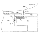
説明を容易にするために、図面2Aは、別のプラズマ処理チャンバー図を示し、それは、プラズマシース106から、エッジリング102を介するチャック112までの静電容量経路150を示す。図面2Aを参照すると、プラズマシース106、ウエハ104、チャック112、カップリングリング108、エッジリング102、セラミックリング110は、図面1に示してある。チャック112の誘導面に始まり、同等の静電容量C0が示され、その静電容量はチャック112の表面とカップリングリング108の表面、およびそれらの間のスペースにより決定される。静電容量経路150に沿って、別の同等な静電容量C2があり、それはカップリングリング108とエッジリング102の底面、およびそれらの間のスペースによって決定される。さらに、静電容量経路150に沿って、エッジリング102の誘電性の物質は、別の静電容量C1を形成する。さらに、プラズマシース106とエッジリング102の上面間の間隙は、静電容量経路150に沿って別の静電容量Csを形成する。
For ease of explanation, FIG. 2A shows another plasma processing chamber diagram, which shows a
図面2Bを参照すると、静電容量経路150のための簡略化した電気回路図が示してある。チャック112は静電容量C0に電気的に直列に接続され、そのC0はチャック112とカップリングリング108間に配置されていることを示す。静電容量C2は、カップリングリング108とエッジリング102の底面との間において、静電容量経路150に沿って直列で接続される。静電容量C1は、エッジリング102の誘電性の物質により形成され、静電容量C2に直列に接続していることを示す。静電容量Csは、静電容量C2とプラズマシース106間において、静電容量C2に直列に接続することにより、静電容量経路150を完全な状態にする。
Referring to FIG. 2B, a simplified electrical schematic for the
エッジリングが磨耗し、かつ/または、プラズマにより損傷を受けた時、エッジリングの誘電性物質に起因する静電容量C1は、変化する。静電容量C1におけるその変化はエッジリングの損傷部近傍のプラズマ環境に影響する。そのプラズマ環境が変化するに従って、処理結果は劣化する。 When the edge ring is worn and / or damaged by the plasma, the capacitance C1 due to the dielectric material of the edge ring changes. The change in capacitance C1 affects the plasma environment near the damaged portion of the edge ring. As the plasma environment changes, the processing results deteriorate.
図面3Aは、図面2Aのプラズマ処理チャンバーの簡略化した断面図を示し、エッジリング102の典型的な損傷部304を含む。損傷部304は、エッジリング102に溝、空洞、またはくぼみを作り、損傷部近傍の前述の静電容量C1を変化させると信じられる。静電容量経路の変化は、図3Bに示される。図面2Bの状況とは対照的に、静電容量C1の値は、エッジリング102の損傷した誘電性物質に起因するものであって、誘電性物質を少なくすることにより、大きくなる(C=εA/dのため)。そして静電容量C1の値の増大が、静電容量経路150に沿った全体の静電容量を増加させ、経路150に沿ったインピーダンスの減少をもたらす(Z=1/ωCまたはZ=d/εAωのため)。
3A shows a simplified cross-sectional view of the plasma processing chamber of FIG. 2A and includes a typical damaged portion 304 of the
プラズマシースからチャックまでの経路に沿ったインピーダンスが減少するに従って、経路150に沿った電流は増加する。プラズマシースと、エッジリングの損傷部を介するチャックとの間における電流の増加は、基盤の他の部分と比較して、基板端部のエッチング比の増加と一致する。さらに、基板端部のエッチングの特性は、エッジリングの侵食が進行するに従って、基板の周縁部に向かって傾斜することを示す。理想的には、基板端部のエッチング比が変化しないことであり、時間が経ってもエッチングの特性に傾斜(偏向)が起きないことである。さらに、エッジリングは、侵食されないか、後のサービスインターバルに至るまで、エッチングの効果が持続するぐらいの低速で侵食されることが理想的である。半導体製造工程はエッチング特性のわずかな変化しか許容できないので、エッジリングの寿命は、物質の単なる損傷を理由とすることよりも短くされている。本発明の目的は、基板端部のエッチング比の変化と、時間経過による傾き現象を最小限に抑えるために、エッジリングの耐用寿命を、侵食の補償によって効果的に延ばすことである。
As the impedance along the path from the plasma sheath to the chuck decreases, the current along
本発明の一の側面としては、エッジリングの損傷によるものである、静電容量経路150に沿った静電容量の変化は、静電容量C0またはC2またはCSの一以上の静電容量を減少させることによって補償される。所望の実施形態において、エッジリングの減少損失による静電容量C1の増加は、エッジリングの下面とカップリングリングとの間の間隙に連係する静電容量C2の減少によって相殺される。一実施形態において、静電容量C2の減少は、ある機構を備えることによって達成され、その機構は、エッジリングの減少損失によって起きた静電容量C1の増加を補償をするために、静電容量C2を減少させるためにそれらの間が広がるように調整することができる機構である。
In one aspect of the invention, the change in capacitance along the
本発明の一実施形態により、図4Aは、簡略化されたプラズマ処理チャンバーの断面図を、位置調整可能なカップリングリング408とともに示す。図面4Aを参照すると、位置調整可能なカップリングリング408は、経路404に沿って移動するように構成される。静電容量C2の値は、エッジリング102の下面と位置調整可能なカップリングリング408間の距離によって決まるので、位置調整可能なカップリングリング408の変更は、静電容量C2の値を変更する。
In accordance with one embodiment of the present invention, FIG. 4A shows a cross-sectional view of a simplified plasma processing chamber with an
位置調整可能なカップリングリングの使用により、損傷したエッジリング102に連係する静電容量C1の増加は、経路404に沿った位置調整可能なカップリングリング408の位置変更による静電容量C2の変更によって相殺可能である。最終結果としては、静電容量経路150に沿った静電容量全体は、実質的に均一となるか、もしくはより少ない範囲での変化となる。位置調整可能なカップリングリングの使用により、プラズマシースとチャックとの間の静電容量は、不変となるか、もしくはより少ない範囲での変化となるので、プラズマシースとチャックとの間のインピーダンスは、不変となるか、もしくはより少ない範囲での変化となる。そしてこのことは、エッジリングが磨耗していっても、エッジリングの損傷部近傍のプラズマ環境が、不変もしくはより少ない範囲で変化することを維持する助けとなる。
Due to the use of the adjustable coupling ring, the increase in capacitance C 1 associated with the damaged
さらに、位置調整可能なカップリングリングは、エッジリングの交換の必要性を遅らせる。カップリングリングは、エッジリングが磨耗するに従って、処理(プロセス)の劣化を修正するために位置変更される。しかし、甚だしい構造の損傷のためや、または、エッジリングの損傷による静電容量C1の増加は他の静電容量の一をさらに減少させることにより、ある時点をこえた場合その増加は適正に補償されないため、エッジリング102は交換を必要とする時期が来る。しかしながら、その交換は、先行技術よりも頻度は少なくなり、よって、交換プロセスによる必要な交換装置の必要性を減らすとともに、製造のコストと時間を減少させる。
In addition, the adjustable coupling ring delays the need for edge ring replacement. The coupling ring is repositioned to correct process degradation as the edge ring wears. However, the increase in capacitance C1 due to severe structural damage or due to edge ring damage can be compensated appropriately beyond a certain point in time by further decreasing one of the other capacitances. As a result, it is time to replace the
一実施形態として、エッジリングの減少した量や損傷は、時々エッジリングの厚みを測ることにより、特定のプラズマ処理チャンバー内における特定の処理のために、過去の経験から割り出すことができる。例えば、一実施形態として、影響を受けた部分におけるエッジリングの厚みは、接触検出器を使用し計測できる。一旦、時間の関数としてまたは処理された基板の数の関数として、エッジリングの減少した量が割り出されたら、時間の関数としてまたは処理された基板の数の関数として、静電容量の値C1は割り出すことができる。この情報は、エッジリング減少損失によって引き起こされた静電容量の増加を相殺するために、プラズマシースとチャックとの間の静電容量経路に沿った一以上の他の静電容量の中で、時間の関数としてまたは処理された基板の数の関数として、静電容量の必要な減少量を割り出すのに使用することができる。位置調整可能なカップリングリングの場合において、この情報は、エッジリング減少損失によって引き起こされた静電容量の増加を十分に相殺するために、時間の関数としてまたは処理された基板の数の関数として、カップリングリングとエッジリング間の、製造中に必要とされる間隙を算出するために使用することができる。 In one embodiment, the reduced amount or damage of the edge ring can be determined from past experience for a particular process within a particular plasma processing chamber, sometimes by measuring the thickness of the edge ring. For example, in one embodiment, the thickness of the edge ring at the affected part can be measured using a contact detector. Once the reduced amount of edge ring has been determined as a function of time or as a function of the number of substrates processed, the capacitance value C1 as a function of time or as a function of the number of substrates processed. Can be determined. This information, among other capacitances along the capacitance path between the plasma sheath and the chuck, to offset the capacitance increase caused by edge ring reduction loss, It can be used to determine the required reduction in capacitance as a function of time or as a function of the number of substrates processed. In the case of an adjustable coupling ring, this information can be used as a function of time or as a function of the number of substrates processed to fully offset the increase in capacitance caused by the edge ring reduction loss. Can be used to calculate the gap required during manufacturing between the coupling ring and the edge ring.
別の実施形態として、プラズマシースとチャックとの間の静電容量経路に沿った一以上の他の静電容量の減少は、プラズマ処理チャンバーのさまざまな部品の材料や、チャンバーの形状並びにその部品の形状や、処理方法などを考慮することにより、理論的に、またはコンピュータを使用したモデルによって、算出することができる。そしてこの情報は、製造チャンバー内において、プラズマシースとチャックとの間の静電容量経路に沿った一以上の他の静電容量を減少させるために使用される。 In another embodiment, one or more other capacitance reductions along the capacitive path between the plasma sheath and the chuck may be caused by the material of various parts of the plasma processing chamber, the shape of the chamber, and its parts. By taking into account the shape and processing method, it can be calculated theoretically or by a model using a computer. This information is then used to reduce one or more other capacitances along the capacitive path between the plasma sheath and the chuck within the manufacturing chamber.
プラズマシースとチャックとの間の静電容量経路に沿った一以上の他の静電容量を減少させることは、さまざまな方法において達成される。位置調整可能なカップリングリングの場合、例えば、一以上の直線型またはスクリューアクチュエータは、エッジリングに連係する位置調整可能なカップリングリング408を物理的に動かすために備えることができる。アクチュエータはチャック112またはセラミックリング110に対して、また所望されるならばエッジリング102に対しても固定することができる。
Reducing one or more other capacitances along the capacitive path between the plasma sheath and the chuck can be accomplished in various ways. In the case of an adjustable coupling ring, for example, one or more linear or screw actuators can be provided to physically move the
さらに、エッジリングは、エッジリングの減少損傷によるものである静電容量C1の増加を補償するために、交互に、または付加的に、可動するよう作られることが予期される。さらに、カップリングおよびエッジリングを静止の状態に保ち、可動の挿入物を備える事を可能にし、その可動の挿入物は、エッジリングの減少損傷によるものである静電容量C1の増加を補償するために、チャックとカップリングリング間の間隙において、またカップリングリングとエッジリング間において、またエッジリングとプラズマシース間において、必要とされるように配置される。 Furthermore, it is expected that the edge ring will be made to move alternately or additionally to compensate for the increase in capacitance C1 due to the reduced damage of the edge ring. In addition, it is possible to keep the coupling and edge ring stationary and to have a movable insert that compensates for the increase in capacitance C1, which is due to reduced damage to the edge ring. Therefore, it is arranged as required in the gap between the chuck and the coupling ring, between the coupling ring and the edge ring, and between the edge ring and the plasma sheath.
どのような場合であっても、静電容量調整はその場で遂行されることが好ましい。すなわち、プラズマシースとチャックとの間の静電容量経路に沿った一以上の他の静電容量が、長期間、製造ライン上における稼動状態からプラズマ処理チャンバーを外すことを必要とすることなしに、調整されることができるプラズマ処理チャンバーを備える機構があることが好ましい。位置調整可能なカップリングリングに接続されたアクチュエータは、エッジリングの減少損傷によるものである静電容量C1の増加を補償するための、その場で静電容量を調整する機器の種類のほんの一例である。さらなる例として、カップリングリングは、静止状態に作られることができるが、可変容量コンデンサのような調整可能なインピーダンス装置の使用により、チャックのために調整可能なインピーダンスを有することができる。この場合、この調整は、エッジリングの静電容量の変化を相殺するために必要不可欠として、調整可能なインピーダンス装置の値を調整することによって行われる。 In any case, the capacitance adjustment is preferably performed on the spot. That is, without requiring one or more other capacitances along the capacitance path between the plasma sheath and the chuck to remove the plasma processing chamber from operation on the production line for extended periods of time. Preferably, there is a mechanism comprising a plasma processing chamber that can be adjusted. The actuator connected to the adjustable coupling ring is just one example of a type of equipment that adjusts capacitance in situ to compensate for the increase in capacitance C1, which is due to reduced damage to the edge ring. It is. As a further example, the coupling ring can be made stationary, but can have an adjustable impedance for the chuck through the use of an adjustable impedance device such as a variable capacitor. In this case, this adjustment is made by adjusting the value of the adjustable impedance device as essential to offset the change in the capacitance of the edge ring.
さらに、いくつかのチャンバーの構造として、プラズマシースとエッジリングを介するチャックとの間の静電容量経路内に、より少ない、またはより多い数の部品を含むことができると理解されるべきである。含まれる部品(リングや他全ての構造など)の数に関わらず、プラズマシースとチャック本体間の静電容量経路に沿った一以上の静電容量を、エッジリングの減少損傷によるものである静電容量C1の増加を補償するために、減らすことが可能な限りは、処理(プロセス)の劣化は緩和され、そのエッジリングは、交換を必要となるまでにより長い期間使用することができる。 Furthermore, it should be understood that some chamber structures can include fewer or greater numbers of parts in the capacitive path between the plasma sheath and the chuck via the edge ring. . Regardless of the number of parts involved (rings, all other structures, etc.), one or more capacitances along the capacitance path between the plasma sheath and the chuck body will cause static damage due to reduced damage to the edge ring. As long as it can be reduced to compensate for the increase in capacitance C1, process degradation is mitigated and the edge ring can be used for a longer period of time before it needs to be replaced.
本発明がいくつかの好ましい実施形態に関して説明される一方、変更、置換、ならびに本発明の範囲内にあてはまる同等のものがある。例えば、図面は、エッチング用途の状況において示されるが、本発明は、蒸着処理にも適用されると理解されるべきである。蒸着処理の場合、または特定のエッチング処理の場合においてさえ、エッジリング上での物質の蒸着は、プラズマシースとチャック本体間の前述の静電容量経路に沿うエッジリングの静電容量を減少させることが可能であり、場合によっては、静電容量経路に沿う他の静電容量を、補償のために増加させる調整を必要とする。この場合、時間の経過に従って蒸着の量は、蒸着によるエッジリングの静電容量の変化を把握するために、過去の経験から決定することができ、エッジリングの静電容量の変化は、モデルとして作られ、数学的に算出される。そしてこの情報は、前述の静電容量経路に沿った一以上の静電容量を調整することによって、補償を促進するために使用されることが可能である。 While the invention has been described with reference to several preferred embodiments, there are alterations, substitutions, and equivalents that fall within the scope of the invention. For example, although the drawings are shown in the context of etching applications, it should be understood that the present invention also applies to vapor deposition processes. In the case of a deposition process, or even in the case of a specific etching process, the deposition of material on the edge ring reduces the edge ring capacitance along the aforementioned capacitive path between the plasma sheath and the chuck body. Is possible, and may require adjustment to increase other capacitances along the capacitance path for compensation. In this case, the amount of vapor deposition over time can be determined from past experience to grasp the change in edge ring capacitance due to vapor deposition, the change in edge ring capacitance as a model Created and mathematically calculated. This information can then be used to facilitate compensation by adjusting one or more capacitances along the aforementioned capacitance path.
さらに、本発明をいかなる特定のプラズマ発生技術の型に制限することは必要とされない。従って、本発明は、エッジリングの減少損傷またはエッジリング上の物質の増加によって、処理(プロセス)の劣化を経験する全てのプラズマ処理システムに適用することが予期され、プラズマがどのようにして生成されるかには係りなく、誘導的に接続されたプラズマ処理システムと、静電容量的に接続されたプラズマ処理システムと、他のものを含む。本発明の方法と装置を組み込む多数の別の方法があることを理解しなくてはならない。それゆえ、以下にある請求項は、本発明の意図する主旨と範囲内にあてはまる様な変更と、置換と、同等のもの全てを含むものとみなされる。 Furthermore, it is not necessary to limit the present invention to any particular type of plasma generation technology. Thus, the present invention is expected to apply to all plasma processing systems that experience process degradation due to reduced damage to the edge ring or increased material on the edge ring, and how the plasma is generated. Regardless of what is done, it includes inductively connected plasma processing systems, capacitively connected plasma processing systems, and others. It should be understood that there are many alternative ways of incorporating the method and apparatus of the present invention. Therefore, the following claims are considered to include all modifications, substitutions, and equivalents that fall within the intended spirit and scope of the present invention.
本発明は、添付された図の中に、制限するものとしてではなく例として説明され、参照番号は類似する要素を示す。 The present invention is illustrated by way of example and not limitation in the accompanying figures, where like reference numbers indicate similar elements.
Claims (27)
前記プラズマチャンバー内において所定の処理方法に従い前記複数の基板の第一の基板を処理することと、
前記プラズマ処理チャンバー内のプラズマシースと、前記チャックとの間における静電容量経路に沿った静電容量の値を調整するために、軸に沿って前記カップリングリングを移動することと、
ここで、前記静電容量経路は前記エッジリングを通過しており、前記軸は前記エッジリングの表面に対して垂直であり、前記カップリングリングを移動する工程は、前記静電容量経路に沿って少なくとも二つの隣接する表面間の間隙を増加させるものであり、
前記カップリングリングを移動する前記工程後、前記プラズマ処理チャンバー内において前記所定の処理方法に従い、前記複数の基板の第二の基板を処理することと、を含み、
前記カップリングリングを移動する前記工程は、前記静電容量経路に沿った静電容量の増加を相殺するために静電容量の値を調整するものであり、その静電容量の増加は、前記エッジリングの減少損傷によるものであることを特徴とする方法。A method of processing a plurality of substrates within a plasma processing chamber of a plasma processing system, each of the substrates being disposed on a chuck and surrounded by an edge ring during the processing, wherein the plasma The processing chamber has a coupling ring disposed between the edge ring and at least a portion of the chuck to provide a current path between the chuck and the edge ring;
Processing a first substrate of the plurality of substrates according to a predetermined processing method in the plasma chamber;
Moving the coupling ring along an axis to adjust the value of capacitance along a capacitance path between the plasma sheath in the plasma processing chamber and the chuck;
Here, the capacitance path passes through the edge ring, the axis is perpendicular to the surface of the edge ring, and the step of moving the coupling ring is along the capacitance path. Increasing the gap between at least two adjacent surfaces,
After the step of moving the coupling ring, processing a second substrate of the plurality of substrates according to the predetermined processing method in the plasma processing chamber;
The step of moving the coupling ring adjusts the value of the capacitance to offset the increase in capacitance along the capacitance path, and the increase in capacitance is A method characterized by reduced damage on the edge ring.
前記処理の間、基板を支持するために形成されたチャックと、
外周を有するエッジリングと、
ここで、前記エッジリングの前記外周は、前記チャックを取り囲み、前記エッジリングは、前記処理の間、プラズマシースと前記チャックとの間の静電容量経路に沿って配置され、前記プラズマシースは、前記処理の間、発生したプラズマに連係するものであり、
前記チャックと前記エッジリングとの間に電流路を提供するために前記エッジリングと前記チャックの少なくとも一部との間に配置されるカップリングリングと、
を有しており、前記カップリングリングは前記静電容量経路に沿って配置され、前記カップリングリングは前記カップリングリングと前記エッジリングとの間の静電容量を調整するために軸に沿って移動可能であり、前記軸は前記エッジリングの表面に対して垂直であり、前記静電容量は、所定の値だけ減少され、前記所定値は、前記静電容量性の経路に沿った静電容量の増加を相殺するのに十分な静電容量の値であり、前記静電容量の増加は、前記エッジリングの減少損傷によるものであることを特徴とするプラズマ処理システム。A plasma processing system having at least one plasma processing chamber for processing a plurality of substrates,
A chuck formed to support the substrate during the process;
An edge ring having an outer periphery;
Here, the outer periphery of the edge ring surrounds the chuck, and the edge ring is disposed along a capacitance path between the plasma sheath and the chuck during the processing, Linked to the plasma generated during the process,
A coupling ring disposed between the edge ring and at least a portion of the chuck to provide a current path between the chuck and the edge ring;
And the coupling ring is disposed along the capacitance path, the coupling ring being along an axis to adjust a capacitance between the coupling ring and the edge ring. And the axis is perpendicular to the surface of the edge ring, the capacitance is reduced by a predetermined value, and the predetermined value is a static along the capacitive path. A plasma processing system having a capacitance value sufficient to offset an increase in capacitance, wherein the increase in capacitance is due to reduced damage to the edge ring.
前記カップリングを移動するためのアクチュエータと、
をさらに含んでおり、前記カップリングリングは前記チャックと前記セラミックリングとの間で移動可能であり、前記アクチュエータは前記セラミックリングに対して固定されていることを特徴とする請求項18記載のプラズマ処理システム。Ceramic ring,
An actuator for moving the coupling;
The plasma of claim 18, further comprising: the coupling ring being movable between the chuck and the ceramic ring, and the actuator being fixed relative to the ceramic ring. Processing system.
Applications Claiming Priority (3)
| Application Number | Priority Date | Filing Date | Title |
|---|---|---|---|
| US10/247,812 | 2002-09-18 | ||
| US10/247,812 US6896765B2 (en) | 2002-09-18 | 2002-09-18 | Method and apparatus for the compensation of edge ring wear in a plasma processing chamber |
| PCT/US2003/029309 WO2004027816A2 (en) | 2002-09-18 | 2003-09-16 | A method and apparatus for the compensation of edge ring wear in a plasma processing chamber |
Publications (2)
| Publication Number | Publication Date |
|---|---|
| JP2005539397A JP2005539397A (en) | 2005-12-22 |
| JP4841840B2 true JP4841840B2 (en) | 2011-12-21 |
Family
ID=31992568
Family Applications (1)
| Application Number | Title | Priority Date | Filing Date |
|---|---|---|---|
| JP2004537951A Expired - Lifetime JP4841840B2 (en) | 2002-09-18 | 2003-09-16 | Method and apparatus for compensation of edge ring wear in a plasma processing chamber |
Country Status (11)
| Country | Link |
|---|---|
| US (2) | US6896765B2 (en) |
| EP (1) | EP1540695B1 (en) |
| JP (1) | JP4841840B2 (en) |
| KR (1) | KR101075048B1 (en) |
| CN (1) | CN100481307C (en) |
| AT (1) | ATE459975T1 (en) |
| AU (1) | AU2003276895A1 (en) |
| DE (1) | DE60331557D1 (en) |
| IL (1) | IL167491A (en) |
| TW (1) | TWI324809B (en) |
| WO (1) | WO2004027816A2 (en) |
Families Citing this family (81)
| Publication number | Priority date | Publication date | Assignee | Title |
|---|---|---|---|---|
| TW200416801A (en) * | 2003-01-07 | 2004-09-01 | Tokyo Electron Ltd | Plasma processing apparatus and focus ring |
| US7658816B2 (en) * | 2003-09-05 | 2010-02-09 | Tokyo Electron Limited | Focus ring and plasma processing apparatus |
| US7244336B2 (en) * | 2003-12-17 | 2007-07-17 | Lam Research Corporation | Temperature controlled hot edge ring assembly for reducing plasma reactor etch rate drift |
| KR100610010B1 (en) * | 2004-07-20 | 2006-08-08 | 삼성전자주식회사 | Apparatus for |
| JP4566789B2 (en) * | 2005-03-07 | 2010-10-20 | 株式会社日立ハイテクノロジーズ | Plasma processing method and plasma processing apparatus |
| JP2007250967A (en) * | 2006-03-17 | 2007-09-27 | Tokyo Electron Ltd | Plasma treating apparatus and method, and focus ring |
| JP5069452B2 (en) | 2006-04-27 | 2012-11-07 | アプライド マテリアルズ インコーポレイテッド | Substrate support with electrostatic chuck having dual temperature zones |
| US7572737B1 (en) * | 2006-06-30 | 2009-08-11 | Lam Research Corporation | Apparatus and methods for adjusting an edge ring potential substrate processing |
| US7943007B2 (en) | 2007-01-26 | 2011-05-17 | Lam Research Corporation | Configurable bevel etcher |
| JP5317424B2 (en) * | 2007-03-28 | 2013-10-16 | 東京エレクトロン株式会社 | Plasma processing equipment |
| JP4988402B2 (en) * | 2007-03-30 | 2012-08-01 | 株式会社日立ハイテクノロジーズ | Plasma processing equipment |
| US8563619B2 (en) * | 2007-06-28 | 2013-10-22 | Lam Research Corporation | Methods and arrangements for plasma processing system with tunable capacitance |
| US7837827B2 (en) * | 2007-06-28 | 2010-11-23 | Lam Research Corporation | Edge ring arrangements for substrate processing |
| US20090025636A1 (en) * | 2007-07-27 | 2009-01-29 | Applied Materials, Inc. | High profile minimum contact process kit for hdp-cvd application |
| US8343305B2 (en) * | 2007-09-04 | 2013-01-01 | Lam Research Corporation | Method and apparatus for diagnosing status of parts in real time in plasma processing equipment |
| CN101552182B (en) * | 2008-03-31 | 2010-11-03 | 北京北方微电子基地设备工艺研究中心有限责任公司 | Marginal ring mechanism used in semiconductor manufacture technology |
| US20090261065A1 (en) * | 2008-04-18 | 2009-10-22 | Lam Research Corporation | Components for use in a plasma chamber having reduced particle generation and method of making |
| WO2010062345A2 (en) * | 2008-10-31 | 2010-06-03 | Lam Research Corporation | Lower electrode assembly of plasma processing chamber |
| CN102341902A (en) * | 2009-03-03 | 2012-02-01 | 东京毅力科创株式会社 | Placing table structure, film forming apparatus, and raw material recovery method |
| JP5350043B2 (en) * | 2009-03-31 | 2013-11-27 | 東京エレクトロン株式会社 | Plasma processing apparatus and plasma processing method |
| US20110011534A1 (en) * | 2009-07-17 | 2011-01-20 | Rajinder Dhindsa | Apparatus for adjusting an edge ring potential during substrate processing |
| DE202010014805U1 (en) * | 2009-11-02 | 2011-02-17 | Lam Research Corporation (Delaware Corporation) | Hot edge ring with inclined upper surface |
| WO2011065965A2 (en) * | 2009-11-30 | 2011-06-03 | Lam Research Corporation | An electrostatic chuck with an angled sidewall |
| JP5654297B2 (en) | 2010-09-14 | 2015-01-14 | 東京エレクトロン株式会社 | Plasma processing apparatus and plasma processing method |
| JP5741124B2 (en) * | 2011-03-29 | 2015-07-01 | 東京エレクトロン株式会社 | Plasma processing equipment |
| CN103177925B (en) * | 2011-12-23 | 2015-08-26 | 中微半导体设备(上海)有限公司 | A kind of adjustable confinement ring for plasma processing apparatus |
| CN103187234B (en) * | 2011-12-30 | 2016-03-16 | 中微半导体设备(上海)有限公司 | A kind of adjustable constraint device for plasma processing apparatus |
| US8525069B1 (en) * | 2012-05-18 | 2013-09-03 | Hypertherm, Inc. | Method and apparatus for improved cutting life of a plasma arc torch |
| US20140034242A1 (en) * | 2012-07-31 | 2014-02-06 | Lam Research Corporation | Edge ring assembly for plasma processing chamber and method of manufacture thereof |
| CN106415779B (en) * | 2013-12-17 | 2020-01-21 | 东京毅力科创株式会社 | System and method for controlling plasma density |
| US10804081B2 (en) | 2013-12-20 | 2020-10-13 | Lam Research Corporation | Edge ring dimensioned to extend lifetime of elastomer seal in a plasma processing chamber |
| JP5767373B2 (en) * | 2014-07-29 | 2015-08-19 | 東京エレクトロン株式会社 | Plasma processing apparatus, plasma processing method, and storage medium for storing program for implementing the same |
| US9873180B2 (en) | 2014-10-17 | 2018-01-23 | Applied Materials, Inc. | CMP pad construction with composite material properties using additive manufacturing processes |
| US10875153B2 (en) | 2014-10-17 | 2020-12-29 | Applied Materials, Inc. | Advanced polishing pad materials and formulations |
| CN113579992A (en) | 2014-10-17 | 2021-11-02 | 应用材料公司 | CMP pad construction with composite material properties using additive manufacturing process |
| US11745302B2 (en) | 2014-10-17 | 2023-09-05 | Applied Materials, Inc. | Methods and precursor formulations for forming advanced polishing pads by use of an additive manufacturing process |
| US10658222B2 (en) * | 2015-01-16 | 2020-05-19 | Lam Research Corporation | Moveable edge coupling ring for edge process control during semiconductor wafer processing |
| US11605546B2 (en) | 2015-01-16 | 2023-03-14 | Lam Research Corporation | Moveable edge coupling ring for edge process control during semiconductor wafer processing |
| US10957561B2 (en) | 2015-07-30 | 2021-03-23 | Lam Research Corporation | Gas delivery system |
| US10854492B2 (en) * | 2015-08-18 | 2020-12-01 | Lam Research Corporation | Edge ring assembly for improving feature profile tilting at extreme edge of wafer |
| CN105185732A (en) * | 2015-08-24 | 2015-12-23 | 沈阳拓荆科技有限公司 | Ceramic ring capable of changing shape and appearance of surface film of wafer |
| US10825659B2 (en) | 2016-01-07 | 2020-11-03 | Lam Research Corporation | Substrate processing chamber including multiple gas injection points and dual injector |
| US10391605B2 (en) | 2016-01-19 | 2019-08-27 | Applied Materials, Inc. | Method and apparatus for forming porous advanced polishing pads using an additive manufacturing process |
| US10685862B2 (en) * | 2016-01-22 | 2020-06-16 | Applied Materials, Inc. | Controlling the RF amplitude of an edge ring of a capacitively coupled plasma process device |
| KR20180099776A (en) | 2016-01-26 | 2018-09-05 | 어플라이드 머티어리얼스, 인코포레이티드 | Wafer edge ring lifting solution |
| US10651015B2 (en) | 2016-02-12 | 2020-05-12 | Lam Research Corporation | Variable depth edge ring for etch uniformity control |
| US10699878B2 (en) | 2016-02-12 | 2020-06-30 | Lam Research Corporation | Chamber member of a plasma source and pedestal with radially outward positioned lift pins for translation of a substrate c-ring |
| US10438833B2 (en) | 2016-02-16 | 2019-10-08 | Lam Research Corporation | Wafer lift ring system for wafer transfer |
| US10312121B2 (en) | 2016-03-29 | 2019-06-04 | Lam Research Corporation | Systems and methods for aligning measurement device in substrate processing systems |
| US11011353B2 (en) | 2016-03-29 | 2021-05-18 | Lam Research Corporation | Systems and methods for performing edge ring characterization |
| US9852889B1 (en) * | 2016-06-22 | 2017-12-26 | Lam Research Corporation | Systems and methods for controlling directionality of ions in an edge region by using an electrode within a coupling ring |
| JP2018006299A (en) | 2016-07-08 | 2018-01-11 | 東芝メモリ株式会社 | Processing object susceptor for plasma processing apparatus, plasma processing apparatus and plasma processing method |
| CN107644802B (en) * | 2016-07-21 | 2019-09-06 | 中微半导体设备(上海)股份有限公司 | Plasma etching apparatus and its edge ring assembly and electrostatic chuck |
| US10410832B2 (en) | 2016-08-19 | 2019-09-10 | Lam Research Corporation | Control of on-wafer CD uniformity with movable edge ring and gas injection adjustment |
| US9947517B1 (en) | 2016-12-16 | 2018-04-17 | Applied Materials, Inc. | Adjustable extended electrode for edge uniformity control |
| KR102581226B1 (en) | 2016-12-23 | 2023-09-20 | 삼성전자주식회사 | Plasma processing device |
| US10553404B2 (en) | 2017-02-01 | 2020-02-04 | Applied Materials, Inc. | Adjustable extended electrode for edge uniformity control |
| US11471999B2 (en) | 2017-07-26 | 2022-10-18 | Applied Materials, Inc. | Integrated abrasive polishing pads and manufacturing methods |
| JP6974088B2 (en) * | 2017-09-15 | 2021-12-01 | 東京エレクトロン株式会社 | Plasma processing equipment and plasma processing method |
| US11075105B2 (en) | 2017-09-21 | 2021-07-27 | Applied Materials, Inc. | In-situ apparatus for semiconductor process module |
| CN109920716B (en) * | 2017-12-13 | 2021-06-08 | 中微半导体设备(上海)股份有限公司 | Plasma processing device and method for balancing etching rate |
| JP7101778B2 (en) * | 2017-12-15 | 2022-07-15 | ラム リサーチ コーポレーション | Ring structures and systems for use in plasma chambers |
| US11043400B2 (en) | 2017-12-21 | 2021-06-22 | Applied Materials, Inc. | Movable and removable process kit |
| JP7055040B2 (en) | 2018-03-07 | 2022-04-15 | 東京エレクトロン株式会社 | Placement device and processing device for the object to be processed |
| KR101995760B1 (en) * | 2018-04-02 | 2019-07-03 | 세메스 주식회사 | Apparatus and method for treating substrate |
| US10790123B2 (en) | 2018-05-28 | 2020-09-29 | Applied Materials, Inc. | Process kit with adjustable tuning ring for edge uniformity control |
| US11935773B2 (en) | 2018-06-14 | 2024-03-19 | Applied Materials, Inc. | Calibration jig and calibration method |
| WO2020050932A1 (en) | 2018-09-04 | 2020-03-12 | Applied Materials, Inc. | Formulations for advanced polishing pads |
| US11289310B2 (en) | 2018-11-21 | 2022-03-29 | Applied Materials, Inc. | Circuits for edge ring control in shaped DC pulsed plasma process device |
| US11512393B2 (en) * | 2018-11-29 | 2022-11-29 | Lam Research Corporation | Dynamic sheath control with edge ring lift |
| US10903050B2 (en) * | 2018-12-10 | 2021-01-26 | Lam Research Corporation | Endpoint sensor based control including adjustment of an edge ring parameter for each substrate processed to maintain etch rate uniformity |
| US11955314B2 (en) * | 2019-01-09 | 2024-04-09 | Tokyo Electron Limited | Plasma processing apparatus |
| US11101115B2 (en) | 2019-04-19 | 2021-08-24 | Applied Materials, Inc. | Ring removal from processing chamber |
| KR102214333B1 (en) | 2019-06-27 | 2021-02-10 | 세메스 주식회사 | Apparatus and method for treating substrate |
| JP7278160B2 (en) * | 2019-07-01 | 2023-05-19 | 東京エレクトロン株式会社 | Etching method and plasma processing apparatus |
| US20220285136A1 (en) * | 2019-08-05 | 2022-09-08 | Lam Research Corporation | Edge ring systems for substrate processing systems |
| CN112885690B (en) * | 2019-11-29 | 2023-10-20 | 中微半导体设备(上海)股份有限公司 | Plasma processing device |
| US11380575B2 (en) | 2020-07-27 | 2022-07-05 | Applied Materials, Inc. | Film thickness uniformity improvement using edge ring and bias electrode geometry |
| CN112259452B (en) * | 2020-10-21 | 2023-04-07 | 上海华力集成电路制造有限公司 | Control method of plasma dry etching process |
| KR102587757B1 (en) | 2021-01-20 | 2023-10-12 | 주식회사 레인테크 | Attaching apparatus and attaching method |
| KR102335630B1 (en) | 2021-04-20 | 2021-12-08 | (주)앤피에스 | Heat source device, substrate support device and substrate processing facility |
Citations (6)
| Publication number | Priority date | Publication date | Assignee | Title |
|---|---|---|---|---|
| WO1998039500A1 (en) * | 1997-03-07 | 1998-09-11 | Tokyo Electron Limited | Plasma etching device |
| WO1999033087A1 (en) * | 1997-12-19 | 1999-07-01 | Lam Research Corporation | Focus rings and methods therefor |
| WO1999064644A1 (en) * | 1998-06-10 | 1999-12-16 | Lam Research Corporation | Ion energy attenuation |
| WO2001050497A1 (en) * | 1999-12-30 | 2001-07-12 | Lam Research Corporation | Electrode assembly |
| WO2002025695A2 (en) * | 2000-09-18 | 2002-03-28 | Tokyo Electron Limited | Tunable focus ring for plasma processing |
| JP2002176030A (en) * | 2000-12-07 | 2002-06-21 | Semiconductor Leading Edge Technologies Inc | System and method for plasma etching |
Family Cites Families (4)
| Publication number | Priority date | Publication date | Assignee | Title |
|---|---|---|---|---|
| JPH04110653A (en) * | 1990-08-31 | 1992-04-13 | Hitachi Ltd | Method for analyzing gas sample using plasma |
| US6074488A (en) * | 1997-09-16 | 2000-06-13 | Applied Materials, Inc | Plasma chamber support having an electrically coupled collar ring |
| US6528751B1 (en) * | 2000-03-17 | 2003-03-04 | Applied Materials, Inc. | Plasma reactor with overhead RF electrode tuned to the plasma |
| US6475336B1 (en) * | 2000-10-06 | 2002-11-05 | Lam Research Corporation | Electrostatically clamped edge ring for plasma processing |
-
2002
- 2002-09-18 US US10/247,812 patent/US6896765B2/en not_active Expired - Lifetime
-
2003
- 2003-09-16 EP EP03797912A patent/EP1540695B1/en not_active Expired - Lifetime
- 2003-09-16 CN CNB038223147A patent/CN100481307C/en not_active Expired - Lifetime
- 2003-09-16 DE DE60331557T patent/DE60331557D1/en not_active Expired - Lifetime
- 2003-09-16 AT AT03797912T patent/ATE459975T1/en not_active IP Right Cessation
- 2003-09-16 KR KR1020057004768A patent/KR101075048B1/en active IP Right Grant
- 2003-09-16 WO PCT/US2003/029309 patent/WO2004027816A2/en active Application Filing
- 2003-09-16 JP JP2004537951A patent/JP4841840B2/en not_active Expired - Lifetime
- 2003-09-16 AU AU2003276895A patent/AU2003276895A1/en not_active Abandoned
- 2003-09-18 TW TW092125775A patent/TWI324809B/en not_active IP Right Cessation
-
2004
- 2004-10-22 US US10/971,971 patent/US7176403B2/en not_active Expired - Lifetime
-
2005
- 2005-03-16 IL IL167491A patent/IL167491A/en not_active IP Right Cessation
Patent Citations (6)
| Publication number | Priority date | Publication date | Assignee | Title |
|---|---|---|---|---|
| WO1998039500A1 (en) * | 1997-03-07 | 1998-09-11 | Tokyo Electron Limited | Plasma etching device |
| WO1999033087A1 (en) * | 1997-12-19 | 1999-07-01 | Lam Research Corporation | Focus rings and methods therefor |
| WO1999064644A1 (en) * | 1998-06-10 | 1999-12-16 | Lam Research Corporation | Ion energy attenuation |
| WO2001050497A1 (en) * | 1999-12-30 | 2001-07-12 | Lam Research Corporation | Electrode assembly |
| WO2002025695A2 (en) * | 2000-09-18 | 2002-03-28 | Tokyo Electron Limited | Tunable focus ring for plasma processing |
| JP2002176030A (en) * | 2000-12-07 | 2002-06-21 | Semiconductor Leading Edge Technologies Inc | System and method for plasma etching |
Also Published As
| Publication number | Publication date |
|---|---|
| WO2004027816A2 (en) | 2004-04-01 |
| IL167491A (en) | 2009-08-03 |
| US20050056622A1 (en) | 2005-03-17 |
| KR101075048B1 (en) | 2011-10-19 |
| WO2004027816A3 (en) | 2004-12-09 |
| CN100481307C (en) | 2009-04-22 |
| KR20050050660A (en) | 2005-05-31 |
| TW200408043A (en) | 2004-05-16 |
| EP1540695B1 (en) | 2010-03-03 |
| DE60331557D1 (en) | 2010-04-15 |
| US6896765B2 (en) | 2005-05-24 |
| TWI324809B (en) | 2010-05-11 |
| CN1682344A (en) | 2005-10-12 |
| AU2003276895A1 (en) | 2004-04-08 |
| US7176403B2 (en) | 2007-02-13 |
| US20040053428A1 (en) | 2004-03-18 |
| JP2005539397A (en) | 2005-12-22 |
| EP1540695A2 (en) | 2005-06-15 |
| ATE459975T1 (en) | 2010-03-15 |
Similar Documents
| Publication | Publication Date | Title |
|---|---|---|
| JP4841840B2 (en) | Method and apparatus for compensation of edge ring wear in a plasma processing chamber | |
| CN108369922B (en) | Wafer edge ring lifting solution | |
| KR102496625B1 (en) | Tunable upper plasma-exclusion-zone ring for a bevel etcher | |
| CN106997842B (en) | Controlling RF amplitude of an edge ring of capacitively coupled plasma processing apparatus | |
| KR100938635B1 (en) | Plasma confinement baffle and flow equalizer for enhanced magnetic control of plasma radial distribution | |
| TWI747837B (en) | Edge ring assembly for plasma processing chamber and system for plasma processing | |
| KR100900585B1 (en) | Focus ring and plasma processing apparatus | |
| US20210082733A1 (en) | Mounting table and plasma processing apparatus | |
| US8426317B2 (en) | Plasma processing apparatus and plasma processing method | |
| JP5597456B2 (en) | Dielectric thickness setting method and substrate processing apparatus provided with dielectric provided on electrode | |
| KR20190118974A (en) | Plasma processing apparatus, plasma control method, computer readable recording medium | |
| US10170284B2 (en) | Plasma processing method and plasma processing apparatus | |
| JP7185725B2 (en) | Wafer Edge Ring Lifting Solution | |
| US20200234928A1 (en) | Semiconductor plasma processing equipment with wafer edge plasma sheath tuning ability | |
| US20100043975A1 (en) | Movable gas introduction structure and substrate processing apparatus having same | |
| KR20080102926A (en) | Semiconductor apparatus and method using the same | |
| KR101756853B1 (en) | Substrate processing method and substrate processing apparatus | |
| JP5305287B2 (en) | Semiconductor manufacturing equipment | |
| US20220359169A1 (en) | Apparatus for fabricating a semiconductor structure and method of fabricating a semiconductor structure | |
| US10923333B2 (en) | Substrate processing apparatus and substrate processing control method |
Legal Events
| Date | Code | Title | Description |
|---|---|---|---|
| A621 | Written request for application examination |
Free format text: JAPANESE INTERMEDIATE CODE: A621 Effective date: 20060824 |
|
| A131 | Notification of reasons for refusal |
Free format text: JAPANESE INTERMEDIATE CODE: A131 Effective date: 20091027 |
|
| A601 | Written request for extension of time |
Free format text: JAPANESE INTERMEDIATE CODE: A601 Effective date: 20100127 |
|
| A602 | Written permission of extension of time |
Free format text: JAPANESE INTERMEDIATE CODE: A602 Effective date: 20100203 |
|
| A521 | Request for written amendment filed |
Free format text: JAPANESE INTERMEDIATE CODE: A523 Effective date: 20100222 |
|
| A131 | Notification of reasons for refusal |
Free format text: JAPANESE INTERMEDIATE CODE: A131 Effective date: 20101126 |
|
| A521 | Request for written amendment filed |
Free format text: JAPANESE INTERMEDIATE CODE: A523 Effective date: 20110207 |
|
| A131 | Notification of reasons for refusal |
Free format text: JAPANESE INTERMEDIATE CODE: A131 Effective date: 20110315 |
|
| A601 | Written request for extension of time |
Free format text: JAPANESE INTERMEDIATE CODE: A601 Effective date: 20110613 |
|
| A602 | Written permission of extension of time |
Free format text: JAPANESE INTERMEDIATE CODE: A602 Effective date: 20110620 |
|
| A601 | Written request for extension of time |
Free format text: JAPANESE INTERMEDIATE CODE: A601 Effective date: 20110706 |
|
| A602 | Written permission of extension of time |
Free format text: JAPANESE INTERMEDIATE CODE: A602 Effective date: 20110714 |
|
| A521 | Request for written amendment filed |
Free format text: JAPANESE INTERMEDIATE CODE: A523 Effective date: 20110809 |
|
| TRDD | Decision of grant or rejection written | ||
| A01 | Written decision to grant a patent or to grant a registration (utility model) |
Free format text: JAPANESE INTERMEDIATE CODE: A01 Effective date: 20110906 |
|
| A01 | Written decision to grant a patent or to grant a registration (utility model) |
Free format text: JAPANESE INTERMEDIATE CODE: A01 |
|
| A61 | First payment of annual fees (during grant procedure) |
Free format text: JAPANESE INTERMEDIATE CODE: A61 Effective date: 20111005 |
|
| R150 | Certificate of patent or registration of utility model |
Ref document number: 4841840 Country of ref document: JP Free format text: JAPANESE INTERMEDIATE CODE: R150 Free format text: JAPANESE INTERMEDIATE CODE: R150 |
|
| FPAY | Renewal fee payment (event date is renewal date of database) |
Free format text: PAYMENT UNTIL: 20141014 Year of fee payment: 3 |
|
| R250 | Receipt of annual fees |
Free format text: JAPANESE INTERMEDIATE CODE: R250 |
|
| RD02 | Notification of acceptance of power of attorney |
Free format text: JAPANESE INTERMEDIATE CODE: R3D02 |
|
| R250 | Receipt of annual fees |
Free format text: JAPANESE INTERMEDIATE CODE: R250 |
|
| R250 | Receipt of annual fees |
Free format text: JAPANESE INTERMEDIATE CODE: R250 |
|
| R250 | Receipt of annual fees |
Free format text: JAPANESE INTERMEDIATE CODE: R250 |
|
| R250 | Receipt of annual fees |
Free format text: JAPANESE INTERMEDIATE CODE: R250 |
|
| R250 | Receipt of annual fees |
Free format text: JAPANESE INTERMEDIATE CODE: R250 |
|
| R250 | Receipt of annual fees |
Free format text: JAPANESE INTERMEDIATE CODE: R250 |
|
| R250 | Receipt of annual fees |
Free format text: JAPANESE INTERMEDIATE CODE: R250 |
|
| R250 | Receipt of annual fees |
Free format text: JAPANESE INTERMEDIATE CODE: R250 |
|
| EXPY | Cancellation because of completion of term |