JP4832835B2 - Read / write control method for nonvolatile semiconductor memory device - Google Patents
Read / write control method for nonvolatile semiconductor memory device Download PDFInfo
- Publication number
- JP4832835B2 JP4832835B2 JP2005265080A JP2005265080A JP4832835B2 JP 4832835 B2 JP4832835 B2 JP 4832835B2 JP 2005265080 A JP2005265080 A JP 2005265080A JP 2005265080 A JP2005265080 A JP 2005265080A JP 4832835 B2 JP4832835 B2 JP 4832835B2
- Authority
- JP
- Japan
- Prior art keywords
- vcc
- voltage
- circuit
- drain
- gnd
- Prior art date
- Legal status (The legal status is an assumption and is not a legal conclusion. Google has not performed a legal analysis and makes no representation as to the accuracy of the status listed.)
- Expired - Fee Related
Links
- 238000000034 method Methods 0.000 title claims description 20
- 239000004065 semiconductor Substances 0.000 title claims description 20
- 239000002784 hot electron Substances 0.000 claims description 14
- 238000003860 storage Methods 0.000 claims description 7
- 230000005641 tunneling Effects 0.000 claims description 7
- 239000000758 substrate Substances 0.000 claims description 6
- 238000010586 diagram Methods 0.000 description 13
- LPQOADBMXVRBNX-UHFFFAOYSA-N ac1ldcw0 Chemical compound Cl.C1CN(C)CCN1C1=C(F)C=C2C(=O)C(C(O)=O)=CN3CCSC1=C32 LPQOADBMXVRBNX-UHFFFAOYSA-N 0.000 description 8
- 238000002347 injection Methods 0.000 description 8
- 239000007924 injection Substances 0.000 description 8
- 230000008569 process Effects 0.000 description 6
- VYPSYNLAJGMNEJ-UHFFFAOYSA-N Silicium dioxide Chemical compound O=[Si]=O VYPSYNLAJGMNEJ-UHFFFAOYSA-N 0.000 description 5
- 230000000694 effects Effects 0.000 description 5
- 229910052814 silicon oxide Inorganic materials 0.000 description 5
- 238000012795 verification Methods 0.000 description 5
- 230000003213 activating effect Effects 0.000 description 4
- 230000004888 barrier function Effects 0.000 description 4
- 230000000644 propagated effect Effects 0.000 description 4
- 238000005516 engineering process Methods 0.000 description 3
- 239000000463 material Substances 0.000 description 3
- 230000008859 change Effects 0.000 description 2
- 230000005684 electric field Effects 0.000 description 2
- 238000000605 extraction Methods 0.000 description 2
- 230000009191 jumping Effects 0.000 description 2
- 150000004767 nitrides Chemical class 0.000 description 2
- 230000004044 response Effects 0.000 description 2
- 238000004904 shortening Methods 0.000 description 2
- 229910052581 Si3N4 Inorganic materials 0.000 description 1
- 230000004913 activation Effects 0.000 description 1
- 230000007423 decrease Effects 0.000 description 1
- 238000007599 discharging Methods 0.000 description 1
- 238000004519 manufacturing process Methods 0.000 description 1
- 239000002159 nanocrystal Substances 0.000 description 1
- 230000003071 parasitic effect Effects 0.000 description 1
- 229910021420 polycrystalline silicon Inorganic materials 0.000 description 1
- 229920005591 polysilicon Polymers 0.000 description 1
- HQVNEWCFYHHQES-UHFFFAOYSA-N silicon nitride Chemical compound N12[Si]34N5[Si]62N3[Si]51N64 HQVNEWCFYHHQES-UHFFFAOYSA-N 0.000 description 1
Images


Landscapes
- Read Only Memory (AREA)
- Semiconductor Memories (AREA)
- Non-Volatile Memory (AREA)
Description
本発明は、不揮発性半導体メモリセルのゲート長の短縮化を実現した不揮発性半導体記憶装置の読み書き制御方法に関する。 The present invention relates to a read / write control method for a nonvolatile semiconductor memory device in which the gate length of a nonvolatile semiconductor memory cell is shortened.
近年、ランダムアクセス読み出しが可能な所謂コードストレージ用のNORフラッシュメモリのスケーリングの限界について懸念が高まってきている。 In recent years, there has been a growing concern about the limitations of scaling of a so-called code storage NOR flash memory capable of random access reading.
ITRS(InternationalTechnology Roadmap for Semiconductors) の2004年での技術予測によれば、半導体プロセス技術としては20nmプロセスの時代になっていると予測される2018年においても、NOR型フラッシュメモリのメモリセルのゲート長は130nmを実現することが困難であると指摘されている。 According to ITRS (International Technology Roadmap for Semiconductors) technology forecast in 2004, the gate length of memory cells of NOR type flash memory is expected even in 2018 when semiconductor technology is expected to be in the age of 20 nm process. It is pointed out that it is difficult to realize 130 nm.
NOR型フラッシュメモリのゲート長がスケーリングできない大きな要因の一つは、書き込み動作にチャネルホットエレクトロン(CHE)注入を用いていることにある。すなわち、チャネルホットエレクトロンを効率よく発生させるためには、メモリセルのソース−ドレイン間にトンネル絶縁膜(シリコン酸化膜)の障壁電圧以上の比較的大きな電位差が必要とされる。この電位差のためにドレインからソースに向けて比較的大きな空乏層が形成されるため、ゲート長を短くすると、ドレインからソースへ空乏層がつながってしまい(パンチスルー)、ホットエレクトロンが発生しなくなってしまうという問題があるからである。 One of the major factors that the gate length of the NOR flash memory cannot be scaled is that channel hot electron (CHE) injection is used for the write operation. That is, in order to efficiently generate channel hot electrons, a relatively large potential difference higher than the barrier voltage of the tunnel insulating film (silicon oxide film) is required between the source and drain of the memory cell. Because of this potential difference, a relatively large depletion layer is formed from the drain to the source. If the gate length is shortened, the depletion layer is connected from the drain to the source (punch-through), and hot electrons are not generated. This is because there is a problem of end.
これに対して、トンネル絶縁膜としてシリコン酸化膜よりも障壁電圧の低い材質のものを用いることでソース−ドレイン間の電位差Vdsを小さくする提案がなされている(たとえば特許文献1)。また、書き込み動作をチャネルホットエレクトロン注入以外の方式で行うNOR型フラッシュメモリも提案されている(たとえば特許文献2)。
しかしながら、特許文献1のものは、前記材質の電荷リーク特性がシリコン酸化膜に比べて劣る等の理由のために、不揮発性半導体メモリのトンネル絶縁膜として実用にいたっていない。
However, the material of
また、特許文献2のものは、チャネルホットエレクトロン注入に代えてバンド間トンネルで誘起したホットエレクトロン(BBHE)注入で書き込みを行うものであるが、この方式であっても、ホットエレクトロンのエネルギをトンネル絶縁膜の障壁電位以上にするためにはソース−ドレイン間の電位差Vdsを比較的大きな値(たとえば4V)にする必要があり、これによってゲート長の短縮化が制約をうけるという問題があった。
Further, in
そこで、この発明は、ソース−ドレイン間の電位差Vdsを小さくしてメモリセルのゲート長を短くできるようにするとともに、高速化を図った不揮発性半導体記憶装置およびその書込方法を提供することを目的とする。 SUMMARY OF THE INVENTION Accordingly, the present invention provides a nonvolatile semiconductor memory device and a writing method thereof which can reduce the potential difference Vds between the source and the drain to shorten the gate length of the memory cell and increase the speed . Objective.
半導体基板に形成されたウェルと、前記ウェルに形成されたソースおよびドレインと、
前記ソース−ドレイン間に形成されたチャンネル領域と、前記チャンネル領域の上方にトンネル絶縁膜を介して形成された電荷蓄積層と、前記電荷蓄積層の上方に絶縁膜を介して形成されたゲート電極と、を有する不揮発性半導体記憶装置のメモリセルの読み書き方法であって、
書き込み時に、電源電圧をVCCで表し、
「VP>VSB>Vs>Vd」「VSB>0V」「Vd≦VCC」
の関係を有する電圧VP、VSB、VsおよびVdを、それぞれゲート電極、ウェル電極、ソース電極およびドレイン電極に印加することにより、ドレイン付近にバンド間トンネリングによるホットエレクトロンを発生させ、このホットエレクトロンを前記電荷蓄積層に注入して前記メモリセルにビットデータの書き込みを行い、
消去に続く消去ベリファイ時に、選択ブロック内の全てのワード線に同一のベリファイ電圧を与えることを特徴とする。
A well formed in a semiconductor substrate; a source and a drain formed in the well;
A channel region formed between the source and drain; a charge storage layer formed above the channel region via a tunnel insulating film; and a gate electrode formed above the charge storage layer via an insulating film A method for reading and writing memory cells of a nonvolatile semiconductor memory device, comprising:
When writing, the power supply voltage is represented by VCC,
“VP>VSB>Vs> Vd” “VSB> 0 V” “Vd ≦ VCC”
Voltage VP to have a relationship, VSB, the Vs and Vd, respectively the gate electrodes, the well electrode, by applying to the source electrode and the drain electrode, hot electrons are generated by band-to-band tunneling in the vicinity of the drain, the hot electrons Injecting into the charge storage layer to write bit data to the memory cell,
The same verify voltage is applied to all the word lines in the selected block at the time of erase verify following the erase .
この発明によれば、書込時に「VP>VSB>Vs>Vd」「VSB>0V」「Vd≦VCC」の関係になるように設定したことにより、すなわち、ソース電圧Vsをウェル電圧VSBとドレイン電圧Vdの間の電圧にしたことにより、バンド間トンネリングによるホットエレクトロンまたはホットホールを効率よく発生させることができるとともに、ソース−ドレイン間の電位差を小さくすることができ、それにともないゲート長を短縮化できる。 According to the present invention, the relation of “VP>VSB>Vs> Vd”, “VSB> 0V”, “Vd ≦ VCC” is set at the time of writing, that is, the source voltage Vs is set to the well voltage VSB and the drain. By setting the voltage between the voltages Vd , hot electrons or hot holes can be generated efficiently by band-to-band tunneling, the potential difference between the source and drain can be reduced, and the gate length is shortened accordingly. it can.
なお、高速書込のためには、ウェル電圧VSBとドレイン電圧Vdとの電位差はトンネル絶縁膜の障壁電位と同等またはそれ以上であることが好ましい。 For high-speed writing, the potential difference between the well voltage VSB and the drain voltage Vd is preferably equal to or higher than the barrier potential of the tunnel insulating film.
また、消去に続く消去ベリファイ時に、選択ブロック内の全てにワード線に同一のベリファイ電圧を与えることによって、ブロック内の全てのメモリセルを一回の読み出しでベリファイでき、消去ベリファイの時間を短縮できる。Further, at the time of erase verify following erase, by applying the same verify voltage to the word lines for all in the selected block, all the memory cells in the block can be verified by a single read, and the erase verify time can be shortened. .
図面を参照して本発明の実施形態について説明する。
図1はこの発明が適用されるpチャンネルMONOSメモリセルの構造を示す図である。このメモリセルは、p型半導体基板11上に形成されたn型ウェル(セルウェル)12、このn型ウェル12の表面付近に所定の間隔を開けて形成されたp+領域(ソース)13およびp+領域(ドレイン)14、これら2つのp型領域13、14の間に形成されたチャネル領域20、および、このチャネル領域20の上方にチャネル領域20を覆うように形成されたONO膜およびゲート電極18を有している。
Embodiments of the present invention will be described with reference to the drawings.
FIG. 1 is a diagram showing the structure of a p-channel MONOS memory cell to which the present invention is applied. This memory cell includes an n-type well (cell well) 12 formed on a p-
ONO膜は、酸化シリコンからなるトンネル絶縁膜15、窒化シリコンからなり注入された電荷(電子)を蓄積する電荷トラップ層16、および、酸化シリコンからなる絶縁膜17からなっている。これら3層の膜厚は、トンネル絶縁膜15が約2.5〜5nm程度、電荷トラップ層16が約10nm程度、絶縁膜17が約5nm程度である。また、ゲート電極18は、ポリシリコンで構成されている。なお、ゲート長は、後述する書込電位配置により、極めて短くすることができ60nm以下が実現可能である。
The ONO film includes a
次に、図2を参照して上記pチャネルMONOSメモリセルをNOR接続のアレイ状に接続した構造の不揮発性半導体記憶装置のアーキテクチャについて説明する。
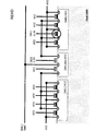
この不揮発性半導体記憶装置では、2つのセルウェル12がペアになっている。各セルウェル12には、X方向1kB=8k(8192)個×Y方向64個=512k(524288)個のメモリセルが形成されている。メインビットライン21は8k本であり、セレクトゲート24を介して2つのセルウェル12のうちの一方のサブビットライン25に接続される。8k本のメインビットライン21には、それぞれカラムラッチが接続されている。このカラムラッチは書き込み動作のベリファイ等にも用いる。セレクトゲート24は、セルウェル12とは別のセレクトゲートウェル(n型ウェル)20内に形成されており、pチャネルMOSトランジスタで構成されている。セレクトゲートウェル20の電位は通常VCC(たとえば1.8V)に設定されている。セレクトゲート24のゲート電極は、非選択時にVCCが印加され、選択時に−2.2Vが印加される。−2.2Vが印加されると、ゲートが導通し、メインビットライン21を各メモリセルのドレインにつながるサブビットライン25に接続する。ワード線は、各メモリセルのゲート電極をX方向に接続しており、各セルウェル12毎に64本設けられている。ソースラインは、各セルウェル12内の512k個のメモリセルに共通である。
Next, the architecture of a nonvolatile semiconductor memory device having a structure in which the p-channel MONOS memory cells are connected in an NOR-connected array will be described with reference to FIG.
In this nonvolatile semiconductor memory device, two
なお、電圧VCCおよび電圧GND(接地電圧)は、メモリセル外部の電源回路から供給されるものである。 The voltage VCC and the voltage GND (ground voltage) are supplied from a power supply circuit outside the memory cell.
次に、図2のNOR接続の不揮発性半導体記憶装置において、プログラム,プログラムベリファイ,消去,消去ベリファイ,読み出しを行う動作を図3〜図24を参照して説明する。
図3は各動作時に各部に印加される電圧について示している。ここで、各記号の意味は次のとおりである。
Next, in the NOR-connected non-volatile semiconductor memory device of FIG. 2, operations for performing program, program verify, erase, erase verify, and read will be described with reference to FIGS.
FIG. 3 shows the voltage applied to each part during each operation. Here, the meaning of each symbol is as follows.
MBL:メインビット線
SG:セレクトゲート
SBL:サブビット線
WL:ワード線
SL:ソース線
WEL:ウェル
WELSG:セレクトゲートのウェル
sub:基板
また、図12〜14は、上記各動作状態の変化に応じた各部の電位変化について示している。
MBL: main bit line SG: select gate SBL: sub-bit line WL: word line SL: source line WEL: well WELSG: well of select gate sub: substrate Further, FIGS. It shows the potential change of each part.
〈プログラム動作〉
図4は、プログラム動作時の電位配置および動作原理を示す図である。
この不揮発性半導体記憶装置では、BBHE注入による書き込み時に、ソース電圧Vsをセルウェル電圧VSBよりも低くしてドレイン電圧Vdに近づけ、ドレイン−ソース間の電位差を小さくしたことにより、且つ、セルウェルに適切なバックゲート電圧を印加したことによるバックゲート効果によって、等価的にしきい値電圧Vth(絶対値)を高くしたことにより、ソース−ドレイン間がパンチスルーしにくくしている。これにより、ゲート長を0.1μm以下、たとえば60nm程度まで短くしたセル構造を実現している。
<Program operation>
FIG. 4 is a diagram showing the potential arrangement and operation principle during the program operation.
In this nonvolatile semiconductor memory device, when writing by BBHE injection, the source voltage Vs is made lower than the cell well voltage VSB so as to be close to the drain voltage Vd, and the potential difference between the drain and the source is reduced. By making the threshold voltage Vth (absolute value) equivalently higher by the back gate effect due to the application of the back gate voltage, it is difficult to punch through between the source and the drain. This realizes a cell structure in which the gate length is reduced to 0.1 μm or less, for example, about 60 nm.
また、セルウェルに適切なバックゲート電圧を印加することにより、書き込みおよび読み出し時に最も高速な動作が要求されるビットラインをGND−VCCで動作させることができるようにしている。これにより、ビットラインの制御回路を高速で標準的な正のVCC回路で構成することができ、高速化かつ構成の簡略化を可能にしている。 Further, by applying an appropriate back gate voltage to the cell well, the bit line that requires the highest speed operation at the time of writing and reading can be operated by GND-VCC. As a result, the bit line control circuit can be configured with a high-speed standard positive VCC circuit, which enables high-speed and simplified configuration.
まず書き込み動作のうちのプログラム動作について説明する。先に説明したようにMONOSメモリセルでは、電荷トラップ層16として導電性が低い窒化膜を用いているため、トラップされた電子が膜内で移動せず、トラップされた位置に留まる。
メモリセルへの書き込み(プログラム)は、電荷トラップ層16へ電子を注入することによって行う。電子の注入は、図1に示したゲート電極18とドレイン14との間に正負の高電圧を印加することによるBBHE注入で行い、電子を電荷トラップ層16に注入する。
First, the program operation of the write operation will be described. As described above, in the MONOS memory cell, since the nitride film having low conductivity is used as the
Writing (programming) into the memory cell is performed by injecting electrons into the
電荷トラップ層16への電荷の注入は、正電位のゲート電極18と負電位のドレイン14の高い電位差によって生じる空乏層の高電界を利用したバンド間トンネリングによるホットエレクトロン(BBHE:Band-to-Band tunneling induced Hot Electron)注入で行う。ただし、ドレイン(=ビット線)を正電位の範囲で制御できるようにするため、セルウェル12に正のバックゲート電圧を印加する。これにより、ドレインの接地電位は相対的に負電位となる。
Charge injection into the
具体的には、図2〜図5に示すように、セルウェル12にバックゲート電圧VSBとして+4Vを印加し、ビット線BL(但し、図4の例では、セルウェルごとにビット線を区分するためにメインビット線MBLおよびセレクトゲートSGを設けているので、メインビット線MBL)を接地電位GND(=0V)とする。そして、ワード線WLにゲート電圧VPとして10Vを印加する。このときソース線SLには、VCC(=1.8V)を印加しておく。 Specifically, as shown in FIGS. 2 to 5, +4 V is applied as the back gate voltage VSB to the cell well 12, and the bit line BL (however, in the example of FIG. 4, the bit line is divided for each cell well). Since the main bit line MBL and the select gate SG are provided, the main bit line MBL) is set to the ground potential GND (= 0V). Then, 10V is applied as the gate voltage VP to the word line WL. At this time, VCC (= 1.8 V) is applied to the source line SL.
このプログラム動作を図12・図15を用いて説明する。
図15はカラムラッチの構成を示す図である。図12はプログラム動作時の図15各部の電圧波形図である。
This program operation will be described with reference to FIGS.
FIG. 15 is a diagram showing the configuration of the column latch. FIG. 12 is a voltage waveform diagram of each part of FIG. 15 during the program operation.
まず、図15に示すカラムラッチには書き込みデータが予めセットされており、書き込むべきビット線(選択MBL)に対してはノードNA=L、ノードNB=H状態(Lはローレベル、Hはハイレベルである。)であり、書き込まないビット線(非選択MBL)に対してはNA=H、NB=Lとする。 First, write data is set in advance in the column latch shown in FIG. 15. For the bit line to be written (selected MBL), node NA = L, node NB = H state (L is low level, H is high level) The bit lines (non-selected MBL) that are not written and are not written are set to NA = H and NB = L.
スタンバイ状態から、まずt1において、選択WELを4Vにする。これはWELドライバ回路にディストリビュータ回路を介して接続されている正チャージポンプ回路を活性化することで実現する。 From the standby state, first, at t1, the selection WEL is set to 4V. This is realized by activating a positive charge pump circuit connected to the WEL driver circuit via a distributor circuit.
t2において、選択SGを−2.2Vにする。これはSGドライバ回路にディストリビュータを介して接続されている負チャージポンプ回路を活性化することで実現できる。これにより選択SBLがMBLとつながりVCCに充電される。 At t2, the selection SG is set to -2.2V. This can be realized by activating a negative charge pump circuit connected to the SG driver circuit via a distributor. As a result, the selected SBL is connected to MBL and charged to VCC.
t3において、非選択WLをGNDにする。これまでは選択WLも非選択WLも共にVCCにしていた。詳細説明は別途WLドライバ回路説明時に行う。
t4において、選択WLを10Vにする。これは、WLドライバ回路にディストリビュータ回路を介して接続されている正チャージポンプ回路を活性化することで実現する。
At t3, the non-selected WL is set to GND. Until now, both selected WL and non-selected WL have been set to VCC. Detailed description will be made separately when the WL driver circuit is described.
At t4, the selection WL is set to 10V. This is realized by activating a positive charge pump circuit connected to the WL driver circuit via a distributor circuit.
t5において、/BLH=Hとし、トランジスタP9をOFFにし、MBLをHフローティング状態にする。
t6において、DDRV=H、/DDRV=Lとする。これにより、書き込むべきビット線に対してはノードNB=Hであるので、MBLはL(GNDレベル)にセットされる。一方、書き込みしないビット線に対してはNB=Lであるので、MBLはH(VCCレベル)にセットされる。
At t5, / BLH = H is set, the transistor P9 is turned off, and MBL is set in the H floating state.
At t6, DDRV = H and / DDRV = L. Thereby, for the bit line to be written, since node NB = H, MBL is set to L (GND level). On the other hand, MBL is set to H (VCC level) because NB = L for a bit line not to be written.
t7の状態で、選択メモリセルのセルウェルには4V、ドレインには0V、ゲートには10V、ソースにはVCC(=1.8V)をそれぞれ印加する。 In the state of t7, 4V is applied to the cell well of the selected memory cell, 0V is applied to the drain, 10V is applied to the gate, and VCC (= 1.8V) is applied to the source.
この電圧配置にすることにより、ドレインとセルウェルの接合面に空乏層の領域が発生するとともに。ドレイン内でバンド間トンネリング(BTBT)によるエレクトロン(電子)/ホールペアが生成される。この電子が前記空乏領域の強電界によって加速され高エネルギを持ったホットエレクトロンとなり、その一部がゲート電極に印加された正電圧に吸引されてトンネル酸化膜を越えて電荷トラップ層に注入される。 With this voltage arrangement, a depletion layer region is generated at the junction between the drain and the cell well. Electron / hole pairs are generated in the drain by band-to-band tunneling (BTBT). These electrons are accelerated by the strong electric field in the depletion region and become hot electrons having high energy, and a part of the electrons are attracted to the positive voltage applied to the gate electrode and injected into the charge trap layer over the tunnel oxide film. .
予め決められた時間t7後半の状態(この状態をプログラムパルス印加という)を保った後、印加電圧を次の手順で戻していく。 After maintaining the state in the latter half of the predetermined time t7 (this state is called program pulse application), the applied voltage is returned by the following procedure.
t8において、DDRV=L、/DDRV=Hとし、トランジスタP5、N5をOFF状態にする。
t9において、/BLH=Lとする。
これにより、t10の状態で、選択MBLがVCCに戻る。
At t8, DDRV = L and / DDRV = H are set, and the transistors P5 and N5 are turned off.
At t9, / BLH = L.
Thereby, the selection MBL returns to VCC in the state of t10.
t11において、選択WLをVCCに戻す。これは、WLドライバ回路にディストリビュータを介して接続されている正チャージポンプ回路を非活性化することで実現する。
t12において、選択WLをGNDにすると共に、非選択WLをVCCにする。
At t11, the selection WL is returned to VCC. This is realized by deactivating the positive charge pump circuit connected to the WL driver circuit via the distributor.
At t12, the selected WL is set to GND and the non-selected WL is set to VCC.
〈プログラムベリファイ動作〉
次に、図2,図3,図6,図7を参照して、プログラムベリファイの動作について説明する。プログラムベリファイは、プログラム対象セルのしきい値が所定電位になっているかを確認することによって行う。そのため、プログラムと交互に繰り返し実行される動作である。
<Program verify operation>
Next, the program verify operation will be described with reference to FIG. 2, FIG. 3, FIG. 6, and FIG. Program verify is performed by confirming whether the threshold value of the cell to be programmed is a predetermined potential. Therefore, the operation is repeatedly executed alternately with the program.
高速書き込みを実現するためには、上記プログラムとベリファイの動作切り替えを高速に行う必要がある。上記プログラム動作時では、セルウェル12にバックゲート電圧VSBを印加しており、プログラム/ベリファイの切り替え時に寄生容量の大きいセルウェルの電圧を4VからVCCへ変化させるためには長時間が必要である。そこで、セルウェル12にバックゲート電圧VSB(=4V)を印加したままベリファイを行う。
ベリファイ動作では、セルウェル12の電圧が4Vのままであるため、ワード線WLは、通常の読み出し時の電圧(−2.2V;後述)よりも高い電圧、例えば−5Vに設定する。この状態で、ソース線SLとビット線MBLをVCCに充電したのち、ソースラインSLをGNDに駆動する。プログラム完了の場合には、チャネルが導通するため、ビットラインMBLは放電されGNDになる。プログラムが完了していない場合にはビットラインMBLはVCCのままである。このビットラインMBLの電位をカラムラッチに取り込み、これに基づいて次のプログラムパルス印加時のビットラインMBL電圧を決定する。すなわち、ラッチされた電位がVCCのビットラインのみ次のプログラムパルス時に再度電子の注入を行うようにする。
In order to realize high-speed writing, it is necessary to switch between the program and verify operations at high speed. In the program operation, the back gate voltage VSB is applied to the cell well 12, and it takes a long time to change the voltage of the cell well having a large parasitic capacitance from 4V to VCC at the time of program / verify switching. Therefore, verification is performed while the back gate voltage VSB (= 4 V) is applied to the cell well 12.
In the verify operation, since the voltage of the cell well 12 remains 4 V, the word line WL is set to a voltage higher than a normal read voltage (−2.2 V; described later), for example, −5 V. In this state, after the source line SL and the bit line MBL are charged to VCC, the source line SL is driven to GND. When the program is completed, the channel becomes conductive, so that the bit line MBL is discharged and becomes GND. If the program is not completed, the bit line MBL remains at VCC. The potential of the bit line MBL is taken into the column latch, and based on this, the bit line MBL voltage when the next program pulse is applied is determined. That is, only the bit line whose latched potential is VCC is to inject electrons again at the next program pulse.
このように、セルウェル12にバックゲート電圧VSB(=4V)を印加したままの状態でベリファイを行うようにしたことにより、プログラム/ベリファイの切り替えが高速に行うことができ、ビットの高速書き込みを実現できる。 As described above, since the verify is performed while the back gate voltage VSB (= 4 V) is applied to the cell well 12, the program / verify switching can be performed at high speed, and high-speed writing of bits is realized. it can.
このプログラムベリファイ動作について図12を参照して説明する。
先ずt13において、選択WLを−5Vにする。これは、WLドライバ回路にディストリビュータ回路を介して接続される負チャージポンプ回路を活性化することで実現する。
This program verify operation will be described with reference to FIG.
First, at t13, the selection WL is set to −5V. This is realized by activating a negative charge pump circuit connected to the WL driver circuit via a distributor circuit.
ベリファイ動作ではセルウェルの電圧が4Vのままであるため、ワード線は通常の読み出し時の電圧(後述の−2.2V)より絶対値が高い電圧(−5V)に設定している。 In the verify operation, since the cell well voltage remains at 4V, the word line is set to a voltage (−5V) whose absolute value is higher than a normal read voltage (−2.2V described later).
t14において、/BLH=Hにし、MBLをHフローティング状態にする。
続いてt15において、VRFRを=Hにする。このときNAがHならばトランジスタN7,N8を通じてMBLがGNDに放電される。NA=Hの状態は、カラムラッチが書き込み合格を示しており、該当するMBLは書き込み完了のメモリセルを介して放電される前に、トランジスタN7,N8を通じて放電される。
At t14, / BLH = H is set, and MBL is set in the H floating state.
Subsequently, VRFR is set to = H at t15. At this time, if NA is H, MBL is discharged to GND through the transistors N7 and N8. The state of NA = H indicates that the column latch has succeeded in writing, and the corresponding MBL is discharged through the transistors N7 and N8 before being discharged through the memory cell in which writing is completed.
t16において、選択SLをGNDにする。
プログラム完了の場合には選択メモリセルのチャネルが導通するためSBLとMBLが放電される。一方、プログラムが完了していない場合には、SBLとMBLはVCCのままとなる。
At t16, the selection SL is set to GND.
When the program is completed, since the channel of the selected memory cell becomes conductive, SBL and MBL are discharged. On the other hand, if the program is not complete, SBL and MBL remain at VCC.
t17において、/SENSE=Lとする。
MBLが放電されていれば、トランジスタP3がON状態になり、ノードNAがHにセットされ、書き込み合格を示す。この状態では、次のプログラムパルス印加時(t7)でMBLはHになり、プログラムパルスが印加されない。
At t17, / SENSE = L.
If MBL is discharged, the transistor P3 is turned on, the node NA is set to H, and the writing is successful. In this state, when the next program pulse is applied (t7), MBL becomes H and no program pulse is applied.
一方、MBLが放電されずHのままであれば、トランジスタP3がOFF状態になり、ノードNAはLのままである。この状態では、次のプログラムパルス印加時(t7)でMBLはLになり、プログラムパルスが印加される。すなわち、ラッチされた電位により次のプログラムパルス印加時に再度電子の注入を行うか、行わないかを決定する。 On the other hand, if MBL is not discharged and remains H, the transistor P3 is turned off and the node NA remains L. In this state, when the next program pulse is applied (t7), MBL becomes L and the program pulse is applied. That is, it is determined whether or not to inject electrons again when the next program pulse is applied according to the latched potential.
t18において、VRFRをLに戻し、/SENSEをHに戻す。
t19において、/BLHをLにする。
これによりt20の状態で、MBLがVCCに戻る。
At t18, VRFR is returned to L, and / SENSE is returned to H.
At t19, / BLH is set to L.
Thereby, MBL returns to VCC in the state of t20.
t21において、選択WLをGNDに戻す。これはWLドライバ回路にディストリビュータ回路を介して接続される負チャージポンプ回路を非活性化することで実現できる。 At t21, the selection WL is returned to GND. This can be realized by deactivating a negative charge pump circuit connected to the WL driver circuit via a distributor circuit.
これでプログラムベリファイ動作が完了する。このときに、カラムラッチの状態を確認し、プログラムが完了していれば、t22に進むが、完了していなければt3に戻る。
t3からt21の動作をプログラムが完了するまで繰り返す。
This completes the program verify operation. At this time, the state of the column latch is confirmed. If the program is completed, the process proceeds to t22. If not completed, the process returns to t3.
The operation from t3 to t21 is repeated until the program is completed.
t22において、非選択WLをVCCにする。
t23において、選択SGをVCCにする。これによりSBLがMBLと電気的に遮断され、SBLがフローティング状態になる。
At t22, the non-selected WL is set to VCC.
At t23, the selection SG is set to VCC. As a result, SBL is electrically disconnected from MBL, and SBL enters a floating state.
t24において、選択WELをVCCにする。これはWELドライバ回路にディストリビュータ回路を介して接続される正チャージポンプ回路を非活性化することで実現できる。
これでスタンバイ状態に戻る。
At t24, the selection WEL is set to VCC. This can be realized by deactivating a positive charge pump circuit connected to the WEL driver circuit via a distributor circuit.
This returns to the standby state.
以上、セルウェル12にバックゲート電圧VSB(=4V)を印加したままベリファイを行う動作を説明したが、図12のt12においてセルウェル12の電位をVSB(=4V)からVCC(=1.8V)に戻して動作させても良い。 As described above, the operation of performing verification while applying the back gate voltage VSB (= 4 V) to the cell well 12 has been described. However, the potential of the cell well 12 is changed from VSB (= 4 V) to VCC (= 1.8 V) at t12 in FIG. You may return and operate.
セルウェル12に高電圧を印加し、ゲート電極に負電圧を印加する状態は、後に述べる消去時の電位関係と同じである。 A state in which a high voltage is applied to the cell well 12 and a negative voltage is applied to the gate electrode is the same as the potential relationship at the time of erasure described later.
製造プロセスによっては、ベリファイの電位関係であっても当該セルに消去動作が発生する場合がある。このような問題を解消するためには、セルウェル電位をVCCに戻してベリファイせざるを得ない。 Depending on the manufacturing process, an erasing operation may occur in the cell even when the verify potential is related. In order to solve such a problem, the cell well potential must be returned to VCC for verification.
このように動作させると、ウェルの充放電に要する時間が短縮化できるという効果は得られないが、その一方でベリファイ時のゲート電極の電位(VVR)は−5Vから−2.2Vに変更できる。これらの電圧は通常チャージポンプから発生するが、このチャージポンプの消費電力はその発生電圧の絶対値に比例するので、−5Vから−2.2Vに変更すると、それに応じてチャージポンプの消費電力は低減できる。 When operated in this way, the effect that the time required for charging and discharging the well can be shortened cannot be obtained. On the other hand, the potential (VVR) of the gate electrode at the time of verification can be changed from -5V to -2.2V. . These voltages are normally generated from the charge pump, but the power consumption of the charge pump is proportional to the absolute value of the generated voltage. Therefore, when the voltage is changed from -5V to -2.2V, the power consumption of the charge pump is correspondingly changed. Can be reduced.
〈読み出し動作〉
一方、読み出し(リード)動作は、書き込み動作に比べて高速の動作が要求され、ビット線のみならずワード線の高速切り替えも必要であるため、セルウェル12に印加されるバックゲート電圧を通常の電圧(VCC=1.8V)とし、ワード線WLに印加する読み出し電圧を−2.2Vとしている。
<Read operation>
On the other hand, the read (read) operation requires a higher speed operation than the write operation, and it is necessary to switch not only the bit line but also the word line at a high speed. (VCC = 1.8V), and the read voltage applied to the word line WL is -2.2V.
ここで図2,図3,図8,図9を参照して、読み出し動作について説明する。読み出し時には、セルウェル12にバックゲート電圧としてVCCを印加し、ソース線SLに同じくVCCを印加する。読み出し対象のビット線21,25(図1に示したドレイン14)をGNDにしたのち、読み出し対象のワード線WLをVCCから読み出し電圧VR=−2.2Vに変化させる。これにより、この電位配置でセルがプログラム状態であればビット線MBLはVCCに上昇し、非プログラム状態であればGNDのままである。
Here, the read operation will be described with reference to FIG. 2, FIG. 3, FIG. 8, and FIG. At the time of reading, VCC is applied to the cell well 12 as a back gate voltage, and VCC is similarly applied to the source line SL. After the bit lines 21 and 25 to be read (the
この読み出し動作を、図13を参照して説明する。
スタンバイ状態から、まずt1において、/BLHをHにし、/BLLをHにする。同時にREAD=Hにし、トランジスタN3をON状態にする。このとき/SENSEはHであり、トランジスタN4もON状態にあるので、ノードNAはLにセットされる。さらに選択WLをGNDに、選択SGをGNDにする。
This read operation will be described with reference to FIG.
From the standby state, first, at t1, / BLH is set to H and / BLL is set to H. At the same time, READ = H is set to turn on the transistor N3. At this time, since / SENSE is H and the transistor N4 is also in the ON state, the node NA is set to L. Further, the selection WL is set to GND, and the selection SG is set to GND.
/BLL=Hを受け、t2状態でMBLはLになる。
t3において、SGドライバ回路にディストリビュータ回路を介して接続されている負チャージポンプを活性化することにより、選択SGを−2.2Vにする。これにより選択MBLと選択SBLとが電気的に接続され、選択SBLもLになる。
t4において/BLLをLにし、MBLをLフローティングにする。
t5において、WLドライバ回路にディストリビュータを介して接続されている負チャージポンプ回路を活性化することにより、選択WLを−2.2Vにする。
In response to / BLL = H, MBL becomes L in the t2 state.
At t3, the negative charge pump connected to the SG driver circuit via the distributor circuit is activated to set the selected SG to −2.2V. As a result, the selected MBL and the selected SBL are electrically connected, and the selected SBL also becomes L.
At t4, / BLL is set to L and MBL is set to L floating.
At t5, the negative charge pump circuit connected to the WL driver circuit via the distributor is activated to set the selection WL to −2.2V.
選択メモリセルがプログラム状態であれば、チャネルが導通し、選択SBLがVCCへ充電され、これに応じて選択MBLもVCCに充電される。 If the selected memory cell is in the programmed state, the channel becomes conductive and the selected SBL is charged to VCC, and the selected MBL is charged to VCC accordingly.
一方、選択メモリセルが消去状態であれば、チャネルが非導通であり、選択SBLと選択MBLとがLフローティングを保つ。 On the other hand, if the selected memory cell is in the erased state, the channel is non-conductive, and the selected SBL and the selected MBL maintain L floating.
t6において、/SENSEをLにする。MBLがHであれば、トランジスタP3がOFF状態であるので、ノードNAはLのままであり、選択メモリセルがプログラム状態であることを示す。 At t6, / SENSE is set to L. If MBL is H, since the transistor P3 is in the OFF state, the node NA remains L, indicating that the selected memory cell is in the programmed state.
一方、MBLがLのままであると、トランジスタP3がON状態になり、ノードNAはHにセットされ、選択メモリセルが消去状態であることを示す。この値をリードデータとしチップから出力する。(出力回路は図示せず)
t7において、/SENSE=Hとする。このときREAD=HであるのでノードNAはLにセットされる。
t8において、WLドライバ回路にディストリビュータ回路を介して接続されている負チャージポンプ回路を非活性化することにより選択WLをGNDに戻す。同時に、SGドライバ回路にディストリビュータ回路を介して接続されている負チャージポンプ回路を非活性化することにより選択SLをGNDに戻す。
On the other hand, when MBL remains L, the transistor P3 is turned on, the node NA is set to H, and the selected memory cell is in the erased state. This value is output as read data from the chip. (Output circuit not shown)
At t7, / SENSE = H. At this time, since READ = H, the node NA is set to L.
At t8, the selected WL is returned to GND by deactivating the negative charge pump circuit connected to the WL driver circuit via the distributor circuit. At the same time, the selection SL is returned to GND by deactivating the negative charge pump circuit connected to the SG driver circuit via the distributor circuit.
t9において、/BLHをLにする。これによりt10の状態で、MBLがVCCに戻る。 At t9, / BLH is set to L. Thereby, MBL returns to VCC in the state of t10.
t11において、READをLに、選択WLをVCCに、選択SGをVCCにそれぞれ戻す。
これでスタンバイ状態に戻る。
At t11, READ is returned to L, selection WL is returned to VCC, and selection SG is returned to VCC.
This returns to the standby state.
〈消去動作〉
次に消去動作について説明する。消去の方法は、FN(Fowler−Nordheim)トンネルによる引き抜きと、基板ホットホール注入による消去方法とがある。
<Erase operation>
Next, the erase operation will be described. As an erasing method, there are an FN (Fowler-Nordheim) tunnel extraction and a substrate hot hole injection erasing method.
ここでは、図2,図3,図10,図11を参照してFNトンネルによる引き抜きについて説明する。消去は、セルウェル12単位で行われる。セルウェル12およびソース線SLは6Vにし、ワード線WLに−8Vの高電圧を印加し、ビット線MBLをフローティングにする。これにより、ゲート18とセルウェル12との間に大きな電位差が生じ、電荷トラップ層16にトラップされている電子がFNトンネル効果によってトンネル絶縁膜15を通過してセルウェル12に飛び移ることにより引き抜かれる。
Here, extraction by the FN tunnel will be described with reference to FIGS. Erasing is performed in units of 12 cell wells. The cell well 12 and the source line SL are set to 6V, a high voltage of −8V is applied to the word line WL, and the bit line MBL is floated. As a result, a large potential difference is generated between the
以上の電位配置および動作により、Y系の回路をGND−VCCで動作する高速の回路で構成することができる。 With the above-described potential arrangement and operation, the Y-system circuit can be configured with a high-speed circuit operating at GND-VCC.
この消去動作について図14を参照して説明する。
スタンバイ状態から、まずt1において、選択WLをGNDにする。消去はブロック単位で実施するので、選択WLは該当ブロック内の全てのWLである。例えば図24に示すようなメモリアレイの場合、WL(0)からWL(63)の64本となる。
This erase operation will be described with reference to FIG.
From the standby state, first, at t1, the selection WL is set to GND. Since erasing is performed in units of blocks, the selected WL is all WLs in the corresponding block. For example, in the case of a memory array as shown in FIG. 24, the number of memory cells is 64 from WL (0) to WL (63).
t2において、WELドライバ回路、SGドライバ回路、WELSGドライバ回路、及びSLドライバ回路にディストリビュータ回路を介して接続されている正チャージポンプ回路を活性化すると共に、WLドライバ回路にディストリビュータ回路を介して接続されている負チャージポンプ回路を活性化する。これにより、選択WEL、選択SG、選択WELSG、及び選択SLが6Vに、選択WLが−8Vになる。また選択SBLは選択メモリセルのチャネルが導通しているため、SLと同電位の6Vになる。 At t2, the positive charge pump circuit connected to the WEL driver circuit, the SG driver circuit, the WELSG driver circuit, and the SL driver circuit via the distributor circuit is activated and connected to the WL driver circuit via the distributor circuit. The negative charge pump circuit is activated. Thereby, the selection WEL, the selection SG, the selection WELSG, and the selection SL become 6V, and the selection WL becomes −8V. In addition, since the channel of the selected memory cell is conductive, the selected SBL becomes 6V having the same potential as SL.
この電位配置にすることにより、選択メモリセルのゲートとレインとの間に大きな電位差が生じ(この場合14V)電荷トラップ層にトラップされている電子がFNトンネル効果によってトンネル酸化膜を通過してドレインに飛び移ることにより引き抜かれる。 With this potential arrangement, a large potential difference is generated between the gate and the rain of the selected memory cell (in this case, 14V), and electrons trapped in the charge trap layer pass through the tunnel oxide film by the FN tunnel effect and drain. It is pulled out by jumping to.
予め決められた時間t2後半の状態(この状態を消去パルス印加という)を保った後、印加電圧を次の手順で戻していく。 After maintaining the state in the latter half of the predetermined time t2 (this state is called erase pulse application), the applied voltage is returned by the following procedure.
t3において、WELドライバ回路、SGドライバ回路、WELSGドライバ回路、及びSLドライバ回路にディストリビュータ回路を介して接続されている正チャージポンプ回路を非活性化する。これにより、選択WEL、選択SG、選択WELSG、及び選択SLがVCCに戻る。また、選択WLは−8Vのままであるので、選択メモリセルのチャネルはまだ導通しており、SBLはSLと同じVCCに戻る。 At t3, the positive charge pump circuit connected to the WEL driver circuit, the SG driver circuit, the WELSG driver circuit, and the SL driver circuit via the distributor circuit is deactivated. Thereby, selection WEL, selection SG, selection WELSG, and selection SL return to VCC. Since the selected WL remains at -8V, the channel of the selected memory cell is still conductive, and SBL returns to the same VCC as SL.
t4において、WLドライバ回路にディストリビュータ回路を介して接続されている負チャージポンプ回路を非活性化する。これにより選択WLはGNDになる。
t5において、選択SGをGNDにする。
これ以降、消去ベリファイ動作に移行する。消去ベリファイでは消去対象のセルのしきい値が所定電位になっているかを確認する動作である。
At t4, the negative charge pump circuit connected to the WL driver circuit via the distributor circuit is deactivated. As a result, the selection WL becomes GND.
At t5, the selection SG is set to GND.
Thereafter, the process proceeds to the erase verify operation. The erase verify is an operation for confirming whether the threshold value of the cell to be erased is at a predetermined potential.
t6において、WLドライバ回路にディストリビュータ回路を介して接続されている負チャージポンプを活性化することで、選択WLを−6Vにする。同時に、SGドライバ回路にディストリビュータ回路を介して接続されている負チャージポンプを活性化することで、選択SGを−2.2Vにする。 At t6, the negative charge pump connected to the WL driver circuit via the distributor circuit is activated to set the selected WL to −6V. At the same time, the negative charge pump connected to the SG driver circuit via the distributor circuit is activated to make the selection SG −2.2V.
t7において、READ=Hとし、トランジスタN3をON状態にすると、既にトランジスタN4がON状態であることから、ノードNAはLにセットされる。ノードNAがLになるとノードNBはHになる。 At t7, when READ = H and the transistor N3 is turned on , the transistor NA4 is already turned on, so that the node NA is set to L. When the node NA becomes L, the node NB becomes H.
t8において、/BLH=Hとする。これによりトランジスタP9がOFFし、MBLはHフローティング状態になる。
t9において、選択SLをGNDにする。
At t8, / BLH = H. As a result, the transistor P9 is turned OFF and the MBL is in the H floating state.
At t9, the selection SL is set to GND.
消去完了時にはチャネルが遮断するため、SBLとMBLは放電されない。一方、一つでもプログラム状態のセルがあれば、そのセルのチャネルを通じてSBLとMBLは放電される。 Since the channel is cut off when erasing is completed, SBL and MBL are not discharged. On the other hand, if there is even one programmed cell, SBL and MBL are discharged through the channel of that cell.
t10において、/SENSE=Lとする。MBLが放電されずHのままであれば、トランジスタP3がOFF状態であるので、ノードNAはLのままであり、対象のメモリセルが消去状態であることを示す。一方、MBLが放電されLに下がると、トランジスタP3がON状態になり、ノードNAはHにセットされ、対象のメモリセルが書き込み状態であることを示す。 At t10, / SENSE = L. If MBL is not discharged and remains H, since the transistor P3 is in the OFF state, the node NA remains L, indicating that the target memory cell is in the erased state. On the other hand, when MBL is discharged and falls to L, the transistor P3 is turned on and the node NA is set to H, indicating that the target memory cell is in the write state.
対象のメモリセルが書き込み状態であれば、次の消去パルス印加を行うこととする。ブロック内の全てのWLを選択してベリファイしているので、ベリファイ動作は一回の読み出しで実施できる。 If the target memory cell is in a write state, the next erase pulse is applied. Since all the WLs in the block are selected and verified, the verify operation can be performed by one reading.
t11において、/SENSE=Hとする。このときREAD=HであるのでノードNAはLにセットされる。
t12において、/BLH=Lにし、READ=Lにする。
t13において、/BLH=Lを受けて、MBLがVCCになる。
t14において、WLドライバ回路にディストリビュータ回路を介して接続されている負チャージポンプ回路を非活性化することにより、選択WLをGNDに戻す。
At t11, / SENSE = H. At this time, since READ = H, the node NA is set to L.
At t12, / BLH = L and READ = L.
At t13, MBL becomes VCC in response to / BLH = L.
At t14, the selected WL is returned to GND by deactivating the negative charge pump circuit connected to the WL driver circuit via the distributor circuit.
t15において、SGドライバ回路にディストリビュータ回路を介して接続されている負チャージポンプ回路を非活性化することにより、選択SGをGNDに戻す。
t16において、選択SGをVCCに戻す。
At t15, the selection SG is returned to GND by deactivating the negative charge pump circuit connected to the SG driver circuit via the distributor circuit.
At t16, the selection SG is returned to VCC.
これで消去ベリファイ動作が完了する。このときに、カラムラッチの状態を確認し、消去が完了していればt17に進むが、完了していればt2に戻る。 This completes the erase verify operation. At this time, the state of the column latch is confirmed. If erasing is completed, the process proceeds to t17, but if completed, the process returns to t2.
t2からt16の動作を消去が完了するまで繰り返す。
t17において、選択WLをVCCに戻す。
これでスタンバイ状態に戻る。
The operation from t2 to t16 is repeated until the erasure is completed.
At t17, the selection WL is returned to VCC.
This returns to the standby state.
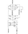
次に、前記各ドライバ回路およびディストリビュータ回路の構成について説明する。
〈WLドライバ回路〉
プログラムパルス印加時、選択WLは10V、非選択WLはGNDに設定する(図12のプログラム動作時のt7参照)。
Next, the configuration of each driver circuit and distributor circuit will be described.
<WL driver circuit>
When the program pulse is applied, the selected WL is set to 10 V, and the non-selected WL is set to GND (see t7 during the program operation in FIG. 12).
消去パルス印加時、選択WLは−6V、非選択WLはVCC(=1.8V)に設定する(図14の消去動作時のt2参照)。 When the erase pulse is applied, the selection WL is set to -6V, and the non-selection WL is set to VCC (= 1.8V) (see t2 during the erase operation in FIG. 14).
選択WLに正及び負の電圧を供給するデコーダ回路には、例えば特許第3223877号に開示された構成がある。 An example of a decoder circuit that supplies positive and negative voltages to the selection WL is disclosed in Japanese Patent No. 3223877.
しかし、この構成では、非選択WLが0Vに固定されており、今回のWLデコーダ動作に適合しない。そこで、図16に示した構成により、非選択WLをVCC及びGNDに変更できる回路を実現した。 However, in this configuration, the non-selected WL is fixed at 0V, which is not suitable for the current WL decoder operation. Therefore, a circuit capable of changing the non-selected WL to VCC and GND is realized by the configuration shown in FIG.
図16はWLドライバ回路である。この図16において、VPWLはVCC以上の正の高電圧であり、後述するディストリビュータ回路を介して正チャージポンプ回路から電圧を受ける。 FIG. 16 shows a WL driver circuit. In FIG. 16, VPWL is a positive high voltage equal to or higher than VCC, and receives a voltage from the positive charge pump circuit via a distributor circuit described later.
一方、VNWLはGND以下の負の高電圧であり、後述するディストリビュータ回路を介して負チャージポンプ回路から電圧を受ける。トランジスタN6、N7、P6、P7、及びインバータ15から成るレベルシフト回路17は、入力信号SELWLの[VCC,GND]の2値信号を[VPWL,GND]に変換する。
On the other hand, VNWL is a negative high voltage equal to or lower than GND, and receives a voltage from a negative charge pump circuit via a distributor circuit described later. A
レベルシフト回路17から信号を受けたレベルシフト回路18はトランジスタN5、N4、P5、P4から成り、入力信号[VPWL,GND]の2値信号を[VPWL,VNWL]に変換し、ノードVSELWLに供給する。
The
一方、トランジスタN12,N13,P12,P13、及びインバータ16から成るレベルシフト回路19は、WL選択アドレス信号をデコードするANDゲート17の出力[VCC,GND]の2値信号を受け[VPWL,GND]に変換する。
On the other hand, a
レベルシフト回路19から信号を受けたレベルシフト回路20は、トランジスタN10,N11,P10,P11から成り、入力信号[VPWL,GND]の2値信号を[VPWL,VNWL]に変換し、トランジスタN9,P9からなるインバータに供給する。
The
トランジスタN9,P9からなるインバータの出力はDECWL1とする。 The output of the inverter composed of the transistors N9 and P9 is DECWL1.
DECWL1はトランジスタN8,P8からなるインバータに入力され、当該インバータはDECWL0を出力する。 DECWL1 is input to an inverter composed of transistors N8 and P8, and the inverter outputs DECWL0.
アドレスが選択状態になり、ANDゲート17の出力がVCCのとき、DECWL1がVPWLに、DECWL0がVNWLになる。このとき、トランジスタN2,P1がONし、トランジスタN1,P2がOFFするので、WLにはVSELWLの電圧が伝播する。これがWL選択状態である。
When the address is selected and the output of the AND
前述のとおり、SELWL=VCCのとき、VSELWL=VPWLとなり、選択状態のWLに正の高電圧が印加される。
また、SELWL=GNDのとき、VSELWL=VNWLとなり、選択状態のWLに負の高電圧が印加される。
これにより選択WLには正負の高電圧を印加することができる。
As described above, when SELWL = VCC, VSELWL = VPWL, and a positive high voltage is applied to the selected WL.
Further, when SELWL = GND, VSELWL = VNWL, and a negative high voltage is applied to the selected WL.
Thereby, a positive and negative high voltage can be applied to the selection WL.
一方、アドレスが非選択状態になり、ANDゲート17の出力がGNDのとき、DECWL1がVNWLに、DECWL0がVPWLになる。
On the other hand, when the address is in a non-selected state and the output of the AND
このとき、トランジスタN2,P1がOFFし、トランジスタN1,P2がONするのでWLにはVUSELWLの電圧が伝播する。これがWL非選択状態である。 At this time, since the transistors N2 and P1 are turned off and the transistors N1 and P2 are turned on, the voltage VUSELWL propagates to WL. This is the WL non-selected state.
USELWLがGNDのときVUSELWLはインバータ14によりVCCになり、非選択WLはVCCとなる。
When USELWL is GND, VUSELWL is set to VCC by the
また、USELWLがVCCのときVUSELWLはインバータ14によりGNDになり、非選択WLはGNDとなる。
When USELWL is VCC, VUSEWL is set to GND by the
以上のような構成によれば、選択WLを正負の高電圧に設定でき、かつ非選択のWLをVCC/GNDに設定できる。 According to the above configuration, the selected WL can be set to a positive and negative high voltage, and the non-selected WL can be set to VCC / GND.
〈SGドライバ回路〉
図17はSGドライバ回路の構成を示す図である。素子の記号はWLドライバ回路の各素子と対応する。SGドライバ回路の構成はWLドライバ回路と同様であるが、WLドライバ回路においてVUSELWL信号に相当する部分がVCCになっている。これはSGにおいては非選択SGのレベルが各動作条件で常にVCCになっているためである。
<SG driver circuit>
FIG. 17 is a diagram showing the configuration of the SG driver circuit. The symbol of the element corresponds to each element of the WL driver circuit. The configuration of the SG driver circuit is the same as that of the WL driver circuit, but the portion corresponding to the VUSELWL signal in the WL driver circuit is VCC. This is because in SG, the level of the non-selected SG is always VCC in each operating condition.
このような構成によれば、選択SGを正負の高電圧VPSGに設定でき、非選択WLをVCCにできる。 According to such a configuration, the selection SG can be set to a positive and negative high voltage VPSG, and the non-selection WL can be set to VCC.
〈WELドライバ回路〉
図18はWELドライバ回路の構成を示す図である。
この構成によれば、選択WELにはVPWELレベルが、非選択WELにはVCCがそれぞれ供給される。
<WEL driver circuit>
FIG. 18 is a diagram showing the configuration of the WEL driver circuit.
According to this configuration, the VPWEL level is supplied to the selected WEL, and VCC is supplied to the non-selected WEL.
〈WELSGドライバ回路〉
図19はWELSGドライバ回路の構成を示す図である。
この構成によれば、選択WELSGにはVPWELSGレベルが、非選択WELSGにはVCCがそれぞれ供給される。
<WELSG driver circuit>
FIG. 19 is a diagram showing the configuration of the WELSG driver circuit.
According to this configuration, the VPWELSG level is supplied to the selected WELSG, and VCC is supplied to the non-selected WELSG.
〈SLドライバ回路〉
図20は、SLドライバ回路の構成を示す図である。
SLにはVCC、GND及び消去時の6Vが印加される。高電圧の6VはVPSLへ供給される。デコード信号により選択状態になると、トランジスタP1、N2がON状態、トランジスタN1がOFF状態になり、SLへはVSELSLが伝播される。
<SL driver circuit>
FIG. 20 is a diagram illustrating a configuration of the SL driver circuit.
VCC, GND and 6V at the time of erasing are applied to SL. A high voltage of 6V is supplied to VPSL. When selected by the decode signal, the transistors P1 and N2 are turned on, the transistor N1 is turned off, and VSELSL is propagated to SL.
一方、非選択状態になると、トランジスタP1,N2がOFF状態、トランジスタN1がON状態になり、SLへはGNDが伝播される。 On the other hand, in the non-selected state, the transistors P1 and N2 are turned off, the transistor N1 is turned on, and GND is propagated to SL.
消去ベリファイ時(t9)及びプログラムベリファイ時(t16)においては、選択SLをGNDに変化させ、当該SLに接続されているプログラム状態のメモリセル群を通じてSBL及びMBLを放電する。 At the time of erase verify (t9) and program verify (t16), the selected SL is changed to GND, and SBL and MBL are discharged through the memory cell group in the programmed state connected to the SL.
選択SLをGNDに変化させるには、/SETHをHにすることにより実現する。 The selection SL is changed to GND by setting / SETH to H.
〈ディストリビュータ回路〉
WLドライバ回路は図16に示すように、VCC以上の正の高電圧としてVPWLを、また、GND以下の負の高電圧としてVNWLをそれぞれディストリビュータ回路から受けている。
<Distributor circuit>
As shown in FIG. 16, the WL driver circuit receives VPWL as a positive high voltage equal to or higher than VCC and VNWL as a negative high voltage equal to or lower than GND from the distributor circuit.
以下に、このディストリビュータ回路に関して説明する。
図21はディストリビュータ回路の構成を示す図である。VPHは第1の正チャージポンプ回路、VPLは第2の正チャージポンプ回路であり、VNHは第1の負チャージポンプ回路、VNLは第2の負チャージポンプである。
Hereinafter, the distributor circuit will be described.
FIG. 21 is a diagram showing the configuration of the distributor circuit. VPH is a first positive charge pump circuit, VPL is a second positive charge pump circuit, VNH is a first negative charge pump circuit, and VNL is a second negative charge pump circuit.
チャージポンプ回路とは例えば特許第2141320号に開示される高電圧発生回路であり、その活性信号(図示せず)を受けて出力端子に高電圧を与えるものである。 The charge pump circuit is a high voltage generating circuit disclosed in, for example, Japanese Patent No. 2141320, and receives an activation signal (not shown) and applies a high voltage to an output terminal.
また、特許第2141320号に開示されるチャージポンプは、その出力電圧のレベルを感知してこれをフードバックすることにより、所望の電圧レベルを発生させることができる。
チャージポンプVPHの出力は正切り替え回路SP1を通じてVPWLに接続されている。
The charge pump disclosed in Japanese Patent No. 2141320 can generate a desired voltage level by sensing the level of the output voltage and hooding it back.
The output of the charge pump VPH is connected to VPWL through the positive switching circuit SP1.
正切り替え回路SP1は、制御信号(図示せず)に応じてVPHの出力とVPWLとを電気的に接続するモードと電源VCCとVPWLとを電気的に接続するモードとを持つ。具体的には、例えば特許第2658916号に開示された回路と同様の、図22に示す回路で実現できる。 Positive switching circuit SP1 has a mode for electrically connecting the output of VPH and VPWL and a mode for electrically connecting power supplies VCC and VPWL in accordance with a control signal (not shown). Specifically, for example, the circuit shown in FIG. 22 similar to the circuit disclosed in Japanese Patent No. 2658916 can be realized.
ここで、VPHの出力とVPWLとを電気的に接続するときは、SELVPHをHにする。このとき、トランジスタN13,N14,P13,P14から成るレベルシフト回路により、トランジスタP16はON状態になり、かつ、トランジスタN11,N12,P11,P12から成るレベルシフト回路により、トランジスタP15はON状態になる。 Here, when the output of VPH and VPWL are electrically connected, SELVPH is set to H. At this time, the transistor P16 is turned on by the level shift circuit composed of the transistors N13, N14, P13, and P14, and the transistor P15 is turned on by the level shift circuit composed of the transistors N11, N12, P11, and P12. .
一方、トランジスタN16はOFF状態である。これにより、VPHとVPWLとが電気的に接続される。 On the other hand, the transistor N16 is in an OFF state. Thereby, VPH and VPWL are electrically connected.
VCCとVPWLとを電気的に接続するときは、SELVCCをHにする。このとき、トランジスタN3,N4,P3,P4から成るレベルシフト回路により、トランジスタP6はON状態になり、かつ、トランジスタN1,N2,P1,P2から成るレベルシフト回路により、トランジスタP5はON状態になる。 When electrically connecting VCC and VPWL, SELVCC is set to H. At this time, the transistor P6 is turned on by the level shift circuit composed of the transistors N3, N4, P3, and P4, and the transistor P5 is turned on by the level shift circuit composed of the transistors N1, N2, P1, and P2. .
一方、トランジスタN6はOFF状態である。これにより、VCCとVPWLとが電気的に接続される。
チャージポンプVNHの出力は負切り替え回路SN1を通じてVNWLに接続されている。
On the other hand, the transistor N6 is in an OFF state. Thereby, VCC and VPWL are electrically connected.
The output of the charge pump VNH is connected to VNWL through the negative switching circuit SN1.
負切り替え回路SN1は制御信号(図示せず)に応じて、VNHの出力とVNWLとを電気的に接続するモードと電源GNDとVNWLとを電気的に接続するモードとを持つ。 The negative switching circuit SN1 has a mode for electrically connecting the output of VNH and VNWL and a mode for electrically connecting power supplies GND and VNWL in accordance with a control signal (not shown).
具体的な回路は、例えば特許第2658916号に開示された回路と同様の、図23の構成で実現できる。 A specific circuit can be realized by the configuration of FIG. 23 similar to the circuit disclosed in, for example, Japanese Patent No. 2658916.
VNHの出力とVNWLとを電気的に接続するときは、SELVNHをLにする。 When electrically connecting the output of VNH and VNWL, SELVNH is set to L.
このとき、トランジスタN13、N14、P13、P14から成るレベルシフト回路により、トランジスタN16はON状態になり、かつ、トランジスタN11、N12、P11、P12から成るレベルシフト回路により、トランジスタN15はON状態になる。 At this time, the transistor N16 is turned on by the level shift circuit composed of the transistors N13, N14, P13, and P14, and the transistor N15 is turned on by the level shift circuit composed of the transistors N11, N12, P11, and P12. .
一方トランジスタP16はOFF状態である。
これにより、VNHとVNWLとが電気的に接続される。
On the other hand, the transistor P16 is in an OFF state.
Thereby, VNH and VNWL are electrically connected.
GNDとVNWLとを電気的に接続するときは、SELGNDをLにする。このとき、トランジスタN3,N4,P3,P4から成るレベルシフト回路により、トランジスタN6はON状態になり、かつ、トランジスタN1,N2,P1,P2から成るレベルシフト回路により、トランジスタN5はON状態になる。一方トランジスタP6はOFF状態である。
これにより、GNDとVNWLとが電気的に接続される。
To electrically connect GND and VNWL, SELGND is set to L. At this time, the transistor N6 is turned on by the level shift circuit composed of the transistors N3, N4, P3, and P4, and the transistor N5 is turned on by the level shift circuit composed of the transistors N1, N2, P1, and P2. . On the other hand, the transistor P6 is in an OFF state.
Thereby, GND and VNWL are electrically connected.
以上のような構成により、VPWLへはVPHかVCCかいずれかの電圧が、VNWLへはVNHかGNDかいずれかの電圧がそれぞれ伝播される。 With the above configuration, either VPH or VCC is transmitted to VPWL, and either VNH or GND is transmitted to VNWL.
SGドライバ回路は図17に示すように、VCC以上の正の高電圧としてVPSGを、また、GND以下の負の高電圧としてVNSGをそれぞれ高電圧切り替え回路から受けている。 As shown in FIG. 17, the SG driver circuit receives VPSG as a positive high voltage equal to or higher than VCC and VNSG as a negative high voltage equal to or lower than GND from the high voltage switching circuit.
図21において、チャージポンプVPHの出力は正切り替え回路SP2を通じてVPSGに接続されている。チャージポンプVNLの出力は負切り替え回路SN2を通じてVNSGに接続されている。 In FIG. 21, the output of the charge pump VPH is connected to VPSG through the positive switching circuit SP2. The output of the charge pump VNL is connected to VNSG through the negative switching circuit SN2.
このような構成により、VPSGへはVPHかVCCのいずれかの電圧が、VNSGへはVNLかGNDのいずれかの電圧がそれぞれ伝播される。 With such a configuration, either VPH or VCC voltage is propagated to VPSG, and either VNL or GND voltage is propagated to VNSG.
また、チャージポンプVPLの出力は、正切り替え回路SP3,SP4,SP5を介してVPSL,VPWEL,VPWELSGにそれぞれ接続されている。 The output of the charge pump VPL is connected to VPSL, VPWEL, and VPWELSG via positive switching circuits SP3, SP4 and SP5, respectively.
以上説明したように、この実施形態では、バックゲート電圧を印加してソースにドレイン電圧とソース電圧の中間の電圧を印加したことにより、ドレイン−ソース間に掛かる電圧が下がることと、バックゲート効果により等価的にVth(絶対値)が高くなるためにパンチスルーしにくくなり、これによって、ゲート長のスケーラビリティ(短ゲート化)を大幅に改善することが可能になり、NOR型の構造において、0.1μm以下のゲート長を実現することも困難でなくなった。 As described above, in this embodiment, by applying a back gate voltage and applying a voltage between the drain voltage and the source voltage to the source, the voltage applied between the drain and the source decreases, and the back gate effect Therefore, Vth (absolute value) is equivalently increased, so that punch-through is difficult, which makes it possible to greatly improve the scalability of the gate length (short gate). It is no longer difficult to realize a gate length of 1 μm or less.
また、この実施形態では、消去ベリファイ時に、選択ブロック内の全てにワード線に同一のベリファイ電圧を与えることによってブロック内の全てのメモリセルを一回の読み出しでベリファイでき、消去ベリファイの時間を短縮できる。 Further, in this embodiment, at the time of erase verify, all the memory cells in the block can be verified by a single read operation by applying the same verify voltage to the word lines in all of the selected blocks, thereby shortening the time of erase verify. it can.
なお、本実施形態では、pチャネルMONOS構造のメモリセルに対する書込方法について説明しているが、図3の電位配置等の極性を反転することにより、この発明をnチャネルMONOSメモリに適用することも可能である。 In this embodiment, a writing method for a memory cell having a p-channel MONOS structure has been described. However, the present invention is applied to an n-channel MONOS memory by inverting the polarity of the potential arrangement in FIG. Is also possible.
また、本実施形態では、図1に示したMONOS構造のメモリセルに対する書込方法を説明しているが、これ以外にも、フローティングゲート型の不揮発性半導体メモリ、ナノクリスタル層に電荷を保持する不揮発性半導体メモリ等に適用することができる。 In this embodiment, the writing method for the memory cell having the MONOS structure shown in FIG. 1 is described. However, in addition to this, the floating gate type nonvolatile semiconductor memory holds charges in the nanocrystal layer. The present invention can be applied to a nonvolatile semiconductor memory or the like.
なお、図3等に示した電圧値は一例であり、本発明の条件に合致する電圧であればどのような電圧でもよい。 Note that the voltage values shown in FIG. 3 and the like are merely examples, and any voltage may be used as long as the voltage meets the conditions of the present invention.
11…p型半導体基板
12…n型ウェル(セルウェル)
13…ソース(p+領域)
14…ドレイン(p+領域)
15…トンネル絶縁膜
16…電荷トラップ層(窒化膜)
17…上部絶縁層
18…ゲート
20…セレクトゲートウェル(n型ウェル)
21…メインビット線
22…ワード線
23…ソース線
24…セレクトゲート
25…サブビット線
11 ... p-
13 ... Source (p + region)
14 ... Drain (p + region)
15 ...
17 ... Upper insulating
21 ...
Claims (1)
前記ソース−ドレイン間に形成されたチャンネル領域と、前記チャンネル領域の上方にトンネル絶縁膜を介して形成された電荷蓄積層と、前記電荷蓄積層の上方に絶縁膜を介して形成されたゲート電極と、を有する不揮発性半導体記憶装置のメモリセルの読み書き方法であって、
書き込み時に、電源電圧をVCCで表し、
「VP>VSB>Vs>Vd」「VSB>0V」「Vd≦VCC」
の関係を有する電圧VP、VSB、VsおよびVdを、それぞれゲート電極、前記n型ウェル電極、ソース電極およびドレイン電極に印加することにより、ドレイン付近にバンド間トンネリングによるホットエレクトロンを発生させ、このホットエレクトロンを前記電荷蓄積層に注入して前記メモリセルにビットデータの書き込みを行い、
消去に続く消去ベリファイ時に、選択ブロック内の全てのワード線に同一のベリファイ電圧を与えることを特徴とする不揮発性半導体記憶装置の読み書き制御方法。 An n-type well formed in a semiconductor substrate, a source and a drain formed in the n-type well,
A channel region formed between the source and drain; a charge storage layer formed above the channel region via a tunnel insulating film; and a gate electrode formed above the charge storage layer via an insulating film A method for reading and writing memory cells of a nonvolatile semiconductor memory device, comprising:
When writing, the power supply voltage is represented by VCC,
“VP>VSB>Vs> Vd” “VSB> 0 V” “Vd ≦ VCC”
Are applied to the gate electrode, the n-type well electrode, the source electrode, and the drain electrode, respectively, thereby generating hot electrons due to band-to-band tunneling near the drain. Injecting electrons into the charge storage layer to write bit data to the memory cell,
A read / write control method for a nonvolatile semiconductor memory device, wherein the same verify voltage is applied to all word lines in a selected block at the time of erase verify following erase.
Priority Applications (1)
| Application Number | Priority Date | Filing Date | Title |
|---|---|---|---|
| JP2005265080A JP4832835B2 (en) | 2005-09-13 | 2005-09-13 | Read / write control method for nonvolatile semiconductor memory device |
Applications Claiming Priority (1)
| Application Number | Priority Date | Filing Date | Title |
|---|---|---|---|
| JP2005265080A JP4832835B2 (en) | 2005-09-13 | 2005-09-13 | Read / write control method for nonvolatile semiconductor memory device |
Related Child Applications (1)
| Application Number | Title | Priority Date | Filing Date |
|---|---|---|---|
| JP2011167479A Division JP5238859B2 (en) | 2011-07-29 | 2011-07-29 | Nonvolatile semiconductor memory device and read / write control method thereof |
Publications (3)
| Publication Number | Publication Date |
|---|---|
| JP2007080338A JP2007080338A (en) | 2007-03-29 |
| JP2007080338A5 JP2007080338A5 (en) | 2008-10-23 |
| JP4832835B2 true JP4832835B2 (en) | 2011-12-07 |
Family
ID=37940501
Family Applications (1)
| Application Number | Title | Priority Date | Filing Date |
|---|---|---|---|
| JP2005265080A Expired - Fee Related JP4832835B2 (en) | 2005-09-13 | 2005-09-13 | Read / write control method for nonvolatile semiconductor memory device |
Country Status (1)
| Country | Link |
|---|---|
| JP (1) | JP4832835B2 (en) |
Families Citing this family (4)
| Publication number | Priority date | Publication date | Assignee | Title |
|---|---|---|---|---|
| JP5343916B2 (en) | 2010-04-16 | 2013-11-13 | 富士通セミコンダクター株式会社 | Semiconductor memory |
| JP2013218758A (en) * | 2012-04-06 | 2013-10-24 | Genusion:Kk | Nonvolatile semiconductor memory device |
| US10269822B2 (en) | 2015-12-29 | 2019-04-23 | Taiwan Semiconductor Manufacturing Co., Ltd. | Method to fabricate uniform tunneling dielectric of embedded flash memory cell |
| CN107039452B (en) * | 2015-12-29 | 2020-02-21 | 台湾积体电路制造股份有限公司 | Method of fabricating uniform tunnel dielectric for embedded flash memory cells |
Family Cites Families (5)
| Publication number | Priority date | Publication date | Assignee | Title |
|---|---|---|---|---|
| JP3878681B2 (en) * | 1995-06-15 | 2007-02-07 | 株式会社ルネサステクノロジ | Nonvolatile semiconductor memory device |
| JP2888181B2 (en) * | 1995-09-18 | 1999-05-10 | 日本電気株式会社 | Nonvolatile semiconductor memory device |
| US5687118A (en) * | 1995-11-14 | 1997-11-11 | Programmable Microelectronics Corporation | PMOS memory cell with hot electron injection programming and tunnelling erasing |
| JPH09246404A (en) * | 1996-03-04 | 1997-09-19 | Mitsubishi Electric Corp | Non-volatile semiconductor memory |
| JP3962769B2 (en) * | 2004-11-01 | 2007-08-22 | 株式会社Genusion | Nonvolatile semiconductor memory device and writing method thereof |
-
2005
- 2005-09-13 JP JP2005265080A patent/JP4832835B2/en not_active Expired - Fee Related
Also Published As
| Publication number | Publication date |
|---|---|
| JP2007080338A (en) | 2007-03-29 |
Similar Documents
| Publication | Publication Date | Title |
|---|---|---|
| KR100458412B1 (en) | Level shifter for transforming voltage level and semiconductor memory device having the level shifter | |
| US6288944B1 (en) | NAND type nonvolatile memory with improved erase-verify operations | |
| US9984761B2 (en) | Semiconductor memory device | |
| JP4084922B2 (en) | Non-volatile memory device writing method | |
| JP3886673B2 (en) | Nonvolatile semiconductor memory device | |
| US8017994B2 (en) | Nonvolatile semiconductor memory | |
| JP4562602B2 (en) | Memory cell and related operation method | |
| JP4434405B2 (en) | Nonvolatile semiconductor memory device | |
| KR100706247B1 (en) | Flash memory device and read method thereof | |
| JP3694422B2 (en) | Row decoder circuit | |
| JP3976774B1 (en) | Nonvolatile semiconductor memory device and control method thereof | |
| JP2000236031A (en) | Nonvolatile semiconductor memory | |
| JP4832835B2 (en) | Read / write control method for nonvolatile semiconductor memory device | |
| WO2006059375A1 (en) | Semiconductor device and semiconductor device control method | |
| US6567314B1 (en) | Data programming implementation for high efficiency CHE injection | |
| JPH11134879A (en) | Nonvolatile semiconductor storage device | |
| JP4113559B2 (en) | Nonvolatile semiconductor memory device and writing method thereof | |
| JP2007080338A5 (en) | ||
| KR100784863B1 (en) | Flash memory device with improved program performance and program mehtod thereof | |
| US5923589A (en) | Non-volatile semiconductor memory device having long-life memory cells and data erasing method | |
| JP5238859B2 (en) | Nonvolatile semiconductor memory device and read / write control method thereof | |
| JP2004503898A (en) | Method for reducing the capacitive load of a flash memory x-decoder to accurately control the voltage on word and select lines | |
| JP3263636B2 (en) | Nonvolatile semiconductor memory device | |
| WO2007043136A9 (en) | Nand-type flash memory preventing disturbance | |
| TW520493B (en) | Flash memory cell and method to achieve multiple bits per cell |
Legal Events
| Date | Code | Title | Description |
|---|---|---|---|
| A521 | Request for written amendment filed |
Free format text: JAPANESE INTERMEDIATE CODE: A523 Effective date: 20080827 |
|
| A621 | Written request for application examination |
Free format text: JAPANESE INTERMEDIATE CODE: A621 Effective date: 20080827 |
|
| RD04 | Notification of resignation of power of attorney |
Free format text: JAPANESE INTERMEDIATE CODE: A7424 Effective date: 20100830 |
|
| RD03 | Notification of appointment of power of attorney |
Free format text: JAPANESE INTERMEDIATE CODE: A7423 Effective date: 20100916 |
|
| A131 | Notification of reasons for refusal |
Free format text: JAPANESE INTERMEDIATE CODE: A131 Effective date: 20110531 |
|
| A521 | Request for written amendment filed |
Free format text: JAPANESE INTERMEDIATE CODE: A523 Effective date: 20110729 |
|
| TRDD | Decision of grant or rejection written | ||
| A01 | Written decision to grant a patent or to grant a registration (utility model) |
Free format text: JAPANESE INTERMEDIATE CODE: A01 Effective date: 20110823 |
|
| A01 | Written decision to grant a patent or to grant a registration (utility model) |
Free format text: JAPANESE INTERMEDIATE CODE: A01 |
|
| A61 | First payment of annual fees (during grant procedure) |
Free format text: JAPANESE INTERMEDIATE CODE: A61 Effective date: 20110921 |
|
| R150 | Certificate of patent or registration of utility model |
Free format text: JAPANESE INTERMEDIATE CODE: R150 |
|
| FPAY | Renewal fee payment (event date is renewal date of database) |
Free format text: PAYMENT UNTIL: 20140930 Year of fee payment: 3 |
|
| R250 | Receipt of annual fees |
Free format text: JAPANESE INTERMEDIATE CODE: R250 |
|
| R250 | Receipt of annual fees |
Free format text: JAPANESE INTERMEDIATE CODE: R250 |
|
| R255 | Notification that request for automated payment was rejected |
Free format text: JAPANESE INTERMEDIATE CODE: R2525 |
|
| R250 | Receipt of annual fees |
Free format text: JAPANESE INTERMEDIATE CODE: R250 |
|
| R250 | Receipt of annual fees |
Free format text: JAPANESE INTERMEDIATE CODE: R250 |
|
| LAPS | Cancellation because of no payment of annual fees |