JP4829598B2 - Multi-bit storage device and multi-bit storage method - Google Patents
Multi-bit storage device and multi-bit storage method Download PDFInfo
- Publication number
- JP4829598B2 JP4829598B2 JP2005335528A JP2005335528A JP4829598B2 JP 4829598 B2 JP4829598 B2 JP 4829598B2 JP 2005335528 A JP2005335528 A JP 2005335528A JP 2005335528 A JP2005335528 A JP 2005335528A JP 4829598 B2 JP4829598 B2 JP 4829598B2
- Authority
- JP
- Japan
- Prior art keywords
- memory
- data
- initialization
- address
- storage device
- Prior art date
- Legal status (The legal status is an assumption and is not a legal conclusion. Google has not performed a legal analysis and makes no representation as to the accuracy of the status listed.)
- Active
Links
Images


Classifications
-
- Y—GENERAL TAGGING OF NEW TECHNOLOGICAL DEVELOPMENTS; GENERAL TAGGING OF CROSS-SECTIONAL TECHNOLOGIES SPANNING OVER SEVERAL SECTIONS OF THE IPC; TECHNICAL SUBJECTS COVERED BY FORMER USPC CROSS-REFERENCE ART COLLECTIONS [XRACs] AND DIGESTS
- Y02—TECHNOLOGIES OR APPLICATIONS FOR MITIGATION OR ADAPTATION AGAINST CLIMATE CHANGE
- Y02D—CLIMATE CHANGE MITIGATION TECHNOLOGIES IN INFORMATION AND COMMUNICATION TECHNOLOGIES [ICT], I.E. INFORMATION AND COMMUNICATION TECHNOLOGIES AIMING AT THE REDUCTION OF THEIR OWN ENERGY USE
- Y02D10/00—Energy efficient computing, e.g. low power processors, power management or thermal management
Landscapes
- Memory System (AREA)
Description
本発明は、複数のビットから構成されるデータを記憶する多ビット記憶装置及びそれを用いた多ビット記憶方法に関する。 The present invention relates to a multi-bit storage device that stores data composed of a plurality of bits and a multi-bit storage method using the same.
従来より、複数のビットから構成されるデータを記憶する装置として、フリップフロップ(以下、F/Fと称する)を用いたレジスタが記憶素子として使用される記憶装置やメモリが記憶素子として使用される記憶装置等が挙げられる。 Conventionally, as a device for storing data composed of a plurality of bits, a storage device using a register using a flip-flop (hereinafter referred to as F / F) or a memory is used as a storage device. Examples thereof include a storage device.
F/Fが記憶素子として使用される記憶装置の場合、F/Fの動作による消費電力が大きくなってしまうため、その消費電力の低減が課題とされる。 In the case of a storage device in which the F / F is used as a storage element, power consumption due to the operation of the F / F increases, and thus reduction of the power consumption is an issue.
図5は、従来のF/Fが記憶素子として使用された多ビット記憶装置の一構成例を示す図である。 FIG. 5 is a diagram illustrating a configuration example of a multi-bit storage device in which a conventional F / F is used as a storage element.
図5に示した多ビット記憶装置は、チップセレクト生成部501と、ライトパルス生成部502と、レジスタ部503と、リードデータ選択部504とから構成されている。チップセレクト生成部501は、ライトデータが記憶されるレジスタ部503のアドレスと、ライトデータがライトされるタイミングを示す信号であるライトイネーブルとが入力され、それらに基づいて各アドレスに応じたチップセレクト1〜nを生成する。ライトパルス生成部502は、クロックと、チップセレクト生成部501にて生成されたチップセレクト1〜nとが入力され、クロックにチップセレクト1〜nでゲートをかけることにより、チップセレクト1〜nが有効な区間のみクロックをライトパルス1〜nとして出力する。レジスタ部503には、複数のF/F531−1〜531−nが設けられており、それぞれが1つのアドレスと対応しており、該当するアドレスによって指定されたエリアにライトデータを記憶する。F/F531−1〜531−nの動作は、一般的なF/Fの動作と同様であり、「D」端子に入力されたデータを「CLK」端子に入力されたクロックで打ち抜くことにより、データを記憶する。リードデータ選択部504は、アドレスと、レジスタ部503のF/F531−1〜531−nから出力されたリードデータ1〜nとが入力され、アドレスに基づいてそれらのリードデータ1〜nの中から1つのリードデータを選択する。
The multi-bit storage device shown in FIG. 5 includes a chip
上述した構成において、レジスタへ供給されるクロックに不要な時にはゲートをかけることにより、F/F531−1〜531−nの消費電力の低減を図っている。 In the configuration described above, the power consumption of the F / Fs 531-1 to 531-n is reduced by applying a gate to the clock supplied to the register when unnecessary.
一方、メモリが記憶素子として使用される記憶装置の場合、F/Fよりもメモリの方が消費電力が少ないが、装置の初期化時にメモリの全エリアの初期化をしなければならない。容易に初期化できる機能を有するメモリであれば良いが、そのような初期化機能を有しないメモリの場合は、初期化を行う煩雑な処理が必要となってしまう。 On the other hand, in the case of a storage device in which the memory is used as a storage element, the memory consumes less power than the F / F, but all areas of the memory must be initialized when the device is initialized. A memory having a function that can be easily initialized may be used. However, in the case of a memory that does not have such an initialization function, a complicated process for performing initialization is required.
そこで、メモリのアドレスをビットマップで表し、所定のビットがラッチ回路に予め格納された値と同一であるアドレスにエントリーされているデータのみを一括で初期化(クリア)する方法が考えられている(例えば、特許文献1参照。)。 In view of this, a method has been considered in which the memory address is represented by a bit map, and only data entered at an address where a predetermined bit is the same as the value stored in advance in the latch circuit is initialized (cleared). (For example, refer to Patent Document 1).
また、メモリ自体を初期化するのではなく、ライトアクセスされたメモリのアドレスを記憶しておき、メモリがリードアクセスされた際に記憶されたアドレスとリードアクセスされたアドレスとを比較し、比較した結果、記憶されたアドレスとリードアクセスされたアドレスとが一致しない場合、リードアクセスされたメモリのアドレスに記憶されているデータではなく、予めレジスタ等に記憶されている初期値データを出力することにより、電源投入直後等の初期状態にメモリ内に残っている不定データをリードしてしまうことを避ける方法が考えられている(例えば、特許文献2参照。)。
しかしながら、図5に示した従来のF/Fが記憶素子として使用された多ビット記憶装置では、F/Fの数がライトデータのバス幅分×必要アドレス分必要となり、F/Fの消費電力の低減ができないという問題点がある。また、F/Fに入力されるクロックにゲートをかけているため、ゲートをかけられたクロックとゲートをかけられたクロックによって打ち抜かれる信号との位相関係が不安定となり、誤動作の原因になってしまうという問題点がある。 However, in the multi-bit storage device in which the conventional F / F shown in FIG. 5 is used as a storage element, the number of F / Fs is required for the write data bus width × required address, and the F / F power consumption There is a problem that it cannot be reduced. In addition, since the clock input to the F / F is gated, the phase relationship between the gated clock and the signal punched out by the gated clock becomes unstable, causing malfunction. There is a problem that.
また、特許文献1に記載された方法においては、初期化するアドレスを指定するためのラッチ回路を構成するには、少なくともアドレスのビット数と同数のF/Fが必要となり、装置としての消費電力の低減ができないという問題点がある。
Further, in the method described in
また、特許文献2に記載された方法においては、メモリがライトアクセスされる度に、そのライトアクセスされたアドレスを記憶しなければならなく、さらに記憶するためのメモリ等の記憶手段を設けなければならないという問題点がある。
Further, in the method described in
本発明は、上述したような従来の技術が有する問題点に鑑みてなされたものであって、装置の消費電力を容易に低減できる多ビット記憶装置及び多ビット記憶方法を提供することを目的とする。 The present invention has been made in view of the problems of the conventional techniques as described above, and an object thereof is to provide a multi-bit storage device and a multi-bit storage method capable of easily reducing the power consumption of the device. To do.
上記目的を達成するために本発明は、
複数のビットから構成されるデータを記憶する多ビット記憶装置であって、
前記多ビット記憶装置のリセット後、メモリ内の、外部から入力されたアドレスによって指定されたエリアへの外部から入力されたデータの書き込み処理が終了するまでは無効となり、該データの書き込み処理が終了した後は有効となる初期化解除信号を生成し、前記初期化解除信号が無効である場合、予め設定された初期値を選択して出力し、また、前記初期化解除信号が有効である場合は、前記メモリから読み出されたデータを選択して出力する。
In order to achieve the above object, the present invention provides:
A multi-bit storage device for storing data composed of a plurality of bits,
After resetting the multi-bit storage device, it becomes invalid until the processing of writing data input from the outside to the area specified by the address input from the outside in the memory is completed, and the processing of writing the data ends. When the initialization cancellation signal that becomes valid is generated and the initialization cancellation signal is invalid, a preset initial value is selected and output, and the initialization cancellation signal is valid Selects and outputs data read from the memory.
また、前記データを記憶するメモリと、
前記多ビット記憶装置のリセット後、前記メモリ内の、外部から入力されたアドレスによって指定されたエリアへの外部から入力されたデータの書き込み処理が終了するまでは無効となり、該データの書き込み処理が終了した後は有効となる初期化解除信号を生成する初期化監視手段と、
前記初期化解除信号が無効である場合、予め設定された初期値を選択して出力し、また、前記初期化解除信号が有効である場合は、前記メモリから読み出されたデータを選択して出力するデータ選択手段とを有することを特徴とする。
A memory for storing the data;
After resetting of the multi-bit memory device, in said memory, until the writing process of data input from the outside to the specified area by the address inputted from the outside is finished becomes invalid, writing process of the data Initialization monitoring means for generating an initialization cancellation signal that becomes valid after the completion,
When the initialization release signal is invalid, a preset initial value is selected and output, and when the initialization release signal is valid, the data read from the memory is selected. And a data selection means for outputting.
また、前記初期化監視手段は、1つの前記アドレスにつき1つのフリップフロップによって初期化解除信号を生成することを特徴とする。 Further, the initialization monitoring means generates an initialization cancellation signal by one flip-flop for each address.
また、複数のビットから構成されるデータを記憶する多ビット記憶装置における多ビット記憶方法であって、
前記多ビット記憶装置のリセット後、メモリ内の、外部から入力されたアドレスによって指定されたエリアへの外部から入力されたデータの書き込み処理が終了するまでは無効となり、該データの書き込み処理が終了した後は有効となる初期化解除信号を生成する処理と、
前記初期化解除信号が無効である場合、予め設定された初期値を選択して出力する処理と、
前記初期化解除信号が有効である場合は、前記メモリから読み出されたデータを選択して出力する処理とを有する。
Further, a multi-bit storage method in a multi-bit storage device for storing data composed of a plurality of bits,
After resetting the multi-bit storage device, it becomes invalid until the processing of writing data input from the outside to the area specified by the address input from the outside in the memory is completed, and the processing of writing the data ends. Processing to generate an initialization release signal that becomes valid after
When the initialization cancellation signal is invalid, a process of selecting and outputting a preset initial value;
And processing for selecting and outputting data read from the memory when the initialization cancellation signal is valid.
上記のように構成された本発明においては、多ビット記憶装置のリセット後、データを記憶するメモリ内の当該アドレスによって指定されたエリアへのデータの書き込み処理が終了するまでは無効となり、また、データの書き込み処理が終了した後は有効となる初期化解除信号が生成され、生成された初期化解除信号が無効である場合、予め設定された初期値が選択されて出力され、また、生成された初期化解除信号が有効である場合は、メモリから読み出されたデータが選択されて出力される。 In the present invention configured as described above, after resetting the multi-bit storage device, it becomes invalid until the data writing process to the area specified by the address in the memory storing the data is completed, After the data writing process is completed, a valid initialization cancellation signal is generated, and when the generated initialization cancellation signal is invalid, a preset initial value is selected and output and generated. If the initialization cancellation signal is valid, the data read from the memory is selected and output.
このように、F/Fよりも消費電力の少ないメモリを使用することにより、装置の消費電力が低減され、また、メモリを使用することによる装置の電源投入時等のメモリの初期化という煩雑な処理を行う必要が無い。 As described above, by using a memory that consumes less power than the F / F, the power consumption of the device is reduced, and the memory is complicated to be initialized when the device is turned on by using the memory. There is no need to process.
以上説明したように本発明においては、多ビット記憶装置のリセット後、データを記憶するメモリ内の当該アドレスによって指定されたエリアへのデータの書き込み処理が終了するまでは無効となり、また、データの書き込み処理が終了した後は有効となる初期化解除信号を生成し、生成された初期化解除信号が無効である場合、予め設定された初期値を選択して出力し、また、生成された初期化解除信号が有効である場合は、メモリから読み出されたデータが選択して出力する構成としたため、装置の消費電力を容易に低減できる。 As described above, in the present invention, after the multi-bit storage device is reset, the data becomes invalid until the data writing process to the area designated by the address in the memory for storing the data is completed. After the writing process is completed, an initialization cancellation signal that becomes valid is generated. If the generated initialization cancellation signal is invalid, a preset initial value is selected and output, and the generated initialization signal When the deactivation signal is valid, the data read from the memory is selected and output, so that the power consumption of the apparatus can be easily reduced.
以下に、本発明の実施の形態について図面を参照して説明する。 Embodiments of the present invention will be described below with reference to the drawings.
図1は、本発明の多ビット記憶装置の実施の一形態を示す図である。 FIG. 1 is a diagram showing an embodiment of a multi-bit storage device according to the present invention.
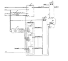
本形態は図1に示すように、メモリチップセレクト生成部101と、メモリ102と、チップセレクト生成部103と、初期化監視部104と、初期化解除信号選択部105と、データ選択部106と、タイミング調整部107とから構成されている。また、初期化監視部104には、複数のF/F141−1〜141−nが設けられている。ここで、メモリ102は、説明の便宜上、アドレスが「0」〜「n−1」であるメモリを例に挙げる。データ幅については、任意のデータ幅で良い。一般的なメモリと同様に、各アドレスによって指定されるエリアには、データが1つずつエントリー(記憶)されるようになっている。また、図1中に示す信号は説明しやすいようにすべて正論理の信号とする。
In this embodiment, as shown in FIG. 1, a memory chip
図2は、図1に示した多ビット記憶装置にて使用されるメモリ102のアドレスとエントリーとの対応付けを示す図である。
FIG. 2 is a diagram showing the correspondence between addresses and entries in the
図2に示すようにメモリ102の各アドレスに1つずつエントリーがそれぞれ対応付けられている。すなわち、アドレス「0」にエントリー1が、また、アドレス「1」にエントリー2が、また、アドレス「2」にエントリー3が、また、アドレス「n−1」にエントリーnがそれぞれ対応付けられている。実際にメモリ102には、アドレスによって指定されるエリアに、エントリー1〜nのライトデータが記憶される。
As shown in FIG. 2, one entry is associated with each address in the
メモリチップセレクト生成部101は、メモリ102にライトデータを書き込むためのアドレスと、ライトデータの書き込みが可能かどうかを示すライトイネーブルとが入力され、入力されたアドレスをデコードしてメモリに割り当てられたアドレスであるかどうかを判断し、メモリに割り当てられたアドレスであると判断され、且つ、入力されたライトイネーブルが「High」レベルである場合に、メモリチップセレクトを「High」レベルでメモリ102へ出力する。
The memory chip
メモリ102は、アドレスと、ライトデータと、クロックと、メモリチップセレクト生成部101から出力されたメモリチップセレクトとが入力され、入力されたメモリチップセレクトが「High」レベルである場合に、入力されたアドレスによって指定されたエリアにライトデータをクロックに同期して書き込む。メモリ102は一般的なクロック同期型のメモリであり、「DTI」は所定のビット幅を持つデータ入力、また、「ADD」は所定のビット幅を持つアドレス入力、また、「CS」はチップセレクト信号入力、また、「CLK」はデータの書き込み及び読み出しのトリガとなるクロック入力、また、「DTO」は所定のビット幅を持つデータ出力のための端子である。また、メモリ102は、電源投入後等の初期状態では、ライトデータが書き込まれるまでメモリリードデータが不定となるため、メモリリードデータを選択するためには、メモリ102の後段に出力タイミングを調整するための手段が必要である。
The
チップセレクト生成部103は、アドレスと、ライトイネーブルとが入力され、入力されたアドレスをデコードしてメモリに割り当てられたアドレスであるかどうかを判断し、メモリに割り当てられたアドレスであると判断され、且つ、入力されたライトイネーブルが「High」レベルである場合に、該当するアドレスのエントリーに応じたチップセレクト1〜nを「High」レベルでそれぞれ出力する。ここでは、アドレスが「0」である場合、チップセレクト1を「High」レベルに、また、アドレスが「1」である場合は、チップセレクト2を「High」レベルに、また、アドレスが「n−1」である場合は、チップセレクトnを「High」レベルにして出力する。
The chip
初期化監視部104は、設けられた複数のF/F141−1〜141−nのそれぞれが1つのアドレスと対応しており、チップセレクト生成部103から該当するアドレスのエントリーに対して出力されたチップセレクト1〜nが、F/F141−1〜141−nのそれぞれに入力され、入力されたチップセレクト1〜nが「High」レベルである場合、初期化解除信号1〜nを「High」レベルでそれぞれ出力する。また、F/F141−1〜141−nは、一般的な非同期リセット型のフリップフロップであり、「D」はデータ入力、また、「CS」はイネーブル信号入力、また、「CLK」は動作するために入力されるクロック入力、また、「RST」はリセット信号入力、また、「Q」はデータ出力のための端子である。
In the
初期化解除信号選択部105は、アドレスと、初期化監視部104のF/F141−1〜141−nから出力される初期化解除信号1〜nとが入力され、入力された初期化解除信号1〜nのうち1つの初期化解除信号を選択する。どの初期化解除信号を選択するかは、入力されたアドレスに基づいて決定される。ここでは、アドレスが「0」である場合、初期化解除信号1を、また、アドレスが「1」である場合は、初期化解除信号2を、また、アドレスが「n−1」の場合は、初期化解除信号nを選択する。
The initialization cancellation
タイミング調整部107は、初期解除信号選択部105から出力された初期化解除信号の出力タイミングを調整する。上述したように、本形態におけるメモリ102は、電源投入後等の初期状態では、ライトデータが書き込まれるまでメモリリードデータが不定となるため、メモリリードデータの有効データを選択するための初期化解除信号の出力タイミングを調整するタイミング調整部107が設けられている。
The
データ選択部106は、メモリ102から出力されたメモリリードデータと、予め設定された初期値と、タイミング調整部107から出力された初期化解除信号とが入力され、入力された初期解除信号に基づいて、初期値とメモリリードデータとのどちらかを選択してリードデータとして出力する。つまり、初期値とメモリリードデータとを入力として、タイミング調整部107から出力された初期化解除信号をセレクト制御信号とした2入力1出力のセレクタと同様に動作する。
The
また、図1に示したチップセレクト1〜nは、図2に示したエントリー1〜nにアクセス可能な場合に「High」レベルになる信号であり、また、図1に示した初期化解除信号1〜nについては、図2に示したエントリー1〜nの初期化解除を行う信号である。
The chip select 1 to n shown in FIG. 1 is a signal that becomes “High” level when the
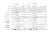
以下に、図1に示した多ビット記憶装置における各信号のタイミングについて説明する。 The timing of each signal in the multi-bit storage device shown in FIG. 1 will be described below.
図3は、図1に示した多ビット記憶装置における各信号のタイミングを示すタイムチャートである。 FIG. 3 is a time chart showing the timing of each signal in the multi-bit storage device shown in FIG.
まず、多ビット記憶装置に入力されているリセットが解除された後(タイムスロットT1)、アドレス「0」及びライトデータ「A」が入力され、ライトイネーブルが「High」レベルで入力されると、メモリチップセレクト生成部101にて入力されたアドレスがメモリ102のアドレスであると判断され、且つ、入力されたライトイネーブルが「High」レベルであるため、メモリチップセレクトが「High」レベルとなって出力される。同時に、チップセレクト生成部103にて、入力されたアドレスがデコードされることによりエントリー1のものであることが判断され、且つ、入力されたライトイネーブルが「High」レベルであるため、初期化監視部104のF/F141−1へ出力するチップセレクト1が「High」レベルに設定されて出力される(タイムスロットT2)。
First, after the reset input to the multi-bit storage device is released (time slot T1), when the address “0” and the write data “A” are input and the write enable is input at the “High” level, Since the address input by the memory chip
タイムスロットT2にてチップセレクト1が「High」レベルに設定されて出力されると、チップセレクト1がイネーブル信号入力となっているF/F141−1の「CS」に入力され、F/F141−1が動作可能状態となり、入力データとして「D」に接続されている「High」レベルの固定信号が「CLK」に入力されているクロックで打ち抜かれて、初期化解除信号1が「High」レベル信号となって「Q」から出力される(タイムスロットT3)。
When chip select 1 is set to “High” level and output at time slot T2, chip select 1 is input to “CS” of F / F 141-1, which is an enable signal input, and F / F 141- 1 becomes operable, and a fixed signal of “High” level connected to “D” as input data is punched out by the clock input to “CLK”, and the
一方、メモリ102へのライト動作においては、メモリチップセレクトが「High」となった次のクロックの立ち上がりであるタイムスロットT3にて、メモリ102に入力されたアドレス「0」によって指定されたエリアにライトデータ「A」が書き込まれる。その後、ライトイネーブルが「Low」レベルになると(タイムスロットT4)、書き込まれたデータ「A」は次のクロックの立ち上がりからメモリリードデータとして「DTO」から出力され、また、F/F141−1から出力された初期解除信号1は、メモリリードデータの出力タイミングと合わせるために、タイミング調整部107にてタイミングを調整されて出力される(タイムスロットT5)。本形態では、1クロック分遅らされて出力される。
On the other hand, in the write operation to the
そして、データ選択部106にて、予め設定されている初期値と、メモリ102から出力されたメモリリードデータと、タイミング調整部107から出力された初期化解除信号とが入力され、初期化解除信号が「Low」レベルである場合、初期値が選択され、また初期化解除信号が「High」レベルである場合は、メモリリードデータが選択される。そして、選択された信号がリードデータとしてデータ選択部106から出力される。
Then, the
タイムスロットT5までは、タイミング調整部107の出力が「Low」レベルであるため、データ選択部106にて初期値が選択されて出力される。一方、タイムスロットT5以降は、タイミング調整部107の出力が「High」レベルであるため、データ選択部106にてメモリリードデータが選択されて出力される。
Until the time slot T5, since the output of the
その後、再度リセットが入力されると、初期化監視部104内のF/F141−1〜141−nがリセットされ、初期化解除信号1〜nが「Low」レベルとなり、「Low」レベルとなった初期化解除信号が、タイミング調整部107にて1クロック遅らされると、そのタイミングから、データ選択部106にて初期値が選択されて出力される(タイムスロットT6)。
After that, when reset is input again, the F / Fs 141-1 to 141-n in the
その後、リセットが解除され(タイムスロットT7)、アドレス「1」及びライトデータ「B」が入力され、ライトイネーブルが「High」レベルで入力されると、メモリチップセレクト生成部101にて入力されたアドレスがメモリ102のアドレスであると判断され、且つ、入力されたライトイネーブルが「High」レベルであるため、メモリチップセレクトが「High」レベルとなって出力される。同時に、チップセレクト生成部103にて、入力されたアドレスがデコードされることによりエントリー2のものであることが判断され、且つ、入力されたライトイネーブルが「High」レベルであるため、初期化監視部104のF/F141−2へ出力するチップセレクト2が「High」レベルに設定されて出力される(タイムスロットT8)。
Thereafter, the reset is released (time slot T7), the address “1” and the write data “B” are input, and the write enable is input at the “High” level. Since the address is determined to be the address of the
タイムスロットT8にてチップセレクト2が「High」レベルに設定されて出力されると、チップセレクト2がイネーブル信号入力となっているF/F141−2の「CS」に入力され、F/F141−2が動作可能状態となり、入力データとして「D」に接続されている「High」レベルの固定信号が「CLK」に入力されているクロックで打ち抜かれて、初期化解除信号2が「High」レベルとなって「Q」から出力される(タイムスロットT9)。
When the chip select 2 is set to “High” level and output at the time slot T8, the chip select 2 is input to “CS” of the F / F 141-2 which is an enable signal input, and the F / F 141- 2 becomes operable, and the “High” level fixed signal connected to “D” as input data is punched out by the clock input to “CLK”, and the
一方、メモリ102へのライト動作においては、メモリチップセレクトが「High」となった次のクロックの立ち上がりであるタイムスロットT9にて、メモリ102に入力されたアドレス「1」」によって指定されたエリアにライトデータ「B」が書き込まれる。その後、ライトイネーブルが「Low」レベルになると(タイムスロットT10)、書き込まれたデータ「B」は次のクロックの立ち上がりからメモリリードデータとして「DTO」から出力され、また、F/F141−2から出力された初期解除信号2は、メモリリードデータの出力タイミングと合わせるために、タイミング調整部107にてタイミングを調整されて出力される(タイムスロットT11)。ここでは、初期解除信号1のときと同様に、1クロック分遅らされて出力される。
On the other hand, in the write operation to the
そして、データ選択部106にて、予め設定されている初期値と、メモリ102から出力されたメモリリードデータと、タイミング調整部107から出力された初期化解除信号とが入力され、初期化解除信号が「Low」レベルである場合、初期値が選択され、また初期化解除信号が「High」レベルである場合は、メモリリードデータが選択される。そして、選択された信号がリードデータとしてデータ選択部106から出力される。
Then, the
タイムスロットT11までは、タイミング調整部107の出力が「Low」レベルであるため、データ選択部106にて初期値が選択されて出力される。一方、タイムスロットT11以降は、タイミング調整部107の出力が「High」レベルであるため、データ選択部106にてメモリリードデータが選択されて出力される。
Until the time slot T11, since the output of the
このように、多ビット記憶装置のリセット後、メモリ102内のあるアドレスによって指定されたエリアへのライトデータの書き込み処理が終了するまでは、予め設定された初期値が出力され、また、メモリ102内のあるアドレスによって指定されたエリアへのライトデータの書き込み処理が終了した後は、メモリ102に書き込まれたライトデータが出力されることとなる。
As described above, after the reset of the multi-bit storage device, a preset initial value is output until the write processing of the write data to the area designated by a certain address in the
なお、データ選択部106に入力される初期値は、各エントリー毎に固有の値に設定されても良い。
Note that the initial value input to the
図4は、図1に示したデータ選択部106に入力される初期値が、各エントリー毎に固有に設定された値が使用される場合の多ビット記憶装置の実施の一形態を示す図である。
FIG. 4 is a diagram showing an embodiment of the multi-bit storage device in the case where the initial value input to the
本形態は図4に示すように、図1に示した形態に初期値選択部110が追加された形態となっている。
As shown in FIG. 4, the present embodiment is a form in which an initial
初期値選択部110は、各エントリーに対応付けられた初期値1〜nと、アドレスとが入力され、入力されたアドレスに基づいて初期値1〜nのうち1つを選択する。つまり、アドレスが「0」である場合、初期値1を、また、アドレスが「1」である場合は、初期値2を、また、アドレスが「n−1」である場合は、初期値nを選択する。そして、選択された初期値をデータ選択部106へ出力する。その他の構成及び動作については、図1に示した形態と同様である。
The initial
また、上述した初期値については、メモリ102の未使用エリアや、他にレジスタを設けてその中に予め格納されてあっても良い。
Further, the above-described initial value may be stored in advance in an unused area of the
101 メモリチップセレクト生成部
102 メモリ
103 チップセレクト生成部
104 初期値監視部
105 初期化解除信号選択部
106 データ選択部
107 タイミング調整部
110 初期値選択部
141−1〜141−n F/F
DESCRIPTION OF
Claims (4)
前記多ビット記憶装置のリセット後、メモリ内の、外部から入力されたアドレスによって指定されたエリアへの外部から入力されたデータの書き込み処理が終了するまでは無効となり、該データの書き込み処理が終了した後は有効となる初期化解除信号を生成し、前記初期化解除信号が無効である場合、予め設定された初期値を選択して出力し、また、前記初期化解除信号が有効である場合は、前記メモリから読み出されたデータを選択して出力する多ビット記憶装置。 A multi-bit storage device for storing data composed of a plurality of bits,
After resetting the multi-bit storage device, it becomes invalid until the processing of writing data input from the outside to the area specified by the address input from the outside in the memory is completed, and the processing of writing the data ends. When the initialization cancellation signal that becomes valid is generated and the initialization cancellation signal is invalid, a preset initial value is selected and output, and the initialization cancellation signal is valid Is a multi-bit storage device that selects and outputs data read from the memory.
前記データを記憶するメモリと、
前記多ビット記憶装置のリセット後、前記メモリ内の、外部から入力されたアドレスによって指定されたエリアへの外部から入力されたデータの書き込み処理が終了するまでは無効となり、該データの書き込み処理が終了した後は有効となる初期化解除信号を生成する初期化監視手段と、
前記初期化解除信号が無効である場合、予め設定された初期値を選択して出力し、また、前記初期化解除信号が有効である場合は、前記メモリから読み出されたデータを選択して出力するデータ選択手段とを有することを特徴とする多ビット記憶装置。 The multi-bit storage device according to claim 1.
A memory for storing the data;
After resetting of the multi-bit memory device, in said memory, until the writing process of data input from the outside to the specified area by the address inputted from the outside is finished becomes invalid, writing process of the data Initialization monitoring means for generating an initialization cancellation signal that becomes valid after the completion,
When the initialization release signal is invalid, a preset initial value is selected and output, and when the initialization release signal is valid, the data read from the memory is selected. And a data selection means for outputting the data.
前記初期化監視手段は、1つの前記アドレスにつき1つのフリップフロップによって初期化解除信号を生成することを特徴とする多ビット記憶装置。 The multi-bit storage device according to claim 2.
The multi-bit storage device according to claim 1, wherein the initialization monitoring means generates an initialization cancellation signal by one flip-flop per one address.
前記多ビット記憶装置のリセット後、メモリ内の、外部から入力されたアドレスによって指定されたエリアへの外部から入力されたデータの書き込み処理が終了するまでは無効となり、該データの書き込み処理が終了した後は有効となる初期化解除信号を生成する処理と、
前記初期化解除信号が無効である場合、予め設定された初期値を選択して出力する処理と、
前記初期化解除信号が有効である場合は、前記メモリから読み出されたデータを選択して出力する処理とを有する多ビット記憶方法。 A multi-bit storage method in a multi-bit storage device for storing data composed of a plurality of bits,
After resetting the multi-bit storage device, it becomes invalid until the processing of writing data input from the outside to the area specified by the address input from the outside in the memory is completed, and the processing of writing the data ends. Processing to generate an initialization release signal that becomes valid after
When the initialization cancellation signal is invalid, a process of selecting and outputting a preset initial value;
And a process of selecting and outputting data read from the memory when the initialization cancellation signal is valid.
Priority Applications (1)
| Application Number | Priority Date | Filing Date | Title |
|---|---|---|---|
| JP2005335528A JP4829598B2 (en) | 2005-11-21 | 2005-11-21 | Multi-bit storage device and multi-bit storage method |
Applications Claiming Priority (1)
| Application Number | Priority Date | Filing Date | Title |
|---|---|---|---|
| JP2005335528A JP4829598B2 (en) | 2005-11-21 | 2005-11-21 | Multi-bit storage device and multi-bit storage method |
Publications (2)
| Publication Number | Publication Date |
|---|---|
| JP2007141035A JP2007141035A (en) | 2007-06-07 |
| JP4829598B2 true JP4829598B2 (en) | 2011-12-07 |
Family
ID=38203801
Family Applications (1)
| Application Number | Title | Priority Date | Filing Date |
|---|---|---|---|
| JP2005335528A Active JP4829598B2 (en) | 2005-11-21 | 2005-11-21 | Multi-bit storage device and multi-bit storage method |
Country Status (1)
| Country | Link |
|---|---|
| JP (1) | JP4829598B2 (en) |
Families Citing this family (1)
| Publication number | Priority date | Publication date | Assignee | Title |
|---|---|---|---|---|
| TWI443658B (en) * | 2008-12-18 | 2014-07-01 | Mosaid Technologies Inc | Semiconductor device with main memory unit and auxiliary memory unit requiring preset operation |
Family Cites Families (4)
| Publication number | Priority date | Publication date | Assignee | Title |
|---|---|---|---|---|
| JPH03147033A (en) * | 1989-11-01 | 1991-06-24 | Oki Electric Ind Co Ltd | Data base control system |
| JPH05324452A (en) * | 1992-05-27 | 1993-12-07 | Nec Ic Microcomput Syst Ltd | External memory interface circuit |
| JPH0736759A (en) * | 1993-07-15 | 1995-02-07 | Hitachi Ltd | Semiconductor filing system |
| JP2000267925A (en) * | 1999-03-19 | 2000-09-29 | Canon Inc | Memory control device |
-
2005
- 2005-11-21 JP JP2005335528A patent/JP4829598B2/en active Active
Also Published As
| Publication number | Publication date |
|---|---|
| JP2007141035A (en) | 2007-06-07 |
Similar Documents
| Publication | Publication Date | Title |
|---|---|---|
| JP6224401B2 (en) | Semiconductor memory | |
| CN107408406B (en) | Method and apparatus for reducing command shifters | |
| JP5096131B2 (en) | Semiconductor memory device | |
| US10223110B2 (en) | Central processing unit and arithmetic unit | |
| KR0155177B1 (en) | Output circuit of semiconductor memory | |
| JP3756231B2 (en) | Synchronous semiconductor memory device | |
| JP4419074B2 (en) | Semiconductor memory device | |
| JP7035361B2 (en) | Storage device, register file circuit and storage device control method | |
| JP4829598B2 (en) | Multi-bit storage device and multi-bit storage method | |
| JP2003044303A (en) | Computer system | |
| KR100712546B1 (en) | Circuit and method for generating write data mask signal in synchronous semiconductor memory device | |
| JP4757582B2 (en) | Data transfer operation end detection circuit and semiconductor memory device including the same | |
| JP2003208788A (en) | Buffer by two ports memory | |
| JP2853612B2 (en) | Semiconductor storage device | |
| JP3882628B2 (en) | Memory control device and serial memory | |
| JP2009230434A (en) | Reset circuit | |
| US6175518B1 (en) | Remote register hierarchy accessible using a serial data line | |
| KR100902048B1 (en) | Circuit for receiving address of semiconductor apparatus | |
| JP2002117683A (en) | Clock-switching circuit and memory device having the circuit | |
| JPH10340596A (en) | Data storage device and semiconductor memory | |
| US7184357B2 (en) | Decoding circuit for memory device | |
| WO2014097957A1 (en) | Semiconductor device | |
| JP2697772B2 (en) | Information processing device | |
| JP2818563B2 (en) | Synchronous memory | |
| US20050223160A1 (en) | Memory controller |
Legal Events
| Date | Code | Title | Description |
|---|---|---|---|
| A621 | Written request for application examination |
Free format text: JAPANESE INTERMEDIATE CODE: A621 Effective date: 20080918 |
|
| A131 | Notification of reasons for refusal |
Free format text: JAPANESE INTERMEDIATE CODE: A131 Effective date: 20110629 |
|
| A521 | Written amendment |
Free format text: JAPANESE INTERMEDIATE CODE: A523 Effective date: 20110809 |
|
| TRDD | Decision of grant or rejection written | ||
| A01 | Written decision to grant a patent or to grant a registration (utility model) |
Free format text: JAPANESE INTERMEDIATE CODE: A01 Effective date: 20110907 |
|
| A01 | Written decision to grant a patent or to grant a registration (utility model) |
Free format text: JAPANESE INTERMEDIATE CODE: A01 |
|
| A61 | First payment of annual fees (during grant procedure) |
Free format text: JAPANESE INTERMEDIATE CODE: A61 Effective date: 20110916 |
|
| FPAY | Renewal fee payment (event date is renewal date of database) |
Free format text: PAYMENT UNTIL: 20140922 Year of fee payment: 3 |
|
| R150 | Certificate of patent or registration of utility model |
Ref document number: 4829598 Country of ref document: JP Free format text: JAPANESE INTERMEDIATE CODE: R150 Free format text: JAPANESE INTERMEDIATE CODE: R150 |
|
| S111 | Request for change of ownership or part of ownership |
Free format text: JAPANESE INTERMEDIATE CODE: R313111 |
|
| R350 | Written notification of registration of transfer |
Free format text: JAPANESE INTERMEDIATE CODE: R350 |