JP4826348B2 - Method for producing multilayer ceramic electronic component with protruding electrodes - Google Patents
Method for producing multilayer ceramic electronic component with protruding electrodes Download PDFInfo
- Publication number
- JP4826348B2 JP4826348B2 JP2006160283A JP2006160283A JP4826348B2 JP 4826348 B2 JP4826348 B2 JP 4826348B2 JP 2006160283 A JP2006160283 A JP 2006160283A JP 2006160283 A JP2006160283 A JP 2006160283A JP 4826348 B2 JP4826348 B2 JP 4826348B2
- Authority
- JP
- Japan
- Prior art keywords
- layer
- unsintered
- ceramic
- multilayer ceramic
- electronic component
- Prior art date
- Legal status (The legal status is an assumption and is not a legal conclusion. Google has not performed a legal analysis and makes no representation as to the accuracy of the status listed.)
- Expired - Fee Related
Links
Images


Description
本願発明は、多層セラミック電子部品の製造方法に関し、詳しくは、表面に突起状電極が配設された構造を有する、突起状電極付き多層セラミック電子部品の製造方法に関する。 The present invention relates to a method for manufacturing a multilayer ceramic electronic component, and more particularly to a method for manufacturing a multilayer ceramic electronic component with protruding electrodes having a structure in which protruding electrodes are disposed on the surface.
近年、エレクトロニクス分野における電子部品の性能は著しく向上しており、大型コンピュータ、移動通信端末、パーソナルコンピュータなどの情報処理装置における情報処理速度の高速化、装置の小型化、多機能化に貢献している。 In recent years, the performance of electronic components in the electronics field has improved remarkably, contributing to faster information processing speeds, smaller devices, and more functions in information processing devices such as large computers, mobile communication terminals, and personal computers. Yes.
このような電子部品の一つとして、VLSI、ULSIなどの半導体デバイスをセラミック基板上に複数実装したマルチチップモジュール(MCM)が挙げられる。このようなモジュールにおいては、LSIの実装密度を高め、各LSI間を電気的に確実に接続するために、配線導体を3次元的に配置したセラミック多層基板が広く用いられている。 As one of such electronic components, there is a multichip module (MCM) in which a plurality of semiconductor devices such as VLSI and ULSI are mounted on a ceramic substrate. In such a module, a ceramic multilayer substrate in which wiring conductors are three-dimensionally arranged is widely used in order to increase the mounting density of LSIs and to electrically connect the LSIs reliably.
このセラミック多層基板は、複数のセラミック層を積層することにより形成されており、その表面や内部に回路構成用の配線導体を備えたものであるが、携帯電話や自動車用無線通信機器などに代表される移動通信端末においては、高機能高密度実装の要求も厳しくなり、さらなる小型化が求められている。また、その用途などから、セラミック多層基板を用いた製品の耐衝撃性に対する要求はますます高まっている。 This ceramic multilayer substrate is formed by laminating a plurality of ceramic layers, and is provided with wiring conductors for circuit configuration on the surface or inside thereof, but is representative of cellular phones, automobile wireless communication devices, etc. In such mobile communication terminals, the demand for high-functional and high-density mounting has become strict, and further miniaturization is required. In addition, the demand for impact resistance of products using ceramic multilayer substrates is increasing due to their use.
ところで、このようなセラミック多層基板に代表される多層セラミック電子部品には、図8に示すように、セラミック層71,72,73,面内導体74,ビアホール75に充填されたビアホール導体76などからなる導体パターン51が配設された多層セラミック素体52と、多層セラミック素体52の第1主面53に、導体パターン51と接続するように配設されたバンプ(突起状電極)54を備えた構造を有するものがある(特許文献1参照)。
By the way, multilayer ceramic electronic components represented by such a ceramic multilayer substrate include
この多層セラミック電子部品は、以下の方法で製造されている。図9を参照しつつ、この多層セラミック電子部品について説明する。
(1)面内導体74となる導電性ペースト81を表面に印刷し、および/またはビアホール導体76となる導電性ペースト82を貫通孔(ビアホール)75に充填したセラミックグリーンシート80を用意し、所定の順序および態様となるように積層する。
This multilayer ceramic electronic component is manufactured by the following method. The multilayer ceramic electronic component will be described with reference to FIG.
(1) A ceramic
(2)そして、積層体の上面側に、セラミックグリーンシート80が焼結する温度では実質的に焼結しないセラミック材料からなり、ビアホール75にバンプ54を形成するための導電性ペースト83が充填されたセラミックグリーンシート91を積層する。
(2) The upper surface of the laminate is filled with a
(3)さらに、上下両主面側に、セラミックグリーンシート80が焼結する温度では実質的に焼結しない難焼結性のセラミック材料からなるセラミックグリーンシート92,93を、焼成工程におけるセラミックグリーンシート80の、平面方向の収縮を抑制するための収縮抑制層として積層する。
(3) Furthermore, ceramic
(4)それから、全体を、セラミックグリーンシート80は焼結するが、ビアホール75にバンプ形成用の導電性ペースト83が充填されたセラミックグリーンシート91および収縮抑制層であるセラミックグリーンシート92,93は焼結しない温度で焼成する。
(4) Then, although the ceramic
(5)その後、未焼結のセラミックグリーンシート(収縮抑制層)92,93、および、未焼結のセラミックグリーンシート91を除去する。
これにより、図8に示すような構造を有する多層セラミック電子部品が得られる。
(5) Thereafter, the unsintered ceramic green sheets (shrinkage suppression layers) 92 and 93 and the unsintered ceramic
Thereby, a multilayer ceramic electronic component having a structure as shown in FIG. 8 is obtained.
しかしながら、上記従来の多層セラミック電子部品の製造方法においては、未焼結のセラミックグリーンシート(収縮抑制層)92,93、および、未焼結のセラミックグリーンシート91の除去工程が必要である。
そして、平板状の収縮抑制層92,93の除去は比較的容易であるが、バンプ形成用のセラミックグリーンシート91を除去する場合、このセラミックグリーンシート91には焼結したバンプが形成されているため、刷毛による機械的な除去作業や、超音波洗浄による除去作業などが必要で、多大な手間がかかるばかりでなく、このバンプ形成用のセラミックグリーンシート91の除去工程で、バンプ54が脱落してしまう場合があり、信頼性が低いという問題点がある。
なお、バンプの平面断面積が小さくなり、細くなるほど、脱落のおそれは大きくなる。
However, in the conventional method for manufacturing a multilayer ceramic electronic component, a step of removing the unsintered ceramic green sheets (shrinkage suppression layers) 92 and 93 and the unsintered ceramic
The removal of the plate-like
Note that the smaller the plane cross-sectional area of the bump is, the smaller the bump is, the greater the risk of falling off.
また、高密度に配設したバンプ間、特に、バンプの根元付近は、バンプ形成用のセラミックグリーンシートの除去が困難で、基板側、すなわち、焼結したセラミックグリーンシート側から拡散してくるガラス成分などにより、実質的には未焼結であっても、バンプ形成用のセラミックシートが部分的に、基板側に固着されてしまうという問題がある。 Also, it is difficult to remove the ceramic green sheet for bump formation between the bumps arranged at high density, especially near the base of the bump, and the glass diffused from the substrate side, that is, the sintered ceramic green sheet side. There is a problem that the ceramic sheet for bump formation is partially fixed to the substrate side even if it is substantially unsintered due to components or the like.
また、バンプ54の高さはバンプ形成用の難焼結性のセラミックグリーンシート91の厚みに対応するため、焼成時の収縮抑制をバンプ形成用の難焼結性のセラミックグリーンシート91に依存する場合、バンプ54の高さに対応するバンプ形成用の難焼結性のセラミックグリーンシート91の厚みでは十分な収縮抑制効果が得られない場合には、バンプ形成用の難焼結性のセラミックグリーンシート91の表面にさらに、収縮抑制用の難焼結性セラミックグリーンシートを積層することが必要となり、製造工程が複雑になるという問題点がある。
Further, since the height of the
なお、一方の面についてのみ、収縮抑制用の難焼結性セラミックグリーンシートを厚くすると、焼成後の多層セラミック素体の反りなどの変形要因となるため、一方の面について、収縮抑制用の難焼結性セラミックグリーンシートを厚くした場合には、必然的に他方の面についても、収縮抑制用の難焼結性セラミックグリーンシートの厚みを厚くすることが必要になり、収縮抑制層用の材料の使用量増大、製造工程の複雑化などを招くという問題点がある。 It should be noted that increasing the thickness of the non-sinterable ceramic green sheet for suppressing shrinkage on only one surface may cause deformation factors such as warping of the multilayer ceramic body after firing. When the sinterable ceramic green sheet is thickened, it is inevitably necessary to increase the thickness of the non-sinterable ceramic green sheet for suppressing shrinkage on the other side as well. There is a problem in that the amount of use increases and the manufacturing process becomes complicated.
さらに、上記従来の多層セラミック電子部品の製造方法によれば、収縮抑制用の難焼結性セラミックグリーンシートは多層セラミック素体の主面全体に配設することが必要であることから、外部導体(表面電極)上の難焼結性セラミックグリーンシートの除去が不十分になりやすく、表面処理の不良や実装部品の実装不良が発生しやすいという問題点がある。 Furthermore, according to the above-described conventional method for producing a multilayer ceramic electronic component, the non-sinterable ceramic green sheet for suppressing shrinkage needs to be disposed on the entire main surface of the multilayer ceramic body. There is a problem in that removal of the hardly sinterable ceramic green sheet on the (surface electrode) tends to be insufficient, and surface treatment defects and mounting component mounting defects are likely to occur.
さらに、多層セラミック素体自体も収縮挙動を示すため、バンプ形成用の難焼結性セラミックグリーンシートと多層セラミック素体間に滑りが生じた場合には、多層セラミック素体に高精度に接続することが必要なバンプ部に位置ずれが生じ、断線不良が発生するというような問題点がある。
本願発明は、上記課題を解決するものであり、表面に突起状電極を備えた多層セラミック電子部品を、複雑な製造工程を必要とせずに、効率よく製造することが可能な突起状電極付き多層セラミック電子部品の製造方法を提供することを目的とする。 The present invention solves the above-mentioned problems, and a multilayer with a protruding electrode that can efficiently manufacture a multilayer ceramic electronic component having a protruding electrode on its surface without requiring a complicated manufacturing process. An object of the present invention is to provide a method for manufacturing a ceramic electronic component.
上記課題を解決するために、本願発明(請求項1)の突起状電極付き多層セラミック電子部品の製造方法は、
未焼結セラミック基材層と、前記未焼結セラミック基材層の平面方向の収縮を抑制するための収縮抑制層とが積層され、未焼結導体パターンを備えた未焼結多層セラミック素体の第1主面に、前記未焼結セラミック基材層の焼成温度において少なくとも主要部が消失する消失層を介して、未焼結突起状電極を有する補助層が、前記未焼結多層セラミック素体の未焼結導体パターンと前記未焼結突起状電極とが当接するような態様で配置された積層体を形成する工程と、
前記積層体を、前記未焼結セラミック基材層および前記未焼結突起状電極が焼結する温度で焼成することにより、前記消失層の少なくとも主要部を消失させるとともに、前記未焼結セラミック基材層および前記未焼結突起状電極を焼結させる工程と
を具備することを特徴としている。
In order to solve the above-mentioned problems, a method for producing a multilayer ceramic electronic component with protruding electrodes according to the present invention (Claim 1)
A non-sintered multilayer ceramic body comprising a non-sintered ceramic base material layer and a non-sintered ceramic base material layer having a non-sintered conductor pattern, wherein a non-sintered ceramic base material layer and a shrinkage suppression layer for suppressing shrinkage in a planar direction are laminated. An auxiliary layer having unsintered protruding electrodes is formed on the first main surface of the unsintered multilayer ceramic element through a disappearing layer in which at least a main part disappears at the firing temperature of the unsintered ceramic base layer. Forming a laminated body arranged in such a manner that the unsintered conductor pattern of the body and the unsintered protruding electrode are in contact with each other;
The laminate is fired at a temperature at which the unsintered ceramic base layer and the unsintered protruding electrode sinter, thereby eliminating at least the main part of the disappearing layer and the unsintered ceramic base. And a step of sintering the material layer and the unsintered protruding electrode.
また、請求項2の突起状電極付き多層セラミック電子部品の製造方法は、請求項1の発明の構成において、前記補助層が、前記未焼結セラミック基材層を構成するセラミックの焼結温度では実質的に焼結しないセラミック粉末を主成分とするセラミック補助層であり、前記焼成の後、実質的に未焼結の前記セラミック補助層を除去する工程をさらに備えることを特徴としている。 According to a second aspect of the present invention, there is provided a method for producing a multilayer ceramic electronic component with protruding electrodes, wherein the auxiliary layer is at a sintering temperature of the ceramic constituting the unsintered ceramic base layer. A ceramic auxiliary layer mainly composed of a ceramic powder that is not substantially sintered, and further comprising a step of removing the substantially unsintered ceramic auxiliary layer after the firing.
また、請求項3の突起状電極付き多層セラミック電子部品の製造方法は、請求項1または2の発明の構成において、焼結させた前記突起状電極の上側端面に表面実装型電子部品を搭載する工程をさらに備えることを特徴としている。
According to a third aspect of the present invention, there is provided a method for manufacturing a multilayer ceramic electronic component with protruding electrodes, wherein the surface-mounted electronic component is mounted on the upper end face of the sintered protruding electrode in the configuration of the invention of
また、請求項4の突起状電極付き多層セラミック電子部品の製造方法は、請求項1〜3のいずれかの発明の構成において、前記補助層および前記消失層を、前記未焼結多層セラミック素体の前記第1主面の一部領域に配置することを特徴としている。 According to a fourth aspect of the present invention, there is provided a method for producing a multilayer ceramic electronic component with protruding electrodes, wherein the auxiliary layer and the disappearing layer are formed of the unsintered multilayer ceramic body in the configuration of any one of the first to third aspects. It arrange | positions to a partial area | region of said 1st main surface.
また、請求項5の突起状電極付き多層セラミック電子部品の製造方法は、請求項1〜4のいずれかの発明の構成において、前記未焼結多層セラミック素体の前記第1主面側に、前記収縮抑制層を配設することを特徴としている。
Moreover, the manufacturing method of the multilayer ceramic electronic component with a protruding electrode of
また、請求項6の突起状電極付き多層セラミック電子部品の製造方法は、請求項1〜5のいずれかの発明の構成において、前記未焼結セラミック基材層が、低温焼結セラミックを主成分とする未焼結セラミック基材層であり、前記収縮抑制層が、前記低温焼結セラミックの焼結温度では実質的に焼結しない難焼結性セラミックを主成分とする収縮抑制層であることを特徴としている。 According to a sixth aspect of the present invention, there is provided a method for producing a multilayer ceramic electronic component with protruding electrodes, wherein the unsintered ceramic base layer is mainly composed of a low-temperature sintered ceramic. The shrinkage-suppressing layer is a shrinkage-suppressing layer mainly composed of a hardly-sinterable ceramic that does not substantially sinter at the sintering temperature of the low-temperature sintered ceramic. It is characterized by.
また、請求項7の突起状電極付き多層セラミック電子部品の製造方法は、前記難焼結性セラミックを、焼成時に前記未焼結セラミック基材層からしみ出してきたガラスにより固着させることを特徴としている。 The method for producing a multilayer ceramic electronic component with protruding electrodes according to claim 7 is characterized in that the hardly sinterable ceramic is fixed by glass that has exuded from the unsintered ceramic base layer during firing. Yes.
また、請求項8の突起状電極付き多層セラミック電子部品の製造方法は、請求項1〜7のいずれかの発明の構成において、前記消失層が、前記未焼結セラミック基材層の前記焼成温度で分解または燃焼する樹脂からなる樹脂層であることを特徴としている。
Moreover, the manufacturing method of the multilayer ceramic electronic component with a protruding electrode of
また、請求項9の突起状電極付き多層セラミック電子部品の製造方法は、請求項1〜8のいずれかの発明の構成において、前記消失層上に前記補助層を設けた後、前記補助層および前記消失層を貫通する貫通孔を形成し、この貫通孔に導電性ペーストを充填した層を、前記未焼結多層セラミック素体の第1主面に積み重ねることにより前記積層体を形成することを特徴としている。
The method for producing a multilayer ceramic electronic component with protruding electrodes according to claim 9 is the structure of any one of
また、請求項10の突起状電極付き多層セラミック電子部品の製造方法は、請求項1〜9のいずれかの発明の構成において、前記補助層に複数の前記未焼結突起状電極を形成する場合において、前記補助層の、前記各未焼結突起状電極の間の位置に、前記補助層の上側主面から下側主面に至るスリットを形成しておくことを特徴としている。
The method for producing a multilayer ceramic electronic component with projecting electrodes according to claim 10 is the case where a plurality of the unsintered projecting electrodes are formed in the auxiliary layer in the configuration of any one of the inventions according to
本願発明(請求項1)の突起状電極付き多層セラミック電子部品の製造方法は未焼結セラミック基材層と、収縮抑制層とを積層した、未焼結導体パターンを備えた未焼結多層セラミック素体の第1主面に、焼成工程で少なくとも主要部が消失する消失層を介して、未焼結突起状電極を有する補助層を、未焼結多層セラミック素体の未焼結導体パターンと前記未焼結突起状電極とが当接するような態様で配置した積層体を形成し、この積層体を、未焼結セラミック基材層および未焼結突起状電極が焼結する温度で焼成して、消失層の少なくとも主要部を消失させるとともに、未焼結セラミック基材層および未焼結突起状電極を焼結させるようにしているので、焼成過程における多層セラミック素体の平面方向への収縮挙動を抑制して、従来の製造方法では問題となっていた、突起状電極の位置ずれを抑制することが可能になる。 The method for producing a multilayer ceramic electronic component with protruding electrodes according to the present invention (Claim 1) is a non-sintered multi-layer ceramic having a non-sintered conductor pattern in which a non-sintered ceramic base layer and a shrinkage suppression layer are laminated. An auxiliary layer having an unsintered protruding electrode is formed on the first main surface of the element body via a disappearing layer in which at least the main part disappears in the firing step, and the unsintered conductive pattern of the unsintered multilayer ceramic element body A laminated body is formed so as to be in contact with the unsintered protruding electrode, and the laminated body is fired at a temperature at which the unsintered ceramic substrate layer and the unsintered protruding electrode are sintered. In addition, at least the main part of the disappearing layer disappears, and the unsintered ceramic base layer and the unsintered protruding electrode are sintered, so that the shrinkage of the multilayer ceramic body in the plane direction during the firing process Suppress the behavior, make the conventional Has been a problem in the process, it is possible to suppress the positional displacement of the protruding electrodes.
また、多層セラミック素体に収縮抑制層を配設することにより、多層セラミック素体の一方の主面側にのみに、突起状電極の形成のための補助層を設けた場合にも、焼成工程における多層セラミック素体の変形(反りなど)を抑制することが可能になる。 In addition, even when an auxiliary layer for forming the protruding electrode is provided only on one main surface side of the multilayer ceramic body by disposing the shrinkage suppression layer on the multilayer ceramic body, the firing step It is possible to suppress the deformation (warping, etc.) of the multilayer ceramic body.
多層セラミック素体を構成する各セラミック基材層間の適切な位置に収縮抑制層を配置することにより、多層セラミック素体の収縮挙動を確実に抑制することが可能となり、突起状電極の位置ずれ、詳しくは、突起状電極と、多層セラミック素体に配設された突起状電極が接続されるべき導体パターン(接続電極)との位置ずれの発生を抑制、防止することができるようになる。 By disposing the shrinkage suppression layer at an appropriate position between the ceramic base layers constituting the multilayer ceramic body, it becomes possible to reliably suppress the shrinkage behavior of the multilayer ceramic body, and the positional deviation of the protruding electrodes, Specifically, it is possible to suppress and prevent the occurrence of misalignment between the protruding electrode and the conductor pattern (connection electrode) to which the protruding electrode disposed on the multilayer ceramic body is to be connected.
また、突起状電極が接続される未焼結多層セラミック素体の未焼結導体パターンは、未焼結多層セラミック素体に配設された回路用の未焼結導体パターンの一部であってもよく、また、突起状電極を接続する目的で配設された、ビアホール導体などの接続用電極であってもよい。また、この接続用電極は上記の回路用の導体パターンと接続されていてもよい。 Further, the unsintered conductive pattern of the unsintered multilayer ceramic body to which the protruding electrodes are connected is a part of the unsintered conductor pattern for the circuit disposed on the unsintered multilayer ceramic body. Alternatively, it may be a connection electrode such as a via-hole conductor disposed for the purpose of connecting the protruding electrode. Further, the connection electrode may be connected to the circuit conductor pattern.
なお、本願発明においては、補助層として、例えば、難焼結性のセラミック粉末を主成分とするセラミックグリーンシートなどが好ましい例として挙げられるが、その他にも、例えば、樹脂シートなどを用いることも可能である。 In the present invention, as the auxiliary layer, for example, a ceramic green sheet mainly composed of a hardly sinterable ceramic powder can be cited as a preferred example. In addition, for example, a resin sheet or the like can be used. Is possible.
また、請求項2の突起状電極付き多層セラミック電子部品の製造方法のように、請求項1の発明の構成において、補助層を、未焼結セラミック基材層を構成するセラミックの焼結温度では実質的に焼結しないセラミック粉末を主成分とするセラミック補助層とし、焼成後に、実質的に未焼結のセラミック補助層を除去するようにした場合、消失層が焼成工程で消失して、セラミック補助層と多層セラミック素体の間に隙間が形成されるとともに、セラミック補助層が焼成後にも実質的に未焼結の状態のまま残るため、大きな力を加えたりすることを必要とせずにセラミック補助層を容易に除去することが可能になり、本願発明をより実効あらしめることができる。
Moreover, like the manufacturing method of the multilayer ceramic electronic component with a protruding electrode of
なお、未焼結のセラミック補助層を除去せず、焼成後のセラミック補助層に樹脂を充填することにより、セラミック補助層を、突起状電極を備えた台座部、すなわち、表面実装型電子部品搭載用の台座部とすることも可能である。 The ceramic auxiliary layer is filled with a resin without removing the unsintered ceramic auxiliary layer, so that the ceramic auxiliary layer is mounted on the pedestal portion provided with the protruding electrodes, that is, mounted on the surface mounting type electronic component. It can also be used as a pedestal for the purpose.
また、請求項3の突起状電極付き多層セラミック電子部品の製造方法のように、請求項1または2の発明の構成において、焼結させた突起状電極の上側端面に表面実装型電子部品を搭載する工程をさらに備えることにより、突起状電極上に半導体素子などの表面実装型電子部品が搭載された、高密度実装が可能で、高機能の多層セラミック電子部品を得ることが可能になる。
Further, as in the method of manufacturing a multilayer ceramic electronic component with protruding electrodes according to
なお、本願発明において、突起状電極の上側端面に搭載される表面実装型電子部品としては、例えば、トランジスタ、IC、LSIなどが例示されるが、本願発明の突起状電極付き多層セラミック電子部品の場合、高密度に狭ギャップI/O端子を、ほぼ同一平面内に多数有する表面実装型電子部品の実装構造に適していることから、例えば、IC、LSIなどのBGA(Ball Grid Array)接続型の大型半導体素子をベアチップで搭載する場合に特に有意義である。 In the present invention, examples of the surface-mounted electronic component mounted on the upper end surface of the protruding electrode include a transistor, an IC, and an LSI, but the multilayer ceramic electronic component with the protruding electrode of the present invention is exemplified. In this case, since it is suitable for a mounting structure of a surface mounting type electronic component having a large number of narrow gap I / O terminals in a substantially same plane, for example, a BGA (Ball Grid Array) connection type such as an IC or LSI. This is particularly significant when a large semiconductor element is mounted with a bare chip.
また、本願発明においては、補助層および消失層を多層セラミック素体の全面に配置する構成に限らず、請求項4の突起状電極付き多層セラミック電子部品の製造方法のように、補助層および消失層を、未焼結多層セラミック素体の第1主面の一部領域に配置することも可能であり、多層セラミック素体の第1主面の所定の領域にのみ、突起状電極が形成された多層セラミック電子部品を効率よく製造することができる。したがって、製造可能な突起状電極付き多層セラミック電子部品の構成の自由度を向上させることが可能になる。 Further, in the present invention, the auxiliary layer and the disappearance layer are not limited to the configuration in which the auxiliary layer and the disappearance layer are disposed on the entire surface of the multilayer ceramic body. It is also possible to arrange the layer in a partial region of the first main surface of the unsintered multilayer ceramic body, and the protruding electrode is formed only in a predetermined region of the first main surface of the multilayer ceramic body. The multilayer ceramic electronic component can be efficiently manufactured. Therefore, it is possible to improve the degree of freedom in the configuration of the multilayer ceramic electronic component with protruding electrodes that can be manufactured.
なお、補助層が多層セラミック素体を構成するセラミック基材層と固着することを確実に抑制して、補助層の除去の容易さを確保する見地から、消失層を、補助層の投影面積と同等、もしくは、それよりも少し大きめに形成することが好ましい。 From the standpoint of ensuring ease of removal of the auxiliary layer by reliably suppressing the auxiliary layer from adhering to the ceramic base layer constituting the multilayer ceramic body, the disappearing layer is defined as the projected area of the auxiliary layer. It is preferable to form the same or slightly larger than that.
また、請求項5の突起状電極付き多層セラミック電子部品の製造方法のように、請求項1〜4のいずれかの発明の構成において、未焼結多層セラミック素体の第1主面側に、収縮抑制層を配設するようにした場合、突起状電極と多層セラミック素体の導体パターンとの位置ずれをより確実に抑制することが可能になり、本願発明をさらに実効あらしめることができる。
Further, as in the method for producing a multilayer ceramic electronic component with protruding electrodes according to
すなわち、未焼結の突起状電極と、未焼結多層セラミック素体を構成するセラミックとの間では、焼結収縮挙動のミスマッチングが生じるが、未焼結多層セラミック素体の表面に実質的に焼結しない収縮抑制層を位置させることにより、上記焼結収縮挙動のミスマッチングの発生を抑制して、両者間の位置ずれを抑制することが可能になる。 That is, there is a mismatch in sintering shrinkage behavior between the unsintered protruding electrode and the ceramic constituting the unsintered multilayer ceramic body, but the surface of the unsintered multilayer ceramic body is substantially By positioning the non-sintered shrinkage suppression layer, it is possible to suppress the occurrence of mismatching of the sintering shrinkage behavior and to suppress the positional deviation between the two.
また、請求項6の突起状電極付き多層セラミック電子部品の製造方法のように、請求項1〜5のいずれかの発明の構成において、未焼結セラミック基材層を、低温焼結セラミックを主成分とする未焼結セラミック基材層とし、収縮抑制層を、低温焼結セラミックの焼結温度では実質的に焼結しない難焼結性セラミックを主成分とする収縮抑制層とした場合、比較的低い温度で、平面方向の収縮を引き起こすことなく、多層セラミック素体を確実に焼成することが可能になるため、製造コストの削減を図りつつ、平面方向の寸法精度が高く、所望の特性を確実に備えた、信頼性の高い突起状電極付き多層セラミック電子部品を提供することが可能になる。
In addition, as in the method for producing a multilayer ceramic electronic component with protruding electrodes according to
また、請求項7の突起状電極付き多層セラミック電子部品の製造方法のように、収縮抑制層を構成する難焼結性セラミックを、焼成時に未焼結セラミック基材層からしみ出してきたガラスにより周囲に固着させるようにした場合、収縮抑制層が、多層セラミック素体を構成するセラミック基材層と一体化するため、焼成後に収縮抑制層を除去することが不要になり、製造工程の簡略化を図ることが可能になる。 Further, as in the method for producing a multilayer ceramic electronic component with protruding electrodes according to claim 7, the non-sinterable ceramic constituting the shrinkage suppression layer is made of glass that has exuded from the unsintered ceramic base layer during firing. When fixed to the surroundings, the shrinkage suppression layer is integrated with the ceramic base material layer that constitutes the multilayer ceramic body, so it is not necessary to remove the shrinkage suppression layer after firing, simplifying the manufacturing process. Can be achieved.
また、請求項8の突起状電極付き多層セラミック電子部品の製造方法のように、請求項1〜7のいずれかの発明の構成において、消失層を、未焼結セラミック基材層の焼成温度で分解または燃焼する樹脂からなる樹脂層とした場合、焼成工程で消失層を効率よく消失させることが可能になり、本願発明をより実効あらしめることができる。
なお、本願発明において、「分解」する樹脂とは、炭酸ガス、有機ガスなどに分解される樹脂を意味するものであって、そのような樹脂として、アクリル系樹脂などが例示される。また、「燃焼」する樹脂とは、酸素との結合により、二酸化炭素を生じせしめる樹脂を意味するものであって、そのような樹脂として、ブチラール系樹脂などが例示される。なお、「分解」と「燃焼」の両方が生じるような樹脂であってもよい。
ただし、消失層を構成する材料はこれに限らず、他の材料を用いることも可能である。
Moreover, like the manufacturing method of the multilayer ceramic electronic component with a protruding electrode of
In the present invention, the “decomposing” resin means a resin that is decomposed into carbon dioxide gas, organic gas, and the like, and examples of such a resin include acrylic resins. The “burning resin” means a resin that generates carbon dioxide by bonding with oxygen, and examples of such a resin include butyral resins. It is also possible to use a resin that causes both “decomposition” and “combustion”.
However, the material constituting the vanishing layer is not limited to this, and other materials can be used.
また、請求項9の突起状電極付き多層セラミック電子部品の製造方法のように、請求項1〜8のいずれかの発明の構成において、消失層上に補助層を設けた後、補助層および消失層を貫通する貫通孔を形成し、この貫通孔に導電性ペーストを充填した層を、未焼結多層セラミック素体の第1主面に積み重ねることにより上述の積層体を形成するようにした場合、未焼結多層セラミック素体の第1主面に突起状電極を有する補助層が配置された積層体を、効率よく形成することが可能になり、本願発明をさらに実効あらしめることができる。
In addition, as in the method for producing a multilayer ceramic electronic component with protruding electrodes according to claim 9, in the configuration of any one of
例えば、樹脂製で、消失層として機能することになるキャリアフィルム上に、難焼結性セラミック粉末を主とするセラミックスラリーを塗布し、ここに、レーザー加工などにより貫通孔を形成し、この貫通孔に導電性ペーストを充填した、いわゆるキャリアフィルム付きセラミックグリーンシートを、未焼結多層セラミック素体の第1主面に貼り付けることにより、未焼結多層セラミック素体の第1主面に、消失層(キャリアフィルム)を介して、未焼結突起状電極を有する補助層が配置された積層体を効率よく形成することが可能になる。 For example, on a carrier film that is made of resin and will function as a vanishing layer, a ceramic slurry mainly composed of a hard-to-sinter ceramic powder is applied, and through holes are formed there by laser processing or the like. A ceramic green sheet with a so-called carrier film filled with a conductive paste in the holes is attached to the first main surface of the unsintered multilayer ceramic body, to the first main surface of the unsintered multilayer ceramic body, It becomes possible to efficiently form a laminate in which an auxiliary layer having an unsintered protruding electrode is disposed via the vanishing layer (carrier film).
ただし、補助層に形成された貫通孔に充填する導電性ペーストとしては、補助層と反応する成分を含まないことが好ましく、より具体的には、ガラスフリットなどの焼結助材成分を実質的に含有していないものであることが望ましい。ただし、導電性や脱落などに悪影響を及ぼさない範囲であれば、特にその添加を妨げるものではない。
さらに、補助層との剥離性を高め、突起状電極の脱落を引き起こすことなく補助層を容易に除去できるようにする見地からは、補助層に充填する導電性ペーストとして、焼成工程で十分に収縮して、周囲の補助層との間に隙間が形成できるようなものを用いることが望ましい。
However, the conductive paste that fills the through-holes formed in the auxiliary layer preferably does not contain a component that reacts with the auxiliary layer, and more specifically, substantially contains a sintering aid component such as glass frit. It is desirable that it is not contained. However, the addition is not particularly hindered as long as it does not adversely affect conductivity, dropout, and the like.
Furthermore, from the standpoint of improving the peelability from the auxiliary layer and allowing the auxiliary layer to be easily removed without causing the protruding electrodes to drop off, the conductive layer is sufficiently contracted in the firing process as a conductive paste for filling the auxiliary layer. Thus, it is desirable to use a material that can form a gap with the surrounding auxiliary layer.
また、請求項10の突起状電極付き多層セラミック電子部品の製造方法のように、請求項1〜9のいずれかの発明の構成において、補助層に複数の前記未焼結突起状電極を形成する場合において、補助層の、各未焼結突起状電極の間の位置に、補助層の上側主面から下側主面に至るスリットを形成しておくことにより、焼成後に、実質的に未焼結で、各未焼結突起状電極の間の位置にスリットが形成された状態の補助層を、極めて容易に除去することが可能になり、本願発明をより実効あらしめることができる。 Moreover, like the manufacturing method of the multilayer ceramic electronic component with a protruding electrode of Claim 10, in the structure of any one of Claims 1-9, a plurality of said unsintered protruding electrodes are formed in the auxiliary layer. In this case, by forming a slit from the upper main surface to the lower main surface of the auxiliary layer at a position between each unsintered protruding electrode of the auxiliary layer, it is substantially unbaked after firing. As a result, the auxiliary layer in which the slits are formed at positions between the unsintered protruding electrodes can be removed very easily, and the present invention can be more effectively realized.
以下に本願発明の実施例を示して、本願発明の特徴とするところをさらに詳しく説明する。 The features of the present invention will be described in more detail below with reference to examples of the present invention.
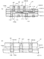
図1は、本願発明の一実施例(実施例1)にかかる多層セラミック電子部品の製造方法により製造された多層セラミック電子部品の構成を示す断面図である。
この多層セラミック電子部品は、図1に示すように、セラミック基材層101と、セラミック基材層101の平面方向の収縮を抑制するための収縮抑制層103とが積層され、かつ、所定の導体パターン102が配設された多層セラミック素体104と、多層セラミック素体104の第1主面104aに、導体パターン102と接続するように配設された、多層セラミック素体104と接する下側端面(底面)106の面積が、該底面106と対向する上側端面(上面)107の面積より大きい、台形状の形状を有する突起状電極108と、突起状電極108上に、はんだ109を介して配設された表面実装型電子部品110とを備えている。
なお、この多層セラミック電子部品において、導体パターン102は、面内導体111、多層セラミック素体104の表面に配設された外部導体114、ビアホール112に充填され、異なる層に存在する面内導体111を層間接続したり、面内導体111と外部導体114を接続したりするためのビアホール導体113などから形成されている。
また、突起状電極108は、その下側端面106が、多層セラミック素体104の導体パターン102の一部である接続電極102aに接続、固定されている。
FIG. 1 is a cross-sectional view showing a configuration of a multilayer ceramic electronic component manufactured by a method for manufacturing a multilayer ceramic electronic component according to an embodiment (Example 1) of the present invention.
As shown in FIG. 1, the multilayer ceramic electronic component includes a ceramic
In this multilayer ceramic electronic component, the
Further, the
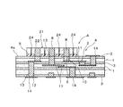
以下、この多層セラミック電子部品の製造方法について、図2〜4の各断面図を参照しつつ説明する。
図2(a)は本願発明の実施例1にかかる多層セラミック電子部品の製造方法の一工程において形成された、焼成に付される前の積層体の構造を示す断面図、図2(b)は要部を拡大して示す断面図である。
Hereinafter, a method for manufacturing the multilayer ceramic electronic component will be described with reference to the cross-sectional views of FIGS.
FIG. 2A is a cross-sectional view showing the structure of a laminate formed in one step of the method for manufacturing a multilayer ceramic electronic component according to Example 1 of the present invention before being fired, and FIG. FIG. 2 is an enlarged cross-sectional view showing a main part.
(1)まず、図2(a),(b)に示す積層体Aを作製する。この積層体Aを作製するにあたって、未焼結セラミック基材層1と、未焼結セラミック基材層1の平面方向の収縮を抑制するための収縮抑制層3とを積層した、未焼結導体パターン2を備えた未焼結多層セラミック素体4の第1主面4aに、未焼結セラミック基材層1の焼成温度において消失する消失層5を介して、未焼結突起状電極8を有する補助層21を、未焼結多層セラミック素体4の未焼結導体パターン2の一部である未焼結接続電極2aと未焼結突起状電極8の下側端面6とが当接するような態様で配置する。これにより、図2(a),(b)に示すような構造を有する積層体Aが形成される。
(1) First, a laminate A shown in FIGS. 2A and 2B is manufactured. In producing this laminate A, a non-sintered conductor obtained by laminating a non-sintered
なお、未焼結導体パターン2は、面内導体用の導電性ペースト11、未焼結セラミック基材層1および収縮抑制層3に形成された貫通孔12に充填されたビアホール導体用の導電性ペースト13、未焼結多層セラミック素体1の表面に配設された外部導体用の導電性ペースト14などから形成されている。
また、異なる層に配設された所定の面内導体用の導体ペースト11どうし、あるいは所定の面内導体用の導体ペースト11と外部導体用の導体ペースト14は、ビアホール導体用の導体ペースト13を介して、互いに接続されている。
The
In addition, the conductor pastes 11 for predetermined in-plane conductors disposed in different layers, or the
上述の積層体Aを形成する場合、具体的には、まず、未焼結セラミック基材層1および収縮抑制層3を構成することになるセラミックグリーンシートを用意し、このセラミックグリーンシートに、適宜、面内導体、ビアホール導体、および外部導体を形成するための導電性ペースト11,13,14を付与する。
そして、収縮抑制層3が未焼結多層セラミック素体4の上下の両主面に配置され、かつ、未焼結多層セラミック素体4を構成する未焼結セラミック基材層1間に配置されるように、上記セラミックグリーンシートを、所定の順序および方向で積層、圧着し、図2(a),(b)に示すような未焼結多層セラミック素体(セラミックグリーンシート成形体)4を得る。
When forming the above-described laminate A, specifically, first, a ceramic green sheet that will form the unsintered ceramic
And the shrinkage |
なお、この実施例1では、未焼結セラミック基材層1として、Ba−Al−Si−O系セラミック材を用い、収縮抑制層3として、アルミナを主成分とするセラミックグリーンシートを用いた。
そして、予め用意しておいた、一方主面に消失層5が配設された、未焼結セラミック基材層1を構成するセラミックの焼結温度では実質的に焼結しないセラミック粉末を主成分とする補助層21に、補助層21と消失層5の両方を貫通する突起状電極形成用貫通孔22を形成し、突起状電極形成用貫通孔22内に突起状電極形成用の導電性ペースト(未焼結突起状電極8)を充填する。なお、この実施例1では、一方主面に消失層5が配設された補助層21として、上述の収縮抑制層3を、樹脂などの焼成工程で消失するようなキャリアフィルム(消失層)上に成形したものを用いている。
また、収縮抑制層3がガラス成分を含むものである場合には、収縮抑制層3を構成する材料からガラス成分を除去した材料からなる層を補助層21として用いることも可能である。
In Example 1, a Ba—Al—Si—O-based ceramic material was used as the unsintered
The main component is ceramic powder that is prepared in advance and that does not substantially sinter at the sintering temperature of the ceramic constituting the unsintered ceramic
When the
なお、消失層5として機能するキャリアフィルムとしては、ポリプロピレンからなるシートを使用している。
それから、貫通孔22に突起状電極形成用の導電性ペーストを充填した補助層21を、未焼結多層セラミック素体(セラミックグリーンシート成形体)4の所定位置に、消失層5が、未焼結多層セラミック素体4側となるように積層、圧着する。これにより、図2(a),(b)に示すような構造を有する積層体Aが得られる。
In addition, as a carrier film which functions as the vanishing
Then, the
なお、このとき、補助層21を、例えば、別のキャリアフィルム上などに予め整列させておき、キャリアフィルム上に保持された状態で位置合わせを行うことにより、効率よく、未焼結多層セラミック素体4の第1主面4aの所定位置に補助層21を配置することができる。
なお、未焼結セラミック基材層1、収縮抑制層3、消失層5、および、補助層21を積層する際の積層順序や、積層方法などは、最終的に図2(a)に示されているような構造を有する積層体Aを得ることができればよく、特に前述した方法に限定されるものではない。
At this time, the
In addition, the lamination order, lamination method, etc. at the time of laminating | stacking the unsintered ceramic
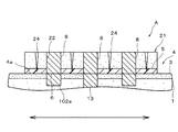
(2)それから、この積層体Aを、未焼結セラミック基材層1および未焼結突起状電極8が焼結する温度で焼成することにより、図3(a),(b)に示すように、消失層5(図2(a),(b))を消失させるとともに、未焼結セラミック基材層1および未焼結突起状電極8を焼結させる。なお、図3(a),(b)において、図1および図2(a),(b)と同一符号を付した部分は、同一または相当する部分を示す。
(2) Then, the laminate A is fired at a temperature at which the unsintered
この焼成工程で、未焼結セラミック基材層1から拡散するガラス成分により、収縮抑制層3中の難焼結性セラミック粉体が固着され、その結果、収縮抑制層3が、セラミック基材層101と固着一体化する。
また、焼結後の突起状電極108は、後述する挙動によって底面である多層セラミック素体側の下側端面106の面積が、底面106と対向する上側端面107の面積より大きい、台形状となる。
In this firing step, the hardly sinterable ceramic powder in the
In addition, the sintered protruding
これにより、セラミック基材層101と、収縮抑制層103とを備え、所定の導体パターン102を備えた多層セラミック素体104と、多層セラミック素体104の第1主面104aに、導体パターン102の一部を構成する接続電極102aと接続するように配設された、台形状の突起状電極108と、補助層21とを備えた積層体A1が得られる。
As a result, the multilayer
なお、この焼成工程において、積層体A1は、セラミック基材層101を構成するセラミック材料が焼結し、かつ、収縮抑制層103を構成する材料が焼結しない温度で焼成される。これにより、セラミック基材層101が収縮しようとする際に、収縮抑制層103が、セラミック基材層101の収縮を抑制するように作用する。これにより、寸法精度の高い、突起状電極付きの多層セラミック素体104を作製することができる。
なお、焼成工程における雰囲気は、セラミック基材層101を構成するセラミック材料の種類や未焼結導体パターン2を形成するための導電性ペーストに含まれる導電性粉末の種類などに応じて、適宜調整される。
In this firing step, the laminate A1 is fired at a temperature at which the ceramic material constituting the
The atmosphere in the firing step is appropriately adjusted according to the type of ceramic material constituting the ceramic
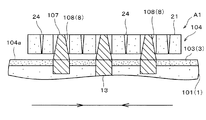
(3)次に、図4(a),(b)に示すように、消失層が消失した状態の積層体から、実質的に焼結していない補助層(セラミック補助層)21を除去して、焼結した突起状電極108を、焼結した多層セラミック素体104の第1主面104aに露出させる。なお、図4(a),(b)において、図1および図3(a),(b)と同一符号を付した部分は、同一または相当する部分を示す。
なお、補助層21は実質的に焼結していないので、その除去は、焼結後の多層セラミック素体104を軽く振ったり、弱いエアーブローを行ったりすることにより容易に行うことができる。
(3) Next, as shown in FIGS. 4A and 4B, the auxiliary layer (ceramic auxiliary layer) 21 that is not substantially sintered is removed from the laminated body in which the vanishing layer has disappeared. Thus, the sintered protruding
Since the
(4)それから、突起状電極108の上側端面107に、はんだ109を介して、表面実装型電子部品(この実施例1では半導体素子)110を実装する(図1参照)。
なお、突起状電極108の上側端面107上への表面実装型電子部品110の実装は、例えば、突起状電極108の上側端面107にクリームはんだを供給し、その上に表面実装型電子部品110を載置してリフローする方法などにより行うことができる。
これにより、図1に示すような構造を有する突起状電極付き多層セラミック電子部品が得られる。
(4) Then, a surface mount type electronic component (a semiconductor element in this embodiment 1) 110 is mounted on the
For example, the surface-mounted
Thereby, a multilayer ceramic electronic component with protruding electrodes having a structure as shown in FIG. 1 is obtained.
上述のようにして製造される突起状電極付き多層セラミック電子部品の構成について、以下にさらに詳しく説明する。 The structure of the multilayer ceramic electronic component with protruding electrodes manufactured as described above will be described in more detail below.
セラミック基材層101は、セラミック材料が焼結されてなり、多層セラミック電子部品の基板特性を支配する。
セラミック基材層101の厚みは、焼成後に10μm〜100μmとすることが好ましい。セラミック基材層101の焼成後の厚みは、必ずしも、この範囲内に限定されるものではないが、後述する焼結可能な厚みの収縮抑制層103によって収縮を抑制することが可能な最大厚み以下に抑えることが好ましい。なお、セラミック基材層101の厚みは、必ずしも各層が同じである必要はない。
The ceramic
The thickness of the
また、セラミック基材層101を構成するセラミック材料としては、焼成中にその一部(例えば、ガラス成分)が、収縮抑制層103に浸透するものを用いることが望ましい。
また、セラミック基材層101を構成するセラミック材料としては、銀や銅などの低融点金属からなる導体と同時焼成することができるように、比較的低温、例えば1050℃以下で焼成可能なLTCC(低温焼成セラミック;Low Temperature Co−fired Ceramic)を用いることが好ましい。具体的には、アルミナとホウケイ酸系ガラスとを混合したガラスセラミックや、上述のように、焼成中にガラス成分を生成するBa−Al−Si−O系セラミックなどを用いることができる。なお、上記実施例1では、セラミック基材層101を構成するセラミック材料として、焼成中にガラス成分を生成するBa−Al−Si−O系セラミックを用いている。
Moreover, as a ceramic material which comprises the ceramic
Moreover, as a ceramic material which comprises the ceramic
収縮抑制層103を構成する材料としては、特にセラミック基材層101にLTCCを用いている場合、アルミナ、ジルコニア、シリカなどの難焼結性セラミックを用いることが望ましい。この実施例1では上述のように収縮抑制層103を構成する材料としてアルミナを用いている。
また、収縮抑制層103は、セラミック基材層101から浸透してきた、セラミック基材層101を構成するセラミック材料の一部(例えばガラス)により固着され、これにより、収縮抑制層103が固化するとともに、セラミック基材層101と収縮抑制層103の接合がもたらされる。収縮抑制層中にあらかじめ焼成時に収縮抑制層を焼結させない程度のガラスが含まれていてもよい。
As a material constituting the
Further, the
収縮抑制層103は、セラミック基材層101を構成するセラミック材料よりも高い焼結温度を有する材料を含有しているため、焼成過程での、セラミック基材層101の平面方向への収縮を抑制する機能を発揮する。また前述したように、収縮抑制層103は、セラミック基材層101を構成するセラミック材料の一部が浸透することによって固着、接合される。そのため、厳密にはセラミック基材層101および収縮抑制層103の状態や所望の収縮抑制効果(拘束力)、焼成条件などにも依存するが、収縮抑制層103の厚みは、概ね焼成後に1μm〜5μmであることが好ましい。
この実施例1では、セラミック基材層101の厚みは、焼成後に50μmとなるように設定し、収縮抑制層103の厚みは、焼成後に5μmとなるように設定した。
Since the
In Example 1, the thickness of the ceramic
また前述の、面内導体111,ビアホール112に充填されたビアホール導体113、外部導体114を形成するための材料としては、セラミック基材層101と同時焼成が可能な導電性成分を主成分とするものであれば、広く公知のものを使用することが可能である。具体的には、Cu、Ag、Ni、Pd、およびそれらの酸化物、合金成分などを使用することが可能である。
なお、この実施例1では、Cuを主成分とした導電性ペーストを用いて、上述の各導体部を形成した。
The material for forming the in-
In Example 1, each conductor portion described above was formed using a conductive paste containing Cu as a main component.
また、補助層21としては、上記の収縮抑制層103と同じ材料、すなわち、アルミナ、ジルコニア、シリカなどからなるセラミックグリーンシートを用いることができる。
As the
また、消失層5としては、焼成工程で分解、消失するものであれば、広く公知の材料からなるものを用いることが可能である。具体的には、ポリプロピレン、ポリエチレン、ポリスチレン、結晶性セルロース、などを有機バインダー中に分散させたものが好ましい例として挙げられる。
Moreover, as the vanishing
[特性の評価]
上記実施例1の方法で作製した多層セラミック電子部品について、特性を評価した。
なお、比較のため、以下の比較例1,比較例2および比較例3の各試料を作製し、上記実施例1の多層セラミック電子部品とともに、特性の評価に供した。
[Characteristic evaluation]
The characteristics of the multilayer ceramic electronic component produced by the method of Example 1 were evaluated.
For comparison, the following samples of Comparative Example 1, Comparative Example 2, and Comparative Example 3 were prepared and used for evaluation of characteristics together with the multilayer ceramic electronic component of Example 1 described above.
[比較例1]
消失層を配設せずに製造したことを除いては、上記実施例1の場合と同様の方法で製造した突起状電極付き多層セラミック電子部品。
[比較例2]
多層セラミック素体が収縮抑制層を備えていないことを除いては、上記実施例1の多層セラミック電子部品と同様の方法で製造された突起状電極付き多層セラミック電子部品。
[比較例3]
消失層を配設せずに製造され、かつ、多層セラミック素体が収縮抑制層を備えていないことを除いては、上記実施例1の多層セラミック電子部品と同様の構成を有する多層セラミック電子部品。
[Comparative Example 1]
A multilayer ceramic electronic component with protruding electrodes manufactured by the same method as in Example 1 except that it was manufactured without disposing the vanishing layer.
[Comparative Example 2]
A multilayer ceramic electronic component with protruding electrodes manufactured by the same method as that of the multilayer ceramic electronic component of Example 1 except that the multilayer ceramic body does not include a shrinkage suppression layer.
[Comparative Example 3]
A multilayer ceramic electronic component having the same configuration as that of the multilayer ceramic electronic component of Example 1 except that the multilayer ceramic body is not provided with a shrinkage suppression layer, and is manufactured without providing the vanishing layer. .
上記実施例1の多層セラミック電子部品および、比較例1,2,3の多層セラミック電子部品について、外観検査を行い、補助層除去の容易性、突起状電極の脱落の発生率、突起状電極の位置ずれの発生の有無を調べるとともに、突起状電極の導通率を調べた。
その結果を表1に示す。
Appearance inspection was performed on the multilayer ceramic electronic component of Example 1 and the multilayer ceramic electronic components of Comparative Examples 1, 2, and 3. Ease of removal of the auxiliary layer, the rate of occurrence of the protruding electrode dropout, The occurrence of misalignment was examined and the conductivity of the protruding electrode was examined.
The results are shown in Table 1.

なお、表1において、突起状電極の脱落の発生率は、評価に供した全試料数に対する、突起状電極の脱落が認められた試料の数の割合を示している。
また、突起状電極の導通率は、評価に供した全試料数に対する、突起状電極が導通していることが確認された試料の数の割合を示している。
In Table 1, the occurrence rate of the protruding electrodes is the ratio of the number of the samples in which the protruding electrodes were removed to the total number of samples used for the evaluation.
Further, the conductivity of the protruding electrode indicates the ratio of the number of samples in which the protruding electrode is confirmed to be conductive with respect to the total number of samples subjected to the evaluation.
表1に示すように、比較例1では、消失層を設けることなく製造するようにしたため、補助層の除去が困難で、残留が認められ、突起状電極の脱落の発生率も40%と高かった。ただし、比較例1は収縮抑制層を備えているので、突起状電極の位置ずれの発生は認められず、突起状電極の導通率も100%であった。 As shown in Table 1, in Comparative Example 1, since the manufacturing was performed without providing the vanishing layer, it was difficult to remove the auxiliary layer, the residue was observed, and the incidence rate of the protruding electrode dropout was as high as 40%. It was. However, since Comparative Example 1 includes the shrinkage suppression layer, the occurrence of positional deviation of the protruding electrodes was not recognized, and the conductivity of the protruding electrodes was 100%.
また、比較例2は、消失層を備えているが、収縮抑制層を備えていないため、補助層の除去は容易であったが、多層セラミック素体と突起状電極の間で収縮率の差が生じ、この収縮率の差が生じた部分(滑りが発生した部分)では、後述する挙動によって突起状電極が台形状とならずに、直方体形状となり、突起状電極の脱落および位置ずれが発生し、突起状電極の導通率も75%と低くなることが確認された。また、突起状電極の位置ずれが発生するため、表面実装型電子部品の実装性に劣るという問題点がある。 Further, Comparative Example 2 includes the disappearance layer, but does not include the shrinkage suppression layer, and thus the auxiliary layer can be easily removed. However, there is a difference in shrinkage between the multilayer ceramic body and the protruding electrode. In the part where the difference in shrinkage rate occurs (the part where the slip occurs), the protruding electrode does not become trapezoidal due to the behavior described later, but it becomes a rectangular parallelepiped, and the protruding electrode is dropped and misaligned. In addition, it was confirmed that the conductivity of the protruding electrode was as low as 75%. Further, since the positional deviation of the protruding electrodes occurs, there is a problem that the mountability of the surface mount electronic component is inferior.
また、比較例3は、消失層を設けることなく製造され、しかも、多層セラミック素体が収縮抑制層を備えていないため、補助層の除去は困難で、残留があり、また、多層セラミック素体と突起状電極の間で収縮率の差が生じ、この収縮率の差が生じた部分(滑りが発生した部分)では、突起状電極が台形状とならずに、直方体形状となり、突起状電極の脱落および位置ずれが発生し、突起状電極の導通率も80%と低くなることが確認された。また、突起状電極の位置ずれが発生するため、表面実装型電子部品の実装性に劣るという問題点がある。 Further, Comparative Example 3 was manufactured without providing the vanishing layer, and since the multilayer ceramic body was not provided with a shrinkage suppression layer, it was difficult to remove the auxiliary layer and there was a residue. A difference in contraction rate occurs between the projection electrode and the protruding electrode, and in the portion where the difference in contraction rate occurs (where the slip occurs), the protruding electrode does not have a trapezoidal shape but a rectangular parallelepiped shape. It was confirmed that dropout and misalignment occurred, and the conductivity of the protruding electrode was as low as 80%. Further, since the positional deviation of the protruding electrodes occurs, there is a problem that the mountability of the surface mount electronic component is inferior.
これに対し、実施例1の多層セラミック電子部品の場合、製造工程で、補助層と未焼結多層セラミック素体との間に消失層を設けるようにしているとともに、多層セラミック素体が収縮抑制層を備えているため、補助層の除去の容易性、突起状電極の脱落の発生率、突起状電極の位置ずれの有無、および、突起状電極の導通率、のいずれの特性に関しても、各比較例の多層セラミック電子部品に比べて、良好な特性が得られることが確認された。 On the other hand, in the case of the multilayer ceramic electronic component of Example 1, in the manufacturing process, a vanishing layer is provided between the auxiliary layer and the unsintered multilayer ceramic body, and the multilayer ceramic body suppresses shrinkage. Each of the characteristics of the ease of removal of the auxiliary layer, the rate of occurrence of dropout of the protruding electrode, the presence or absence of misalignment of the protruding electrode, and the conductivity of the protruding electrode. It was confirmed that good characteristics can be obtained as compared with the multilayer ceramic electronic component of the comparative example.
なお、実施例1の多層セラミック電子部品においては、多層セラミック素体の表面に収縮抑制層が配置されているので、突起状電極の下側端面が多層セラミック素体の導体パターンに接続した状態で焼成される。したがって、多層セラミック素体の平面方向への収縮が抑制されるため、突起状電極の下側部分は収縮が抑制され、上側部分は下側部分よりも多く収縮することになり、焼成後の突起状電極は台形状となる。その結果、多層セラミック素体への接合強度が向上するとともに、脱落や位置ずれが発生しにくくなり、導通性信頼性が高く、表面実装型電子部品の実装性に優れた、突起状電極付き多層セラミック電子部品を得ることが可能になる。 In the multilayer ceramic electronic component of Example 1, since the shrinkage suppression layer is disposed on the surface of the multilayer ceramic body, the lower end surface of the protruding electrode is connected to the conductor pattern of the multilayer ceramic body. Baked. Therefore, since the shrinkage of the multilayer ceramic body in the planar direction is suppressed, the lower part of the projecting electrode is restrained from shrinking, and the upper part contracts more than the lower part. The electrode is trapezoidal. As a result, the bonding strength to the multilayer ceramic body is improved, dropout and misalignment are less likely to occur, the continuity reliability is high, and the mountability of surface mount electronic components is excellent. Ceramic electronic components can be obtained.
図5は本願発明の他の実施例(実施例2)にかかる突起状電極付き多層セラミック電子部品の製造工程で作製した、スリットを備えた状態の積層体Aを示す図、図6は図5の積層体Aの要部を拡大して示す図である。なお、図5において、図1および図2(a),(b)と同一符号を付した部分は、同一または相当する部分を示す。 FIG. 5 is a view showing a laminated body A having slits, which is produced in the manufacturing process of the multilayer ceramic electronic component with protruding electrodes according to another embodiment (Example 2) of the present invention, and FIG. It is a figure which expands and shows the principal part of the laminated body A of. In FIG. 5, the parts denoted by the same reference numerals as those in FIGS. 1 and 2 (a) and 2 (b) indicate the same or corresponding parts.
この実施例2においても、まず、実施例1と同様にして、図5に示すように、未焼結導体パターン2を備えた未焼結セラミック基材層1と、未焼結セラミック基材層1の平面方向の収縮を抑制するための収縮抑制層3とが積層された未焼結多層セラミック素体4の第1主面4aに、未焼結セラミック基材層1の焼成温度で消失する消失層5を介して、複数の未焼結突起状電極8を有する補助層21を、未焼結多層セラミック素体4の未焼結導体パターンと未焼結突起状電極8の下側端面6とが当接するような態様で配置することにより、積層体Aを形成した。
Also in this Example 2, first, similarly to Example 1, as shown in FIG. 5, the unsintered
そして、図5および図6に示すように、補助層21の、各未焼結突起状電極8の間の位置に、補助層21の上側主面から下側主面に至るスリット(分割溝)24を形成した。なお、この実施例2では、スリット24を、補助層21の上側主面から、補助層21の下面側に配設された消失層5の厚み方向の途中にまで達するように形成した。
Then, as shown in FIGS. 5 and 6, slits (dividing grooves) extending from the upper main surface to the lower main surface of the
それから、上述のようにして、補助層21にスリット24が形成された積層体Aを、上記実施例1の場合と同様にして焼成した。これにより、図7に示すように、消失層5が消失し、補助層21は実質的に未焼結で、かつ、補助層21の、焼結した各突起状電極108の間の位置にスリット24が形成された状態の、焼結済みの積層体A1が得られる。
次に、焼結済みの積層体A1から、スリット24が形成された、実質的に未焼結の補助層21を除去する。
Then, as described above, the laminate A in which the
Next, the substantially unsintered
なお、補助層21にスリット24が形成されていることから、積層体A1を軽く振ったり、弱いエアーブローを行ったりすることにより、極めて容易に補助層21の除去を行うことができる。
それから、突起状電極108の上側端面107に、はんだ109を介して、表面実装型電子部品110を実装することにより、図1に示すような構造を有する多層セラミック電子部品を得ることができる。
In addition, since the
Then, by mounting the surface-mounted
[特性の評価]
実施例2の方法で作製した多層セラミック電子部品についても上記実施例1の場合と同様の方法で特性を評価し、上記実施例1の方法で作製した多層セラミック電子部品と比較した。
その結果を表2に示す。
[Characteristic evaluation]
The characteristics of the multilayer ceramic electronic component produced by the method of Example 2 were also evaluated in the same manner as in Example 1 above, and compared with the multilayer ceramic electronic component produced by the method of Example 1.
The results are shown in Table 2.
なお、表2に示した、多層セラミック電子部品の特性の概念および評価方法は、上記実施例1の場合と同様である。
表2に示すように、この実施例2の製造方法によれば、補助層21にスリット24を形成するようにしていることから、補助層21が、突起状電極8毎に小片化されるため、焼成後の補助層21の除去が一層容易になることが確認された。
Note that the concept and evaluation method of the characteristics of the multilayer ceramic electronic component shown in Table 2 are the same as those in Example 1.
As shown in Table 2, according to the manufacturing method of Example 2, since the
すなわち、上記実施例1の方法の場合には、突起状電極8が配置されている領域一帯の補助層21を一括して除去する必要があったが、実施例2では、各突起状電極8毎に、小片化された補助層21を除去すればよいため、補助層21を除去する工程で突起状電極8に加わる応力を減少させることが可能となり、結果として、突起状電極8の脱落が生じることを回避することが可能になる。
That is, in the case of the method of the first embodiment, it is necessary to remove the
なお、この実施例2では、スリット24を、補助層21の下側に配設された消失層5に達するように形成しているが、スリット24は、少なくとも補助層の上面側から下面側にまで達していればよく、消失層5にまで入り込んでいなくてもよい。
また、スリット24の深さを、補助層21の厚み方向の途中までとした場合にも、具体的な条件によっては、十分に補助層の除去性を向上させることができる場合がある。
In Example 2, the
Further, even when the depth of the
なお、上記実施例1および2では、補助層および消失層を多層セラミック素体の第1主面の一部領域に形成するようにしているが、補助層および消失層を多層セラミック素体の第1主面の全体に形成するように構成することも可能である。 In Examples 1 and 2, the auxiliary layer and the disappearing layer are formed in a partial region of the first main surface of the multilayer ceramic body. However, the auxiliary layer and the disappearing layer are formed in the first layer of the multilayer ceramic body. It is also possible to configure so as to be formed on the entire surface of one main surface.
また、上記実施例1および2では、多層セラミック素体の内部にも収縮抑制層を配置しているが、内部への収縮抑制層の配設量(枚数)が少ない場合、焼成工程で多層セラミック素体に平面方向への収縮が生じることになり、実施例1のように、補助層にスリットが形成されていない場合は、補助層に配設された突起状電極と多層セラミック素体の間で位置ずれが生じやすくなるが、実施例2では、補助層にスリットを形成するようにしているので、補助層による平面方向への収縮抑制力を解消することが可能になり、結果として、突起状電極と多層セラミック素体の間の位置ずれ(具体的には、多層セラミック素体の接続電極と、突起状電極との間の位置ずれ)の発生を抑制することが可能になる。 Further, in Examples 1 and 2 described above, the shrinkage suppression layer is also disposed inside the multilayer ceramic body. However, when the amount (number of sheets) of the shrinkage suppression layer disposed in the interior is small, the multilayer ceramic is subjected to a firing process. When the element body is contracted in the plane direction and no slit is formed in the auxiliary layer as in the first embodiment, the gap between the protruding electrode disposed in the auxiliary layer and the multilayer ceramic element body is reduced. However, in Example 2, since the slit is formed in the auxiliary layer, it is possible to eliminate the shrinkage suppression force in the plane direction by the auxiliary layer. It is possible to suppress the occurrence of misalignment between the electrode and the multilayer ceramic element (specifically, misalignment between the connection electrode of the multilayer ceramic element and the protruding electrode).
すなわち、実施例2のように、補助層にスリットを形成することによって多層セラミック素体側の収縮抑制層の配設条件を大幅に緩和することが可能となり、よりフレキシブルな回路設計を可能にすることができるようになる。 That is, as in Example 2, it is possible to significantly relax the conditions for disposing the shrinkage suppression layer on the multilayer ceramic body side by forming a slit in the auxiliary layer, and to enable more flexible circuit design. Will be able to.
なお、上記実施例1および2では、補助層を、多層セラミック素体を構成するセラミックの焼成温度では実質的に焼結しない材料から構成するようにしている(具体的には収縮抑制層を構成する材料と同じ材料を用いている)が、補助層の構成材料はこれに限られるものではなく、他の材料からなる補助層、例えば、樹脂材料からなる補助層を用いることも可能である。 In Examples 1 and 2, the auxiliary layer is made of a material that does not substantially sinter at the firing temperature of the ceramic constituting the multilayer ceramic body (specifically, the shrinkage suppression layer is formed). However, the constituent material of the auxiliary layer is not limited to this, and an auxiliary layer made of another material, for example, an auxiliary layer made of a resin material can be used.
本願発明は、さらにその他の点においても上記実施例に限定されるものではなく、焼成工程の前の段階で形成される上記積層体の具体的な構成、積層体の形成方法、多層セラミック素体を構成するセラミック基材層および収縮抑制層の積層態様、積層体の焼成条件や焼成方法、突起状電極上に搭載される表面実装型電子部品の種類などに関し、発明の範囲内において、種々の応用、変形を加えることが可能である。 The invention of the present application is not limited to the above embodiment in other points as well, and the specific structure of the laminate, the method of forming the laminate, the multilayer ceramic body formed in the stage before the firing step Within the scope of the invention, there are various types of laminates of the ceramic base material layer and the shrinkage suppression layer, the firing conditions and firing method of the laminate, the types of surface-mounted electronic components mounted on the protruding electrodes, etc. Applications and modifications can be added.
本願発明によれば、表面に突起状電極を備えた多層セラミック電子部品を、複雑な製造工程を必要とせずに、突起状電極の位置ずれを生じることなく、効率よく製造することが可能になる。
したがって、本願発明は、例えば、VLSI、ULSIなどの半導体デバイスが実装されるマルチチップモジュール(MCM)などの用途に用いるのに適した突起状電極付き多層セラミック電子部品、および、その製造方法に関する分野に広く利用することができる。
According to the present invention, a multilayer ceramic electronic component having a protruding electrode on its surface can be efficiently manufactured without requiring a complicated manufacturing process and without causing a positional shift of the protruding electrode. .
Accordingly, the present invention relates to a multilayer ceramic electronic component with protruding electrodes suitable for use in applications such as a multichip module (MCM) on which semiconductor devices such as VLSI and ULSI are mounted, and a method for manufacturing the same. Can be widely used.
A 積層体
A1 焼成後の積層体
1 未焼結セラミック基材層
2 未焼結導体パターン
2a 未焼結接続電極
3 焼成前の収縮抑制層
4 未焼結多層セラミック素体
4a 未焼結多層セラミック素体の第1主面
5 消失層
6 未焼結突起状電極の下側端面
8 未焼結突起状電極
11 面内導体用の導電性ペースト
12 貫通孔
13 ビアホール導体用の導電性ペースト
14 外部導体用の導電性ペースト
21 補助層
22 補助層の突起状電極形成用の貫通孔
24 スリット
101 セラミック基材層
102 導体パターン
102a 接続電極
103 焼成後の収縮抑制層
104 多層セラミック素体
104a 多層セラミック素体の第1主面
106 突起状電極の下側端面(底面)
107 突起状電極の上側端面(上面)
108 突起状電極
109 はんだ
110 表面実装型電子部品
111 面内導体
112 ビアホール
113 ビアホール導体
114 外部導体(表面導体)
A laminate A1 laminate after firing 1 unsintered
107 Upper end surface (upper surface) of protruding electrode
108
Claims (10)
前記積層体を、前記未焼結セラミック基材層および前記未焼結突起状電極が焼結する温度で焼成することにより、前記消失層の少なくとも主要部を消失させるとともに、前記未焼結セラミック基材層および前記未焼結突起状電極を焼結させる工程と
を具備することを特徴とする突起状電極付き多層セラミック電子部品の製造方法。 A non-sintered multilayer ceramic body comprising a non-sintered ceramic base material layer and a non-sintered ceramic base material layer having a non-sintered conductor pattern, wherein a non-sintered ceramic base material layer and a shrinkage suppression layer for suppressing shrinkage in a planar direction are laminated. An auxiliary layer having unsintered protruding electrodes is formed on the first main surface of the unsintered multilayer ceramic element through a disappearing layer in which at least a main part disappears at the firing temperature of the unsintered ceramic base layer. Forming a laminated body arranged in such a manner that the unsintered conductor pattern of the body and the unsintered protruding electrode are in contact with each other;
The laminate is fired at a temperature at which the unsintered ceramic base layer and the unsintered protruding electrode sinter, thereby eliminating at least the main part of the disappearing layer and the unsintered ceramic base. And a step of sintering the unsintered projecting electrode. A method for producing a multilayer ceramic electronic component with a projecting electrode.
Priority Applications (1)
| Application Number | Priority Date | Filing Date | Title |
|---|---|---|---|
| JP2006160283A JP4826348B2 (en) | 2006-06-08 | 2006-06-08 | Method for producing multilayer ceramic electronic component with protruding electrodes |
Applications Claiming Priority (1)
| Application Number | Priority Date | Filing Date | Title |
|---|---|---|---|
| JP2006160283A JP4826348B2 (en) | 2006-06-08 | 2006-06-08 | Method for producing multilayer ceramic electronic component with protruding electrodes |
Publications (2)
| Publication Number | Publication Date |
|---|---|
| JP2007329355A JP2007329355A (en) | 2007-12-20 |
| JP4826348B2 true JP4826348B2 (en) | 2011-11-30 |
Family
ID=38929615
Family Applications (1)
| Application Number | Title | Priority Date | Filing Date |
|---|---|---|---|
| JP2006160283A Expired - Fee Related JP4826348B2 (en) | 2006-06-08 | 2006-06-08 | Method for producing multilayer ceramic electronic component with protruding electrodes |
Country Status (1)
| Country | Link |
|---|---|
| JP (1) | JP4826348B2 (en) |
Families Citing this family (2)
| Publication number | Priority date | Publication date | Assignee | Title |
|---|---|---|---|---|
| WO2009087839A1 (en) * | 2008-01-11 | 2009-07-16 | Murata Manufacturing Co., Ltd. | Method for manufacturing ceramic electronic component and ceramic electronic component |
| CN113579363B (en) * | 2021-09-01 | 2022-05-03 | 福建省闽铝轻量化汽车制造有限公司 | Method and system for processing multilayer web |
Family Cites Families (4)
| Publication number | Priority date | Publication date | Assignee | Title |
|---|---|---|---|---|
| JP2681327B2 (en) * | 1992-07-28 | 1997-11-26 | 株式会社住友金属エレクトロデバイス | Method for manufacturing bumped circuit board |
| JP3656484B2 (en) * | 1999-03-03 | 2005-06-08 | 株式会社村田製作所 | Manufacturing method of ceramic multilayer substrate |
| JP2001085470A (en) * | 1999-09-16 | 2001-03-30 | Fujitsu Ltd | Semiconductor device and manufacturing method therefor |
| JP3582513B2 (en) * | 2001-11-14 | 2004-10-27 | セイコーエプソン株式会社 | Semiconductor device and its manufacturing method, circuit board, and electronic equipment |
-
2006
- 2006-06-08 JP JP2006160283A patent/JP4826348B2/en not_active Expired - Fee Related
Also Published As
| Publication number | Publication date |
|---|---|
| JP2007329355A (en) | 2007-12-20 |
Similar Documents
| Publication | Publication Date | Title |
|---|---|---|
| JP4254860B2 (en) | Multilayer substrate with built-in chip-type electronic component and method for manufacturing the same | |
| JP3982563B2 (en) | Ceramic electronic component and method for manufacturing the same | |
| JP4858538B2 (en) | Multilayer ceramic electronic component, multilayer ceramic substrate, and method of manufacturing multilayer ceramic electronic component | |
| JPWO2007049458A1 (en) | Multilayer electronic component, electronic device, and method of manufacturing multilayer electronic component | |
| JP2008021883A (en) | Multilayer ceramic electronic component, manufacturing method therefor, and multilayer ceramic substrate | |
| JP2008004733A (en) | Manufacturing method of ceramic substrate | |
| WO2018042846A1 (en) | Electronic device and multilayer ceramic substrate | |
| JP4497247B2 (en) | Manufacturing method of multilayer ceramic electronic component | |
| JP2007273914A (en) | Wiring board and method of manufacturing same | |
| JP4826348B2 (en) | Method for producing multilayer ceramic electronic component with protruding electrodes | |
| WO2009119198A1 (en) | Process for producing ceramic substrate | |
| JP6128209B2 (en) | MULTILAYER WIRING BOARD, MANUFACTURING METHOD THEREOF, AND PROBE CARD BOARD | |
| JP4826253B2 (en) | Method for manufacturing ceramic multilayer substrate and ceramic multilayer substrate | |
| JP2001339166A (en) | Multilayer wiring board and method of production | |
| JP2006216709A (en) | Multilayered wiring board with built-in multilayered electronic component, and multilayered electronic component | |
| JP4900227B2 (en) | Multilayer ceramic substrate manufacturing method, multilayer ceramic substrate, and electronic component using the same | |
| JP4535801B2 (en) | Ceramic wiring board | |
| JP2002050869A (en) | Method of manufacturing multilayered wiring board | |
| JP2007095862A (en) | Multilayer ceramic assembled substrate manufacturing method thereof, multilayer and multilayer ceramic substrate | |
| JP2004165343A (en) | Laminated ceramic electronic component and its manufacturing method | |
| JP3879276B2 (en) | Manufacturing method of ceramic multilayer substrate | |
| JP3188086B2 (en) | Ceramic wiring board, its manufacturing method and its mounting structure | |
| JP2006032442A (en) | Multi-layer substrate and manufacturing method therefor | |
| JP2011029534A (en) | Multilayer wiring board | |
| JP4645962B2 (en) | Multilayer ceramic substrate |
Legal Events
| Date | Code | Title | Description |
|---|---|---|---|
| A621 | Written request for application examination |
Free format text: JAPANESE INTERMEDIATE CODE: A621 Effective date: 20081015 |
|
| A977 | Report on retrieval |
Free format text: JAPANESE INTERMEDIATE CODE: A971007 Effective date: 20110203 |
|
| A131 | Notification of reasons for refusal |
Free format text: JAPANESE INTERMEDIATE CODE: A131 Effective date: 20110215 |
|
| A521 | Request for written amendment filed |
Free format text: JAPANESE INTERMEDIATE CODE: A523 Effective date: 20110418 |
|
| TRDD | Decision of grant or rejection written | ||
| A01 | Written decision to grant a patent or to grant a registration (utility model) |
Free format text: JAPANESE INTERMEDIATE CODE: A01 Effective date: 20110816 |
|
| A01 | Written decision to grant a patent or to grant a registration (utility model) |
Free format text: JAPANESE INTERMEDIATE CODE: A01 |
|
| A61 | First payment of annual fees (during grant procedure) |
Free format text: JAPANESE INTERMEDIATE CODE: A61 Effective date: 20110829 |
|
| FPAY | Renewal fee payment (event date is renewal date of database) |
Free format text: PAYMENT UNTIL: 20140922 Year of fee payment: 3 |
|
| R150 | Certificate of patent or registration of utility model |
Ref document number: 4826348 Country of ref document: JP Free format text: JAPANESE INTERMEDIATE CODE: R150 Free format text: JAPANESE INTERMEDIATE CODE: R150 |
|
| LAPS | Cancellation because of no payment of annual fees |