JP4818738B2 - LED driving device - Google Patents
LED driving device Download PDFInfo
- Publication number
- JP4818738B2 JP4818738B2 JP2006012603A JP2006012603A JP4818738B2 JP 4818738 B2 JP4818738 B2 JP 4818738B2 JP 2006012603 A JP2006012603 A JP 2006012603A JP 2006012603 A JP2006012603 A JP 2006012603A JP 4818738 B2 JP4818738 B2 JP 4818738B2
- Authority
- JP
- Japan
- Prior art keywords
- voltage
- emitting diode
- light emitting
- circuit
- switching element
- Prior art date
- Legal status (The legal status is an assumption and is not a legal conclusion. Google has not performed a legal analysis and makes no representation as to the accuracy of the status listed.)
- Expired - Fee Related
Links
Images


Classifications
-
- H—ELECTRICITY
- H05—ELECTRIC TECHNIQUES NOT OTHERWISE PROVIDED FOR
- H05B—ELECTRIC HEATING; ELECTRIC LIGHT SOURCES NOT OTHERWISE PROVIDED FOR; CIRCUIT ARRANGEMENTS FOR ELECTRIC LIGHT SOURCES, IN GENERAL
- H05B45/00—Circuit arrangements for operating light-emitting diodes [LED]
- H05B45/30—Driver circuits
- H05B45/37—Converter circuits
- H05B45/3725—Switched mode power supply [SMPS]
Landscapes
- Led Devices (AREA)
Description
本発明は、発光ダイオード(LED)駆動装置に関する。特にLED照明装置に関する。 The present invention relates to a light emitting diode (LED) driving device. In particular, the present invention relates to an LED lighting device.
近年、発光ダイオードを駆動するための発光ダイオード駆動装置が開発され、実用化されている。図13を用いて、特許文献1の従来の発光ダイオード駆動回路について説明する。従来の発光ダイオード駆動回路は、発光ダイオード102と、発光ダイオード102に直列接続されたコイル103と、発光ダイオード102とコイル103に対して並列に接続されたダイオード104を有する。ダイオード104は、コイル103に生じた逆起電力を発光ダイオード102に供給するために設けられる。
In recent years, a light emitting diode driving apparatus for driving a light emitting diode has been developed and put into practical use. A conventional light-emitting diode driving circuit of
さらに、発光ダイオード102、コイル103、およびダイオード104にパルス電圧を印加する直流電源101が設けられる。発光ダイオード102と直流電源101との間には、直流電源101の出力電圧の印加/非印加を切り替えるスイッチング素子105が接続される。スイッチング素子105は、例えばスイッチング・トランジスタと発振器で構成される。また、ダイオード104は、逆バイアスが印加されるように、カソード側が直流電源101の正極側に接続される。
Further, a direct
従来の発光ダイオード駆動回路は、スイッチング素子105がオンのときに、直流電源101の出力電圧を発光ダイオード102に印加して、発光ダイオード102を発光させ、スイッチング素子105がオフのとき、コイル103の逆起電力を利用して、発光ダイオード102を発光させる。
上記のように構成された従来の発光ダイオード駆動装置には、以下の問題がある。発光ダイオード102は容量性の負荷である。また市販されている発光ダイオードは、静電気による破壊を防ぐために、発光素子にコンデンサやツェナーダイオードが静電保護素子として並列接続されていることが多い。そのため、スイッチング素子105がオンして電流遮断期間から電流流通期間に移行し、コイル103の低電位側端子P2の電位変動が大きくなったときに、発光ダイオード102の寄生容量や、静電保護素子として並列接続されているコンデンサやツェナーダイオードの寄生容量に、瞬間的に大きな電流が流れる。このため、瞬時的に発光ダイオード102の順方向電圧が低くなる。発光ダイオード102の両端電圧が変動することにより、発光ダイオードはノイズ発生源となる。この現象は、スイッチング素子105がオンする度に発生するため、直流電源101に伝達される雑音端子電圧が増大する。また、発光ダイオード102の順方向電圧が低くなると、寄生容量に電流が流れ、発光ダイオード102に流れる電流が小さくなり、十分な発光輝度が得られない。
The conventional light emitting diode driving device configured as described above has the following problems. The
本発明は、上記問題に鑑み、簡易な構成で雑音端子電圧を低減できる発光ダイオード駆動装置を提供する。 In view of the above problems, the present invention provides a light emitting diode driving device capable of reducing a noise terminal voltage with a simple configuration.
本発明は、少なくとも1つの発光ダイオードと、チョークコイルと、前記発光ダイオードへの電流の印加/非印加を切り換えるスイッチング素子と前記スイッチング素子のオン/オフのタイミングを制御して前記発光ダイオードに流れる電流を制御する制御回路ブロックとを備えたスイッチング駆動回路と、を有し、前記発光ダイオードと前記スイッチング駆動回路との間に前記チョークコイルを接続することを特徴とする発光ダイオード駆動装置である。 The present invention relates to at least one light emitting diode, a choke coil, a switching element for switching application / non-application of current to the light emitting diode, and a current flowing through the light emitting diode by controlling on / off timing of the switching element. And a control circuit block that controls the switching drive circuit, wherein the choke coil is connected between the light emitting diode and the switching drive circuit.
上記の発光ダイオード駆動装置は、チョークコイルに発生する逆起電力を発光ダイオードに供給する整流ダイオードを更に有する。 The light emitting diode driving device further includes a rectifier diode that supplies a counter electromotive force generated in the choke coil to the light emitting diode.
上記のように構成された本発明の発光ダイオード駆動装置によれば、スイッチング素子がオンして電流遮断期間から電流流通期間に移行したときの、チョークコイルと発光ダイオードとの接続点の電位変動は小さい。そのため、発光ダイオードの寄生容量に電流が流れない。また、発光ダイオードの発光素子に、静電保護素子としてコンデンサやツェナーダイオードが並列接続されている場合であっても、コンデンサやツェナーダイオードの寄生容量にも電流が流れない。発光ダイオードの両端電圧は安定し、発光ダイオードの順方向電圧が瞬時的に低下することは無くなる。その結果、発光ダイオードから発生するノイズが減少し、電圧源に伝達される雑音端子電圧を低減できる。さらに、発光ダイオードの寄生容量に流れる電流を大幅に減少できることにより、電力変換効率の高い発光ダイオード駆動装置を実現できる。 According to the light emitting diode driving device of the present invention configured as described above, the potential fluctuation at the connection point between the choke coil and the light emitting diode when the switching element is turned on and transitions from the current cutoff period to the current distribution period is as follows. small. Therefore, no current flows through the parasitic capacitance of the light emitting diode. In addition, even when a capacitor or a Zener diode is connected in parallel as an electrostatic protection element to the light emitting element of the light emitting diode, no current flows through the parasitic capacitance of the capacitor or Zener diode. The voltage across the light emitting diode is stabilized, and the forward voltage of the light emitting diode does not drop instantaneously. As a result, noise generated from the light emitting diode is reduced, and the noise terminal voltage transmitted to the voltage source can be reduced. Furthermore, since the current flowing through the parasitic capacitance of the light emitting diode can be greatly reduced, a light emitting diode driving device with high power conversion efficiency can be realized.
上記の発光ダイオード駆動装置において、前記発光ダイオードは、アノード端子を電圧源に接続され、前記チョークコイルは、一端を前記発光ダイオードのカソード端子に接続され、前記整流ダイオードは前記発光ダイオードのアノード端子と前記チョークコイルの他端とに接続され、前記スイッチング駆動回路は、前記チョークコイルの他端と基準電位との間に接続されても良い。 In the light emitting diode driving device, the light emitting diode has an anode terminal connected to a voltage source, the choke coil has one end connected to the cathode terminal of the light emitting diode, and the rectifier diode is connected to the anode terminal of the light emitting diode. The switching drive circuit may be connected between the other end of the choke coil and a reference potential.
また、上記の発光ダイオード駆動装置において、前記発光ダイオードは、カソード端子を基準電位に接続され、前記チョークコイルは、一端を前記発光ダイオードのアノード端子に接続され、前記整流ダイオードは前記発光ダイオードのカソード端子と前記チョークコイルの他端とに接続され、前記スイッチング駆動回路は、電圧源と前記チョークコイルの他端との間に接続されても良い。発光ダイオードのカソード端子が基準電位に固定されることにより、アノード端子には発光ダイオードの順方向電圧以上の電圧は印加されないため、発光ダイオードの取り外しや取替え時に安全に作業することができる。 In the light emitting diode driving device, the light emitting diode has a cathode terminal connected to a reference potential, the choke coil has one end connected to the anode terminal of the light emitting diode, and the rectifier diode is a cathode of the light emitting diode. The switching drive circuit may be connected between a voltage source and the other end of the choke coil. Since the cathode terminal of the light emitting diode is fixed at the reference potential, a voltage higher than the forward voltage of the light emitting diode is not applied to the anode terminal, so that it is possible to work safely when the light emitting diode is removed or replaced.
前記発光ダイオードを静電気破壊から保護する素子を、前記発光ダイオードと並列に前記発光ダイオードの両端子に接続しても良い。静電気破壊から保護する素子を取り付けることにより、静電気やサージ電圧に対して発光ダイオードを損傷させることなく、雑音端子電圧を低減できる発光ダイオード駆動装置を実現できる。また静電破壊保護回路が挿入されている発光ダイオード製品を使用してもよい。発光ダイオードの両端電圧はスイッチ素子がオフからオンに切り替わる瞬間に変動しないため、雑音端子電圧を低減できる。 An element that protects the light emitting diode from electrostatic breakdown may be connected to both terminals of the light emitting diode in parallel with the light emitting diode. By attaching an element that protects against electrostatic breakdown, a light emitting diode driving device that can reduce the noise terminal voltage without damaging the light emitting diode against static electricity or surge voltage can be realized. Moreover, you may use the light emitting diode product in which the electrostatic breakdown protection circuit is inserted. Since the voltage across the light emitting diode does not change at the moment when the switch element switches from off to on, the noise terminal voltage can be reduced.
前記発光ダイオードは、発光素子とコンデンサが並列接続されて構成されても良い。前記発光ダイオードは、発光素子と、前記発光素子のアノード端子とカソード端子との間に逆並列接続されたツェナーダイオードとで構成されても良い。電圧源が交流電圧を出力する交流電源の場合は、前記交流電圧を整流する整流回路を更に有しても良い。 The light emitting diode may be configured by connecting a light emitting element and a capacitor in parallel. The light emitting diode may be composed of a light emitting element and a Zener diode connected in antiparallel between an anode terminal and a cathode terminal of the light emitting element. When the voltage source is an AC power supply that outputs an AC voltage, the voltage source may further include a rectifier circuit that rectifies the AC voltage.
前記制御回路ブロックは、前記整流回路に一端を接続された定電流源と、前記定電流源の他端に接続され、前記定電流源の出力電圧が所定値以上であれば起動信号を出力し、前記定電流源の出力電圧が所定値以下であれば停止信号を出力するレギュレータと、前記スイッチング素子に流れる電流を検出する電流検出回路と、前記発光ダイオードに流れる電流が一定になるように、前記電流検出回路の出力信号に基づいて前記スイッチング素子を所定の発振周波数で断続的にオン/オフ制御する制御回路と、前記レギュレータからの起動信号及び停止信号に基づいて、前記制御回路の起動と停止を制御する起動/停止回路と、を有しても良い。 The control circuit block is connected to a constant current source having one end connected to the rectifier circuit and to the other end of the constant current source, and outputs a start signal if the output voltage of the constant current source is a predetermined value or more. a regulator output voltage of the constant current source for outputting a stop signal is equal to or less than a predetermined value, a current detection circuit for detecting a current flowing in front Symbol switching element, so that the current flowing prior SL-emitting diodes is constant In addition, a control circuit that intermittently controls on / off of the switching element at a predetermined oscillation frequency based on an output signal of the current detection circuit, and a control circuit based on a start signal and a stop signal from the regulator. You may have a start / stop circuit which controls start and stop .
前記レギュレータに一端を接続され、他端を前記整流回路の基準電位又は前記ダイオードのカソード端子と前記チョークコイルの接続点に接続されたコンデンサを更に有しても良い。 It may further include a capacitor having one end connected to the regulator and the other end connected to a reference potential of the rectifier circuit or a connection point between the cathode terminal of the diode and the choke coil.
レギュレータを有することにより、制御回路の動作中の基準電圧を一定に保つことができ、スイッチング素子の安定した制御を実現できる。 By having the regulator, the reference voltage during operation of the control circuit can be kept constant, and stable control of the switching element can be realized.
また基準電圧が所定値よりも小さい間、制御回路はスイッチング素子のオン/オフ制御を実施しない。基準電圧が所定値に達してから制御回路が動作を開始するように制御するため、制御回路は安定した動作をすることが出来る。 Further, while the reference voltage is smaller than the predetermined value, the control circuit does not perform the on / off control of the switching element. Since the control circuit is controlled so that the operation starts after the reference voltage reaches a predetermined value, the control circuit can operate stably.
前記制御回路ブロックは、前記整流回路から出力された電圧を検出し、検出した電圧を所定値と比較することにより、前記発光ダイオードの発光または消光を制御する発光信号又は消光信号を前記起動/停止回路に出力する入力電圧検出回路を更に有し、前記起動/停止回路は、前記レギュレータが停止信号を出力している場合は前記停止信号を前記制御回路に出力し、前記レギュレータが起動信号を出力している場合は、前記入力電圧検出回路の発光信号又は消光信号を前記制御回路に出力しても良い。
前記入力電圧検出回路は、前記整流回路の出力電圧が直接又は前記整流回路と前記入力電圧検出回路の間に挿入された抵抗を介して印加される、直列に接続された複数の抵抗と、前記複数の抵抗によって分圧された直流電圧をプラス入力端子に入力され、基準となる入力基準電圧をマイナス入力端子に入力されるコンパレータと、を有しても良い。以上のような構成にすることにより、交流電源の周波数の倍周期中(一般商用電源を使用した場合は100Hz/120Hz)で、発光ダイオードを発光させる期間と消光させる期間を正確に規定できる。また、整流回路と入力電圧検出回路の間に挿入された抵抗の抵抗値を変更することにより、整流回路の出力する電圧の変化に対して、スイッチング素子のオン/オフ制御が可能となる電圧レベルを任意に設定できる。これにより安全で複雑な光度調整が可能な、電力変換効率の高い発光ダイオード駆動装置を実現できる。
The control circuit block detects a voltage output from the rectifier circuit, and compares the detected voltage with a predetermined value, thereby starting / stopping a light emission signal or a quenching signal for controlling light emission or quenching of the light emitting diode. An input voltage detection circuit for outputting to the circuit, wherein the start / stop circuit outputs the stop signal to the control circuit when the regulator outputs a stop signal, and the regulator outputs the start signal; In this case, the light emission signal or the extinction signal of the input voltage detection circuit may be output to the control circuit.
The input voltage detection circuit, the output voltage of the rectifier circuit is applied directly or via a resistor inserted between the rectifier circuit and the input voltage detection circuit, a plurality of resistors connected in series, A comparator may be provided in which a DC voltage divided by a plurality of resistors is input to a plus input terminal and an input reference voltage serving as a reference is input to a minus input terminal. With the configuration as described above, it is possible to accurately define the period during which the light emitting diode emits light and the period during which it is extinguished during the period of double the frequency of the AC power supply (100 Hz / 120 Hz when a general commercial power supply is used). In addition, by changing the resistance value of the resistor inserted between the rectifier circuit and the input voltage detection circuit, a voltage level that enables on / off control of the switching element with respect to a change in the voltage output from the rectifier circuit. Can be set arbitrarily. As a result, it is possible to realize a light-emitting diode driving device with high power conversion efficiency and capable of safe and complicated light intensity adjustment.
前記入力電圧検出回路は、前記整流回路の出力電圧が直接又は前記整流回路と前記入力電圧検出回路の間に挿入された抵抗を介して印加され、第1の分圧電圧及び前記第1の分圧電圧よりも低い第2の分圧電圧を出力する複数の抵抗と、前記第1の分圧電圧をプラス入力端子に入力し、基準となる入力基準電圧をマイナス入力端子に入力するコンパレータと、前記第2の分圧電圧をマイナス入力端子に入力し、前記入力基準電圧をプラス入力端子に入力するコンパレータと、前記第1及び第2のコンパレータの出力信号を入力するAND回路と、を有しても良い。以上のような構成にすることにより、整流回路の出力する電圧の変化に対して、スイッチング素子のオン/オフ制御が可能となる電圧レベルの上限値と下限値を正確に設定できる。また、整流回路と入力電圧検出回路の間に挿入された抵抗の抵抗値を変更することにより、整流回路の出力する電圧の変化に対して、スイッチング素子のオン/オフ制御が可能となる電圧レベルの上限値と下限値を任意に設定できる。また抵抗に高抵抗を使用することにより、入力電圧検出回路の抵抗による電力損失を少なくすることができる。 In the input voltage detection circuit, the output voltage of the rectifier circuit is applied directly or via a resistor inserted between the rectifier circuit and the input voltage detection circuit, and the first divided voltage and the first divided voltage are applied. A plurality of resistors for outputting a second divided voltage lower than the divided voltage; a comparator for inputting the first divided voltage to the positive input terminal; and inputting a reference input reference voltage to the negative input terminal; A comparator that inputs the second divided voltage to the negative input terminal and inputs the input reference voltage to the positive input terminal; and an AND circuit that inputs the output signals of the first and second comparators. May be. With the above configuration, it is possible to accurately set the upper limit value and the lower limit value of the voltage level at which the switching element can be turned on / off with respect to the change in the voltage output from the rectifier circuit. In addition, by changing the resistance value of the resistor inserted between the rectifier circuit and the input voltage detection circuit, a voltage level that enables on / off control of the switching element with respect to a change in the voltage output from the rectifier circuit. The upper and lower limits can be set arbitrarily. Further, by using a high resistance as the resistor, power loss due to the resistance of the input voltage detection circuit can be reduced.
前記電流検出回路は、前記スイッチング素子のオン電圧を基準となる検出基準電圧と比較することにより前記スイッチング素子に流れる電流を検出しても良い。これにより、電力損失を低減して、スイッチング素子の電流、すなわち発光ダイオードに流れる電流のピーク値を検出することができる。電力変換効率の高い発光ダイオード駆動用半導体回路を実現できる。 The current detection circuit may detect a current flowing through the switching element by comparing an ON voltage of the switching element with a detection reference voltage serving as a reference. As a result, power loss can be reduced and the current of the switching element, that is, the peak value of the current flowing through the light emitting diode can be detected. A light emitting diode driving semiconductor circuit with high power conversion efficiency can be realized.
前記スイッチング駆動回路は、前記チョークコイルと前記スイッチング素子との接続点に一端を接続され、前記制御回路から前記スイッチング素子と同一の制御をされてスイッチング動作し、前記スイッチング素子に流れる電流よりも小さく、且つ前記スイッチング素子に流れる電流に対して一定の電流比の電流が流れる他のスイッチング素子と、前記他のスイッチング素子の他端と基準電位との間に直列接続された抵抗と、を更に有し、前記電流検出回路は、前記抵抗の両端電圧を基準となる検出基準電圧と比較することにより前記スイッチング素子の電流を検出しても良い。 The switching drive circuit is connected at one end to a connection point between the choke coil and the switching element, performs a switching operation under the same control as the switching element from the control circuit, and is smaller than a current flowing through the switching element. And another switching element in which a current having a constant current ratio flows with respect to the current flowing in the switching element, and a resistor connected in series between the other end of the other switching element and a reference potential. The current detection circuit may detect the current of the switching element by comparing the voltage across the resistor with a detection reference voltage serving as a reference.
この発明によれば、抵抗により直接大電流を検出しないため、電力損失を低減して、スイッチング素子の電流すなわち発光ダイオードに流れる電流のピーク値を検出できる。電力変換効率の高い発光ダイオード駆動用半導体回路を実現できる。 According to the present invention, since a large current is not directly detected by the resistor, the power loss can be reduced and the peak value of the current of the switching element, that is, the current flowing through the light emitting diode can be detected. A light emitting diode driving semiconductor circuit with high power conversion efficiency can be realized.
前記電流検出回路に接続された外部検出端子を更に有し、前記外部検出端子に入力される前記検出基準電圧の値を変えることにより、前記スイッチング素子の断続的なオンオフ制御におけるオン期間を変えて、前記発光ダイオードに流れる定電流レベルを調整しても良い。これにより、調光機能を有する、電力変換効率の高い発光ダイオード駆動装置を実現できる。 An external detection terminal connected to the current detection circuit is further provided, and by changing a value of the detection reference voltage input to the external detection terminal, an on period in intermittent on / off control of the switching element is changed. The constant current level flowing through the light emitting diode may be adjusted. Thereby, a light emitting diode driving device having a dimming function and high power conversion efficiency can be realized.
前記検出基準電圧を入力される外部検出端子と前記電流検出回路との間にソフトスタート回路を接続し、前記ソフトスタート回路は、前記起動/停止回路から発光信号を入力すると、前記検出基準電圧を一定値に至るまで徐々に増加するように出力しても良い。これにより、起動時に発生する突入電流を防止でき、且つ発光ダイオードの光度を徐々に高くすることができる。 A soft start circuit is connected between the external detection terminal to which the detection reference voltage is input and the current detection circuit. When the soft start circuit receives a light emission signal from the start / stop circuit, the soft start circuit receives the detection reference voltage. You may output so that it may increase gradually until it reaches a fixed value. Thereby, the inrush current generated at the time of starting can be prevented, and the luminous intensity of the light emitting diode can be gradually increased.
本発明によれば、雑音端子電圧を低減する発光ダイオード駆動装置を実現できるという有利な効果が得られる。
また、本発明によれば、入力電圧の変動に影響されずに、定電流駆動が可能な発光ダイオード駆動装置を実現できる。
さらに、本発明によれば、調光制御が可能な、高電力変換効率の発光ダイオード駆動装置を実現できる。
According to the present invention, it is possible to obtain an advantageous effect that it is possible to realize a light emitting diode driving device that reduces a noise terminal voltage.
Further, according to the present invention, it is possible to realize a light emitting diode driving device capable of constant current driving without being affected by fluctuations in input voltage.
Furthermore, according to the present invention, a light-emitting diode driving device with high power conversion efficiency capable of dimming control can be realized.
以下本発明の実施をするための最良の形態を具体的に示した実施形態について、図面を参照して説明する。 DESCRIPTION OF EXEMPLARY EMBODIMENTS Hereinafter, an embodiment specifically showing the best mode for carrying out the invention will be described with reference to the drawings.
《第1の実施形態》
図1から図4を用いて、本発明の第1の実施形態の発光ダイオード駆動装置について説明する。図1に、第1の実施形態の発光ダイオード駆動装置を示す。第1の実施形態の発光ダイオード駆動装置は、発光ダイオード(LED)2と、発光ダイオード2のカソード端子に一端を接続されたチョークコイル3、及びアノード端子をチョークコイル3の他端に接続され、カソード端子を直流電源1の高電位端子と発光ダイオード2のアノード端子とに接続された整流ダイオード4を有する。整流ダイオード4は、チョークコイル3に発生する逆起電力を発光ダイオード2に供給する。発光ダイオード2のアノード端子は、電圧源である直流電源1の高電位端子に接続される。発光ダイオード2は、複数個の発光ダイオードが直列接続された発光ダイオード群である。しかし、発光ダイオード2の数は図1に限定されず、1個以上の発光ダイオードであれば良い。
<< First Embodiment >>
The light-emitting diode driving device according to the first embodiment of the present invention will be described with reference to FIGS. FIG. 1 shows a light-emitting diode driving apparatus according to the first embodiment. The light emitting diode driving device of the first embodiment includes a light emitting diode (LED) 2, a
発光ダイオード駆動装置は、発光ダイオードに流れる電流を制御するスイッチング駆動回路5をさらに有する。スイッチング駆動回路5は、チョークコイル3に一端を接続され、他端を直流電源1の低電位端子に接続されて、直流電源1の出力電圧の印加/非印加を切り替えるスイッチング素子6、及びスイッチング素子6の制御端子に接続して、スイッチング素子6のオン/オフのタイミングを制御する制御回路ブロック7を有する。制御回路ブロック7は、所定の発振周波数で断続的にスイッチング素子6のオン/オフを制御する。
The light emitting diode driving device further includes a
本実施形態の発光ダイオード駆動装置は、従来と異なり、チョークコイル3を発光ダイオード2とスイッチング駆動回路5との間に接続している。
In the light emitting diode driving device of this embodiment, unlike the prior art, the
次に、本実施形態の発光ダイオード駆動装置の動作を、図2を参照して説明する。図2は、上から、直流電源1の出力電圧VINの波形、スイッチング素子6の高電位側端子と基準電位との間の電圧VDの波形、スイッチング素子6に流れる電流IDの波形、発光ダイオード2に流れる電流ILEDの波形、発光ダイオード2の順方向電圧VLEDの波形(すなわち発光ダイオード2のアノード端子とカソード端子の電圧差波形)をそれぞれ表している。
Next, the operation of the light emitting diode driving device of the present embodiment will be described with reference to FIG. 2 shows, from above, the waveform of the output voltage VIN of the
制御回路ブロック7で決定された所望のタイミングに基づいてスイッチング素子6がオフからオンに移行すると、直流電源1の出力電圧VINは発光ダイオード2及びチョークコイル3に印加され、スイッチング素子6の電圧VDはスイッチング素子6のオン電圧Vonまで低下する。すなわち、チョークコイル3とスイッチング素子6の接続点L1の電圧は、スイッチング素子6のオン電圧Vonまで急に低下する。
When the switching
スイッチング素子6がオンの間、発光ダイオード2→チョークコイル3→スイッチング素子6の経路に電流が流れ、発光ダイオード2に流れる電流ILEDの波形は、直流電源1の出力電圧VINとチョークコイル3のインダクタンス値Lで決定される、時間と共に増加する傾きを持った電流波形となる。
While the switching
発光ダイオード2のアノード端子には、直流電源1の出力電圧VINが常時印加されている。発光ダイオード2のカソード端子の電圧(接続点L2の電圧)は、スイッチング素子のオン/オフに関わらず、直流電源1の出力電圧VINから発光ダイオード2に電流ILEDが流れることにより発生する電位差(発光ダイオード2の順方向電圧VLED)分だけ降下した電圧(VIN−VLED)になる。よって、スイッチング素子6がオンした瞬間に、発光ダイオード2の両端子電位は大きく変動しない。
The output voltage VIN of the
発光ダイオード2の順方向電圧VLEDは、スイッチング素子6がオンのとき、発光ダイオード2に流れる電流ILEDの増加に伴い緩やかに増加する。そのため、発光ダイオード2の両端子間電位差は緩やかに広がる。
When the switching
次にスイッチング素子6がオフすると、直流電源1の出力電圧VINの印加が遮断されるため、チョークコイル3に逆起電力が発生する。チョークコイル3の逆起電力により、チョークコイル3→整流ダイオード4→発光ダイオード2→チョークコイル3の経路に電流が流れる。発光ダイオード2に流れる電流ILEDの波形は、整流ダイオード4の順方向電圧VFと発光ダイオード2の順方向電圧VLEDの合計電圧(VF+VLED)とチョークコイル3のインダクタンス値Lで決定される、時間と共に減少する傾きをもった電流波形となる。
Next, when the switching
スイッチング素子6がオフの間、チョークコイルの両端子間電位差は発光ダイオード2の順方向電圧VLEDと整流ダイオード4の順方向電圧VFの合計値(VLED+VF)となる。発光ダイオード2とチョークコイル3との接続点L2の電圧は、直流電源1の出力電圧VINから発光ダイオード2の順方向電圧VLEDだけ低下した電圧(VIN−VLED)で固定されているため、チョークコイル3とスイッチング素子6の接続点L1の電圧は、発光ダイオード2とチョークコイル3の接続点L2の電圧(VIN−VLED)にチョークコイル3の両端子に発生する電位差分(VLED+VF)を足した電圧(VIN+VF)まで瞬時に上昇する。
While the switching
一方、発光ダイオード2とチョークコイル3との接続点L2の電圧は、直流電源1の出力電圧VINから発光ダイオード2の順方向電圧VLEDだけ低下した電圧(VIN−VLED)で固定されているため、スイッチング素子6がオフした瞬間、発光ダイオード2の両端子電位は大きく変動しない。
On the other hand, the voltage at the node L2 of the
スイッチング素子6がオフの間、順方向電圧VLEDは発光ダイオード2に流れる電流ILEDの減少に伴い緩やかに減少するため、発光ダイオード2の両端子間電位差は緩やかに狭まる。
While the switching
上記のように、スイッチング素子6がオン・オフを切り替えたとき、チョークコイル3とスイッチング素子6の接続点L1の電圧は大きく変動するが、発光ダイオード2とチョークコイル3の接続点L2の電圧は、大きく変動しない。
As described above, when the switching
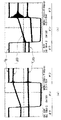
本実施形態の発光ダイオード駆動装置のスイッチング素子6がオフ→オン→オフした際の各部の電圧波形を図3(a)に示す。本実施形態と比較するため、図3(b)に、図13に示されるような従来の発光ダイオード駆動装置のスイッチング素子105がオフ→オン→オフした際の各部の電圧波形を示す。図3(a)及び図3(b)の縦軸は、スイッチング素子の両端子間電圧VDの波形、発光ダイオードに流れる電流ILEDの波形、発光ダイオードの両端子間電圧VLEDの波形を示している。スイッチング素子の両端子間電圧VDの波形の表示は20V/div、発光ダイオードに流れる電流ILEDの波形の表示は100mA/div、発光ダイオードの両端子間電圧VLEDの波形の表示は5V/divである。横軸は時間を示し、400ns/divである。
FIG. 3A shows voltage waveforms of the respective parts when the switching
図3(a)より明らかなように、本実施形態による発光ダイオード駆動装置はスイッチング素子6がオン/オフした瞬間に、発光ダイオード2の両端子間電圧VLEDは変動しない。一方、図3(b)より明らかなように、従来の発光ダイオード駆動装置はスイッチング素子がオンした瞬間に発光ダイオードの両端子間電圧VLEDは約9Vから約6Vに急峻に変動している。また、従来の発光ダイオード駆動装置はスイッチング素子がオフした瞬間に発光ダイオードの両端子間電圧VLEDは約8Vから約11Vに急峻に変動している。
As is clear from FIG. 3A, the voltage V LED between both terminals of the
本実施形態のようにスイッチング素子6と発光ダイオード2との間にチョークコイル3を接続すれば、スイッチング素子6がオン/オフを切り替えたときにチョークコイル3とスイッチング素子6の接続点L1の電位が大きく変動しても、発光ダイオード2の両端子間電位は大きく変動しない。そのため、発光ダイオードの寄生容量に大きな電流が充電されることは無い。
If the
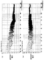
図4(a)に、本実施形態の発光ダイオード駆動装置が発生する雑音端子電圧波形を示す。本実施形態と比較するため、図4(b)に、図13に示されるような従来の発光ダイオード駆動装置が発生する雑音端子電圧波形を示す。図4(a)及び図4(b)の横軸はノイズ周波数を示し、縦軸は雑音端子電圧を示す。図4(a)及び図4(b)から明らかなように、本実施形態は、従来と比較して、1MHz以上の周波数領域におけるノイズレベルが顕著に低減している。 FIG. 4A shows a noise terminal voltage waveform generated by the light emitting diode driving apparatus of the present embodiment. For comparison with the present embodiment, FIG. 4B shows a noise terminal voltage waveform generated by a conventional light emitting diode driving device as shown in FIG. 4A and 4B, the horizontal axis indicates the noise frequency, and the vertical axis indicates the noise terminal voltage. As is clear from FIGS. 4A and 4B, in the present embodiment, the noise level in the frequency region of 1 MHz or more is significantly reduced as compared with the conventional example.
本実施形態のようにスイッチング素子6と発光ダイオード2との間にチョークコイル3を接続すれば、スイッチング素子6がオン/オフを切り替えたときに、発光ダイオード2の両端子間電位は大きく変動しない。そのため、発光ダイオード6がノイズ源にならず、直流電源1に伝達される雑音端子電圧を低減することができる。
If the
なお、発光ダイオード2を静電気破壊から保護する素子を、発光ダイオード2と並列に発光ダイオードの両端子に接続しても良い。例えば、静電破壊防止用として、発光ダイオード2と並列にコンデンサを接続しても良いし、発光ダイオード2と逆並列にツェナーダイオードを接続しても良い。又は、予めコンデンサやツェナーダイオードなどの静電破壊防止素子が発光素子と共に挿入されている発光ダイオード製品を使用しても良い。このような場合であっても、本実施形態と同様の効果が得られる。
An element that protects the
なお本実施形態の図1においては、電圧源としての直流電源1を使用したが、これに限定されるものではなく、交流電源と交流電圧を整流する整流回路を使用してもよい。また整流回路の高電位側と低電位側に平滑コンデンサを接続しても良い。以降に示す実施の形態においても同様である。
In FIG. 1 of the present embodiment, the
《第2の実施形態》
図5及び図6を用いて、本発明の第2の実施形態の発光ダイオード駆動装置について説明する。図5に、第2の実施形態の発光ダイオード駆動装置を示す。第2の実施形態の発光ダイオード駆動装置に含まれる構成要素は、第1の実施形態の発光ダイオード駆動装置に含まれる構成要素と同一であるが、各構成要素の接続関係が以下のように異なる。
<< Second Embodiment >>
A light-emitting diode driving device according to a second embodiment of the present invention will be described with reference to FIGS. FIG. 5 shows a light-emitting diode driving apparatus according to the second embodiment. The components included in the light-emitting diode driving device of the second embodiment are the same as those included in the light-emitting diode driving device of the first embodiment, but the connection relationship of each component is different as follows. .
本実施形態のスイッチング駆動回路5のスイッチング素子6は、一端を直流電源1の高電位側端子に接続され、他端をチョークコイル3の一端に接続される。チョークコイル3の他端は発光ダイオード2のアノード端子に接続される。整流ダイオード4は、カソード端子をスイッチング素子6とチョークコイル3との間に接続され、アノード端子を発光ダイオード2のカソード端子に接続される。発光ダイオード2のカソード端子と整流ダイオード4のアノード端子は、直流電源1の低電位側端子に接続される。
The switching
次に、本実施形態の発光ダイオード駆動装置の動作を図6を参照して説明する。図6は、上から、直流電源1の出力電圧VINの波形、スイッチング素子6の低電位側端子と基準電位端子間の電圧VSの波形、スイッチング素子6に流れる電流IDの波形、発光ダイオード2に流れる電流ILEDの波形、発光ダイオード2の順方向電圧VLEDの波形(すなわちアノード端子とカソード端子の電圧差波形)をそれぞれ表している。
Next, the operation of the light emitting diode driving device of the present embodiment will be described with reference to FIG. 6 shows, from above, the waveform of the output voltage VIN of the
制御回路ブロック7で決定された所望のタイミングに基づいてスイッチング素子6がオンすると、直流電源1の出力電圧VINがチョークコイル3及び発光ダイオード2に印加される。スイッチング素子6の低電位側端子と基準電位間の電圧VSの波形は、スイッチング素子6のオン電圧Von分だけ低下した電圧(VIN−Von)になる。スイッチング素子6→チョークコイル3→発光ダイオード2の経路に電流が流れ、発光ダイオード2に流れる電流ILEDの波形は、直流電源1の出力電圧VINとチョークコイル3のインダクタンス値Lで決定される、時間と共に増加する傾きを持った波形となる。
When the switching
スイッチング素子6がオフすると、直流電源1の出力電圧VINの印加が遮断されるため、チョークコイル3に逆起電力が発生する。この逆起電力によりチョークコイル3→発光ダイオード2→整流ダイオード4→チョークコイル3の経路に電流が流れる。発光ダイオード2に流れる電流ILEDの波形は、整流ダイオード4の順方向電圧VFと発光ダイオード2の順方向電圧VLEDの合計電圧(VF+VLED)とチョークコイル3のインダクタンス値Lで決定される、時間と共に減少する傾きをもった波形となる。
When the switching
発光ダイオード2のカソード端子は直流電源1の低電位側端子に接続されており、常に基準電位である。
The cathode terminal of the
スイッチング素子6がオンすると、スイッチング素子6とチョークコイル3の接続点L1の電圧は直流電源の出力電圧VINからスイッチング素子6のオン電圧Von分低下した電圧(VIN−Von)まで上昇する。
When the switching
一方、チョークコイル3と発光ダイオード2の接続点L2の電圧は、スイッチング素子6がオフしている間に、チョークコイル3の逆起電力によって発光ダイオード2に流れる電流ILEDにより発生している電位差(発光ダイオード2の順方向電圧VLED)で固定されている。そのため、スイッチング素子6がオンした瞬間に発光ダイオード2の両端子間の電位が大きく変動することはない。スイッチング素子6がオンの間、発光ダイオード2の順方向電圧VLEDは、発光ダイオード2に流れる電流ILEDの増加に伴い緩やかに増加するため、発光ダイオード2の両端子間電位差は緩やかに広がる。
On the other hand, the voltage at the connection point L2 between the
スイッチング素子6がオフすると、チョークコイル3に発生する逆起電力によってチョークコイル3の両端子間電位差は、発光ダイオード2の順方向電圧VLEDと整流ダイオード4の順方向電圧VFの合計値(VLED+VF)となる。チョークコイル3と発光ダイオード2の接続点L2の電圧は、直流電源1の基準電位から発光ダイオード2の順方向電圧VLEDだけ高い電圧(VLED)で固定されているため、スイッチング素子6とチョークコイル3の接続点L1の電圧は、接続点L2の電圧(VLED)からチョークコイル3の両端子に発生する電位差分(VLED+VF)を引いた電圧(−VF)まで瞬時に降下する。
When the switching
しかし、接続点L2の電圧は、直流電源1の基準電位から発光ダイオード2の順方向電圧VLEDだけ高い電圧(VLED)で固定されているため、スイッチング素子6がオフした瞬間に発光ダイオード2の両端子電位は大きく変動しない。スイッチング素子6がオフの間、発光ダイオード2の順方向電圧VLEDは、発光ダイオード2に流れる電流ILEDの減少に伴い緩やかに減少するため、発光ダイオード2の両端子間電位差は緩やかに狭まる。
However, since the voltage at the connection point L2 is fixed at a voltage (V LED ) that is higher than the reference potential of the
このように、スイッチング素子6のオン/オフが切り替わるとき、スイッチング素子6の低電位側端子と基準電位間の電圧VSが大きく変動しても、発光ダイオード2の両端子間電位VLEDは大きく変動しないため、発光ダイオードの寄生容量に大きな電流は充電されない。発光ダイオード6がノイズ源となることはなく、直流電源1に伝達される雑音端子電圧を低減することができる。
As described above, when the switching
また、本実施形態では、発光ダイオード2がスイッチング駆動回路5の低電位側と直流電源1の基準電位との間に接続されているため、発光ダイオード2のカソード端子の電圧は基準電位に固定される。発光ダイオード2のアノード端子には、発光ダイオード2の順方向電圧VLED以上の電圧が印加されないため、発光ダイオードの取り外し、取替え時に安全に作業することができる。
In this embodiment, since the
なお、静電破壊防止用としてコンデンサを発光ダイオード2と並列に接続した場合や、発光ダイオード2と逆並列にツェナーダイオードを接続した場合、又は予めコンデンサやツェナーダイオードなどの静電破壊防止素子が挿入されている発光ダイオード製品を使用した場合にも本実施形態と同様の効果が得られる。
In addition, when a capacitor is connected in parallel with the
《第3の実施形態》
図7及び図8を用いて、本発明の第3の実施形態の発光ダイオード駆動装置について説明する。図7に、第3の実施形態の発光ダイオード駆動装置を示す。第3の実施形態は、第1の実施形態の制御回路ブロック7の一例を具体的に示すものである。
<< Third Embodiment >>
A light emitting diode driving apparatus according to a third embodiment of the present invention will be described with reference to FIGS. FIG. 7 shows a light-emitting diode driving apparatus according to the third embodiment. The third embodiment specifically shows an example of the
また、第3の実施形態における電圧源は第1の実施形態と異なり、交流電圧を発生する交流電源8を用い、交流電源8に整流回路9が接続される。整流回路9は、本実施形態において全波整流回路であり、全波整流した直流電圧VINを出力する。整流回路9の高電位側は、発光ダイオード2のアノード端子と整流ダイオード4のカソード端子に接続され、整流回路9の低電位側はスイッチング駆動回路5の低電位側端子GND−SRCEに接続される。
Also, unlike the first embodiment, the voltage source in the third embodiment uses an
本実施形態のスイッチング駆動回路5は、入力端子IN、高電位側端子DRN、低電位側端子GND−SRCE、及び基準電圧端子VCCを有する。入力端子INは、整流回路9の高電位側に接続され、直流電圧VINを印加される。高電位側端子DRNは、チョークコイル3と整流ダイオード4のアノード端子の接続点に接続される。低電位側端子GND−SRCEは、制御回路ブロック7のグランド端子GNDと接続されてグランド電位(基準電位)となる。本実施形態の発光ダイオード駆動装置において、基準電圧端子VCCと低電位側端子GND−SRCEとの間にコンデンサ10が接続される。
The switching
スイッチング駆動回路5は、スイッチング素子6と制御回路ブロック7とを有する。スイッチング素子6は、高電位側端子DRNと低電位側端子GND−SRCEとの間に接続される。スイッチング素子6の制御端子は、制御回路ブロック7の出力端子GATEに接続される。
The switching
本実施形態の制御回路ブロック7は、直流電圧VINを入力し一定の基準電圧VCCをし出力するための定電流源14及びレギュレータ19、スイッチング素子6に流れる電流を検出する電流検出回路12、基準電圧VCCを印加されて駆動し、電流検出回路12の出力に基づいてスイッチング素子6のオン/オフを制御する制御回路70、並びに、直流電圧VINに基づいて制御回路70の動作を制限する入力電圧検出回路18及び起動/停止回路11、を有する。制御回路ブロック7は、さらにスイッチング駆動回路5の入力端子INに接続された入力端子VJを有する。
The
定電流源14は入力端子VJとレギュレータ19の一端との間に接続される。なお、定電流源14に接続される入力端子VJは、スイッチング駆動回路5の入力端子INの代わりに高電位側端子DRNに接続されても良い。定電流源14は電圧VJをレギュレータ19に出力する。
The constant
レギュレータ19の他端は基準電圧端子VCCに接続され、基準電圧端子VCCに基準電圧Vccを出力する。レギュレータ19は、電圧VJを所定の電圧値である起動電圧(図8の起動電圧VCC0)と比較して、電圧VJが起動電圧より小さければ電圧VJをそのまま基準電圧Vccとして出力し、電圧VJが起動電圧VCC0以上であれば一定の電圧値VCC0の基準電圧Vccを出力する。基準電圧Vccはコンデンサ14に蓄積される。制御回路ブロック7の内部回路は、基準電圧Vccが電圧値VCC0に達すると動作を開始する。
The other end of the
さらに、レギュレータ19は電圧VJが起動電圧VCC0よりも小さければ、停止信号であるロウ(L)信号を起動/停止回路11に出力し、起動/停止回路11がスイッチング素子6のオン/オフ制御を開始しないように制御する。また、レギュレータ19は電圧VJが起動電圧VCC0以上であれば、起動信号であるハイ(H)信号を起動/停止回路11に出力し、起動/停止回路11がスイッチング素子6のオン/オフ制御を開始するように制御する。
Further, the
制御回路ブロック7は、さらにグランド電位となるグランド端子GNDを有する。グランド端子GNDは、スイッチング駆動回路5の低電位側端子GND−SRCEに接続される。
The
入力電圧検出回路18は、入力端子INとグランド端子GNDとの間に直列に接続された抵抗15及び抵抗16と、抵抗15及び抵抗16の中間接続点の電圧を所定値である入力基準電圧Vstと比較するコンパレータ17とを有する。抵抗15及び抵抗16は、入力端子INに入力された直流電圧VINを分圧し、分圧電圧VIN18を出力する。コンパレータ17のプラス入力端子は、抵抗15及び抵抗16の中間接続点に接続されて、分圧電圧VIN18を入力する。コンパレータ17のマイナス入力端子は、入力基準電圧Vstを入力する。コンパレータ17は分圧電圧VIN18が入力基準電圧Vstより小さければロウ(L)信号を出力し、分圧電圧VIN18が入力基準電圧Vst以上であればハイ(H)信号を出力する。入力電圧検出回路18の出力するロウ信号は、発光ダイオード2を消光させるための消光信号であり、ハイ信号は発光ダイオード2を発光させるための発光信号である。コンパレータ17の出力端子は起動/停止回路11に接続される。
The input voltage detection circuit 18 includes a
起動/停止回路11は、レギュレータ19と入力電圧検出回路18のコンパレータ17の出力端子から出力される信号を入力する。起動/停止回路11の出力は、制御回路70のAND回路20に接続される。起動/停止回路11は、レギュレータ19から停止信号を入力している間は停止信号をAND回路20に出力し、レギュレータ19から起動信号を入力している間は入力電圧検出回路18の発光信号又は消光信号をAND回路20に出力する。すなわち、起動/停止回路11は、レギュレータ19と入力電圧検出回路18から入力された信号が両方ハイ信号のときにハイ信号を出力し、入力された信号のいずれかがロウ信号であればロウ信号を出力する。
The start /
電流検出回路12は、プラス入力端子を高電位側端子DRNに接続されて、スイッチング素子6のオン電圧Vonを入力し、マイナス入力端子に基準となる検出基準電圧Vsnを入力するコンパレータである。電流検出回路12は、オン電圧Vonが検出基準電圧Vsnよりも小さければロウ信号を出力し、オン電圧Vonが検出基準電圧Vsn以上であればハイ信号を出力する。スイッチング素子6のオン電圧Vonを電流検出回路12の検出基準電圧Vsnと比較することにより、スイッチング素子6に流れる電流IDは検出される。
The
制御回路70は、発振器13、AND回路20及び24、OR回路23、RSフリップフロップ回路22、及びオン時ブランキングパルス発生器21を有する。
The
発振器13は、マックスデューティ信号MXDTYとクロック信号CLKとを出力する。スイッチング素子6の発振周波数及びMAXオンデューティーは、発振器13のクロック信号CLK及びマックスデューティ信号MXDTYにより規定される。
The
AND回路24の入力端子は、電流検出回路12の出力端子とオン時ブランキングパルス発生器14の出力端子に接続され、AND回路24の出力端子はOR回路23の一方の入力端子に接続される。
The input terminal of the AND
OR回路23は他方の入力端子には、発振器13のマックスデューティ信号MXDTYの反転信号が入力される。
The OR
RSフリップフロップ回路22は、リセット信号端子RをOR回路23の出力端子に接続され、セット信号端子Sに発振器13のクロック信号CLKを入力される。
In the RS flip-
AND回路20の入力端子は、起動/停止回路11と、発振器13のマックスデューティ信号MXDTYを出力する出力端子と、RSフリップフロップ回路22の出力端子Qに接続される。
The input terminal of the AND
制御回路ブロック7は、スイッチング素子6の制御端子に接続される出力端子GATEを有し、AND回路20の出力端子が出力端子GATEに接続される。
The
オン時ブランキングパルス発生器21は、一端をAND回路20と出力端子GATEとの接続点に接続される。オン時ブランキングパルス発生器21は、AND回路20の出力信号を入力し、スイッチング素子6がオフからオンに切り替わってからある一定の時間(例えば数百nsec)ロウ信号を出力する。オン時ブランキングパルス発生器21は、それ以外はハイ信号を出力する。本実施形態は、オン時ブランキングパルス発生器21の出力信号と電流検出回路12の出力信号をAND回路24に入力することで、スイッチング素子6のオフ状態からオン状態に移行するときに発生するリンギングによるスイッチング素子6のオン/オフ制御の誤動作を防いでいる。
One end of the on-time blanking
次に、図8を用いて、本実施形態の発光ダイオード駆動装置の動作を説明する。図8は本実施形態の発光ダイオード駆動装置における、整流回路9の出力する直流電圧VINの波形と、発光ダイオード2に流れる電流ILEDの波形と、基準電圧VCCの波形を示した図である。図8の横軸は、時間である。整流回路9の出力する直流電圧VINは、図8のように交流電圧を全波整流した波形となる。
Next, the operation of the light emitting diode driving apparatus of the present embodiment will be described with reference to FIG. FIG. 8 is a diagram showing the waveform of the direct current voltage VIN output from the rectifier circuit 9, the waveform of the current I LED flowing through the
直流電圧VINが入力端子INを介して入力端子VJに印加されると、定電流源14の出力する電圧VJは電圧VINの上昇とともに上昇する。電圧VJが上昇すると、レギュレータ19により基準電圧Vccは上昇する。基準電圧Vccが起動電圧VCC0に達するまでの間、レギュレータ19は停止信号であるロウ信号を起動/停止回路11に出力しているため、スイッチング素子6のオン/オフ制御は行われない(停止期間T3)。
When the DC voltage V IN is applied to the input terminal VJ through the input terminal IN, the voltage V J to the output of the constant
電圧VJが起動電圧VCC0に達すると、レギュレータ19は電圧値VCC0の基準電圧Vccを出力し、制御回路ブロック7の内部回路は動作を開始する(起動期間T4)。発振器13はマックスデューティ信号MXDTYとクロック信号CLKの出力を開始する。レギュレータ19は起動信号であるハイ信号を起動/停止回路11に出力する。これによりスイッチング素子6の制御が開始される。すなわち起動/停止回路11は入力電圧検出回路18から出力される発光信号又は消光信号に基づいて、発光ダイオード2の発光期間T1又は消光期間T2を制御する。
When the voltage V J reaches the activation voltage V CC0, the
入力電圧検出回路18のコンパレータ17は分圧電圧VIN18が入力基準電圧Vstに達すると、起動/停止回路11に発光信号としてハイ信号を出力し、起動/停止回路11はハイ信号をAND回路20に出力する(発光期間T1)。これにより、制御回路70によるスイッチング素子6のオン・オフが制御され、発光ダイオード2は発光する。
When the divided voltage VIN18 reaches the input reference voltage Vst, the
本実施形態において、電圧VJが電圧値VCC0に達する時の電圧VINの電圧値VIN2よりも分圧電圧VIN18が基準電圧Vstに達する時の電圧VINの電圧値VIN1のほうが高くなるように設定する。 In the present embodiment, it is better voltage V IN of the voltage value V IN1 when the voltage V J is divided voltage V IN18 than the voltage value V IN2 of the voltage V IN when reaching the voltage value V CC0 reaches the reference voltage Vst Set to be higher.
入力電圧検出回路18のコンパレータ17は、分圧電圧VIN18が入力基準電圧Vstを下回ると、起動/停止回路11に消光信号としてロウ信号を出力し、起動/停止回路11はロウ信号をAND回路20に出力する(消光期間T2)。これによりスイッチング素子6はオフ状態に保たれ、発光ダイオード2は消光する。
When the divided voltage VIN18 falls below the input reference voltage Vst, the
すなわち、分圧電圧VIN18が入力基準電圧Vst以上の発光期間T1に、スイッチング素子6の断続的なオン/オフ制御は実行され、発光ダイオード2は発光する。分圧電圧VIN18が入力基準電圧Vst以下の消光期間T2に、スイッチング素子6のオン/オフ制御は停止され、発光ダイオード2は消光する。定電流ILEDは発光期間T1に発光ダイオード2に流れ、消光期間T2には流れない。
That is, intermittent ON / OFF control of the
レギュレータ19の出力する基準電圧Vccはコンデンサ10に蓄積される。レギュレータ19は電圧VJが起動電圧VCC0以上になる起動期間T4の間、基準電圧Vccが常に一定の電圧VCC0になるように制御する。また、レギュレータ19は、電圧VINが小さくなり電圧VJが再度電圧値VCC0よりも小さくなる起動期間T5において、基準電圧Vccが低下しないようにコンデンサ10の容量値を適切に設定する。基準電圧Vccが起動電圧VCC0に保たれている起動期間T4及びT5の間、スイッチング素子6のオン/オフ制御がなされ、発光ダイオード2は発光/消光を繰り返す。
The reference voltage Vcc output from the
次に、発光期間T1における、本実施形態の発光ダイオード駆動装置の定電流出力動作について説明する。発光期間T1における各電圧・各電流の波形は、図2のようになる。図2は、直流電源1の出力する直流電圧VINの波形、スイッチング素子6の高電位側端子と基準電位間の電圧VDの波形、スイッチング素子6に流れる電流IDの波形、発光ダイオード2に流れる電流ILEDの波形、発光ダイオード2の順方向電圧VLEDの波形(すなわちアノード端子とカソード端子の電圧差波形)を示す。
Next, the constant current output operation of the light emitting diode driving device of the present embodiment during the light emission period T1 will be described. The waveforms of the voltages and currents in the light emission period T1 are as shown in FIG. 2 shows the waveform of the DC voltage VIN output from the
発光期間T1における、スイッチング素子6の発振周波数及びMAXオンデューティーは、発振器13のクロック信号CLK及びマックスデューティ信号MXDTYにより規定される。
The oscillation frequency and the MAX on duty of the
スイッチング素子6がオンの間、スイッチング素子6の電圧VDは電圧値Vonとなる。オン電圧Vonが電圧値Vsnに達すると、電流検出回路12はハイレベルの信号を出力する。このハイレベルの信号は、AND回路24を介してOR回路23に入力され、OR回路23はハイレベルの信号を出力する。また、オン電圧Vonが電圧値Vsnに達しなくても、マックスデューティ信号MXDTYの反転信号がハイレベルとなると、OR回路23はハイレベルの信号を出力する。このハイレベルの信号は、RSフリップフロップ22のリセット信号端子Rに入力される。RSフリップフロップ22はリセットし、AND回路20にロウレベルの信号を出力する。AND回路20がロウレベルの信号を出力することにより、スイッチング素子6はオフ状態になる。
While the switching
発振器13のクロック信号CLKがRSフリップフロップ22のセット信号端子Sに入力されると、スイッチング素子6はオン状態になる。
When the clock signal CLK of the
オン時ブランキングパルス発生器21は、スイッチング素子6がオフからオンに切り替わってからある一定の時間ロウ信号を出力する。ロウ信号は、AND回路24に入力されるため、スイッチング素子6のオン/オフの制御は、電流検出回路12の出力信号に影響されない。一定の時間が経過すると、オン時ブランキングパルス発生器21はハイ信号を出力する。スイッチング素子6のオン/オフは、電流検出回路12の出力信号に基づいて、制御される。
The on-time blanking
スイッチング素子6のオン電圧Vonが電圧値Vsnに達するか、又はマックスデューティ信号MXDTYの反転信号がハイレベルとなると、OR回路23はハイレベルの信号を出力し、RSフリップフロップ22はリセットする。これにより、再びスイッチング素子6はオフ状態になる。
When the ON voltage Von of the
即ち、スイッチング素子6のオンデューティーは、発振器13のマックスデューティ信号MXDTYの反転信号と電流検出回路12の出力信号が入力されたOR回路23の出力信号により規定される。
That is, the on-duty of the
以上のように、制御回路ブロック7によるスイッチング素子6の断続的なオン/オフ制御が図8の発光期間T1になされると、発光ダイオード2に流れる電流ILEDは図2に示すようになる。
As described above, when intermittent ON / OFF control of the
スイッチング素子6がオンのとき、発光ダイオード2→チョークコイル3→スイッチング素子6の向きに電流ILEDが発光ダイオード2に流れる。スイッチング素子6がオフのとき、電流ILEDはチョークコイル3→整流ダイオード4→発光ダイオード2の閉ループを流れる。そのため、チョークコイル3に流れる電流(即ち、発光ダイオード2に流れる電流)は図2の電流ILEDに示すような波形となる。
When the switching
発光ダイオード2の順方向電圧VLEDは、スイッチング素子6がオンのとき発光ダイオード2に流れる電流ILEDの増加に伴い緩やかに増加し、スイッチング素子6がオフのとき発光ダイオード2に流れる電流ILEDの減少に伴い緩やかに減少する。
Forward voltage V LED of the
スイッチング素子6がオンしたとき、チョークコイル3とスイッチング素子6の接続点L1の電圧は、スイッチング素子6のオン電圧Vonまで低下する。しかし、発光ダイオード2とチョークコイル3の接続点L2の電圧は、大きく変動しないため、スイッチング素子6がオンした瞬間に、発光ダイオード2の両端子電位が大きく変動することはない。
When the switching
スイッチング素子6がオフしたとき、チョークコイル3に発生する逆起電力により、チョークコイルの両端子間電位差は発光ダイオード2の順方向電圧VLEDと整流ダイオード4の順方向電圧VFの合計値(VLED+VF)となる。発光ダイオード2とチョークコイル3との接続点L2の電圧は、直流電源1の出力電圧VINから発光ダイオード2の順方向電圧VLEDだけ低下した電圧(VIN−VLED)で固定されているため、チョークコイル3とスイッチング素子6の接続点L1の電圧は、ダイオード2とチョークコイル3との接続点L2の電圧(VIN−VLED)にチョークコイル3の両端子に発生する電位差分(VLED+VF)を足した電圧(VIN+VF)まで瞬時に上昇する。しかし、発光ダイオード2とチョークコイル3の接続点L2の電圧は、大きく変動しないため、スイッチング素子6がオフした瞬間に発光ダイオード2の両端子電位が大きく変動することはない。
When the switching
本実施形態のようにスイッチング素子6と発光ダイオード2との間にチョークコイル3を接続すれば、スイッチング素子6がオン/オフを切り替えたときにチョークコイル3とスイッチング素子6の接続点L1の電位が大きく変動しても、発光ダイオード2の両端子間電位は大きく変動しない。そのため、発光ダイオードの寄生容量に大きな電流が充電されることは無い。また、発光ダイオード6がノイズ源にならず、直流電源1に伝達される雑音端子電圧を低減することができる。
If the
なお、図7においては、検出基準電圧Vsnは所定の電圧値であったが、検出基準電圧Vsnを外部から入力するための外部検出端子(図示せず)をスイッチング駆動回路5に設けても良い。この場合、検出基準電圧Vsnの電圧値を任意に設定し変更することにより、スイッチング素子6に流れる電流IDのピーク電流値を変えることができる。これにより、発光ダイオード2に流れる電流ILEDの電流値を変えることができ、調光機能を有する発光ダイオード駆動装置を実現できる。
In FIG. 7, the detection reference voltage Vsn has a predetermined voltage value. However, an external detection terminal (not shown) for inputting the detection reference voltage Vsn from the outside may be provided in the switching
また、入力基準電圧Vstは所定の電圧値であったが、入力基準電圧Vstを外部から入力するための外部接続端子(図示せず)をスイッチング駆動回路5に設けても良い。入力基準電圧Vsnの電圧値を任意に設定し変更することにより、発光ダイオード2に電流ILEDが流れる発光期間T1の長さを簡単に調整できる。
Although the input reference voltage Vst has a predetermined voltage value, an external connection terminal (not shown) for inputting the input reference voltage Vst from the outside may be provided in the switching
また、交流電源8に商用電源を使用した場合、倍周期中(100Hz/120Hz)で発光期間T1と消光期間T2を簡単に調整でき、白色発光ダイオードの色度と光度を簡単に調整できる。
When a commercial power source is used as the
本実施形態の発光ダイオード駆動装置を使用した場合、さらに以下の効果がある。本実施形態のスイッチング駆動回路は、電力供給のための抵抗が不要なため、起動時の電力損失がない。一般的に、スイッチング駆動回路に対する電力供給は、入力電圧(高電圧)から直流的に抵抗を介して行われる。この電力供給は起動・停止のみならず、通常動作中も同じように行われるため、抵抗での電力損失が発生する。しかし、本実施の形態の構成によれば、このような抵抗は不要である。 When the light emitting diode driving device of the present embodiment is used, the following effects are further obtained. Since the switching drive circuit of this embodiment does not require a resistor for supplying power, there is no power loss at the time of startup. In general, power is supplied to the switching drive circuit from an input voltage (high voltage) in a direct manner through a resistor. This power supply is performed not only during start / stop but also during normal operation, so that power loss occurs in the resistor. However, according to the configuration of the present embodiment, such a resistor is not necessary.
スイッチング素子6に流れる電流IDは、スイッチング素子6のオン電圧Vonを電流検出回路12により検出するため、従来のような電流を検出するための検出抵抗が不要となり、検出抵抗による電力損失は発生しない。
Since the current ID flowing through the switching
また、図7において、スイッチング駆動回路5中のスイッチング素子6と制御回路ブロック7を同一基板上に形成することで、発光ダイオード駆動装置の更なる小型化が実現できる。これは、以降に示す実施の形態においても同様である。
In FIG. 7, the switching
また、図7において、交流電圧を整流する手段として全波整流回路9を使用したが、半波整流回路を使用しても同様の効果が得られるのは明白である。これは、以降に示す実施の形態においても同様である。 In FIG. 7, the full-wave rectifier circuit 9 is used as means for rectifying the AC voltage. However, it is obvious that the same effect can be obtained even if a half-wave rectifier circuit is used. The same applies to the embodiments described below.
なお、スイッチング素子6の高電位側端子DRNと低電位側端子GND-SRCEにツェナーダイオードなどのクランプ回路を並列接続してもよい。制御回路ブロック7によるスイッチング素子6の断続的なオン/オフ制御において、スイッチング素子6がオン状態からオフ状態へ移行するときに、スイッチング素子6の高電位側電圧VDが、配線容量や配線インダクタンスで生ずるリンギングによりスイッチング素子6の耐圧を超える電圧となる場合がある。この場合、スイッチング素子6の破壊につながるおそれがある。このような場合に、スイッチング素子6の耐圧よりも低いクランプ電圧を有するクランプ回路を並列に接続することで、スイッチング素子6の電圧VDをこのクランプ電圧でクランプし、スイッチング素子6の破壊を防ぐことが可能になる。これにより、更に安全性の高い発光ダイオード駆動装置を実現できる。以下の実施の形態においても同様に、クランプ回路を追加することで同様の効果を得ることができる。
A clamp circuit such as a Zener diode may be connected in parallel to the high potential side terminal DRN and the low potential side terminal GND-SRCE of the
なお、スイッチング素子6がオフ状態からオン状態に移行する過渡状態において、整流ダイオード4の逆回復時間(Trr)が遅いと電力損失が大きくなるため、本実施形態の整流ダイオード4の逆回復時間(Trr)は100nsec以下である。
Note that, in a transient state where the switching
《第4の実施形態》
図9を用いて、本発明の第4の実施形態の発光ダイオード駆動装置について説明する。図9に、第4の実施形態の発光ダイオード駆動装置を示す。第4の実施形態は、第2の実施形態の制御回路ブロック7の一例を具体的に示すものである。すなわち、スイッチング駆動回路5は、整流回路9の高電位側とチョークコイル3の一端との間に接続され、チョークコイル3の他端は発光ダイオード2のアノード端子に接続される。第4の実施形態の制御回路ブロック7の内部回路は、第3の実施形態の制御回路ブロック7の内部回路と同一である。
<< Fourth Embodiment >>
A light-emitting diode driving device according to a fourth embodiment of the present invention will be described with reference to FIG. FIG. 9 shows a light emitting diode driving apparatus according to the fourth embodiment. The fourth embodiment specifically shows an example of the
第4の実施形態における電圧源は第3の実施形態と同様に、交流電圧を発生する交流電源8を用い、交流電源8に整流回路9が接続される。整流回路9は、本実施形態において全波整流回路であり、全波整流した直流電圧VINを出力する。
As in the third embodiment, the voltage source in the fourth embodiment uses an
本実施形態において、整流回路9の高電位側は、スイッチング駆動回路5の入力端子IN及び高電位側端子DRNに接続される。スイッチング駆動回路5の低電位側端子GND−SRCEはチョークコイル3の一端と整流ダイオード4のカソード端子に接続される。チョークコイル3の他端は発光ダイオード2のアノード端子に接続される。発光ダイオード2のカソード端子と整流ダイオード4のアノード端子は整流回路9の低電位側端子に接続される。
In the present embodiment, the high potential side of the rectifier circuit 9 is connected to the input terminal IN and the high potential side terminal DRN of the switching
スイッチング駆動回路5の低電位側端子GND−SRCEは、制御回路ブロック7のグランド端子GNDに接続されて、スイッチング駆動回路5の基準電位となる。基準電圧端子VCCと低電位側端子GND−SRCEの間にコンデンサ10が接続される。
The low potential side terminal GND-SRCE of the switching
以上のように構成することにより、スイッチング駆動回路5を発光ダイオード2より高電位側に配置する回路構成においても、第3の実施形態と同一のスイッチング駆動回路7を使用することができる。本実施形態は、第3の実施形態と同様の効果を得ることができる。
With the configuration described above, the same
《第5の実施形態》
図10及び図11を用いて、本発明の第5の実施形態の発光ダイオード駆動装置について説明する。図10に、第5の実施形態の発光ダイオード駆動装置を示す。本実施形態の発光ダイオード駆動装置は、図7に示す第3の実施形態と比較して、以下の点が異なる。
<< Fifth Embodiment >>
A light emitting diode driving apparatus according to a fifth embodiment of the present invention will be described with reference to FIGS. FIG. 10 shows a light emitting diode driving apparatus according to the fifth embodiment. The light emitting diode driving device of this embodiment is different in the following points from the third embodiment shown in FIG.
本実施形態の発光ダイオード駆動装置は、入力端子INと整流回路9の間に接続される抵抗28を更に有する。
The light emitting diode driving device of the present embodiment further includes a
また、スイッチング駆動回路5は、入力端子INとは別に、直流電圧VINを抵抗28を介さずに入力するための入力端子JFETを有する。入力端子JFETに入力端子VJが接続され、定電流源14は直流電圧VINを入力する。
In addition to the input terminal IN, the switching
本実施形態の入力電圧検出回路27は、入力端子INとグランド端子GNDとの間に直列に接続された3つの抵抗29、30、31と、抵抗29と抵抗30の接続点から出力される第1の分圧電圧VH27をプラス入力端子に入力し、入力基準電圧Vstをマイナス入力端子に入力する第1のコンパレータ32と、抵抗30と抵抗31の接続点から出力される第2の分圧電圧VL27をマイナス入力端子に入力し、入力基準電圧Vstをプラス入力端子に入力する第2のコンパレータ33と、第1のコンパレータ32および第2のコンパレータ33の出力端子に入力端子を接続されるAND回路34を有する。AND回路34の出力端子は起動/停止回路11に接続される。ここで、第1の分圧電圧VH27と第2の分圧電圧VL27には、常にVH27>VL27の関係がある。
The input
本実施形態の制御回路ブロック7は、スイッチング素子25と抵抗26を更に有する。スイッチング素子25は、スイッチング素子6と並列に接続される。スイッチング素子25には、スイッチング素子6に流れる電流よりも小さい、一定の電流比の電流が流れる。スイッチング素子25の高電位側はスイッチング素子6の高電位側に接続される。スイッチング素子25の制御端子は、スイッチング素子6の制御端子と共通に制御回路ブロック7の出力端子GATEに接続される。抵抗26は、スイッチング素子25の低電位側とグランド端子GNDとの間に接続される。
The
電流検出回路12は、スイッチング素子25に流れる電流を抵抗26の両端の電圧で検出して、検出基準電圧Vsnと比較する。
The
本実施形態のスイッチング駆動回路5は外部検出端子SNをさらに有し、外部検出端子SNに入力される検出基準電圧Vsnを、電流検出回路12に出力する。
The switching
上記以外の構成については、本実施形態は、図7に示す第3の実施形態と同じである。 Regarding configurations other than those described above, the present embodiment is the same as the third embodiment shown in FIG.
このように構成される本実施形態の発光ダイオード駆動装置の動作について、図11を参照して説明する。図11は、発光ダイオード2に流れる電流ILED、第1の分圧電圧VH27、及び第2の分圧電圧VL27の波形を示す図であり、横軸は時間tを示す。
The operation of the light emitting diode driving apparatus of the present embodiment configured as described above will be described with reference to FIG. FIG. 11 is a diagram illustrating waveforms of the current I LED , the first divided voltage V H27 , and the second divided voltage V L27 that flow through the
第1の分圧電圧VH27が入力基準電圧Vstに達するまでの消光期間T2Aにおいて、第1のコンパレータ32は信号レベルがロウレベルの信号を出力する。一方、第2の分圧電圧VL27は入力基準電圧Vstよりも低いため、第2のコンパレータ33は信号レベルがハイレベルの信号を出力する。2つのコンパレータ32、33の出力信号が入力されるAND回路34の出力信号はロウレベルとなり、起動/停止回路11はAND回路13に消光信号であるロウ信号を出力する。制御回路ブロック7はスイッチング素子6の制御を停止する(消光期間T2A)。
In the extinction period T2A until the first divided voltage V H27 reaches the input reference voltage Vst, the
直流電圧VINが上昇し、第1の分圧電圧VH27が入力基準電圧Vstに達すると、第1のコンパレータ32は信号レベルがハイレベルの信号を出力する。一方、第2の分圧電圧VL27は入力基準電圧vstよりも低いため、第2のコンパレータ33は信号レベルがハイレベルの信号を出力する。2つのコンパレータ32、33の出力信号が入力されるAND回路34の出力信号はハイレベルとなり、起動/停止回路11はAND回路13に発光信号であるハイ信号を出力する。制御回路ブロック8によるスイッチング素子6の断続的なオン/オフ制御が開始され、発光ダイオードは発光する(発光期間T1)。
When the DC voltage VIN rises and the first divided voltage V H27 reaches the input reference voltage Vst, the
さらに直流電圧VINが上昇し、第2の分圧電圧VL27が入力基準電圧Vstに達すると、コンパレータ33は信号レベルがロウレベルの信号を出力する。一方、第1の分圧電圧VH27は入力基準電圧Vstよりも高いため、第1のコンパレータ32は信号レベルがハイレベルの信号を出力し続ける。2つのコンパレータ32、33の出力信号が入力されるAND回路34の出力信号はロウレベルとなり、起動/停止回路11はAND回路13に消光信号であるロウ信号を出力する。制御回路ブロック8はスイッチング素子6の制御を停止する(消光期間T2B)。
When the DC voltage VIN further increases and the second divided voltage V L27 reaches the input reference voltage Vst, the
その後、直流電圧VINが下降すると、再び第2の分圧電圧VL27は入力基準電圧Vstを下回り、スイッチング素子6は発振状態となる(発光期間T1)。
Thereafter, when the DC voltage VIN decreases, the second divided voltage V L27 again falls below the input reference voltage Vst, and the
そして、第1の分圧電圧VH27が入力基準電圧Vstを下回ると、スイッチング素子6は停止状態となる(消光期間T2A)。
When the first divided voltage V H27 falls below the input reference voltage Vst, the switching
すなわち、図11に示すように、第1の分圧電圧VH27が入力基準電圧Vstよりも小さい消光期間T2A、制御回路ブロック7はスイッチング素子6のオン/オフ制御を停止して、スイッチング素子6のオフ状態を保持するため、発光ダイオード2は消光する。一方、第1の分圧電圧VH27が入力基準電圧Vstよりも高く、かつ第2の分圧電圧VL27が入力基準電圧Vstよりも低い発光期間T1は、制御回路ブロック7によるスイッチング素子6のオン/オフ制御がなされ、発光ダイオードは発光する。さらに第2の分圧電圧VL27が入力基準電圧Vstよりも高い消光期間T2B、制御回路ブロック7はスイッチング素子6のオン/オフ制御を停止して、スイッチング素子6のオフ状態を保持するため、発光ダイオード2は消光する。
That is, as shown in FIG. 11, the extinction period T2A in which the first divided voltage V H27 is smaller than the input reference voltage Vst, the
本実施形態によれば、第1の実施形態及び第3の実施形態の効果に加え、さらに下記の効果を有する。直流電圧VINの変化に対して、スイッチング素子6のオン/オフ制御が可能となる電圧レベルの上限値と下限値を設定できる。入力電圧検出回路27は異常な高電圧が印加されたときの保護回路となり、本実施形態はより安全な発光ダイオード駆動装置を実現することができる。
According to this embodiment, in addition to the effects of the first embodiment and the third embodiment, the following effects are further obtained. With respect to the change of the DC voltage VIN , the upper limit value and the lower limit value of the voltage level at which the
また、抵抗28の抵抗値を変更することにより、直流電圧VINの変化に対して、スイッチング素子6のオン/オフ制御が可能な電圧レベルの上限値と下限値を任意に設定できる。これにより、より安全で複雑な光度調整が可能な発光ダイオード駆動装置を実現できる。また抵抗28に高抵抗を使用することにより、入力電圧検出回路27の抵抗29,30,31で発生する電力損失を少なくすることができる。
Further, by changing the resistance value of the
なお、本実施形態の入力電圧検出回路27は、3つの直列接続された抵抗を有し、第1の分圧電圧VH27と第2の分圧電圧VL27を生成したが、これに限らず、入力電圧検出回路27の内部構成は、直流電圧VINの変化に対して、スイッチング素子6のオン/オフ制御が可能となる電圧レベルの上限値と下限値を規定できるような構成とすればよい。
Although the input
また、抵抗28を使用しない場合は、入力端子INと入力端子JFETは共通化することができる。その場合、入力電圧検出回路27の抵抗29の高電位側と入力端子VJは同じ入力端子IN(又はJFET)に接続することができる。
When the
なお、整流回路9の高電位側と低電位側に平滑コンデンサ(図示せず)を接続しても良い。整流回路9の高電位側と低電位側に平滑コンデンサを追加した場合、直流電圧VINはあるリップル電圧幅を持った直流電圧とみなすことができる。このような場合、入力電圧検出回路27は整流回路9や平滑コンデンサが破壊して直流電圧VINが異常な電圧となったときに、スイッチング駆動回路5を停止させ、スイッチング駆動回路5を保護する保護回路として作用する。
A smoothing capacitor (not shown) may be connected to the high potential side and the low potential side of the rectifier circuit 9. When smoothing capacitors are added to the high potential side and the low potential side of the rectifier circuit 9, the DC voltage VIN can be regarded as a DC voltage having a certain ripple voltage width. In such a case, the input
なお、本実施形態における抵抗26及びスイッチング駆動回路5の内部回路の構成は、図9に示す第4の実施形態においても適用できる。
The configuration of the
《実施の形態6》
図12を用いて、本発明の第6の実施形態の発光ダイオード駆動装置について説明する。図12に、第6の実施形態の発光ダイオード駆動装置を示す。本実施形態の発光ダイオード駆動装置は、ソフトスタート回路35と調光用制御回路36とを追加したことが、図10に示す第5の実施形態と異なり、それ以外の構成については第5の実施形態と同様である。
<<
A light emitting diode driving apparatus according to a sixth embodiment of the present invention will be described with reference to FIG. FIG. 12 shows a light emitting diode driving apparatus according to the sixth embodiment. Unlike the fifth embodiment shown in FIG. 10, the light emitting diode driving apparatus of this embodiment is different from the fifth embodiment shown in FIG. 10 in that a
ソフトスタート回路35は、外部検出端子SNと電流検出回路12との間に接続される。ソフトスタート回路35は、起動/停止回路11とも接続される。ソフトスタート回路35は起動/停止回路11から発光信号であるハイ(H)信号を入力されると、検出基準電圧Vsnを一定値に至るまで徐々に増加するように出力する。以上のような構成にすることにより、起動時に発生する突入電流を防止できる。検出基準電圧Vsnを徐々に増加させることにより、発光ダイオード2に流れる電流ILEDを徐々に高くすることができる。これにより、発光ダイオードの光度を徐々に上げることができる。
The
調光用制御回路36は外部検出端子SNに接続される。調光用制御回路36として、例えば8ビットマイコンを使用した場合、外部からの信号に応じて256段階調光が可能になる。
The dimming
また、基準電圧端子VCCとグランド端子GNDとの間に、固定抵抗と可変抵抗を直列に接続し、2つの抵抗で分圧された電圧を外部検出端子SNに入力すると、可変抵抗値を変更することにより、無段階調光が可能となる。 Further, when a fixed resistor and a variable resistor are connected in series between the reference voltage terminal VCC and the ground terminal GND, and a voltage divided by the two resistors is input to the external detection terminal SN, the variable resistance value is changed. Thus, stepless dimming is possible.
本実施形態によれば、第1から第5の実施形態の効果に加え、さらに簡易な構成で調光機能を有する発光ダイオード駆動装置を実現するという有利な効果が得られる。 According to the present embodiment, in addition to the effects of the first to fifth embodiments, an advantageous effect of realizing a light emitting diode driving device having a dimming function with a simpler configuration can be obtained.
なお、本実施形態におけるソフトスタート回路35と調光用制御回路35は、図9に示す第4の実施形態においても適用できる。
The
本発明は、発光ダイオードを使用した装置・機器全般に利用可能であり、特にLED照明機器として有用である。 INDUSTRIAL APPLICABILITY The present invention can be used for all apparatuses and devices using light emitting diodes, and is particularly useful as an LED lighting device.
1 直流電源
2 発光ダイオード
3 チョークコイル
4 整流ダイオード
5 スイッチング駆動回路
6、25 スイッチング素子
7 制御回路ブロック
8 交流電源
9 整流回路
10 コンデンサ
11 起動/停止回路
12 電流検出回路
13 発振器
14 定電流源
15、16、26、28、29、30、31 抵抗
17、32、33 コンパレータ
18、27 入力電圧検出回路
19 レギュレータ
20、24、34 AND回路
21 オン時ブランキングパルス発生器
22 RSフリップフロップ
23 OR回路
35 ソフトスタート回路
36 調光用制御回路
70 制御回路
DESCRIPTION OF
12
18, 27 Input
Claims (10)
電圧源の高電位端子に配線のみを介して直接接続されたアノードと、前記チョークコイルの一端に配線のみを介して直接接続されたカソードとを有する少なくとも1つの発光ダイオードと、
前記チョークコイルの他端に接続されたアノードと、前記発光ダイオードのアノードに接続されたカソードとを有し、前記チョークコイルに発生する逆起電力を前記発光ダイオードに供給する整流ダイオードと、
前記発光ダイオードに流れる電流を制御するスイッチング駆動回路とを備え、
前記スイッチング駆動回路は、
前記チョークコイルの他端に接続されたドレインと、前記電圧源の低電位端子に接続されたソースと、ゲートとを有し、前記発光ダイオードへの電流の印加/非印加を決定するスイッチング素子と、
前記スイッチング素子のオン/オフのタイミングを制御して前記発光ダイオードに流れる電流を制御する制御回路ブロックとを備え、
前記制御回路ブロックは、
前記スイッチング素子のソースとドレインとの間の電圧を所定の検出基準電圧と比較することにより、前記スイッチング素子に流れる電流を検出する電流検出回路を備え、
前記電圧源は、交流電圧を出力する交流電源と、前記交流電圧を整流する整流回路とを備え、
前記制御回路ブロックは、
前記整流回路に一端を接続された定電流源と、
前記定電流源の他端に接続され、前記定電流源の出力電圧が所定値以上であれば起動信号を出力し、前記定電流源の出力電圧が所定値未満であれば停止信号を出力するレギュレータと、
前記発光ダイオードに流れる電流が一定になるように、前記電流検出回路の出力信号に基づいて前記スイッチング素子を所定の発振周波数で断続的にオン/オフ制御する制御回路と、
前記レギュレータからの起動信号及び停止信号に基づいて、前記制御回路の起動と停止を制御する起動/停止回路と、
を有することを特徴とする発光ダイオード駆動装置。 A choke coil,
At least one light-emitting diode having an anode directly connected to the high potential terminal of the voltage source through the wiring only; and a cathode directly connected to the one end of the choke coil through the wiring only;
A rectifier diode having an anode connected to the other end of the choke coil and a cathode connected to the anode of the light emitting diode, and supplying back electromotive force generated in the choke coil to the light emitting diode;
A switching drive circuit for controlling a current flowing through the light emitting diode,
The switching drive circuit is
A switching element having a drain connected to the other end of the choke coil, a source connected to a low potential terminal of the voltage source, and a gate, and determining application / non-application of current to the light emitting diode; ,
A control circuit block for controlling the current flowing in the light emitting diode by controlling the on / off timing of the switching element;
The control circuit block is
A current detection circuit that detects a current flowing through the switching element by comparing a voltage between a source and a drain of the switching element with a predetermined detection reference voltage ;
The voltage source includes an AC power source that outputs an AC voltage, and a rectifier circuit that rectifies the AC voltage ,
The control circuit block is
A constant current source having one end connected to the rectifier circuit;
Connected to the other end of the constant current source, outputs a start signal if the output voltage of the constant current source is greater than or equal to a predetermined value, and outputs a stop signal if the output voltage of the constant current source is less than a predetermined value. A regulator,
A control circuit for intermittently turning on / off the switching element at a predetermined oscillation frequency based on an output signal of the current detection circuit so that a current flowing through the light emitting diode is constant;
A start / stop circuit for controlling start and stop of the control circuit based on a start signal and a stop signal from the regulator;
LED driving device characterized by having a.
電圧源の高電位端子に配線のみを介して直接接続されたアノードと、前記チョークコイルの一端に配線のみを介して直接接続されたカソードとを有する少なくとも1つの発光ダイオードと、
前記チョークコイルの他端に接続されたアノードと、前記発光ダイオードのアノードに接続されたカソードとを有し、前記チョークコイルに発生する逆起電力を前記発光ダイオードに供給する整流ダイオードと、
前記発光ダイオードに流れる電流を制御するスイッチング駆動回路とを備え、
前記スイッチング駆動回路は、
前記チョークコイルの他端に接続されたドレインと、前記電圧源の低電位端子に接続されたソースと、ゲートとを有し、前記発光ダイオードへの電流の印加/非印加を決定するスイッチング素子と、
前記チョークコイルの他端と前記スイッチング素子のドレインとの間の接続点に接続されたドレインと、ソースと、前記スイッチング素子のゲートに接続されたゲートとを有し、かつ前記スイッチング素子に流れる電流よりも小さくかつ前記スイッチング素子に流れる電流に対して一定の電流比の電流が流れる他のスイッチング素子と、
前記スイッチング素子及び前記他のスイッチング素子が連動してオン/オフするように当該オン/オフのタイミングを制御して前記発光ダイオードに流れる電流を制御する制御回路ブロックとを備え、
前記制御回路ブロックは、
前記他のスイッチング素子のソースに接続された一端と、前記電圧源の低電位端子に接続された他端とを有する電流検出抵抗と、
前記電流検出抵抗の両端電圧を所定の検出基準電圧と比較することにより、前記スイッチング素子に流れる電流を検出する電流検出回路とを備え、
前記電圧源は、交流電圧を出力する交流電源と、前記交流電圧を整流する整流回路とを備え、
前記制御回路ブロックは、
前記整流回路に一端を接続された定電流源と、
前記定電流源の他端に接続され、前記定電流源の出力電圧が所定値以上であれば起動信号を出力し、前記定電流源の出力電圧が所定値未満であれば停止信号を出力するレギュレータと、
前記発光ダイオードに流れる電流が一定になるように、前記電流検出回路の出力信号に基づいて前記スイッチング素子を所定の発振周波数で断続的にオン/オフ制御する制御回路と、
前記レギュレータからの起動信号及び停止信号に基づいて、前記制御回路の起動と停止を制御する起動/停止回路と、
を有することを特徴とする発光ダイオード駆動装置。 A choke coil,
At least one light-emitting diode having an anode directly connected to the high potential terminal of the voltage source through the wiring only; and a cathode directly connected to the one end of the choke coil through the wiring only;
A rectifier diode having an anode connected to the other end of the choke coil and a cathode connected to the anode of the light emitting diode, and supplying back electromotive force generated in the choke coil to the light emitting diode;
A switching drive circuit for controlling a current flowing through the light emitting diode,
The switching drive circuit is
A switching element having a drain connected to the other end of the choke coil, a source connected to a low potential terminal of the voltage source, and a gate, and determining application / non-application of current to the light emitting diode; ,
A drain having a drain connected to a connection point between the other end of the choke coil and the drain of the switching element, a source, and a gate connected to the gate of the switching element, and flowing through the switching element Other switching elements that are smaller than and flow a current with a constant current ratio with respect to the current that flows through the switching elements;
A control circuit block for controlling the current flowing in the light emitting diode by controlling the on / off timing so that the switching element and the other switching element are turned on / off in conjunction with each other;
The control circuit block is
A current detection resistor having one end connected to the source of the other switching element and the other end connected to the low potential terminal of the voltage source;
A current detection circuit that detects a current flowing through the switching element by comparing a voltage across the current detection resistor with a predetermined detection reference voltage ;
The voltage source includes an AC power source that outputs an AC voltage, and a rectifier circuit that rectifies the AC voltage ,
The control circuit block is
A constant current source having one end connected to the rectifier circuit;
Connected to the other end of the constant current source, outputs a start signal if the output voltage of the constant current source is greater than or equal to a predetermined value, and outputs a stop signal if the output voltage of the constant current source is less than a predetermined value. A regulator,
A control circuit for intermittently turning on / off the switching element at a predetermined oscillation frequency based on an output signal of the current detection circuit so that a current flowing through the light emitting diode is constant;
A start / stop circuit for controlling start and stop of the control circuit based on a start signal and a stop signal from the regulator;
LED driving device characterized by having a.
電圧源の高電位端子に配線のみを介して直接接続されたアノードと、前記チョークコイルの一端に配線のみを介して直接接続されたカソードとを有する少なくとも1つの発光ダイオードと、
前記チョークコイルの他端に接続されたアノードと、前記発光ダイオードのアノードに接続されたカソードとを有し、前記チョークコイルに発生する逆起電力を前記発光ダイオードに供給する整流ダイオードと、
前記発光ダイオードに流れる電流を制御するスイッチング駆動回路とを備え、
前記スイッチング駆動回路は、
前記チョークコイルの他端に接続されたドレインと、前記電圧源の低電位端子に接続されたソースと、ゲートとを有し、前記発光ダイオードへの電流の印加/非印加を決定するスイッチング素子と、
前記スイッチング素子のオン/オフのタイミングを制御して前記発光ダイオードに流れる電流を制御する制御回路ブロックとを備え、
前記制御回路ブロックは、
前記スイッチング素子に流れる電流に対応する電圧を所定の検出基準電圧と比較することにより、前記スイッチング素子に流れる電流を検出する電流検出回路と、
一定値に至るまで徐々に増加するように、前記検出基準電圧を発生して前記電流検出回路に出力するソフトスタート回路とを備え、
前記電圧源は、交流電圧を出力する交流電源と、前記交流電圧を整流する整流回路とを備え、
前記制御回路ブロックは、
前記整流回路に一端を接続された定電流源と、
前記定電流源の他端に接続され、前記定電流源の出力電圧が所定値以上であれば起動信号を出力し、前記定電流源の出力電圧が所定値未満であれば停止信号を出力するレギュレータと、
前記発光ダイオードに流れる電流が一定になるように、前記電流検出回路の出力信号に基づいて前記スイッチング素子を所定の発振周波数で断続的にオン/オフ制御する制御回路と、
前記レギュレータからの起動信号及び停止信号に基づいて、前記制御回路の起動と停止を制御する起動/停止回路と、
を有することを特徴とする発光ダイオード駆動装置。 A choke coil,
At least one light-emitting diode having an anode directly connected to the high potential terminal of the voltage source through the wiring only; and a cathode directly connected to the one end of the choke coil through the wiring only;
A rectifier diode having an anode connected to the other end of the choke coil and a cathode connected to the anode of the light emitting diode, and supplying back electromotive force generated in the choke coil to the light emitting diode;
A switching drive circuit for controlling a current flowing through the light emitting diode,
The switching drive circuit is
A switching element having a drain connected to the other end of the choke coil, a source connected to a low potential terminal of the voltage source, and a gate, and determining application / non-application of current to the light emitting diode; ,
A control circuit block for controlling the current flowing in the light emitting diode by controlling the on / off timing of the switching element;
The control circuit block is
A current detection circuit for detecting a current flowing through the switching element by comparing a voltage corresponding to the current flowing through the switching element with a predetermined detection reference voltage;
A soft start circuit that generates the detection reference voltage and outputs it to the current detection circuit so as to gradually increase until reaching a certain value ;
The voltage source includes an AC power source that outputs an AC voltage, and a rectifier circuit that rectifies the AC voltage ,
The control circuit block is
A constant current source having one end connected to the rectifier circuit;
Connected to the other end of the constant current source, outputs a start signal if the output voltage of the constant current source is greater than or equal to a predetermined value, and outputs a stop signal if the output voltage of the constant current source is less than a predetermined value. A regulator,
A control circuit for intermittently turning on / off the switching element at a predetermined oscillation frequency based on an output signal of the current detection circuit so that a current flowing through the light emitting diode is constant;
A start / stop circuit for controlling start and stop of the control circuit based on a start signal and a stop signal from the regulator;
LED driving device characterized by having a.
前記起動/停止回路は、前記レギュレータが停止信号を出力している場合は前記停止信号を前記制御回路に出力し、前記レギュレータが起動信号を出力している場合は、前記入力電圧検出回路の発光信号又は消光信号を前記制御回路に出力することを特徴とする請求項1から7までのうちのいずれか1つに記載の発光ダイオード駆動装置。 The control circuit block detects a voltage output from the rectifier circuit, and compares the detected voltage with a predetermined value, thereby starting / stopping a light emission signal or a quenching signal for controlling light emission or quenching of the light emitting diode. An input voltage detection circuit for outputting to the circuit;
The start / stop circuit outputs the stop signal to the control circuit when the regulator outputs a stop signal, and emits light from the input voltage detection circuit when the regulator outputs a start signal. LED driving apparatus according to any one of the signals or the extinction signal from claim 1, characterized in that the output to the control circuit to 7.
前記複数の抵抗によって分圧された直流電圧をプラス入力端子に入力され、基準となる入力基準電圧をマイナス入力端子に入力されるコンパレータと、
を有することを特徴とする請求項8に記載の発光ダイオード駆動装置。 The input voltage detection circuit includes a plurality of resistors connected in series, to which the output voltage of the rectifier circuit is applied directly or via a resistor inserted between the rectifier circuit and the input voltage detection circuit,
A DC voltage divided by the plurality of resistors is input to the positive input terminal, and a reference input reference voltage is input to the negative input terminal;
The light-emitting diode driving device according to claim 8 , comprising:
前記第1の分圧電圧をプラス入力端子に入力し、基準となる入力基準電圧をマイナス入力端子に入力する第1のコンパレータと、
前記第2の分圧電圧をマイナス入力端子に入力し、前記入力基準電圧をプラス入力端子に入力する第2のコンパレータと、
前記第1及び第2のコンパレータの出力信号を入力するAND回路と、
を有することを特徴とする請求項8に記載の発光ダイオード駆動装置。 In the input voltage detection circuit, the output voltage of the rectifier circuit is applied directly or via a resistor inserted between the rectifier circuit and the input voltage detection circuit, and the first divided voltage and the first divided voltage are applied. A plurality of resistors for outputting a second divided voltage lower than the voltage;
A first comparator that inputs the first divided voltage to a positive input terminal and inputs a reference input reference voltage to a negative input terminal;
A second comparator for inputting the second divided voltage to a negative input terminal and inputting the input reference voltage to a positive input terminal;
An AND circuit for inputting the output signals of the first and second comparators;
The light-emitting diode driving device according to claim 8 , comprising:
Priority Applications (3)
| Application Number | Priority Date | Filing Date | Title |
|---|---|---|---|
| JP2006012603A JP4818738B2 (en) | 2006-01-20 | 2006-01-20 | LED driving device |
| US11/623,363 US7638954B2 (en) | 2006-01-20 | 2007-01-16 | Light emitting diode drive apparatus |
| CNA2007100044438A CN101005722A (en) | 2006-01-20 | 2007-01-22 | Light emitting diode drive apparatus |
Applications Claiming Priority (1)
| Application Number | Priority Date | Filing Date | Title |
|---|---|---|---|
| JP2006012603A JP4818738B2 (en) | 2006-01-20 | 2006-01-20 | LED driving device |
Related Child Applications (1)
| Application Number | Title | Priority Date | Filing Date |
|---|---|---|---|
| JP2011011639A Division JP5280467B2 (en) | 2011-01-24 | 2011-01-24 | Light emitting diode drive device |
Publications (3)
| Publication Number | Publication Date |
|---|---|
| JP2007194478A JP2007194478A (en) | 2007-08-02 |
| JP2007194478A5 JP2007194478A5 (en) | 2008-09-18 |
| JP4818738B2 true JP4818738B2 (en) | 2011-11-16 |
Family
ID=38284884
Family Applications (1)
| Application Number | Title | Priority Date | Filing Date |
|---|---|---|---|
| JP2006012603A Expired - Fee Related JP4818738B2 (en) | 2006-01-20 | 2006-01-20 | LED driving device |
Country Status (3)
| Country | Link |
|---|---|
| US (1) | US7638954B2 (en) |
| JP (1) | JP4818738B2 (en) |
| CN (1) | CN101005722A (en) |
Families Citing this family (42)
| Publication number | Priority date | Publication date | Assignee | Title |
|---|---|---|---|---|
| US8791650B2 (en) * | 2006-02-09 | 2014-07-29 | Led Smart Inc. | LED lighting system |
| DE102006034371B4 (en) * | 2006-04-21 | 2019-01-31 | Tridonic Ag | Operating circuit and operating method for light-emitting diodes |
| TWI362639B (en) * | 2007-01-31 | 2012-04-21 | Richtek Technology Corp | Backlight control circuit with flexible configuration |
| DE102008003976A1 (en) * | 2008-01-11 | 2009-07-23 | Vastview Technology Inc. | Wire current stabilizer for supplying load with constant current, has switching unit controlled by switch control signal so that load current is transmitted to load resting in output voltage |
| KR101478558B1 (en) | 2008-02-19 | 2015-01-02 | 삼성전자주식회사 | Led operating circuit and terminal having the same |
| CN101561125A (en) * | 2008-04-18 | 2009-10-21 | 富准精密工业(深圳)有限公司 | Light-emitting diode module |
| GB2461895A (en) * | 2008-07-16 | 2010-01-20 | Elliot Makin | Light emitting diode driver |
| KR101483627B1 (en) * | 2008-07-29 | 2015-01-19 | 삼성디스플레이 주식회사 | Display device |
| JP4586905B2 (en) * | 2008-08-13 | 2010-11-24 | ソニー株式会社 | Light emitting diode drive device |
| JP2010050336A (en) * | 2008-08-22 | 2010-03-04 | Nec Lighting Ltd | Power supply apparatus for light-emitting element |
| EP2400819A4 (en) * | 2009-02-17 | 2012-12-05 | Luminature Co Ltd | Power-saving led lighting apparatus |
| JP5233904B2 (en) * | 2009-08-18 | 2013-07-10 | サンケン電気株式会社 | LED drive circuit |
| EP2496056B1 (en) * | 2009-10-26 | 2014-08-20 | Airtec System Co., Ltd. | Constant-current-drive led module device |
| CN102076135B (en) * | 2009-11-25 | 2013-11-13 | 登丰微电子股份有限公司 | Light emitting diode current control circuit, current equalizer and driving device |
| FR2953343B1 (en) * | 2009-12-01 | 2011-12-16 | Inst Nat Sciences Appliq | CIRCUIT WITH PASSIVE COMPONENTS FOR ULTRA-OPTICAL DRIVING OF AN OPTOELECTRONIC DEVICE |
| US8493000B2 (en) * | 2010-01-04 | 2013-07-23 | Cooledge Lighting Inc. | Method and system for driving light emitting elements |
| CN102223743B (en) * | 2010-04-16 | 2014-04-02 | 北京京东方光电科技有限公司 | Light emitting diode (LED) driving control circuit and method thereof |
| US8362711B2 (en) * | 2010-05-03 | 2013-01-29 | Ge Investment Co., Ltd. | AC LED apparatus |
| US8519636B2 (en) * | 2010-05-03 | 2013-08-27 | Ge Investment Co., Ltd. | AC LED apparatus |
| JP5629191B2 (en) * | 2010-05-28 | 2014-11-19 | ルネサスエレクトロニクス株式会社 | Power supply |
| US20120043893A1 (en) * | 2010-06-28 | 2012-02-23 | Innosys, Inc. | Dimmable LED Power Supply |
| JP5707564B2 (en) * | 2010-07-29 | 2015-04-30 | パナソニックIpマネジメント株式会社 | LED lighting device, lighting fixture including LED lighting device, and lighting system including LED lighting device |
| JP5241793B2 (en) * | 2010-10-08 | 2013-07-17 | シャープ株式会社 | Power supply device and lighting device |
| TW201228472A (en) * | 2010-12-24 | 2012-07-01 | Hanergy Technologies Inc | LED driver circuit |
| JP5110197B2 (en) * | 2011-01-18 | 2012-12-26 | サンケン電気株式会社 | LED driving device and LED lighting device |
| JP2012227171A (en) * | 2011-01-18 | 2012-11-15 | Sanken Electric Co Ltd | Led driving device and led lighting apparatus |
| JP2012174509A (en) * | 2011-02-22 | 2012-09-10 | Panasonic Corp | Led lighting device, and illuminating apparatus with led lighting device |
| US9374083B2 (en) | 2011-03-07 | 2016-06-21 | Rohm Co., Ltd. | Switching current control circuit, LED dimmer system, and LED illumination device |
| WO2012144178A1 (en) * | 2011-04-22 | 2012-10-26 | シャープ株式会社 | Backlight system |
| JP5972555B2 (en) * | 2011-07-04 | 2016-08-17 | ローム株式会社 | Drive current generation circuit, LED power supply module, LED lamp |
| CN102367953A (en) * | 2011-08-28 | 2012-03-07 | 吴嘉懿 | Energy-saving light source |
| EP2834551A1 (en) * | 2012-04-03 | 2015-02-11 | Koninklijke Philips N.V. | A lamp device and a method for operating a lamp device |
| US8680780B2 (en) | 2012-07-02 | 2014-03-25 | Shenzhen China Star Optoelectronics Technology Co., Ltd. | LED backlight driving circuit, backlight module, and LCD device |
| CN102750920A (en) * | 2012-07-02 | 2012-10-24 | 深圳市华星光电技术有限公司 | LED (Light emitting diode) backlight driving circuit, backlight module and liquid crystal display device |
| CN102891624B (en) * | 2012-09-25 | 2015-01-07 | 吴槐 | Pulse power stable output device |
| CN103841700B (en) * | 2012-11-26 | 2016-06-15 | 欧普照明股份有限公司 | A kind of LED drive system and semiconductor illumination device |
| KR102227773B1 (en) | 2014-10-21 | 2021-03-16 | 삼성전자주식회사 | Light emitting device |
| US10285227B2 (en) * | 2016-05-18 | 2019-05-07 | Avago Technologies International Sales Pte. Limited | Programmable and adaptable interface for dimming light emitting diodes |
| CN109327933A (en) * | 2018-10-22 | 2019-02-12 | 上海炬佑智能科技有限公司 | Light source driving circuit, light source driving method and flight time distance measuring sensor |
| US11876346B2 (en) | 2019-06-26 | 2024-01-16 | Analog Devices, Inc. | Continuous wave laser driver with energy recycling |
| US11075502B2 (en) | 2019-08-29 | 2021-07-27 | Analog Devices, Inc. | Laser diode driver circuit techniques |
| CN113453405B (en) * | 2021-07-16 | 2023-01-13 | 芯知微(上海)电子科技有限公司 | LED drive circuit and LED lamp |
Family Cites Families (11)
| Publication number | Priority date | Publication date | Assignee | Title |
|---|---|---|---|---|
| JP2854347B2 (en) * | 1989-11-08 | 1999-02-03 | 富士通株式会社 | Laser diode protection circuit |
| US5329210A (en) * | 1991-11-13 | 1994-07-12 | At&T Bell Laboratories | High-speed driver for an LED communication system or the like |
| US5381018A (en) * | 1993-12-20 | 1995-01-10 | Xerox Corporation | Electronic circuit to replace a light emitting diode and a light dependent resistor |
| JP2001008443A (en) | 1999-06-22 | 2001-01-12 | Tdk Corp | Current drive circuit |
| WO2001045470A1 (en) * | 1999-12-14 | 2001-06-21 | Takion Co., Ltd. | Power supply and led lamp device |
| US6653798B2 (en) * | 2000-09-29 | 2003-11-25 | Aerospace Optics, Inc. | Voltage dimmable LED display producing multiple colors |
| US7071762B2 (en) * | 2001-01-31 | 2006-07-04 | Koninklijke Philips Electronics N.V. | Supply assembly for a led lighting module |
| US6870148B2 (en) * | 2002-09-20 | 2005-03-22 | Mitsubishi Electric Research Laboratories, Inc. | LED with controlled capacitive discharge for photo sensing |
| JP4493916B2 (en) * | 2003-01-08 | 2010-06-30 | 三菱電機株式会社 | Automotive headlamps |
| JP4770116B2 (en) * | 2003-12-25 | 2011-09-14 | 富士電機株式会社 | Lamp and LED drive circuit |
| JP4060840B2 (en) * | 2004-10-01 | 2008-03-12 | 松下電器産業株式会社 | Light emitting diode driving semiconductor circuit and light emitting diode driving device having the same |
-
2006
- 2006-01-20 JP JP2006012603A patent/JP4818738B2/en not_active Expired - Fee Related
-
2007
- 2007-01-16 US US11/623,363 patent/US7638954B2/en not_active Expired - Fee Related
- 2007-01-22 CN CNA2007100044438A patent/CN101005722A/en active Pending
Also Published As
| Publication number | Publication date |
|---|---|
| US7638954B2 (en) | 2009-12-29 |
| JP2007194478A (en) | 2007-08-02 |
| CN101005722A (en) | 2007-07-25 |
| US20070170874A1 (en) | 2007-07-26 |
Similar Documents
| Publication | Publication Date | Title |
|---|---|---|
| JP4818738B2 (en) | LED driving device | |
| JP4832313B2 (en) | Light emitting diode driving semiconductor circuit and light emitting diode driving device | |
| JP4060840B2 (en) | Light emitting diode driving semiconductor circuit and light emitting diode driving device having the same | |
| JP4061312B2 (en) | Light emitting diode driving semiconductor device and light emitting diode driving device | |
| JP4726609B2 (en) | Light emitting diode driving device and light emitting diode driving semiconductor device | |
| JP4564363B2 (en) | LED driving semiconductor device and LED driving device | |
| JP4687958B2 (en) | DC-DC converter | |
| JP2008235530A (en) | Light emitting diode driving device and illuminator using the same | |
| US8421360B2 (en) | Load determination device and illumination apparatus using same | |
| JP2011078261A (en) | Current drive circuit | |
| JP2007194478A5 (en) | ||
| JP2007059635A (en) | Light emitting diode driving device and semiconductor device for driving light emitting diode | |
| JP2010079377A (en) | Dc power source device and output voltage smoothing method therefor | |
| JP2006278526A (en) | Light emitting diode driving device | |
| JP2010056314A (en) | Driving circuit of light-emitting diode, light-emitting device using the same, and lighting device | |
| JP2007073781A (en) | Light emitting diode driving device | |
| US20140070719A1 (en) | Driving circuit having voltage dividing circuits and coupling circuit for controlling duty cycle of transistor and related circuit driving method thereof | |
| JP5280467B2 (en) | Light emitting diode drive device | |
| JP6694408B2 (en) | LED power supply device and LED lighting device | |
| JP6365162B2 (en) | Power supply device and lighting device | |
| JP6358526B2 (en) | Lighting device and lighting apparatus using the same | |
| JP2012169183A (en) | Dimming-type lighting circuit | |
| JP2020198243A (en) | Led driving device and display apparatus, and control apparatus for led driving device | |
| US20140306621A1 (en) | Power supply device and lighting device | |
| JP2012195252A (en) | Lighting device and lighting fixture using the lighting device |
Legal Events
| Date | Code | Title | Description |
|---|---|---|---|
| A521 | Request for written amendment filed |
Free format text: JAPANESE INTERMEDIATE CODE: A523 Effective date: 20080804 |
|
| A621 | Written request for application examination |
Free format text: JAPANESE INTERMEDIATE CODE: A621 Effective date: 20080804 |
|
| A977 | Report on retrieval |
Free format text: JAPANESE INTERMEDIATE CODE: A971007 Effective date: 20101116 |
|
| A131 | Notification of reasons for refusal |
Free format text: JAPANESE INTERMEDIATE CODE: A131 Effective date: 20101124 |
|
| A521 | Request for written amendment filed |
Free format text: JAPANESE INTERMEDIATE CODE: A523 Effective date: 20110124 |
|
| A131 | Notification of reasons for refusal |
Free format text: JAPANESE INTERMEDIATE CODE: A131 Effective date: 20110426 |
|
| A521 | Request for written amendment filed |
Free format text: JAPANESE INTERMEDIATE CODE: A523 Effective date: 20110531 |
|
| TRDD | Decision of grant or rejection written | ||
| A01 | Written decision to grant a patent or to grant a registration (utility model) |
Free format text: JAPANESE INTERMEDIATE CODE: A01 Effective date: 20110823 |
|
| A01 | Written decision to grant a patent or to grant a registration (utility model) |
Free format text: JAPANESE INTERMEDIATE CODE: A01 |
|
| A61 | First payment of annual fees (during grant procedure) |
Free format text: JAPANESE INTERMEDIATE CODE: A61 Effective date: 20110831 |
|
| FPAY | Renewal fee payment (event date is renewal date of database) |
Free format text: PAYMENT UNTIL: 20140909 Year of fee payment: 3 |
|
| R150 | Certificate of patent or registration of utility model |
Free format text: JAPANESE INTERMEDIATE CODE: R150 |
|
| R250 | Receipt of annual fees |
Free format text: JAPANESE INTERMEDIATE CODE: R250 |
|
| S111 | Request for change of ownership or part of ownership |
Free format text: JAPANESE INTERMEDIATE CODE: R313113 |
|
| R250 | Receipt of annual fees |
Free format text: JAPANESE INTERMEDIATE CODE: R250 |
|
| R250 | Receipt of annual fees |
Free format text: JAPANESE INTERMEDIATE CODE: R250 |
|
| LAPS | Cancellation because of no payment of annual fees |