JP4818352B2 - Method for increasing the stress level of a deposited stressor material and method for forming a semiconductor structure - Google Patents
Method for increasing the stress level of a deposited stressor material and method for forming a semiconductor structure Download PDFInfo
- Publication number
- JP4818352B2 JP4818352B2 JP2008504277A JP2008504277A JP4818352B2 JP 4818352 B2 JP4818352 B2 JP 4818352B2 JP 2008504277 A JP2008504277 A JP 2008504277A JP 2008504277 A JP2008504277 A JP 2008504277A JP 4818352 B2 JP4818352 B2 JP 4818352B2
- Authority
- JP
- Japan
- Prior art keywords
- stressor material
- region
- amorphous film
- stress
- stressor
- Prior art date
- Legal status (The legal status is an assumption and is not a legal conclusion. Google has not performed a legal analysis and makes no representation as to the accuracy of the status listed.)
- Expired - Fee Related
Links
- 239000000463 material Substances 0.000 title claims description 97
- 239000004065 semiconductor Substances 0.000 title claims description 63
- 238000000034 method Methods 0.000 title claims description 62
- 230000001965 increasing effect Effects 0.000 title claims description 16
- 239000000758 substrate Substances 0.000 claims description 47
- 238000000151 deposition Methods 0.000 claims description 28
- 230000008021 deposition Effects 0.000 claims description 23
- 238000000623 plasma-assisted chemical vapour deposition Methods 0.000 claims description 12
- 229910052739 hydrogen Inorganic materials 0.000 claims description 11
- IJGRMHOSHXDMSA-UHFFFAOYSA-N Atomic nitrogen Chemical compound N#N IJGRMHOSHXDMSA-UHFFFAOYSA-N 0.000 claims description 10
- 239000001257 hydrogen Substances 0.000 claims description 10
- 150000004767 nitrides Chemical class 0.000 claims description 9
- UFHFLCQGNIYNRP-UHFFFAOYSA-N Hydrogen Chemical compound [H][H] UFHFLCQGNIYNRP-UHFFFAOYSA-N 0.000 claims description 8
- 238000001289 rapid thermal chemical vapour deposition Methods 0.000 claims description 7
- 238000005137 deposition process Methods 0.000 claims description 5
- QJGQUHMNIGDVPM-UHFFFAOYSA-N nitrogen group Chemical group [N] QJGQUHMNIGDVPM-UHFFFAOYSA-N 0.000 claims description 5
- -1 atomic nitrogen ions Chemical class 0.000 claims description 3
- 238000005229 chemical vapour deposition Methods 0.000 claims description 2
- 229910052751 metal Inorganic materials 0.000 claims description 2
- 239000002184 metal Substances 0.000 claims description 2
- 238000005121 nitriding Methods 0.000 claims 1
- 230000035882 stress Effects 0.000 description 70
- 239000010408 film Substances 0.000 description 34
- HQVNEWCFYHHQES-UHFFFAOYSA-N silicon nitride Chemical compound N12[Si]34N5[Si]62N3[Si]51N64 HQVNEWCFYHHQES-UHFFFAOYSA-N 0.000 description 28
- 239000010409 thin film Substances 0.000 description 28
- 229910052581 Si3N4 Inorganic materials 0.000 description 25
- 238000000280 densification Methods 0.000 description 21
- 230000008569 process Effects 0.000 description 18
- 239000004020 conductor Substances 0.000 description 13
- 239000013078 crystal Substances 0.000 description 13
- 125000006850 spacer group Chemical group 0.000 description 10
- 239000010410 layer Substances 0.000 description 8
- 238000012545 processing Methods 0.000 description 8
- 238000009792 diffusion process Methods 0.000 description 7
- 238000005530 etching Methods 0.000 description 7
- XUIMIQQOPSSXEZ-UHFFFAOYSA-N Silicon Chemical compound [Si] XUIMIQQOPSSXEZ-UHFFFAOYSA-N 0.000 description 5
- 229910000577 Silicon-germanium Inorganic materials 0.000 description 5
- 239000002019 doping agent Substances 0.000 description 5
- 229910052710 silicon Inorganic materials 0.000 description 5
- 239000010703 silicon Substances 0.000 description 5
- 238000005468 ion implantation Methods 0.000 description 4
- 238000001459 lithography Methods 0.000 description 4
- 229910021417 amorphous silicon Inorganic materials 0.000 description 3
- 238000000137 annealing Methods 0.000 description 3
- 230000009286 beneficial effect Effects 0.000 description 3
- 230000015572 biosynthetic process Effects 0.000 description 3
- 230000000694 effects Effects 0.000 description 3
- 230000001939 inductive effect Effects 0.000 description 3
- 238000009832 plasma treatment Methods 0.000 description 3
- 238000011282 treatment Methods 0.000 description 3
- 229910001218 Gallium arsenide Inorganic materials 0.000 description 2
- 238000000560 X-ray reflectometry Methods 0.000 description 2
- 230000004913 activation Effects 0.000 description 2
- 230000002411 adverse Effects 0.000 description 2
- 239000002131 composite material Substances 0.000 description 2
- 150000001875 compounds Chemical class 0.000 description 2
- 230000006835 compression Effects 0.000 description 2
- 238000007906 compression Methods 0.000 description 2
- 238000010438 heat treatment Methods 0.000 description 2
- 125000004435 hydrogen atom Chemical group [H]* 0.000 description 2
- 238000011065 in-situ storage Methods 0.000 description 2
- 239000012212 insulator Substances 0.000 description 2
- 238000004519 manufacturing process Methods 0.000 description 2
- 239000012528 membrane Substances 0.000 description 2
- 229910052757 nitrogen Inorganic materials 0.000 description 2
- 230000003647 oxidation Effects 0.000 description 2
- 238000007254 oxidation reaction Methods 0.000 description 2
- 239000000126 substance Substances 0.000 description 2
- 229910000673 Indium arsenide Inorganic materials 0.000 description 1
- 229910005883 NiSi Inorganic materials 0.000 description 1
- 229910003811 SiGeC Inorganic materials 0.000 description 1
- 230000001154 acute effect Effects 0.000 description 1
- 238000013459 approach Methods 0.000 description 1
- 230000008859 change Effects 0.000 description 1
- 230000000295 complement effect Effects 0.000 description 1
- 238000007796 conventional method Methods 0.000 description 1
- 230000007547 defect Effects 0.000 description 1
- 230000001419 dependent effect Effects 0.000 description 1
- 238000011982 device technology Methods 0.000 description 1
- 239000003989 dielectric material Substances 0.000 description 1
- 238000010494 dissociation reaction Methods 0.000 description 1
- 230000005593 dissociations Effects 0.000 description 1
- 238000005516 engineering process Methods 0.000 description 1
- 230000006355 external stress Effects 0.000 description 1
- 230000002349 favourable effect Effects 0.000 description 1
- 230000005669 field effect Effects 0.000 description 1
- 238000011049 filling Methods 0.000 description 1
- 239000007789 gas Substances 0.000 description 1
- 238000000227 grinding Methods 0.000 description 1
- 125000001475 halogen functional group Chemical group 0.000 description 1
- 150000002431 hydrogen Chemical class 0.000 description 1
- 238000002513 implantation Methods 0.000 description 1
- RPQDHPTXJYYUPQ-UHFFFAOYSA-N indium arsenide Chemical compound [In]#[As] RPQDHPTXJYYUPQ-UHFFFAOYSA-N 0.000 description 1
- 239000011810 insulating material Substances 0.000 description 1
- 229910044991 metal oxide Inorganic materials 0.000 description 1
- 150000004706 metal oxides Chemical class 0.000 description 1
- 150000002739 metals Chemical class 0.000 description 1
- 239000000203 mixture Substances 0.000 description 1
- 229910003465 moissanite Inorganic materials 0.000 description 1
- 238000000465 moulding Methods 0.000 description 1
- 150000002829 nitrogen Chemical group 0.000 description 1
- 230000003287 optical effect Effects 0.000 description 1
- 238000005457 optimization Methods 0.000 description 1
- 238000005498 polishing Methods 0.000 description 1
- 229910021420 polycrystalline silicon Inorganic materials 0.000 description 1
- 239000011241 protective layer Substances 0.000 description 1
- 230000005855 radiation Effects 0.000 description 1
- 229910021332 silicide Inorganic materials 0.000 description 1
- FVBUAEGBCNSCDD-UHFFFAOYSA-N silicide(4-) Chemical compound [Si-4] FVBUAEGBCNSCDD-UHFFFAOYSA-N 0.000 description 1
- 229910010271 silicon carbide Inorganic materials 0.000 description 1
Images


Classifications
-
- H—ELECTRICITY
- H01—ELECTRIC ELEMENTS
- H01L—SEMICONDUCTOR DEVICES NOT COVERED BY CLASS H10
- H01L21/00—Processes or apparatus adapted for the manufacture or treatment of semiconductor or solid state devices or of parts thereof
- H01L21/02—Manufacture or treatment of semiconductor devices or of parts thereof
- H01L21/02104—Forming layers
- H01L21/02107—Forming insulating materials on a substrate
- H01L21/02109—Forming insulating materials on a substrate characterised by the type of layer, e.g. type of material, porous/non-porous, pre-cursors, mixtures or laminates
- H01L21/02112—Forming insulating materials on a substrate characterised by the type of layer, e.g. type of material, porous/non-porous, pre-cursors, mixtures or laminates characterised by the material of the layer
- H01L21/02123—Forming insulating materials on a substrate characterised by the type of layer, e.g. type of material, porous/non-porous, pre-cursors, mixtures or laminates characterised by the material of the layer the material containing silicon
- H01L21/0217—Forming insulating materials on a substrate characterised by the type of layer, e.g. type of material, porous/non-porous, pre-cursors, mixtures or laminates characterised by the material of the layer the material containing silicon the material being a silicon nitride not containing oxygen, e.g. SixNy or SixByNz
-
- C—CHEMISTRY; METALLURGY
- C23—COATING METALLIC MATERIAL; COATING MATERIAL WITH METALLIC MATERIAL; CHEMICAL SURFACE TREATMENT; DIFFUSION TREATMENT OF METALLIC MATERIAL; COATING BY VACUUM EVAPORATION, BY SPUTTERING, BY ION IMPLANTATION OR BY CHEMICAL VAPOUR DEPOSITION, IN GENERAL; INHIBITING CORROSION OF METALLIC MATERIAL OR INCRUSTATION IN GENERAL
- C23C—COATING METALLIC MATERIAL; COATING MATERIAL WITH METALLIC MATERIAL; SURFACE TREATMENT OF METALLIC MATERIAL BY DIFFUSION INTO THE SURFACE, BY CHEMICAL CONVERSION OR SUBSTITUTION; COATING BY VACUUM EVAPORATION, BY SPUTTERING, BY ION IMPLANTATION OR BY CHEMICAL VAPOUR DEPOSITION, IN GENERAL
- C23C16/00—Chemical coating by decomposition of gaseous compounds, without leaving reaction products of surface material in the coating, i.e. chemical vapour deposition [CVD] processes
- C23C16/22—Chemical coating by decomposition of gaseous compounds, without leaving reaction products of surface material in the coating, i.e. chemical vapour deposition [CVD] processes characterised by the deposition of inorganic material, other than metallic material
- C23C16/30—Deposition of compounds, mixtures or solid solutions, e.g. borides, carbides, nitrides
- C23C16/34—Nitrides
- C23C16/345—Silicon nitride
-
- C—CHEMISTRY; METALLURGY
- C23—COATING METALLIC MATERIAL; COATING MATERIAL WITH METALLIC MATERIAL; CHEMICAL SURFACE TREATMENT; DIFFUSION TREATMENT OF METALLIC MATERIAL; COATING BY VACUUM EVAPORATION, BY SPUTTERING, BY ION IMPLANTATION OR BY CHEMICAL VAPOUR DEPOSITION, IN GENERAL; INHIBITING CORROSION OF METALLIC MATERIAL OR INCRUSTATION IN GENERAL
- C23C—COATING METALLIC MATERIAL; COATING MATERIAL WITH METALLIC MATERIAL; SURFACE TREATMENT OF METALLIC MATERIAL BY DIFFUSION INTO THE SURFACE, BY CHEMICAL CONVERSION OR SUBSTITUTION; COATING BY VACUUM EVAPORATION, BY SPUTTERING, BY ION IMPLANTATION OR BY CHEMICAL VAPOUR DEPOSITION, IN GENERAL
- C23C16/00—Chemical coating by decomposition of gaseous compounds, without leaving reaction products of surface material in the coating, i.e. chemical vapour deposition [CVD] processes
- C23C16/44—Chemical coating by decomposition of gaseous compounds, without leaving reaction products of surface material in the coating, i.e. chemical vapour deposition [CVD] processes characterised by the method of coating
- C23C16/455—Chemical coating by decomposition of gaseous compounds, without leaving reaction products of surface material in the coating, i.e. chemical vapour deposition [CVD] processes characterised by the method of coating characterised by the method used for introducing gases into reaction chamber or for modifying gas flows in reaction chamber
- C23C16/45523—Pulsed gas flow or change of composition over time
-
- H—ELECTRICITY
- H01—ELECTRIC ELEMENTS
- H01L—SEMICONDUCTOR DEVICES NOT COVERED BY CLASS H10
- H01L21/00—Processes or apparatus adapted for the manufacture or treatment of semiconductor or solid state devices or of parts thereof
- H01L21/02—Manufacture or treatment of semiconductor devices or of parts thereof
- H01L21/02104—Forming layers
- H01L21/02107—Forming insulating materials on a substrate
- H01L21/02225—Forming insulating materials on a substrate characterised by the process for the formation of the insulating layer
- H01L21/0226—Forming insulating materials on a substrate characterised by the process for the formation of the insulating layer formation by a deposition process
- H01L21/02263—Forming insulating materials on a substrate characterised by the process for the formation of the insulating layer formation by a deposition process deposition from the gas or vapour phase
- H01L21/02271—Forming insulating materials on a substrate characterised by the process for the formation of the insulating layer formation by a deposition process deposition from the gas or vapour phase deposition by decomposition or reaction of gaseous or vapour phase compounds, i.e. chemical vapour deposition
- H01L21/02274—Forming insulating materials on a substrate characterised by the process for the formation of the insulating layer formation by a deposition process deposition from the gas or vapour phase deposition by decomposition or reaction of gaseous or vapour phase compounds, i.e. chemical vapour deposition in the presence of a plasma [PECVD]
-
- H—ELECTRICITY
- H01—ELECTRIC ELEMENTS
- H01L—SEMICONDUCTOR DEVICES NOT COVERED BY CLASS H10
- H01L21/00—Processes or apparatus adapted for the manufacture or treatment of semiconductor or solid state devices or of parts thereof
- H01L21/02—Manufacture or treatment of semiconductor devices or of parts thereof
- H01L21/04—Manufacture or treatment of semiconductor devices or of parts thereof the devices having potential barriers, e.g. a PN junction, depletion layer or carrier concentration layer
- H01L21/18—Manufacture or treatment of semiconductor devices or of parts thereof the devices having potential barriers, e.g. a PN junction, depletion layer or carrier concentration layer the devices having semiconductor bodies comprising elements of Group IV of the Periodic Table or AIIIBV compounds with or without impurities, e.g. doping materials
- H01L21/30—Treatment of semiconductor bodies using processes or apparatus not provided for in groups H01L21/20 - H01L21/26
- H01L21/31—Treatment of semiconductor bodies using processes or apparatus not provided for in groups H01L21/20 - H01L21/26 to form insulating layers thereon, e.g. for masking or by using photolithographic techniques; After treatment of these layers; Selection of materials for these layers
- H01L21/314—Inorganic layers
- H01L21/318—Inorganic layers composed of nitrides
- H01L21/3185—Inorganic layers composed of nitrides of siliconnitrides
-
- H—ELECTRICITY
- H01—ELECTRIC ELEMENTS
- H01L—SEMICONDUCTOR DEVICES NOT COVERED BY CLASS H10
- H01L21/00—Processes or apparatus adapted for the manufacture or treatment of semiconductor or solid state devices or of parts thereof
- H01L21/70—Manufacture or treatment of devices consisting of a plurality of solid state components formed in or on a common substrate or of parts thereof; Manufacture of integrated circuit devices or of parts thereof
- H01L21/77—Manufacture or treatment of devices consisting of a plurality of solid state components or integrated circuits formed in, or on, a common substrate
- H01L21/78—Manufacture or treatment of devices consisting of a plurality of solid state components or integrated circuits formed in, or on, a common substrate with subsequent division of the substrate into plural individual devices
- H01L21/82—Manufacture or treatment of devices consisting of a plurality of solid state components or integrated circuits formed in, or on, a common substrate with subsequent division of the substrate into plural individual devices to produce devices, e.g. integrated circuits, each consisting of a plurality of components
- H01L21/822—Manufacture or treatment of devices consisting of a plurality of solid state components or integrated circuits formed in, or on, a common substrate with subsequent division of the substrate into plural individual devices to produce devices, e.g. integrated circuits, each consisting of a plurality of components the substrate being a semiconductor, using silicon technology
- H01L21/8232—Field-effect technology
- H01L21/8234—MIS technology, i.e. integration processes of field effect transistors of the conductor-insulator-semiconductor type
- H01L21/8238—Complementary field-effect transistors, e.g. CMOS
- H01L21/823807—Complementary field-effect transistors, e.g. CMOS with a particular manufacturing method of the channel structures, e.g. channel implants, halo or pocket implants, or channel materials
-
- H—ELECTRICITY
- H01—ELECTRIC ELEMENTS
- H01L—SEMICONDUCTOR DEVICES NOT COVERED BY CLASS H10
- H01L21/00—Processes or apparatus adapted for the manufacture or treatment of semiconductor or solid state devices or of parts thereof
- H01L21/70—Manufacture or treatment of devices consisting of a plurality of solid state components formed in or on a common substrate or of parts thereof; Manufacture of integrated circuit devices or of parts thereof
- H01L21/77—Manufacture or treatment of devices consisting of a plurality of solid state components or integrated circuits formed in, or on, a common substrate
- H01L21/78—Manufacture or treatment of devices consisting of a plurality of solid state components or integrated circuits formed in, or on, a common substrate with subsequent division of the substrate into plural individual devices
- H01L21/82—Manufacture or treatment of devices consisting of a plurality of solid state components or integrated circuits formed in, or on, a common substrate with subsequent division of the substrate into plural individual devices to produce devices, e.g. integrated circuits, each consisting of a plurality of components
- H01L21/822—Manufacture or treatment of devices consisting of a plurality of solid state components or integrated circuits formed in, or on, a common substrate with subsequent division of the substrate into plural individual devices to produce devices, e.g. integrated circuits, each consisting of a plurality of components the substrate being a semiconductor, using silicon technology
- H01L21/8232—Field-effect technology
- H01L21/8234—MIS technology, i.e. integration processes of field effect transistors of the conductor-insulator-semiconductor type
- H01L21/8238—Complementary field-effect transistors, e.g. CMOS
- H01L21/823864—Complementary field-effect transistors, e.g. CMOS with a particular manufacturing method of the gate sidewall spacers, e.g. double spacers, particular spacer material or shape
-
- H—ELECTRICITY
- H01—ELECTRIC ELEMENTS
- H01L—SEMICONDUCTOR DEVICES NOT COVERED BY CLASS H10
- H01L29/00—Semiconductor devices specially adapted for rectifying, amplifying, oscillating or switching and having potential barriers; Capacitors or resistors having potential barriers, e.g. a PN-junction depletion layer or carrier concentration layer; Details of semiconductor bodies or of electrodes thereof ; Multistep manufacturing processes therefor
- H01L29/66—Types of semiconductor device ; Multistep manufacturing processes therefor
- H01L29/68—Types of semiconductor device ; Multistep manufacturing processes therefor controllable by only the electric current supplied, or only the electric potential applied, to an electrode which does not carry the current to be rectified, amplified or switched
- H01L29/76—Unipolar devices, e.g. field effect transistors
- H01L29/772—Field effect transistors
- H01L29/78—Field effect transistors with field effect produced by an insulated gate
- H01L29/7842—Field effect transistors with field effect produced by an insulated gate means for exerting mechanical stress on the crystal lattice of the channel region, e.g. using a flexible substrate
- H01L29/7843—Field effect transistors with field effect produced by an insulated gate means for exerting mechanical stress on the crystal lattice of the channel region, e.g. using a flexible substrate the means being an applied insulating layer
-
- H—ELECTRICITY
- H01—ELECTRIC ELEMENTS
- H01L—SEMICONDUCTOR DEVICES NOT COVERED BY CLASS H10
- H01L29/00—Semiconductor devices specially adapted for rectifying, amplifying, oscillating or switching and having potential barriers; Capacitors or resistors having potential barriers, e.g. a PN-junction depletion layer or carrier concentration layer; Details of semiconductor bodies or of electrodes thereof ; Multistep manufacturing processes therefor
- H01L29/66—Types of semiconductor device ; Multistep manufacturing processes therefor
- H01L29/68—Types of semiconductor device ; Multistep manufacturing processes therefor controllable by only the electric current supplied, or only the electric potential applied, to an electrode which does not carry the current to be rectified, amplified or switched
- H01L29/76—Unipolar devices, e.g. field effect transistors
- H01L29/772—Field effect transistors
- H01L29/78—Field effect transistors with field effect produced by an insulated gate
- H01L29/7833—Field effect transistors with field effect produced by an insulated gate with lightly doped drain or source extension, e.g. LDD MOSFET's; DDD MOSFET's
Landscapes
- Engineering & Computer Science (AREA)
- Chemical & Material Sciences (AREA)
- Microelectronics & Electronic Packaging (AREA)
- Power Engineering (AREA)
- Physics & Mathematics (AREA)
- Condensed Matter Physics & Semiconductors (AREA)
- General Physics & Mathematics (AREA)
- Computer Hardware Design (AREA)
- Manufacturing & Machinery (AREA)
- Chemical Kinetics & Catalysis (AREA)
- Mechanical Engineering (AREA)
- Materials Engineering (AREA)
- General Chemical & Material Sciences (AREA)
- Metallurgy (AREA)
- Organic Chemistry (AREA)
- Inorganic Chemistry (AREA)
- Ceramic Engineering (AREA)
- Crystallography & Structural Chemistry (AREA)
- Plasma & Fusion (AREA)
- Insulated Gate Type Field-Effect Transistor (AREA)
- Chemical Vapour Deposition (AREA)
- Metal-Oxide And Bipolar Metal-Oxide Semiconductor Integrated Circuits (AREA)
- Formation Of Insulating Films (AREA)
- Internal Circuitry In Semiconductor Integrated Circuit Devices (AREA)
- Thin Film Transistor (AREA)
Description
本発明は、半導体デバイスの製造に関し、より具体的にはアモルファス薄膜ストレッサ(stressor)、即ち応力を誘起する材料の応力のレベルを高める方法に関する。 The present invention relates to the manufacture of semiconductor devices, and more particularly to an amorphous thin film stressor, a method for increasing the level of stress in a material that induces stress.
応力工学技術は、半導体デバイスの性能向上に重要な役割を果たしている。そのような応力の応用の典型的な例には、広く使用されている歪み半導体レーザー及び歪みトランジスタ(例えば、歪みチャネル電界効果トランジスタ、FET)、及び相補型金属酸化物半導体(CMOS)回路のような関連する歪み回路が挙げられる。歪みFETチャネルの場合には、デバイスのチャネル領域が有益に歪んで電子(又はホール)の移動度を高めるようにトランジスタ構造体に応力が加えられ、その結果デバイス速度の実質的な向上がもたらされる。電子及びホールの移動度への結晶格子歪みの好ましい効果は、特定の半導体の結晶対称性に依存し、そしてトランジスタ・チャネル内の歪みテンソルの種々の成分が半導体格子の対称性にどのように関連するか、より具体的には、それらの成分が格子の対称面、対称軸、及び対称中心にどのように関連するかに依存する。 Stress engineering technology plays an important role in improving the performance of semiconductor devices. Typical examples of such stress applications include widely used strained semiconductor lasers and strained transistors (eg, strained channel field effect transistors, FETs), and complementary metal oxide semiconductor (CMOS) circuits. Related distortion circuits. In the case of a strained FET channel, the transistor structure is stressed so that the channel region of the device is beneficially distorted to increase electron (or hole) mobility, resulting in a substantial increase in device speed. . The favorable effect of crystal lattice distortion on electron and hole mobility depends on the crystal symmetry of the particular semiconductor, and how the various components of the strain tensor in the transistor channel relate to the semiconductor lattice symmetry. Or more specifically, depending on how these components relate to the symmetry plane, symmetry axis, and symmetry center of the grating.
従って、有益なチャネル歪みの型は、(a)半導体の型、(b)キャリアの型(電子又はホール)、(c)結晶の配向及びチャネル面の回転、及び(d)チャネル内の電流の向き、に強く依存する。さらに、有益なチャネル歪みは、トランジスタの幾何学的構造及び外部応力の加え方に依存するので、多くの異なる方法で誘起することができる。 Thus, useful channel strain types are: (a) semiconductor type, (b) carrier type (electrons or holes), (c) crystal orientation and channel rotation, and (d) current in the channel. Strongly dependent on orientation. Furthermore, beneficial channel distortions can be induced in many different ways, as they depend on the transistor geometry and how external stress is applied.
1つの有用な例においては、標準的な(100)シリコン・ウェハの上に形成されたシリコン・ベースのnFET及びpFETの両方に、トランジスタのゲートを覆い、ソース/ドレイン領域を部分的に覆う高応力膜を介して応力が印加される。この型の高応力膜は当技術分野では応力ゲート・ライナと呼ばれる。このような応用においては、引張り応力ゲート・ライナがnFETデバイスに加えられると電子移動度を改善し、一方、圧縮応力ゲート・ライナはpFETデバイスの速度を増すことが示されている。この状況は図1に示される。 In one useful example, both silicon-based nFETs and pFETs formed on a standard (100) silicon wafer cover the transistor gates and partially cover the source / drain regions. Stress is applied through the stress film. This type of high stress film is referred to in the art as a stress gate liner. In such applications, a tensile stress gate liner has been shown to improve electron mobility when added to an nFET device, while a compressive stress gate liner increases the speed of a pFET device. This situation is shown in FIG.
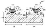
具体的には、図1は(断面図により)、絶縁領域108で隔てられたnFETデバイス領域104とpFETデバイス領域106とを含む半導体基板102を備えた半導体構造体100を示す。nFETデバイス領域104の上には、ゲート誘電体122と、n型ドーパントでドープされたゲート導体124とを含むnFET120がある。nFET120は、半導体基板102の内部に配置されたソース/ドレイン拡散領域126と、少なくともゲート導体124の露出側壁の上に配置されたスペーサ121とを含む。pFETデバイス領域106は、ゲート誘電体122と、p型ドーパントでドープされたゲート導体124とを含んだpFETを含む。pFET128のソース/ドレイン拡散領域126は、pFETの設置面積で半導体基板102の内部に存在し、スペーサ121はまた、少なくともゲート導体124の露出側壁の上に存在する。示されるように、引張り窒化物ライナ130はnFETデバイス領域104内に存在し、一方、圧縮窒化物ライナ132はpFETデバイス領域106内に存在する。
Specifically, FIG. 1 (through a cross-sectional view) shows a
この従来技術の例においては、応力ライナ(ライナ130及び132で表される)は、トランジスタ構造体に力を及ぼすストレッサ材料である。両方のストレッサの形態(この例においては、トランジスタ・チャネルに自己整合したライナ)、その応力の型(引張り又は圧縮)、及びトランジスタ構造体が、それぞれのトランジスタ・チャネル125の内部に有益な歪みを生じる。ひとたび、トランジスタの結晶型及び構造並びにストレッサが定まると、ストレッサ内の高レベルの応力がチャネル125内により大きな歪みを生じ、より高い性能向上がもたらされる。従って、ストレッサ材料内の応力レベルを上昇させることが非常に望ましい。
In this prior art example, the stress liner (represented by
他の型のストレッサ材料も従来技術において知られている。例えば、シリコン結晶内に埋め込まれたSiGe結晶アイランドは大きな圧縮応力を周囲のSi内に引き起こす。この結晶ストレッサを利用してSiベースのpFETの性能を向上させることができる。別の例では、アモルファス窒化シリコン・ストレッサがゲート・スペーサの形態に形作られる。 Other types of stressor materials are also known in the prior art. For example, SiGe crystal islands embedded in silicon crystals cause large compressive stresses in the surrounding Si. Using this crystal stressor, the performance of the Si-based pFET can be improved. In another example, an amorphous silicon nitride stressor is formed in the form of a gate spacer.
種々の型及び形態のストレッサの組合せもまた、デバイス性能をさらに向上させることが知られている。例えば、前記の埋め込まれたSiGe結晶ストレッサを前記のアモルファス応力ゲート・ライナと組み合わせてSiベースのpFETの性能をさらに改善することができる。 Combinations of various types and forms of stressors are also known to further improve device performance. For example, the embedded SiGe crystal stressor can be combined with the amorphous stress gate liner to further improve the performance of Si-based pFETs.
従来技術においてアモルファス応力ゲート・ライナを形成するための進歩はなされたが、引張り及び圧縮歪みの両方の場合に対する応力のレベルを高めるアモルファス・ストレッサ材料を供給する必要がある。そのような材料は、特定のストレッサ形態、半導体結晶の型、半導体デバイスの型、及びデバイスの構造に関わらず、隣接する半導体構造体に有益なレベルの歪みを増加させるために用いられることになる。 While progress has been made in the prior art to form amorphous stress gate liners, there is a need to provide amorphous stressor materials that increase the level of stress for both tensile and compressive strains. Such materials will be used to increase the level of strain beneficial to adjacent semiconductor structures, regardless of the particular stressor morphology, semiconductor crystal type, semiconductor device type, and device structure. .
さらに、改善されたストレッサ材料は、隣接するミクロ構造体の温度に敏感な要素を保護するために低温(凡そ400℃〜550℃又はそれ以下の程度の)で形成されることが望ましい。例えば、GaAsなどの特定のIII−V族化合物半導体は、500℃より高温では不安定である。さらに、シリコン・ベースのトランジスタの特定の要素(例えば、シリサイド・コンタクト及び高活性ドーパント)は高温処理によって有害な影響を受ける可能性がある。 Furthermore, it is desirable that the improved stressor material be formed at low temperatures (on the order of about 400 ° C. to 550 ° C. or less) to protect the temperature sensitive elements of adjacent microstructures. For example, certain III-V compound semiconductors such as GaAs are unstable at temperatures above 500 ° C. In addition, certain elements of silicon-based transistors (eg, silicide contacts and highly active dopants) can be adversely affected by high temperature processing.
プラズマ強化化学気相堆積(PECVD)プロセスは凡そ500℃より低温で実施される。アモルファス・ストレッサ材料の1つの周知の例は、PECVDプロセスによって堆積させたアモルファス窒化シリコン膜である。通常、PECVDによって形成された窒化シリコン膜内の応力は、最適化された気体流量、プラズマ出力及び他の堆積パラメータにより調節される。そのような最適化は、応力の符号(圧縮性又は引張り性)の調節には非常に効果的であるが、応力レベルには僅かな増加をもたらすだけである。 The plasma enhanced chemical vapor deposition (PECVD) process is performed at temperatures below approximately 500 ° C. One well-known example of an amorphous stressor material is an amorphous silicon nitride film deposited by a PECVD process. Typically, the stress in a silicon nitride film formed by PECVD is adjusted by optimized gas flow, plasma power, and other deposition parameters. Such optimization is very effective in adjusting the sign of stress (compressibility or tensile properties), but only slightly increases the stress level.
PECVD堆積温度を上昇させる(500℃を越えて)こと、又は、約600℃又はそれを越える温度で高温急速熱化学気相堆積(RTCVD)法を用いることによって、SiN薄膜内に比較的高い応力レベルを達成することも可能である。RTCVDは高歪み引張りSiN膜を作ることができるが、RTCVDプロセスの典型的な温度は700℃に近い。 Relatively high stress in the SiN thin film by increasing the PECVD deposition temperature (above 500 ° C.) or by using a high temperature rapid thermal chemical vapor deposition (RTCVD) process at a temperature of about 600 ° C. or above. It is also possible to achieve a level. RTCVD can produce high strain tensile SiN films, but the typical temperature of the RTCVD process is close to 700 ° C.
また、圧縮RTCVD膜が存在することは知られていない。最先端のCMOSデバイスは、比較的低い中間工程(middle−of−the−line、MOL)温度使用計画を有し、それが次第に約400℃の後工程(back−end−of−the−line、BEOL)温度に近づく。MOL温度使用計画の問題は、高温で不安定なNiSiをベースとするデバイスに対しては特に深刻になっているが、何故ならこれらのデバイス内の欠陥のレベルは450℃を越える温度により劇的に上昇するからである。従って、全ての高温MOLによる解決法は用いることができず、低温(450℃未満)でのPECVD法により高応力レベルを達成することが、65及び45nmノードのデバイス技術の重要な要素となっている。 Also, it is not known that a compressed RTCVD film exists. State-of-the-art CMOS devices have a relatively low middle-of-the-line (MOL) temperature usage scheme, which gradually increases to about 400 ° C. back-end-of-the-line, BEOL) approaches temperature. The problem of MOL temperature usage planning is particularly acute for NiSi-based devices that are unstable at high temperatures, because the level of defects in these devices is more dramatic with temperatures above 450 ° C. Because it rises to. Therefore, not all high temperature MOL solutions can be used, and achieving high stress levels by PECVD at low temperatures (below 450 ° C.) is an important element of 65 and 45 nm node device technology. Yes.
本発明は、アモルファス薄膜ストレッサの応力レベルを、そのストレッサの内部構造を修正することによって上昇させる方法を提供する。本発明の方法は、
基板の少なくとも表面の上に、アモルファス膜ストレッサ材料の第1の部分であって、第1の応力値を規定する機械的歪みの第1の状態を有する前記の第1の部分を形成するステップと、
アモルファス膜ストレッサ材料の第1の部分を、機械的歪みの第1の状態は実質的に変化させずに第1の応力値を増加させるように、高密度化するステップと
を含む。
本発明の方法において、用語「基板」は半導体基板及び/又はFETを含むことが意図されている。
The present invention provides a method for increasing the stress level of an amorphous thin film stressor by modifying the internal structure of the stressor. The method of the present invention comprises:
Forming a first portion of an amorphous film stressor material on at least a surface of the substrate, said first portion having a first state of mechanical strain defining a first stress value; ,
Densifying a first portion of the amorphous film stressor material such that the first stress value is increased without substantially changing the first state of mechanical strain.
In the method of the present invention, the term “substrate” is intended to include a semiconductor substrate and / or a FET.
幾つかの実施形態において、形成するステップ及び高密度化するステップは、アモルファス薄膜ストレッサ材料に対して予め選択された所望の厚さを得るまで何回でも繰り返される。
上記の本発明の方法により形成されるストレッサ膜は、随意に、表面高密度化の後に、その機械的歪みを変える(増加させる)既知の方法の1つで処理してさらにその応力を増加させることができる。ストレッサはまた、随意に、リソグラフィ及びエッチングにより、有用なミクロ構造体への効果を最大にするように任意の形態に成形することができる。
In some embodiments, the forming and densifying steps are repeated any number of times until a desired preselected thickness for the amorphous thin film stressor material is obtained.
The stressor film formed by the above-described method of the present invention is optionally treated with one of the known methods to change (increase) its mechanical strain after surface densification to further increase its stress. be able to. The stressor can also optionally be shaped into any form by lithography and etching to maximize the effect on useful microstructures.
本発明の1つの実施形態においては、アモルファス・ストレッサは、従来の堆積法で形成される水素含有アモルファス窒化シリコン(SiN)膜である。堆積後、水素含有アモルファスSiN膜は、低温プラズマ処理を用いて実施される高密度化プロセスを受けるが、その際、低温プラズマ処理はSiN膜の上部領域内に活性窒素(例えば、原子状窒素、分子状窒素、又は原子窒素イオンなど)を導入することによってSiN膜の上部領域の密度を高める。この実施形態において、プラズマ処理は約550℃又はそれ以下の温度で実施される。 In one embodiment of the invention, the amorphous stressor is a hydrogen-containing amorphous silicon nitride (SiN) film formed by conventional deposition methods. After deposition, the hydrogen-containing amorphous SiN film undergoes a densification process performed using low temperature plasma treatment, where the low temperature plasma treatment is activated nitrogen (eg, atomic nitrogen, The density of the upper region of the SiN film is increased by introducing molecular nitrogen or atomic nitrogen ions). In this embodiment, the plasma treatment is performed at a temperature of about 550 ° C. or lower.
本発明の方法は、ストレッサの内部応力を高める他の既知の方法と組み合わせて用いることができ、また有用なマイクロデバイスの電気的及び光学的パラメータを改善するように、そのストレッサを賢明に布設する種々の幾何学的スキームで用いることができる。本発明の方法はさらに、約550℃又はそれ以下の低い処理温度で機能するので、本発明の方法は温度に敏感なミクロ構造体に対して特に有用である。 The method of the present invention can be used in combination with other known methods of increasing the stressor's internal stress and wisely lays the stressor so as to improve the electrical and optical parameters of a useful microdevice. It can be used in various geometric schemes. Since the method of the present invention further functions at low processing temperatures of about 550 ° C. or lower, the method of the present invention is particularly useful for temperature sensitive microstructures.
薄膜の応力レベルを上昇させるのに用いられる他の既知の後処理は、処理される膜内の機械的な歪みの状態を、実質的にその化学結合を再配置することによって変化させることに向けられる。従って、そのような方法は1つの型の応力だけ(引張り又は圧縮)を増加させるように機能する。例えば、応力窒化シリコン膜の強熱は、その膜内に存在するSi−H及びN−H結合からの水素原子の切離し又は除去をもたらし、その結果引張り応力のレベルは上昇するが、圧縮応力のレベルは低下する。本発明は、引張り及び圧縮膜の両方に対して等しく効果的に機能するので、そのような従来技術からの脱却法を教示する。 Other known post treatments used to increase the stress level of a thin film are directed towards changing the state of mechanical strain in the processed membrane substantially by rearranging its chemical bonds. It is done. Thus, such a method functions to increase only one type of stress (tensile or compressive). For example, the intense heat of a stressed silicon nitride film results in the dissociation or removal of hydrogen atoms from Si-H and N-H bonds present in the film, resulting in an increase in the level of tensile stress but the compressive stress. The level drops. The present invention teaches a method of departure from such prior art as it works equally effectively for both tension and compression membranes.
本発明の方法は、堆積膜の応力を増加させながら、堆積膜の機械的歪み状態を保つことに向けられるので、従来技術から脱却するものである。従って、本発明の方法は、堆積時の膜内の歪みの符号及びレベルを独立に最適化すること、並びに結果の膜内の最終的な応力レベルを最適化することを可能にする。 Since the method of the present invention is directed to maintaining the mechanical strain state of the deposited film while increasing the stress of the deposited film, it is a departure from the prior art. Thus, the method of the present invention makes it possible to independently optimize the sign and level of strain in the film during deposition and to optimize the final stress level in the resulting film.
本発明は、アモルファス薄膜ストレッサ材料に対する応力のレベルを、膜の内部構造を修正する技法によって上昇させる方法を提供するものであるが、以下の議論及び本願に添付の図面を参照しながら、以下に詳細に説明される。本願の図面は例証のために与えられるもので、一定の尺度で描かれてはいないことに注意されたい。 The present invention provides a method of increasing the level of stress on an amorphous thin film stressor material by a technique that modifies the internal structure of the film, with the following discussion and with reference to the drawings attached hereto. It will be explained in detail. It should be noted that the drawings in this application are provided for purposes of illustration and are not drawn to scale.
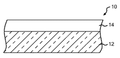
本発明の基本的な加工処理ステップを示す図2〜図4を参照する。具体的には、図2は、半導体基板12の表面上に形成されたアモルファス薄膜ストレッサ材料14を含む構造体10を示す。図2〜図4は半導体基板12の小さな部分だけを示すこと、及び、本発明の方法は図5に示されるようなトランジスタ・デバイスを上部に含む半導体基板12の全表面にわたって用いることができることに注意されたい。図5に示される構造体は以下で詳細に説明される。以下の議論はストレッサ材料を半導体基板上に堆積させる状況を説明するが、本発明は、ストレッサ材料がFETの上に、又はFET及び半導体基板の両方の上に形成されるときにも同様に良好に機能する。
Reference is made to FIGS. 2-4 showing the basic processing steps of the present invention. Specifically, FIG. 2 shows a
図2を再び参照すると、構造体は初めに半導体基板12を準備することで作成される。半導体基板12は、表面上に配置された1つ又は複数のトランジスタを有する前加工された基板とすることができる。明瞭さのためにトランジスタは図2〜図4の断面図には示されていない。本発明で用いられる半導体基板12は、例えば、Si、SiGe、SiGeC、SiC、GaAs、InAs、InP及び他のIII/V族及びII/VI族化合物半導体を含んだ任意の半導体材料を含む。半導体基板12はまた、例えば、Si/SiGe、シリコン・オン・インシュレータ(SOI)又はSiGe・オン・インシュレータ基板などの層状半導体基板を含むことができる。半導体基板12はまた、ドープ型又は非ドープ型とするか、或いは1つ若しくは複数のドープ領域を有することができる。例えば、半導体基板12は、ウェル領域、ソース/ドレイン拡散領域、ソース/ドレイン延長領域、ハロ領域などを有することができる。半導体基板12はまた、種々の型の半導体デバイスを互いに絶縁する絶縁領域を含むことができる。半導体基板12は、例えば、(110)、(100)、又は(111)を含む主要な又は副次的な結晶方位を有することができる。半導体基板12は、無歪み型又は歪み型とするか、或いは歪み領域と無歪み領域の組み合わせを有することができる。
Referring back to FIG. 2, the structure is created by first preparing the
半導体基板12は、同じ又は異なる半導体材料からなる少なくとも2つの平面領域を含む複合半導体基板とすることができるが、ここで各々の領域は、「複合結晶方位基板上の高性能CMOS SOIデバイス」と題する同一出願人に譲渡された同時係属中の特許文献1において作成されるように異なる結晶方位を有する。
The
半導体基板12を準備した後、アモルファス薄膜ストレッサ材料14が半導体基板12の少なくとも表面上に形成される。本発明によれば、本発明のアモルファス薄膜ストレッサ材料14は、第1の応力値を規定する機械的歪み(圧縮又は引張りの)の第1の状態を有する。第1の応力値は、堆積させる材料、上部に材料が形成される基板、そしてその膜の堆積に用いた方法によって変化し得る。PECVD法による堆積時の引張り歪み下にあるアモルファス水素含有SiN膜に対する典型的な第1の応力値は凡そ0.5〜1.0GPaであり、一方圧縮歪み下にある同じ膜の典型的な第1の応力値は凡そ1〜1.5GPaである。
After preparing the
アモルファス薄膜ストレッサ材料14(堆積時の膜と呼ぶことができる)は、例えば、化学気相堆積、プラズマ強化化学気相堆積又は急速熱化学気相堆積を含む従来の堆積プロセスを利用して形成される。典型的には、堆積プロセスは、半導体基板12の内部又はその上に配置された温度に敏感なあらゆる要素に悪影響を与えないように、約550℃又はそれ以下の温度で実施される。アモルファス薄膜ストレッサ材料14はプラズマ強化化学気相堆積プロセスで形成されることが好ましい。
本発明のこの時点で形成された堆積時のアモルファス薄膜ストレッサ材料14は、典型的には凡そ1nmから200nmまでの厚さを有し、約20nmから約100nmまでの厚さがより典型的である
Amorphous thin film stressor material 14 (which can be referred to as a film during deposition) is formed utilizing conventional deposition processes including, for example, chemical vapor deposition, plasma enhanced chemical vapor deposition, or rapid thermal chemical vapor deposition. The Typically, the deposition process is performed at a temperature of about 550 ° C. or lower so as not to adversely affect any temperature sensitive elements disposed within or on the
The deposited amorphous thin film stressor material 14 formed at this point of the present invention typically has a thickness of about 1 nm to 200 nm, with a thickness of about 20 nm to about 100 nm being more typical.
アモルファス薄膜ストレッサ材料14は、例えば、窒化物、酸化物又は金属を含む任意の応力誘起材料を含む。アモルファス・ストレッサ材料14はSiNから成ることが好ましい。応力誘起材料は水素を含むことができ、従ってここでは、水素含有SiNのような水素含有材料が完成される。用語「アモルファス」は本明細書では、ストレッサ材料14が明確な結晶構造をもたないことを表すのに用いられる。 The amorphous thin film stressor material 14 includes any stress inducing material including, for example, nitrides, oxides or metals. The amorphous stressor material 14 is preferably composed of SiN. The stress-inducing material can include hydrogen, thus completing a hydrogen-containing material such as hydrogen-containing SiN here. The term “amorphous” is used herein to indicate that the stressor material 14 does not have a well-defined crystal structure.
図2に示される堆積時のアモルファス薄膜ストレッサ材料14は、本発明のこの時点では従来技術のストレッサ材料と変わらない。図3は、堆積時のストレッサ材料14を含む構造体に高密度化ステップを施した後に形成される構造体を示す。本発明によれば、高密度化ステップは、ストレッサ材料の機械的歪みの第1の状態は実質的に変化させずに第1の応力値を増加させるような条件下で実施される。即ち、本発明の高密度化ステップは、ストレッサ材料14の応力値を第1の応力値より大きな値に増加させ、一方、その層が圧縮歪み下にあるか又は引張り歪み下にあるかを変更しない。例証として、本発明の高密度化ステップは、引張り歪み水素含有SiN材料の応力値を堆積時の値約0.8GPaから第2の応力値約1.2GPaまで増加させ、同時に圧縮歪み材料の応力値もまた堆積時の値約1.4GPaから第2の応力値約2.0GPaまで増加させる。 The deposited amorphous thin film stressor material 14 shown in FIG. 2 is no different from the prior art stressor material at this point of the invention. FIG. 3 shows the structure formed after applying a densification step to the structure containing the stressor material 14 during deposition. According to the present invention, the densification step is performed under conditions that increase the first stress value without substantially changing the first state of mechanical strain of the stressor material. That is, the densification step of the present invention increases the stress value of the stressor material 14 to a value greater than the first stress value, while changing whether the layer is under compressive strain or tensile strain. do not do. Illustratively, the densification step of the present invention increases the stress value of a tensile strain hydrogen-containing SiN material from a deposition value of about 0.8 GPa to a second stress value of about 1.2 GPa, while simultaneously reducing the stress of the compressive strain material. The value is also increased from a deposition value of about 1.4 GPa to a second stress value of about 2.0 GPa.
図3に示されるように、高密度化ステップは、上部領域20と下部領域18を有するアモルファス薄膜ストレッサ材料16を生ずる。上部領域20は、下部領域18よりも大きな密度を有し、下部領域18の密度は典型的には堆積時の膜14の密度である。上部及び下部領域内の密度は、例えば、ストレッサ材料の型及び厚さ、並びに高密度化ステップの条件を含む多くの因子によって変化し得る。典型的には、そして上に例示されたストレッサ材料に対しては、水素含有SiNストレッサ膜の下部領域18は約2.4gm/ccの密度をもち、一方、同じ膜の上部領域20は約2.6gm/ccの密度をもつ。
As shown in FIG. 3, the densification step results in an amorphous thin
本発明の高密度化ステップにより形成されたアモルファス薄膜ストレッサ材料16の上部領域20の厚さは、用いられる高密度化プロセスの型及び高密度化中に用いられた条件によって変化し得る。典型的には、高密度化により形成される上部領域20の厚さは、約0.5nm(好ましくは約1.0nm)から約50nm(好ましくは約20nm)までであり、約1nmから約10nmまでの厚さがより典型的である。
The thickness of the
堆積時のアモルファス薄膜ストレッサ材料14の高密度化は、その層の表面部分の密度を増加させることのできる任意の技法を用いて実施することができる。堆積時の薄膜ストレッサ材料14の応力値を増加させるのに利用できる高密度化プロセスには、約500℃若しくはそれ以下の温度で実施されるプラズマ窒化又は放射照射が含まれるが、それらに限定はされない。本発明における高密度化はプラズマ窒化プロセスを用いて達成することが好ましい。 Densification of amorphous thin film stressor material 14 during deposition can be performed using any technique that can increase the density of the surface portion of the layer. Densification processes that can be used to increase the stress value of the thin film stressor material 14 during deposition include, but are not limited to, plasma nitridation or radiation performed at a temperature of about 500 ° C. or lower. Not. Densification in the present invention is preferably achieved using a plasma nitridation process.
堆積時のアモルファス薄膜ストレッサ材料14の上部部分を高密度化するためにプラズマ窒化を用いるときには、原子状窒素、分子状窒素、原子窒素イオン又はこれらの組合せを含む任意の窒素含有プラズマを用いることができる。窒素含有プラズマは、例えば、N2、NO、NH3、N2O又はこれらの混合物などの任意の窒素含有源から誘導される。前述のように、本発明で用いられるプラズマ窒化プロセスは、約550℃又はそれ以下の温度で実施され、約350℃から約450℃までの温度がより典型的である。プラズマ窒化プロセスは、典型的には約0.5秒から約200秒までの時間実施され、約5秒から約60秒までの時間がより典型的である。時間範囲をここで述べた範囲より延長しても応力レベルをさらに改善することはできないことに注意されたい。
When using plasma nitridation to densify the upper portion of the amorphous thin film stressor material 14 during deposition, any nitrogen-containing plasma including atomic nitrogen, molecular nitrogen, atomic nitrogen ions, or combinations thereof may be used. it can. Nitrogen-containing plasma, for example,
本発明のこの時点において、高密度化されたアモルファス薄膜ストレッサ材料16は、堆積時の膜に比べて大きな応力値を有するが、有用なミクロ構造体への効果(即ち、力を及ぼすこと)を最大にするために、例えばスペーサ又はライナなどの任意の形態に成形することができる。成形はリソグラフィ及びエッチングによって達成することができる。
At this point of the invention, the densified amorphous thin
幾つかの実施形態においては、図4に示されるように、堆積及び高密度化のステップは、非高密度化及び高密度化領域の交互の層を有する多層アモルファス薄膜ストレッサ材料を設けるために何回でも繰り返すことができる。さらに、本発明のステップは、増加した応力値を有し予め設定した厚さを有するストレッサ材料を設けるために何回でも繰り返すことができる。図4においては、構造体は、それぞれが下部の非高密度化領域(18、18A及び18B)及び上部の高密度化領域(20、20A及び20B)を有する、3層の高密度化薄膜ストレッサ材料(16、16A及び16B)を含む。 In some embodiments, as shown in FIG. 4, the deposition and densification steps are performed to provide a multilayer amorphous thin film stressor material having alternating layers of non-densified and densified regions. Can be repeated any number of times. Furthermore, the steps of the present invention can be repeated any number of times to provide a stressor material having an increased stress value and a preset thickness. In FIG. 4, the structure is a three-layer densified thin film stressor, each having a lower non-densified region (18, 18A and 18B) and an upper densified region (20, 20A and 20B). Material (16, 16A and 16B).
図4に示される多層アモルファス薄膜ストレッサ材料は、有用なミクロ構造体への効果(即ち、力を及ぼすこと)を最大にするために、例えばスペーサ又はライナなどの任意の形態に成形することができる。また、多層高密度化アモルファス薄膜ストレッサ材料は、随意に、材料の応力値をさらに増加させることのできる任意の従来の方法で処理することができる。 The multilayer amorphous thin film stressor material shown in FIG. 4 can be formed into any form, such as a spacer or liner, to maximize the useful microstructure effect (ie, exerting force). . Also, the multilayer densified amorphous thin film stressor material can optionally be processed in any conventional manner that can further increase the stress value of the material.
本発明の種々のステップは、堆積ステップと高密度化ステップの間で真空を破ることなくイン・サイチュ(in−situ)で実施することができるが、或いは、真空は堆積ステップと高密度化ステップの間で又は多重の堆積及び高密度化ステップの間で破ることができる。 The various steps of the present invention can be performed in-situ without breaking the vacuum between the deposition step and the densification step, or the vacuum can be performed in the deposition and densification steps. Or between multiple deposition and densification steps.
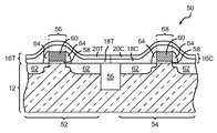
前述のように、本発明の方法は、上部に形成されたトランジスタを含む半導体基板の上に形成される応力ライナ材料の応力値を増加させるために用いることができる。そのような構造体は、例えば図5に示される。図5は、下部の非高密度化領域18及び上部の高密度化領域20を含む本発明の高密度化アモルファス薄膜ストレッサ材料16の存在を除いて、図1に類似していることに注意されたい。
As mentioned above, the method of the present invention can be used to increase the stress value of a stress liner material formed on a semiconductor substrate that includes a transistor formed thereon. Such a structure is shown, for example, in FIG. Note that FIG. 5 is similar to FIG. 1 except for the presence of the densified amorphous thin
具体的には、図5は(断面図により)、絶縁領域56で隔てられたnFETデバイス領域52とpFETデバイス領域54を有する半導体基板12を備えた半導体構造体50を示す。nFETデバイス領域52の上には、ゲート誘電体58、及びn型ドーパントでドープされたゲート導体60を含むnFET66がある。nFET66はまた、半導体基板12の内部に配置されたソース/ドレイン拡散領域62と、少なくともゲート導体60の露出側壁上に配置されたスペーサ64とを含む。pFETデバイス領域54は、ゲート誘電体58、及びp型ドーパントでドープされたゲート導体60を含んだpFETを含む。pFET68のソース/ドレイン拡散領域62は、pFET68の設置面積で半導体基板12の内部に存在し、スペーサ64はまた、少なくともゲート導体60の露出側壁上に存在する。示されるように、領域18T及び20Tを含む引張り窒化物ライナ16Tは、nFETデバイス領域52の内部に存在し、一方、領域18C及び20Cを含む圧縮窒化物ライナ16CはpFETデバイス領域54の内部に存在する。
Specifically, FIG. 5 (through a cross-sectional view) shows a
図5に示される構造体は、本発明の負のストレッサ材料が下部領域よりも高い密度をもつ上部領域を有するが、当技術分野で周知の従来の方法を用いて形成される。例えば、絶縁領域56は、初めにリソグラフィ及びエッチングにより基板内にトレンチを画定することによって形成することができる。エッチング・ステップに続いて、随意のトレンチ誘電体ライナを形成することができ、その後に酸化物などのトレンチ誘電体をトレンチ内に堆積させることができる。トレンチ充填の後で化学機械研磨(CMP)又は研削などの平坦化プロセスを実施することができる。或いは、シリコンの位置選定酸化プロセスを用いて絶縁領域を形成することができる。
The structure shown in FIG. 5 is formed using conventional methods well known in the art, although the negative stressor material of the present invention has an upper region with a higher density than the lower region. For example, the insulating
次に、任意の従来のCMOSプロセスを利用して、FETが半導体基板12の表面上に形成され、nFETデバイス領域52及びpFETデバイス領域54が形成される。1つの方法は、ゲート誘電体及びゲート導体を含む層状スタックを半導体基板12の表面上に形成するステップを含む。ゲート誘電体は、酸化などの熱処理又は従来の堆積法によって形成することができる。本発明において用いることのできるゲート誘電体は、酸化物、窒化物、酸窒化物又はそれらの多層を含む。ゲート導体は従来の堆積法によって形成される。ポリSi又はSiGeゲートが用いられるときは、導電性材料はイン・サイチュのドーピング堆積プロセスにより、又は堆積及びその後のイオン注入により形成することができる。注入マスク及び異なるイオン注入を用いて異なる導電率のFETを形成することができる。層状スタックの形成に続いて、少なくともゲート導体(及び隋意にゲート誘電体)をリソグラフィ及びエッチングによりパターン付けする。熱処理を用いて各パターン付けされたゲート領域の周りに保護層を形成することができる。その後、ソース/ドレイン延長部がイオン注入及びアニール処理により形成される。次に側壁スペーサが堆積及びエッチングにより形成され、その後にソース/ドレイン拡散領域がイオン注入及びアニール処理により形成される。上記のS/D延長部を活性化するのに用いられるアニール処理ステップは省くことができ、活性化はソース/ドレイン領域の活性化中に起り得る。幾つかの実施形態においては、側壁スペーサは、本発明の高密度化アモルファス・ストレッサ材料だけを又は別の絶縁材料とともに含むことができる。
この方法に加えて、従来のゲート置き換えプロセスを用いて半導体基板の表面上にFETを形成することができる。
Next, using any conventional CMOS process, an FET is formed on the surface of the
In addition to this method, FETs can be formed on the surface of a semiconductor substrate using a conventional gate replacement process.
次に、本発明のストレッサ材料が前述のステップを用いて形成される。具体的には、各々のFETの上のストレッサ材料は、本発明のステップを用いて単一プロセスで加工処理することができる。代替的に、各々のFET上のストレッサ材料は、多重ステップで加工処理されるが、その際、非保護領域内のストレッサ材料の形成中、1つのデバイス領域上にブロック・マスクが形成され、次いでブロック・マスクが除去され、そして本発明のストレッサ材料を含有する先の非保護領域の上にブロック・マスクを形成することによってプロセスが繰り返される。高密度化後に、エッチング・ステップを用いてストレッサ材料を任意の所望の形状に成形することができる。 The stressor material of the present invention is then formed using the steps described above. Specifically, the stressor material on each FET can be processed in a single process using the steps of the present invention. Alternatively, the stressor material on each FET is processed in multiple steps, where a block mask is formed on one device area during the formation of the stressor material in the unprotected area, and then The block mask is removed and the process is repeated by forming a block mask over the previous unprotected area containing the stressor material of the present invention. After densification, an etching step can be used to shape the stressor material into any desired shape.
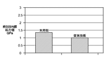
図6及び図7は、引張り歪み下(図6)及び圧縮歪み下(図7)での本発明の多層高密度化アモルファスSiNストレッサ材料を、多層中断堆積させた従来技術の薄膜SiNストレッサ材料と比較したグラフである。本発明の材料は「本発明」と標識付けし、従来技術の材料は「従来技術」と標識付けしている。種々のSiN層の中断堆積法による従来技術のSiN膜形成方法は、ストレッサ材料の応力値を増加させる既知の手段を与える。これらの図に示されるデータは、本発明の方法はSiNの応力値を、従来技術を用いて達成できる値を超えて、さらに増加させることができることを示す。
具体的には、本発明のプロセスを用いると、各堆積ステップの間に高密度化を施さない類似の多層膜に比べて、応力値の70%の増加を達成することができる。
FIGS. 6 and 7 show prior art thin film SiN stressor materials in which the multilayer densified amorphous SiN stressor material of the present invention under tensile strain (FIG. 6) and compressive strain (FIG. 7) is multilayered and deposited intermittently. It is the graph compared. The material of the present invention is labeled “Invention” and the prior art material is labeled “Prior Art”. Prior art SiN film formation methods by interrupted deposition of various SiN layers provide a known means of increasing the stress value of the stressor material. The data shown in these figures shows that the method of the present invention can further increase the stress value of SiN beyond what can be achieved using the prior art.
Specifically, using the process of the present invention, a 70% increase in stress value can be achieved compared to similar multilayer films that do not undergo densification during each deposition step.
PECVDを利用する本発明の方法を用いて、16層の応力SiN膜を調製した。この多層構造体の各SiN層は、10〜10,000Åの間の厚さをもち、各々の堆積の間に
SiN膜に活性窒素処理、即ちプラズマ窒化を用いて高密度化を施した。その膜のX線反射率(XRR)データは、各々の個々の層が2つの領域(下部領域、及び下部領域よりも高い密度を有する上部領域)から成ることを示した。以下の表1は、上部領域の密度をまとめたものである。明らかに活性窒素処理は実質的に高密度の上部膜をもたらす。上部領域の厚さは15〜25Åの間と見積られる。処理の最適の継続時間は10秒から60秒までである。この時間範囲を超えて処理時間を長くしても、上部領域の密度には何ら実質的な増加は生じず、膜の厚さ又は応力値を増加させることもなかった。
A 16-layer stress SiN film was prepared using the method of the present invention utilizing PECVD. Each SiN layer of this multilayer structure had a thickness of 10 to 10,000 mm, and the SiN film was densified using active nitrogen treatment, that is, plasma nitridation, during each deposition. X-ray reflectivity (XRR) data for the film indicated that each individual layer consisted of two regions (a lower region and an upper region having a higher density than the lower region). Table 1 below summarizes the density of the upper region. Clearly, the active nitrogen treatment results in a substantially dense upper film. The thickness of the upper region is estimated to be between 15 and 25 mm. The optimum duration of processing is from 10 to 60 seconds. Increasing the processing time beyond this time range did not cause any substantial increase in the density of the upper region, nor did it increase the film thickness or stress value.

本発明は、その好ましい実施形態に関して詳しく示され説明されているが、当業者であれば、本発明の趣旨と範囲から逸脱することなく形態及び細部における前述の及び他の変更を施すことができることを理解するであろう。従って、本発明は説明され例証された通りの形態及び細部に限定されず、添付の特許請求の範囲に含まれることが意図されている。 Although the present invention has been particularly shown and described with respect to preferred embodiments thereof, those skilled in the art can make the foregoing and other changes in form and detail without departing from the spirit and scope of the invention. Will understand. Accordingly, the invention is not limited to the precise forms and details described and illustrated, but is intended to be encompassed by the following claims.
本発明は半導体デバイスの製造のために有用である。より具体的には、本発明はアモルファス薄膜ストレッサ内の応力の増加したレベルを提供する。この応力誘起材料により提供される半導体デバイスは、CMOS回路に対して非常に重要な著しく優れた性能を有する。 The present invention is useful for the manufacture of semiconductor devices. More specifically, the present invention provides increased levels of stress in amorphous thin film stressors. The semiconductor device provided by this stress-inducing material has significantly superior performance that is very important for CMOS circuits.
10:構造体
12:半導体基板
14、16、16A、16B:アモルファス薄膜ストレッサ材料
18、18A、18B:下部領域(非高密度化領域)
20、20A、20B:上部領域(高密度化領域)
50、100:半導体構造体
102:半導体領域
52、104:nFETデバイス領域
54、106:pFETデバイス領域
56、108:絶縁領域
66、120:nFET
68,128:pFET
64、121:スペーサ
58、122:ゲート誘電体
60、124:ゲート導体
125:トランジスタ・チャネル
62、126:ソース/ドレイン拡散領域
16T、130:引張り窒化物ライナ
16C、132:圧縮窒化物ライナ
10: Structure 12:
20, 20A, 20B: upper region (high density region)
50, 100: Semiconductor structure 102:
68, 128: pFET
64, 121:
Claims (16)
基板の少なくとも表面上にアモルファス膜ストレッサ材料を形成するステップと、
前記アモルファス膜ストレッサ材料の機械的歪みの状態は実質的に変化させずに当該ストレッサ材料の応力値を増加させるために、前記アモルファス膜ストレッサ材料の上部領域が下部領域に比べてより高い密度を有するように高密度化するステップであって、前記機械的歪みの前記状態は引張り状態又は圧縮状態のいずれか一方である、前記高密度化するステップと
を含む、前記方法。A method for increasing the stress level of a deposited stressor material, comprising:
Forming an amorphous film stressor material on at least a surface of the substrate;
In order to increase the stress value of the stressor material without substantially changing the mechanical strain state of the amorphous film stressor material, the upper region of the amorphous film stressor material has a higher density than the lower region. And densifying, wherein the state of the mechanical strain is either a tensile state or a compressed state .
基板の少なくとも表面上にプラズマ強化化学気相堆積によってアモルファス膜ストレッサ材料を形成するステップと、
前記アモルファス膜ストレッサ材料の機械的歪みの状態は実質的に変化させずに当該ストレッサ材料の応力値を増加させるために、550℃又はそれ以下の温度におけるプラズマ窒化により、前記アモルファス膜ストレッサ材料の上部領域が下部領域に比べてより高い密度を有するように高密度化するステップであって、前記機械的歪みの前記状態は引張り状態又は圧縮状態のいずれか一方である、前記高密度化するステップと
を含む、前記方法。A method of increasing the stress level of a stressor material during deposition,
Forming an amorphous film stressor material by plasma enhanced chemical vapor deposition on at least the surface of the substrate;
In order to increase the stress value of the stressor material without substantially changing the state of mechanical strain of the amorphous film stressor material, plasma nitridation at a temperature of 550 ° C. or lower is used to increase the stress of the amorphous film stressor material. Densifying so that the region has a higher density than the lower region, wherein the state of the mechanical strain is either a tensile state or a compressed state; and Said method.
絶縁領域によって隔てられた、少なくとも1つのnFETを含む少なくとも1つのnFET領域と、少なくとも1つのpFETを含む少なくとも1つのpFET領域とを含む半導体基板を準備するステップと、
前記基板の少なくとも表面上並びに前記nFET及びpFETの上に、アモルファス膜ストレッサ材料を形成するステップと、
前記アモルファス膜ストレッサ材料の機械的歪みの状態は実質的に変化させずに当該ストレッサ材料の応力値を増加させるために、前記アモルファス膜ストレッサ材料の上部領域が下部領域に比べてより高い密度を有するように高密度化するステップであって、前記機械的歪みの前記状態は引張り状態又は圧縮状態のいずれか一方である、前記高密度化するステップと
を含む、前記方法。A method of forming a semiconductor structure, comprising:
Providing a semiconductor substrate including at least one nFET region including at least one nFET and at least one pFET region including at least one pFET separated by an insulating region;
Forming an amorphous film stressor material on at least a surface of the substrate and on the nFET and pFET;
The upper region of the amorphous film stressor material has a higher density than the lower region in order to increase the stress value of the stressor material without substantially changing the state of mechanical strain of the amorphous film stressor material. And densifying, wherein the state of the mechanical strain is either a tensile state or a compressed state .
Applications Claiming Priority (3)
| Application Number | Priority Date | Filing Date | Title |
|---|---|---|---|
| US10/907,454 | 2005-04-01 | ||
| US10/907,454 US7585704B2 (en) | 2005-04-01 | 2005-04-01 | Method of producing highly strained PECVD silicon nitride thin films at low temperature |
| PCT/US2006/011391 WO2006107669A2 (en) | 2005-04-01 | 2006-03-29 | Method of producing highly strained pecvd silicon nitride thin films at low temperature |
Publications (3)
| Publication Number | Publication Date |
|---|---|
| JP2008538257A JP2008538257A (en) | 2008-10-16 |
| JP2008538257A5 JP2008538257A5 (en) | 2009-02-19 |
| JP4818352B2 true JP4818352B2 (en) | 2011-11-16 |
Family
ID=37071113
Family Applications (1)
| Application Number | Title | Priority Date | Filing Date |
|---|---|---|---|
| JP2008504277A Expired - Fee Related JP4818352B2 (en) | 2005-04-01 | 2006-03-29 | Method for increasing the stress level of a deposited stressor material and method for forming a semiconductor structure |
Country Status (6)
| Country | Link |
|---|---|
| US (1) | US7585704B2 (en) |
| EP (1) | EP1864319A4 (en) |
| JP (1) | JP4818352B2 (en) |
| CN (1) | CN101584025B (en) |
| TW (1) | TWI391516B (en) |
| WO (1) | WO2006107669A2 (en) |
Families Citing this family (53)
| Publication number | Priority date | Publication date | Assignee | Title |
|---|---|---|---|---|
| US9257302B1 (en) | 2004-03-25 | 2016-02-09 | Novellus Systems, Inc. | CVD flowable gap fill |
| US7524735B1 (en) | 2004-03-25 | 2009-04-28 | Novellus Systems, Inc | Flowable film dielectric gap fill process |
| US7582555B1 (en) * | 2005-12-29 | 2009-09-01 | Novellus Systems, Inc. | CVD flowable gap fill |
| TWI259534B (en) * | 2005-05-20 | 2006-08-01 | Ind Tech Res Inst | Method for fabricating semiconductor device |
| US7566655B2 (en) * | 2005-05-26 | 2009-07-28 | Applied Materials, Inc. | Integration process for fabricating stressed transistor structure |
| US8129290B2 (en) * | 2005-05-26 | 2012-03-06 | Applied Materials, Inc. | Method to increase tensile stress of silicon nitride films using a post PECVD deposition UV cure |
| US8138104B2 (en) * | 2005-05-26 | 2012-03-20 | Applied Materials, Inc. | Method to increase silicon nitride tensile stress using nitrogen plasma in-situ treatment and ex-situ UV cure |
| US20070105292A1 (en) * | 2005-11-07 | 2007-05-10 | Neng-Kuo Chen | Method for fabricating high tensile stress film and strained-silicon transistors |
| US8936702B2 (en) * | 2006-03-07 | 2015-01-20 | Micron Technology, Inc. | System and method for sputtering a tensile silicon nitride film |
| US7560318B2 (en) * | 2006-03-13 | 2009-07-14 | Freescale Semiconductor, Inc. | Process for forming an electronic device including semiconductor layers having different stresses |
| JP2007324391A (en) * | 2006-06-01 | 2007-12-13 | Matsushita Electric Ind Co Ltd | Semiconductor device and its manufacturing method |
| US20070298623A1 (en) * | 2006-06-26 | 2007-12-27 | Spencer Gregory S | Method for straining a semiconductor device |
| US7479465B2 (en) | 2006-07-28 | 2009-01-20 | Freescale Semiconductor, Inc. | Transfer of stress to a layer |
| US20080083955A1 (en) * | 2006-10-04 | 2008-04-10 | Kanarsky Thomas S | Intrinsically stressed liner and fabrication methods thereof |
| US9825802B2 (en) | 2006-10-31 | 2017-11-21 | Telecom Italia S.P.A. | Management of seamless handover between different communication systems in an IP dual-mode terminal |
| US9245739B2 (en) | 2006-11-01 | 2016-01-26 | Lam Research Corporation | Low-K oxide deposition by hydrolysis and condensation |
| US7700499B2 (en) * | 2007-01-19 | 2010-04-20 | Freescale Semiconductor, Inc. | Multilayer silicon nitride deposition for a semiconductor device |
| DE102007004824A1 (en) * | 2007-01-31 | 2008-08-07 | Advanced Micro Devices, Inc., Sunnyvale | Improved stress transfer in an interlayer dielectric by using an additional stress layer over a dual strain layer in a semiconductor device |
| US7608522B2 (en) * | 2007-03-11 | 2009-10-27 | United Microelectronics Corp. | Method for fabricating a hybrid orientation substrate |
| US20080237658A1 (en) * | 2007-03-26 | 2008-10-02 | United Microelectronics Corp. | Semiconductor device and method of fabricating the same |
| JP2008282901A (en) | 2007-05-09 | 2008-11-20 | Sony Corp | Semiconductor device, and manufacturing method of semiconductor device |
| US8440580B2 (en) * | 2007-09-11 | 2013-05-14 | United Microelectronics Corp. | Method of fabricating silicon nitride gap-filling layer |
| DE102007052051B4 (en) * | 2007-10-31 | 2012-09-20 | Advanced Micro Devices, Inc. | Fabrication of stress-inducing layers over a device region with dense transistor elements |
| US7863646B2 (en) * | 2007-12-13 | 2011-01-04 | International Business Machines Corporation | Dual oxide stress liner |
| US20090152639A1 (en) * | 2007-12-18 | 2009-06-18 | Texas Instruments Incorporated | Laminated Stress Overlayer Using In-SITU Multiple Plasma Treatments for Transistor Improvement |
| DE102007063272B4 (en) * | 2007-12-31 | 2012-08-30 | Globalfoundries Inc. | Dielectric interlayer material in a strained layer semiconductor device with an intermediate buffer material |
| DE102007063230B4 (en) * | 2007-12-31 | 2013-06-06 | Advanced Micro Devices, Inc. | Semiconductor device with strained material layers and contact element and method of production thereof |
| US8557712B1 (en) | 2008-12-15 | 2013-10-15 | Novellus Systems, Inc. | PECVD flowable dielectric gap fill |
| US8278224B1 (en) | 2009-09-24 | 2012-10-02 | Novellus Systems, Inc. | Flowable oxide deposition using rapid delivery of process gases |
| KR101758944B1 (en) * | 2009-12-09 | 2017-07-18 | 노벨러스 시스템즈, 인코포레이티드 | Novel gap fill integration |
| US8685867B1 (en) | 2010-12-09 | 2014-04-01 | Novellus Systems, Inc. | Premetal dielectric integration process |
| US9719169B2 (en) | 2010-12-20 | 2017-08-01 | Novellus Systems, Inc. | System and apparatus for flowable deposition in semiconductor fabrication |
| JP5665557B2 (en) * | 2011-01-14 | 2015-02-04 | ルネサスエレクトロニクス株式会社 | Semiconductor device and manufacturing method of semiconductor device |
| US9580776B2 (en) | 2011-09-30 | 2017-02-28 | Intel Corporation | Tungsten gates for non-planar transistors |
| KR20140049075A (en) | 2011-09-30 | 2014-04-24 | 인텔 코오퍼레이션 | Capping dielectric structure for transistor gates |
| CN103918083A (en) | 2011-10-01 | 2014-07-09 | 英特尔公司 | Source/drain contacts for non-planar transistors |
| CN103975424B (en) * | 2011-12-06 | 2016-12-07 | 英特尔公司 | Interlayer dielectric for non-planar transistor |
| DE112011106131B3 (en) | 2011-12-06 | 2022-06-09 | Intel Corporation | INTEGRATED CIRCUIT STRUCTURE AND METHOD OF PRODUCTION |
| US8846536B2 (en) | 2012-03-05 | 2014-09-30 | Novellus Systems, Inc. | Flowable oxide film with tunable wet etch rate |
| US8927387B2 (en) * | 2012-04-09 | 2015-01-06 | International Business Machines Corporation | Robust isolation for thin-box ETSOI MOSFETS |
| US9018108B2 (en) | 2013-01-25 | 2015-04-28 | Applied Materials, Inc. | Low shrinkage dielectric films |
| US9847222B2 (en) | 2013-10-25 | 2017-12-19 | Lam Research Corporation | Treatment for flowable dielectric deposition on substrate surfaces |
| US10049921B2 (en) | 2014-08-20 | 2018-08-14 | Lam Research Corporation | Method for selectively sealing ultra low-k porous dielectric layer using flowable dielectric film formed from vapor phase dielectric precursor |
| US9722076B2 (en) * | 2015-08-29 | 2017-08-01 | Taiwan Semiconductor Manufacturning Co., Ltd. | Method for manufacturing semiconductor device with contamination improvement |
| US10388546B2 (en) | 2015-11-16 | 2019-08-20 | Lam Research Corporation | Apparatus for UV flowable dielectric |
| US9916977B2 (en) | 2015-11-16 | 2018-03-13 | Lam Research Corporation | Low k dielectric deposition via UV driven photopolymerization |
| CN107305865B (en) * | 2016-04-18 | 2020-07-07 | 中芯国际集成电路制造(上海)有限公司 | Semiconductor device, manufacturing method thereof and electronic device |
| JP6540651B2 (en) * | 2016-10-19 | 2019-07-10 | 株式会社村田製作所 | Semiconductor device and method of manufacturing the same |
| JP6540650B2 (en) * | 2016-10-19 | 2019-07-10 | 株式会社村田製作所 | Semiconductor device and method of manufacturing the same |
| US10263107B2 (en) * | 2017-05-01 | 2019-04-16 | The Regents Of The University Of California | Strain gated transistors and method |
| CN110473768A (en) * | 2018-05-09 | 2019-11-19 | 上海新微技术研发中心有限公司 | The preparation method of silicon nitride film |
| WO2020214732A1 (en) | 2019-04-19 | 2020-10-22 | Lam Research Corporation | Rapid flush purging during atomic layer deposition |
| WO2024006211A1 (en) * | 2022-06-27 | 2024-01-04 | Lam Research Corporation | Deposition and etch of silicon-containing layer |
Citations (6)
| Publication number | Priority date | Publication date | Assignee | Title |
|---|---|---|---|---|
| JPS5730337A (en) * | 1980-07-30 | 1982-02-18 | Nec Corp | Formation of surface protecting film for semiconductor |
| JPH04299570A (en) * | 1991-03-27 | 1992-10-22 | Canon Inc | Manufacture of thin film semiconductor device |
| JPH0822986A (en) * | 1994-07-05 | 1996-01-23 | Sony Corp | Method of forming insulating film |
| JPH08203894A (en) * | 1995-01-30 | 1996-08-09 | Sony Corp | Fabrication of semiconductor device |
| JP2003092409A (en) * | 2001-09-19 | 2003-03-28 | Casio Comput Co Ltd | Thin film semiconductor element and its manufacturing method |
| JP2007536736A (en) * | 2004-05-05 | 2007-12-13 | アドバンスト・マイクロ・ディバイシズ・インコーポレイテッド | Si-Ge based semiconductor devices with high stress liners for improved channel carrier mobility |
Family Cites Families (25)
| Publication number | Priority date | Publication date | Assignee | Title |
|---|---|---|---|---|
| DE3418596A1 (en) * | 1983-05-18 | 1984-11-22 | Konishiroku Photo Industry Co., Ltd., Tokio/Tokyo | ELECTROPHOTOGRAPHIC PHOTO RECEPTOR |
| DE3511315A1 (en) * | 1984-03-28 | 1985-10-24 | Konishiroku Photo Industry Co., Ltd., Tokio/Tokyo | ELECTROSTATOGRAPHIC, ESPECIALLY ELECTROPHOTOGRAPHIC RECORDING MATERIAL |
| US4742020A (en) * | 1985-02-01 | 1988-05-03 | American Telephone And Telegraph Company, At&T Bell Laboratories | Multilayering process for stress accommodation in deposited polysilicon |
| US5153701A (en) * | 1987-12-28 | 1992-10-06 | At&T Bell Laboratories | Semiconductor device with low defect density oxide |
| JPH0982217A (en) * | 1995-09-08 | 1997-03-28 | Yamaha Corp | Manufacture of field emission type element |
| EP0766304A2 (en) * | 1995-09-29 | 1997-04-02 | AT&T Corp. | Method for coating heterogeneous substrates with homogeneous layers |
| US5756404A (en) * | 1995-12-07 | 1998-05-26 | Micron Technologies, Inc. | Two-step nitride deposition |
| US6051511A (en) * | 1997-07-31 | 2000-04-18 | Micron Technology, Inc. | Method and apparatus for reducing isolation stress in integrated circuits |
| US5981403A (en) * | 1997-11-24 | 1999-11-09 | Lucent Technologies, Inc. | Layered silicon nitride deposition process |
| US6134971A (en) * | 1998-08-27 | 2000-10-24 | University Of Hawaii | Stress induced voltage fluctuation for measuring stress and strain in materials |
| US7115954B2 (en) * | 2000-11-22 | 2006-10-03 | Renesas Technology Corp. | Semiconductor device including stress inducing films formed over n-channel and p-channel field effect transistors and a method of manufacturing the same |
| JP2003086708A (en) * | 2000-12-08 | 2003-03-20 | Hitachi Ltd | Semiconductor device and manufacturing method thereof |
| JP2003060076A (en) * | 2001-08-21 | 2003-02-28 | Nec Corp | Semiconductor device and manufacturing method therefor |
| JP4173672B2 (en) * | 2002-03-19 | 2008-10-29 | 株式会社ルネサステクノロジ | Semiconductor device and manufacturing method thereof |
| DE60331509D1 (en) * | 2002-08-02 | 2010-04-15 | Canon Kk | Production method of an electrophotographic photosensitive member; the element and electrophotographic apparatus using the element |
| US7253868B2 (en) * | 2002-08-21 | 2007-08-07 | Samsung Electronics Co., Ltd. | Liquid crystal display device comprising a plurality of spacers having compression ratios gradually increasing as advancing from a center to left and right edges of display region |
| TW560007B (en) * | 2002-10-16 | 2003-11-01 | Taiwan Semiconductor Mfg | CMOS device and its manufacturing method |
| US7022561B2 (en) * | 2002-12-02 | 2006-04-04 | Taiwan Semiconductor Manufacturing Company, Ltd. | CMOS device |
| US6720619B1 (en) * | 2002-12-13 | 2004-04-13 | Taiwan Semiconductor Manufacturing Company, Ltd. | Semiconductor-on-insulator chip incorporating partially-depleted, fully-depleted, and multiple-gate devices |
| US6939814B2 (en) * | 2003-10-30 | 2005-09-06 | International Business Machines Corporation | Increasing carrier mobility in NFET and PFET transistors on a common wafer |
| US7125758B2 (en) * | 2004-04-20 | 2006-10-24 | Applied Materials, Inc. | Controlling the properties and uniformity of a silicon nitride film by controlling the film forming precursors |
| US7381619B2 (en) * | 2004-04-27 | 2008-06-03 | Taiwan Semiconductor Manufacturing Company, Ltd. | Dual work-function metal gates |
| JP4700295B2 (en) * | 2004-06-08 | 2011-06-15 | 富士通セミコンダクター株式会社 | Semiconductor device and manufacturing method thereof |
| US20060105106A1 (en) * | 2004-11-16 | 2006-05-18 | Applied Materials, Inc. | Tensile and compressive stressed materials for semiconductors |
| US7432553B2 (en) * | 2005-01-19 | 2008-10-07 | International Business Machines Corporation | Structure and method to optimize strain in CMOSFETs |
-
2005
- 2005-04-01 US US10/907,454 patent/US7585704B2/en not_active Expired - Fee Related
-
2006
- 2006-03-29 CN CN2006800107407A patent/CN101584025B/en not_active Expired - Fee Related
- 2006-03-29 EP EP06748845A patent/EP1864319A4/en not_active Withdrawn
- 2006-03-29 JP JP2008504277A patent/JP4818352B2/en not_active Expired - Fee Related
- 2006-03-29 WO PCT/US2006/011391 patent/WO2006107669A2/en active Application Filing
- 2006-03-31 TW TW095111515A patent/TWI391516B/en active
Patent Citations (6)
| Publication number | Priority date | Publication date | Assignee | Title |
|---|---|---|---|---|
| JPS5730337A (en) * | 1980-07-30 | 1982-02-18 | Nec Corp | Formation of surface protecting film for semiconductor |
| JPH04299570A (en) * | 1991-03-27 | 1992-10-22 | Canon Inc | Manufacture of thin film semiconductor device |
| JPH0822986A (en) * | 1994-07-05 | 1996-01-23 | Sony Corp | Method of forming insulating film |
| JPH08203894A (en) * | 1995-01-30 | 1996-08-09 | Sony Corp | Fabrication of semiconductor device |
| JP2003092409A (en) * | 2001-09-19 | 2003-03-28 | Casio Comput Co Ltd | Thin film semiconductor element and its manufacturing method |
| JP2007536736A (en) * | 2004-05-05 | 2007-12-13 | アドバンスト・マイクロ・ディバイシズ・インコーポレイテッド | Si-Ge based semiconductor devices with high stress liners for improved channel carrier mobility |
Also Published As
| Publication number | Publication date |
|---|---|
| CN101584025B (en) | 2013-03-13 |
| EP1864319A4 (en) | 2009-11-18 |
| EP1864319A2 (en) | 2007-12-12 |
| WO2006107669A2 (en) | 2006-10-12 |
| US20060223290A1 (en) | 2006-10-05 |
| US7585704B2 (en) | 2009-09-08 |
| CN101584025A (en) | 2009-11-18 |
| TW200700578A (en) | 2007-01-01 |
| JP2008538257A (en) | 2008-10-16 |
| TWI391516B (en) | 2013-04-01 |
| WO2006107669A3 (en) | 2009-04-09 |
Similar Documents
| Publication | Publication Date | Title |
|---|---|---|
| JP4818352B2 (en) | Method for increasing the stress level of a deposited stressor material and method for forming a semiconductor structure | |
| US6882025B2 (en) | Strained-channel transistor and methods of manufacture | |
| US9647111B2 (en) | Advanced forming method and structure of local mechanical strained transistor | |
| US7615454B2 (en) | Embedded stressed nitride liners for CMOS performance improvement | |
| US7002209B2 (en) | MOSFET structure with high mechanical stress in the channel | |
| KR100992036B1 (en) | High performance mosfet comprising a stressed gate metal silicide layer and method of fabricating the same | |
| JP5179200B2 (en) | Low cost strained SOI substrate for high performance CMOS technology | |
| US7498229B1 (en) | Transistor and in-situ fabrication process | |
| US20090289284A1 (en) | High shrinkage stress silicon nitride (SiN) layer for NFET improvement | |
| US20060244074A1 (en) | Hybrid-strained sidewall spacer for CMOS process | |
| US7790540B2 (en) | Structure and method to use low k stress liner to reduce parasitic capacitance | |
| KR101071787B1 (en) | Semiconductor structure with enhanced performance using a simplified dual stress liner configuration | |
| US7790561B2 (en) | Gate sidewall spacer and method of manufacture therefor | |
| JP2007005627A (en) | Method for manufacturing semiconductor device |
Legal Events
| Date | Code | Title | Description |
|---|---|---|---|
| A521 | Request for written amendment filed |
Free format text: JAPANESE INTERMEDIATE CODE: A523 Effective date: 20081224 |
|
| A621 | Written request for application examination |
Free format text: JAPANESE INTERMEDIATE CODE: A621 Effective date: 20090120 |
|
| A977 | Report on retrieval |
Free format text: JAPANESE INTERMEDIATE CODE: A971007 Effective date: 20090814 |
|
| A131 | Notification of reasons for refusal |
Free format text: JAPANESE INTERMEDIATE CODE: A131 Effective date: 20110308 |
|
| A521 | Request for written amendment filed |
Free format text: JAPANESE INTERMEDIATE CODE: A821 Effective date: 20110328 Free format text: JAPANESE INTERMEDIATE CODE: A523 Effective date: 20110328 |
|
| RD12 | Notification of acceptance of power of sub attorney |
Free format text: JAPANESE INTERMEDIATE CODE: A7432 Effective date: 20110328 |
|
| A521 | Request for written amendment filed |
Free format text: JAPANESE INTERMEDIATE CODE: A821 Effective date: 20110330 |
|
| A131 | Notification of reasons for refusal |
Free format text: JAPANESE INTERMEDIATE CODE: A131 Effective date: 20110801 |
|
| A521 | Request for written amendment filed |
Free format text: JAPANESE INTERMEDIATE CODE: A523 Effective date: 20110803 Free format text: JAPANESE INTERMEDIATE CODE: A821 Effective date: 20110803 |
|
| TRDD | Decision of grant or rejection written | ||
| A521 | Request for written amendment filed |
Free format text: JAPANESE INTERMEDIATE CODE: A821 Effective date: 20110826 |
|
| RD14 | Notification of resignation of power of sub attorney |
Free format text: JAPANESE INTERMEDIATE CODE: A7434 Effective date: 20110826 |
|
| A01 | Written decision to grant a patent or to grant a registration (utility model) |
Free format text: JAPANESE INTERMEDIATE CODE: A01 Effective date: 20110826 |
|
| A01 | Written decision to grant a patent or to grant a registration (utility model) |
Free format text: JAPANESE INTERMEDIATE CODE: A01 |
|
| A61 | First payment of annual fees (during grant procedure) |
Free format text: JAPANESE INTERMEDIATE CODE: A61 Effective date: 20110830 |
|
| FPAY | Renewal fee payment (event date is renewal date of database) |
Free format text: PAYMENT UNTIL: 20140909 Year of fee payment: 3 |
|
| R150 | Certificate of patent or registration of utility model |
Free format text: JAPANESE INTERMEDIATE CODE: R150 |
|
| R250 | Receipt of annual fees |
Free format text: JAPANESE INTERMEDIATE CODE: R250 |
|
| R250 | Receipt of annual fees |
Free format text: JAPANESE INTERMEDIATE CODE: R250 |
|
| LAPS | Cancellation because of no payment of annual fees |