JP4817618B2 - Method for manufacturing solar cell element - Google Patents
Method for manufacturing solar cell element Download PDFInfo
- Publication number
- JP4817618B2 JP4817618B2 JP2004190463A JP2004190463A JP4817618B2 JP 4817618 B2 JP4817618 B2 JP 4817618B2 JP 2004190463 A JP2004190463 A JP 2004190463A JP 2004190463 A JP2004190463 A JP 2004190463A JP 4817618 B2 JP4817618 B2 JP 4817618B2
- Authority
- JP
- Japan
- Prior art keywords
- semiconductor substrate
- electrode
- solar cell
- cell element
- baking
- Prior art date
- Legal status (The legal status is an assumption and is not a legal conclusion. Google has not performed a legal analysis and makes no representation as to the accuracy of the status listed.)
- Expired - Fee Related
Links
Images
Classifications
-
- Y—GENERAL TAGGING OF NEW TECHNOLOGICAL DEVELOPMENTS; GENERAL TAGGING OF CROSS-SECTIONAL TECHNOLOGIES SPANNING OVER SEVERAL SECTIONS OF THE IPC; TECHNICAL SUBJECTS COVERED BY FORMER USPC CROSS-REFERENCE ART COLLECTIONS [XRACs] AND DIGESTS
- Y02—TECHNOLOGIES OR APPLICATIONS FOR MITIGATION OR ADAPTATION AGAINST CLIMATE CHANGE
- Y02E—REDUCTION OF GREENHOUSE GAS [GHG] EMISSIONS, RELATED TO ENERGY GENERATION, TRANSMISSION OR DISTRIBUTION
- Y02E10/00—Energy generation through renewable energy sources
- Y02E10/50—Photovoltaic [PV] energy
Landscapes
- Photovoltaic Devices (AREA)
Description
本発明は太陽電池素子の製造方法に関し、特に半導体基板の電極焼成工程において、半導体基板への熱応力の影響を軽減した状態で表面電極と裏面電極を形成する太陽電池素子の製造方法に関する。 The present invention relates to a method for manufacturing a solar cell element, and more particularly to a method for manufacturing a solar cell element in which a front electrode and a back electrode are formed in a state where the influence of thermal stress on a semiconductor substrate is reduced in an electrode firing step of a semiconductor substrate.
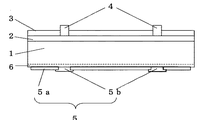
一般的な太陽電池素子の構造を図1に示す。多結晶シリコンなどのp型の半導体基板1の受光面側の表面近傍に一定の深さまで逆導電型のn型不純物(例えばP)を拡散させて、n型を呈する逆導電型領域2を設け、p型の半導体基板1との間にpn接合を形成する。この逆導電型領域2の上には、窒化シリコン膜などから成る反射防止膜3が設けられている。そして、受光面側である表面には表面電極4が設けられ、裏面にはアルミニウムなどから成る集電電極5aと銀などから成る出力取出電極5bとで構成される裏面電極5が設けられている。なお集電電極5の形成と同時に、半導体基板1の裏面にはアルミニウムが拡散され裏面電界領域(高濃度p+領域)6が形成される。
The structure of a general solar cell element is shown in FIG. A reverse
これらの太陽電池素子の表面電極4、裏面電極5は、金属を主成分とする電極材料を塗布・乾燥して焼成することによって得ることができる。
The
例えば、表面電極4、裏面電極5を形成する方法として、特許文献1などに以下の方法が記載されている。
For example, as a method of forming the
(1)集電電極5aを形成するために、アルミニウムなどを主成分とする電極材料を半導体基板1の裏面の一部を除いた大部分に塗布して乾燥する
(2)出力取出電極5bを形成するために、(1)で電極材料を塗布しなかった部分とその周縁部のアルミニウムに銀などを主成分とする電極材料を塗布して乾燥する
(3)表面電極4を形成するために、半導体基板1の表面に銀などを主成分とする電極材料を塗布して乾燥する
(4)表面と裏面に塗布された電極材料を同時に焼成し、表面電極4および裏面電極5を得る
上述の方法は、表面電極4および裏面電極5を同時に焼成する方法(同時焼成法)であるが、別々に焼成するようにしても良い。(例えば、特許文献2参照)
また、銀を主成分とするはんだ濡れ性の良好な表面電極4および裏面電極5(アルミニウムを主成分とする集電電極5aと銀を主成分とするはんだ濡れ性の良好な出力取出電極5b)が形成される。このとき、裏面の略全面に形成された集電電極5aは、シリコンの半導体基板1に対してp型不純物元素として作用するアルミニウムを主成分としているので、集電電極5aと接した部分には、裏面電界領域(高濃度p+領域)6が形成される。この裏面電界領域6は太陽電池特性を向上させる効果がある。
(1) In order to form the collector electrode 5a, an electrode material mainly composed of aluminum or the like is applied to most of the
Also, the
なお、上述したように半導体基板に電極材料を塗布した後に焼成するが、この焼成には、連続式の焼成炉を用いるのが一般的である。連続式の焼成炉を用いることによって、連続的に多くの半導体基板を焼成処理することができ、極めて生産性が高い。 As described above, the electrode material is applied to the semiconductor substrate and then baked. In general, a continuous baking furnace is used for this baking. By using a continuous firing furnace, many semiconductor substrates can be continuously fired, and productivity is extremely high.
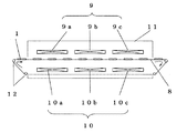
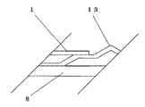
このような連続式の焼成炉の一例として、ベルト式連続焼成炉がある。このベルト式連続焼成炉は、焼成炉の加熱部を貫通させた搬送用ベルト上に半導体基板を配置し、エンドレスに搬送用ベルトを回転させることによって、焼成炉の加熱部の中を通過させて、焼成を行うものである。図3はベルト式連続焼成炉の構造を説明するための図であり、8は搬送用ベルト、9は上部ヒーター、10は下部ヒーター、11はカバー、12はローラーを示す。半導体基板1を処理する焼成炉は、断熱性や安全性、そして雰囲気を外気と遮断するために設けられたカバー11の中に、上部ヒーター9(9a〜9c)と下部ヒーター10(10a〜10c)が搭載されている。この上部ヒーター9と下部ヒーター10は遠赤外や近赤外等のヒーターで、抵抗コイルやランプなどからなる。この焼成炉の長手方向に炉を貫通して搬送用ベルト8が設けられ、この搬送用ベルト8は、ローラー12が回転駆動することによってエンドレスに循環し、これによって搬送用ベルト8上に乗せた半導体基板1が所定時間を費やして焼成炉内を通過し、その間に焼成が行われる。
An example of such a continuous firing furnace is a belt-type continuous firing furnace. In this belt-type continuous firing furnace, a semiconductor substrate is placed on a conveyor belt that penetrates the heating section of the firing furnace, and the conveyor belt is rotated endlessly, thereby passing through the heating section of the firing furnace. , Firing. FIG. 3 is a view for explaining the structure of a belt-type continuous firing furnace, wherein 8 is a conveying belt, 9 is an upper heater, 10 is a lower heater, 11 is a cover, and 12 is a roller. The firing furnace for processing the
通常、搬送用ベルト8は耐熱性や強度の観点から金属材料によって構成される。しかしながら、ペースト状の電極材料を搬送用ベルト側に塗布した半導体基板1を搬送用ベルト8の上に直接載置した場合、焼成時の加熱により、焼結していない電極材料が搬送用ベルト8の金属と合金化してしまう。そのため、半導体基板1が搬送用ベルト8に貼りついてしまうといった問題があった。このような場合、無理に剥がそうとすれば半導体基板1を破損し、また、搬送用ベルト8の寿命を縮めてしまう。
Usually, the
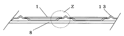
この問題に対し解決手段の一例として、特許文献3に記載されているベルト形状を図4、5に示す。図4はこのときの半導体基板と、搬送用ベルトの位置関係を示しており、図4において半導体基板は、搬送用ベルト8の進行方向に直角な向きの断面を示す。また、図5は図4のZ部の拡大図を示している。同文献には、半導体基板1と搬送用ベルトとの接触面積を少なくするために、半導体基板1の対向する二辺を支持して、半導体基板1と、搬送用ベルト8との間に空間領域を形成することで問題を解消することが記載されている。図5に示されるように半導体基板1は搬送用ベルト8の上に設けられた支持部材13の略凸型の突出部の段部で保持される。ゆえに、図4に示されるように半導体基板1の対向する二辺を支持して、半導体基板1と搬送用ベルト8との間に空間領域を形成することによって、半導体基板1と搬送用ベルト8との接触面積が小さくなる。したがって、半導体基板1の全面が搬送用ベルト8と触れるということがないため、焼成時の加熱によって電極材料が搬送用ベルト8に貼りつくことなく焼成が行われる。
半導体基板は、焼成される際に、局所的に熱履歴が異なるため、基板内に内部応力が生じ反りの原因となる。近年、太陽電池素子を形成するための半導体基板は大型化の傾向にあり、一般的に10cm×10cmから15cm×15cm程度の大きさを有している。さらに、コスト削減の観点から、半導体材料の使用量を削減するために、半導体基板の厚みが薄くなってきている。このように大型化した薄い半導体基板は、電極などを焼成によって形成したときに、半導体基板内の熱履歴の違いにより、形成状態に違いが生じることがある。また反りやすく、衝撃やストレスに対して弱いため、割れや欠けが生じ歩留まりが低下するなどの問題が発生することがあった。 When the semiconductor substrate is baked, the thermal history is locally different, so that internal stress is generated in the substrate and causes warping. In recent years, a semiconductor substrate for forming a solar cell element has been increasing in size, and generally has a size of about 10 cm × 10 cm to 15 cm × 15 cm. Furthermore, from the viewpoint of cost reduction, the thickness of the semiconductor substrate has been reduced in order to reduce the amount of semiconductor material used. A thin semiconductor substrate that is enlarged in this manner may have a difference in formation state due to a difference in thermal history in the semiconductor substrate when an electrode or the like is formed by baking. Moreover, since it is easy to warp and is vulnerable to impacts and stress, problems such as cracking and chipping and a decrease in yield may occur.
本発明はこれらの従来技術の問題点に鑑みてなされたものであり、電極の焼成時の加熱により太陽電池素子を構成する半導体基板内に与えられる内部応力を抑制し、半導体基板の反りを緩和することのできる太陽電池素子の製造方法を提供することを目的とする。 The present invention has been made in view of these problems of the prior art, and suppresses internal stress applied to the semiconductor substrate constituting the solar cell element by heating at the time of firing the electrode, thereby mitigating warpage of the semiconductor substrate. It aims at providing the manufacturing method of the solar cell element which can do.
上記目的を達成するために、本発明の請求項1に係る太陽電池素子の製造方法は、表面と裏面とを有する半導体基板と、前記表面に設けられた表面電極と、前記裏面に設けられた裏面電極とを含む太陽電池素子の製造方法であって、前記半導体基板に電極材料を塗布し、この半導体基板を焼成して前記表面電極および/または前記裏面電極を形成する電極形成工程を含むとともに、前記電極形成工程は、入口付近から温度が上昇して最高温度に達した後、下流に向かうに連れて温度が低下する温度分布を有する、連続式の焼成炉を用いて行う工程であり、前記半導体基板を略水平に配置して前記焼成炉内を通過させて焼成する第一焼成工程と、前記半導体基板を、鉛直方向を軸として前記第一焼成工程で焼成した向きから略90°回転させた状態で、前記焼成炉内を再度通過させて焼成する第二焼成工程と、を含む。
In order to achieve the above object, a method for manufacturing a solar cell element according to
ここで、本発明の請求項2に係る太陽電池素子の製造方法は、請求項1に記載の太陽電池素子において前記裏面電極は、前記半導体基板の裏面の略全面に形成された集電電極とこの集電電極に接続された出力取出電極と、を含むようにした。
Here, the method for manufacturing a solar cell element according to
また、本発明の請求項3に係る太陽電池素子の製造方法は、請求項2に記載の太陽電池素子の製造方法において、前記集電電極は、前記第一焼成工程および前記第二焼成工程を経て形成される。
Moreover, the manufacturing method of the solar cell element which concerns on
そして、本発明の請求項4に係る太陽電池素子の製造方法は、請求項3に記載の半導体基板において、前記集電電極との間に、この半導体基板と同じ導電型でより高濃度の不純物を含む裏面電界領域を有するとともに、この領域は前記第一焼成工程および前記第二焼成工程によって形成される。
And the manufacturing method of the solar cell element which concerns on
また、本発明の請求項5に係る太陽電池素子の製造方法は、請求項4に記載の太陽電池素子の製造方法において、前記半導体基板は、p型シリコン半導体であり、前記集電電極は、アルミニウムを主成分として形成される。
The method for manufacturing a solar cell element according to
さらに、本発明の請求項6に係る太陽電池素子の製造方法は、請求項1から請求項5のいずれか一項に記載の太陽電池素子の製造方法において、前記第一焼成工程と前記第二焼成工程との間に前記半導体基板を表裏反転させる工程を設けた。
Furthermore, the manufacturing method of the solar cell
さらに、本発明の請求項7に係る太陽電池素子の製造方法は、請求項1から請求項6のいずれか一項に記載の太陽電池素子の製造方法において、前記第一焼成工程および前記第二焼成工程は、エンドレスに回転する搬送用ベルトを備えたベルト式連続焼成炉を用い、前記搬送用ベルト上に前記半導体基板を配置した状態で行われる。 Furthermore, the manufacturing method of the solar cell element concerning Claim 7 of this invention is a manufacturing method of the solar cell element as described in any one of Claims 1-6, Said 1st baking process and said 2nd. The firing step is performed using a belt-type continuous firing furnace having a transport belt that rotates endlessly, and the semiconductor substrate is disposed on the transport belt.
また、本発明の請求項8に係る太陽電池素子の製造方法は、請求項7に記載の太陽電池素子の製造方法において、前記ベルト式連続焼成炉は、前記搬送用ベルトを挟んで、上方と下方にそれぞれ上部ヒーターと下部ヒーターとを備える。
Moreover, the manufacturing method of the solar cell element according to
そして、本発明の請求項9に係る太陽電池素子の製造方法は、請求項6に記載の太陽電池素子の製造方法において、前記半導体基板は、前記電極形成工程において、前記下部ヒーターから受ける熱量よりも前記上部ヒーターから受ける熱量の方が大きくなるようにした。
And the manufacturing method of the solar cell element which concerns on
上述のように本発明は、表面と裏面とを有する半導体基板と、前記表面に設けられた表面電極と、前記裏面に設けられた裏面電極とを含む太陽電池素子の製造方法であって、前記半導体基板に電極材料を塗布し、この半導体基板を焼成して前記表面電極および/または前記裏面電極を形成する電極形成工程を含むとともに、前記電極形成工程は、前記半導体基板を略水平に配置して焼成する第一焼成工程と、前記半導体基板を、鉛直方向を軸として前記第一焼成工程で焼成した向きから略90°回転させた状態で焼成する第二焼成工程と、を含むため、半導体基板の一部分に集中して大きな熱量がかかることを防ぐことができる。その結果、熱履歴の違いで半導体基板に蓄積する内部応力を抑制し、形成状態を均一化した太陽電池素子を得ることができる。 As described above, the present invention is a method of manufacturing a solar cell element including a semiconductor substrate having a front surface and a back surface, a front surface electrode provided on the front surface, and a back electrode provided on the back surface, The electrode forming step includes applying an electrode material to a semiconductor substrate and firing the semiconductor substrate to form the front surface electrode and / or the back electrode, and the electrode forming step includes disposing the semiconductor substrate substantially horizontally. A first baking step of baking and a second baking step of baking the semiconductor substrate in a state where the semiconductor substrate is rotated by about 90 ° from the direction of baking in the first baking step with the vertical direction as an axis. It is possible to prevent a large amount of heat from being concentrated on a part of the substrate. As a result, a solar cell element in which the internal stress accumulated in the semiconductor substrate due to the difference in thermal history is suppressed and the formation state is made uniform can be obtained.
以下、本発明を添付図面に基づき詳細に説明する。 Hereinafter, the present invention will be described in detail with reference to the accompanying drawings.
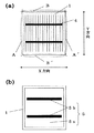
図1は本発明の太陽電池素子の製造方法に係る太陽電池素子の構造の一例を示す断面図であり、図2(a)は図1に示した太陽電池素子の表面電極を示す上視図、図2(b)は図1に示した太陽電池素子の裏面電極を示す下視図である。なお、図中、1は半導体基板、2は逆導電型領域、3は反射防止膜、4は表面電極、5は裏面電極、5aは集電電極、5bは出力取出電極、6は裏面電界領域を示す。 FIG. 1 is a cross-sectional view showing an example of the structure of a solar cell element according to the method for manufacturing a solar cell element of the present invention, and FIG. 2 (a) is a top view showing a surface electrode of the solar cell element shown in FIG. FIG. 2B is a bottom view showing the back electrode of the solar cell element shown in FIG. In the figure, 1 is a semiconductor substrate, 2 is a reverse conductivity type region, 3 is an antireflection film, 4 is a surface electrode, 5 is a back electrode, 5a is a current collecting electrode, 5b is an output extraction electrode, and 6 is a back surface electric field region. Indicates.
ここで、図1に示す太陽電池素子の作用について簡単に説明する。 Here, the effect | action of the solar cell element shown in FIG. 1 is demonstrated easily.
太陽電池素子の受光面側である反射防止膜3の側から光が入射すると、主にp型半導体である半導体基板1のバルク領域で吸収・光電変換されて電子−正孔対(電子キャリアおよび正孔キャリア)が生成される。この光励起起源の電子キャリアおよび正孔キャリア(光生成キャリア)によって、太陽電池素子の表側に設けられた表面電極4と、裏側に設けられた裏面電極5との間に光起電力を生ずる。なお、反射防止膜3は反射防止膜となる膜の屈折率と膜厚とによって所望の光波長領域で反射率を低減させて、光生成キャリア量を増大させる役割を果たし、太陽電池素子の光電流密度Jscを向上させる。
When light is incident from the side of the
また、裏面電極5の集電電極5aは、通常、半導体基板であるシリコンに対して、p型不純物元素として作用するアルミニウムを用いて形成されるので、シリコン基板の裏面側表層部にp+領域となった裏面電界領域6を形成する。裏面電界領域6は、BSF(Back Surface Field)領域とも呼ばれ、半導体基板1の裏面近くで光生成キャリアによる再結合による効率の低下を防ぐ。そのため半導体基板1の裏面近くで発生した光生成キャリアが、この電界によって加速される結果、電力が有効に取り出されることとなり、特に長波長の光感度が増加する。この結果、光電流密度Jscが向上し、またこの裏面電界領域6では少数キャリア(電子)密度が低減されるので、裏面電極5に接する領域でのダイオード電流量(暗電流量)を低減する働きをすることで、開放電圧Vocが向上する。
Further, since the current collecting electrode 5a of the
次に上述の構造を有する太陽電池素子の製造工程について説明する。半導体基板1は、単結晶又は多結晶シリコンなどから成る。この半導体基板1として半導体シリコンを用いる場合、ボロン(B)、ガリウム(Ga)などのp型の導電型を呈する半導体不純物を1×10¹⁶〜1018atoms/cm3程度含有し、比抵抗1.0〜2.0Ω・cm程度の基板が好適に用いられる。単結晶シリコン基板の場合は引き上げ法などによって形成され、多結晶シリコン基板の場合は鋳造法などによって形成される。多結晶シリコン基板は、大量生産が可能であり製造コスト面で単結晶シリコン基板よりも有利であるので、ここでは多結晶シリコンを用いた例によって説明する。
Next, the manufacturing process of the solar cell element having the above structure will be described. The
多結晶シリコンのインゴットは、例えば、鋳造法によって形成され、300μm程度の厚みにスライスして、10cm×10cmまたは15cm×15cm程度の大きさに切断され、半導体基板1とする。なお、基板の切断面を清浄化するために表面をフッ酸やフッ硝酸などでごく微量エッチングすることが望ましい。
The polycrystalline silicon ingot is formed by, for example, a casting method, sliced to a thickness of about 300 μm, and cut into a size of about 10 cm × 10 cm or 15 cm × 15 cm to form the
その後、ドライエッチング方法やウェットエッチング方法を用いて、シリコン基板の表面に微小な突起を形成するのが望ましい。 Thereafter, it is desirable to form minute protrusions on the surface of the silicon substrate using a dry etching method or a wet etching method.
次に、半導体基板1を拡散炉中に配置して、オキシ塩化リン(POCl3)などの不純物元素を含むガス中で熱処理することによって、半導体基板1の外表面部分にリン原子を拡散させてシート抵抗が30〜300Ω/□程度のn型の導電型を呈する逆導電型領域2を形成する。
Next, the
そして、太陽電池素子の受光面側である半導体基板1の表面側に、逆導電型領域2を残して他の部分を除去した後、純水で洗浄する。この除去方法としては、例えば、半導体基板1の表面側にフッ酸に耐性を有するレジスト膜を塗布し、フッ酸と硝酸の混合液を用いてこの半導体基板1の表面側以外の逆導電型領域をエッチング除去した後、レジスト膜を除去すればよい。
And after removing other portions on the surface side of the
次に、半導体基板1の表面側に反射防止膜3を形成する。この反射防止膜3は例えば窒化シリコン膜などから成り、例えばシラン(SiH4)とアンモニア(NH3)との混合ガスをグロー放電分解でプラズマ化させて堆積させるプラズマCVD法などで形成される。この反射防止膜3は、半導体基板1との屈折率差などを考慮して、屈折率が1.8〜2.3程度になるように形成され、厚み500〜1000Å程度の厚みに形成される。このように窒化シリコン膜を、水素プラズマの存在下で成膜して形成した場合、パッシベーション効果も同時に有するので、反射防止の機能と併せて、太陽電池の電気特性を向上させる効果がある。
Next, an
そして、本発明に係る電極形成工程により、表面電極4と、集電電極5aと出力取出電極5bとを含む裏面電極5を以下のようにして形成する。
And by the electrode formation process which concerns on this invention, the
裏面電極5を構成する集電電極5aは、例えばアルミニウム粉末などからなる金属と有機ビヒクルとガラスフリットをアルミニウム100重量部に対してそれぞれ10〜30重量部、0.1〜5重量部を添加してペースト状にした電極材料を用いる。具体的な形状としては、例えば、図2(b)に示すように、後述する出力取出電極5bを形成する部位を除いた裏面のほぼ全面に集電電極5aを形成する。塗布法としては、スクリーン印刷法などの周知の方法を用いることができ、塗布後、所定の温度で溶剤を蒸散させて乾燥させる。
The collector electrode 5a constituting the
裏面電極5を構成する出力取出電極5bおよび表面電極4は、半田濡れ性のよい金属材料、例えば銀粉末などと有機ビヒクルとガラスフリットを銀100重量部に対してそれぞれ10〜30重量部、0.1〜5重量部を添加してペースト状にした電極材料を用いる。具体的な形状としては、例えば、図2(a)、(b)に示すように、表面電極4は格子状に形成し、出力取出電極5bは、大部分が上述のアルミニウムを主成分とした集電電極5aを塗布しなかった部位に設けられ、周縁部を集電電極5aと重ね合わせて形成する。塗布法としては、スクリーン印刷法などの周知の方法を用いることができ、塗布後、所定の温度で溶剤を蒸散させて乾燥させる。
The output extraction electrode 5b and the
上述のようにして塗布・乾燥した表面電極4、裏面電極5を、後述する本発明の第一焼成工程・第二焼成工程を経ることによって、半導体基板に対して電極を焼き付けて形成することができる。
The
なお、以下に示す焼成方法では、図3に示すベルト式連続焼成炉の構造を用いて説明を行う。図3中、8は搬送用ベルト、9(9a、9b、9c)は上部ヒーター、10(10a、10b、10c)は下部ヒーター、11はカバー、12はローラーを示す。 The firing method described below will be described using the structure of a belt-type continuous firing furnace shown in FIG. In FIG. 3, 8 is a conveyance belt, 9 (9a, 9b, 9c) is an upper heater, 10 (10a, 10b, 10c) is a lower heater, 11 is a cover, and 12 is a roller.
半導体基板1を処理するベルト式連続焼成炉は、断熱性や安全性、そして雰囲気を外気と遮断するために設けられたカバー11の中に、複数の上部ヒーター9(9a、9b、9c)と下部ヒーター10(10a、10b、10c)が搭載されている。この上部ヒーター9と下部ヒーター10は遠赤外や近赤外等のヒーターで、抵抗コイルやランプなどからなる。
The belt-type continuous firing furnace for processing the
このベルト式連続焼成炉の長手方向に炉を貫通して搬送用ベルト8が設けられ、この搬送用ベルト8は、ローラー12が回転駆動することによって循環し、これによって搬送用ベルト8上に乗せた半導体基板1が焼成炉内を通過する。
A
このようなベルト式連続焼成炉によって、半導体基板1に塗布した電極材料を焼成する場合、通常、入口付近から急激に温度が上昇し、最高温度となる600〜800℃まで上昇し、最高温度に達した後は、徐々に温度を低下させる温度分布となっている。これは最初に電極材料の焼結に必要な温度まで達した後、急冷による応力に起因する太陽電池素子の割れを防ぐためである。具体的には、ベルト式連続焼成炉の入口側の上部ヒーター9a、下部ヒーター10aを熱の流出を考慮して最高温度より高めの温度に設定し、上部ヒーター9b、9cおよび下部ヒーター10b、10cを半導体基板1が下流に向かうに連れて、徐々に温度を低下させるような設定にすればよい。
When the electrode material applied to the
以下、本発明の太陽電池の製造方法に係る第一焼成工程・第二焼成工程の各焼成工程の実施形態において図2を用いて説明する。図2(a)は半導体基板1の表面方向から見た図である。この半導体基板1表面において一辺をAとし、Aと平行に対向する一辺はA’とする。また、残りのB、B’はそれぞれ対向しており平行する位置関係にある。ここで、辺A、A’と平行な方向をY方向、辺B、B’と平行な方向をX方向とした。
Hereinafter, an embodiment of each firing step of the first firing step and the second firing step according to the solar cell manufacturing method of the present invention will be described with reference to FIG. FIG. 2A is a diagram viewed from the surface direction of the
上記電極形成工程は、前記半導体基板に電極材料を塗布し、半導体基板を焼成して前記表面電極および/または前記裏面電極を形成するものである。そして、半導体基板1を略水平に配置して焼成する第一焼成工程と、半導体基板1を、鉛直方向を軸として第一焼成工程で焼成した向きから略90°回転させた状態で焼成する第二焼成工程と、を含む太陽電池素子の製造方法である。焼成炉を通過させる第一焼成工程では、ベルトに載持された半導体基板1の進行方向がX方向で、辺Aが先に焼成炉に進入する場合、Aと対向する辺A’が焼成炉に進入するまでに時間差がある。また、このとき辺B、B’については、B、B’両辺ともほぼ同時に加熱されていくため、熱履歴の時間的差異は少ない。
In the electrode forming step, an electrode material is applied to the semiconductor substrate, and the semiconductor substrate is baked to form the front electrode and / or the back electrode. Then, a first baking step in which the
そして、焼成炉を再度通過させる第二焼成工程では、第一焼成工程での向きから90°回転させているため、半導体基板1はY方向に進行する。第二焼成工程においては逆に、辺A、A’は、同時に加熱されるために熱履歴の差は少ない。また、辺B、B’については、焼成炉に進入するまでに時間差がある。ゆえに、半導体基板1が第一焼成工程で生じた熱履歴と、第二焼成工程で生じた熱履歴のバランスをとって内部応力の均一化を図ることができるため、半導体基板1の反りを緩和することができる。
And in the 2nd baking process which passes a baking furnace again, since it rotated 90 degrees from the direction in a 1st baking process, the
次に、集電電極5aは第一焼成工程および第二焼成工程を経て形成されるようにすることが望ましい。その理由は以下の通りである。まず、集電電極5aの面積は広く、使用する電極材料の量も多い。したがって、半導体基板1と電極材料との熱膨張係数の差異による影響を大きく受けるので、半導体基板1の反りに対して及ぼす影響が大きい。ここで本発明に係る第一焼成工程・第二焼成工程の各焼成工程により、上述したような理由から、基板に対する熱履歴をより均一化できるので、基板が一方向へ大きく反ることなく、両方向へ均等に反るようになる。その結果、大きな反りを抑制することができるので、反りによる半導体基板1の割れを軽減することができる。さらに、半導体基板1と集電電極5aのオーミック接触は第一焼成工程、第二焼成工程を経た後で、より安定性を増すからである。
Next, it is desirable that the collecting electrode 5a is formed through the first firing step and the second firing step. The reason is as follows. First, the current collecting electrode 5a has a large area and a large amount of electrode material is used. Therefore, since it is greatly affected by the difference in thermal expansion coefficient between the
また、集電電極5aは半導体基板1と同じ導電型を呈する半導体不純物を含んだ電極材料を用い、第一焼成工程と第二焼成工程を経ることによって半導体基板1と集電電極5aとの間にこの半導体基板1と同じ導電型でより高濃度の不純物を含む裏面電界領域6が略全面に形成される。この裏面電界領域6は、光生成電子キャリアが半導体基板1から裏面電極5に到達して再結合損失する割合を低減する役割を果たし、光電流密度Jscを向上させる働きをもつ。また、裏面電界領域6では少数キャリア(電子)密度が低減されるので、この領域および裏面電極5に接する領域でのダイオード電流量(暗電流量)を低減する働きをし、開放電圧Vocが向上するという効果が得られ、太陽電池素子の特性を向上させることができる。
Further, the current collecting electrode 5a is made of an electrode material containing a semiconductor impurity having the same conductivity type as that of the
ここで、半導体基板1としてp型シリコン半導体を用いた場合、集電電極5aの電極材料として、アルミニウムを主成分とするものを用いることが望ましい。上述のように電極材料にアルミニウムを主成分とした集電電極5aを焼成することにより、集電電極6とシリコン基板の接合部分においてアルミニウムがシリコン基板の内部に熱拡散し、シリコン基板はp型不純物であるアルミニウムを多量に含んだ裏面電界領域(高濃度p+領域)6を形成させることができる。
Here, when a p-type silicon semiconductor is used as the
そして、第一焼成工程と第二焼成工程との間に半導体基板1を表裏反転させる表裏反転工程を設けることが望ましい。このように、第一焼成工程と第二焼成工程との間に半導体基板1を、第一焼成工程で焼成した状態から表裏反転させることによって、半導体基板1が焼成炉内部から受ける熱の影響を分散させ内部応力の均一化を図ることができる。
And it is desirable to provide the front-back inversion process which reverses the
さらに、第一焼成工程と第二焼成工程との間に、表裏反転工程を含んだ場合、
(1)第一焼成工程時には半導体基板1の受光面側の表面に何も存在していない状態で搬送用ベルト8に配置し、裏面側電極を焼成する
Furthermore, when a front / back reversal step is included between the first firing step and the second firing step,
(1) During the first firing step, the
(2)半導体基板1の受光面側に表面電極4を塗布乾燥させて設ける
(3)表裏反転工程の後、第二焼成工程で半導体基板1の表面電極4の側を焼成する
このような手順で焼成を行えば、表面電極4と搬送用ベルト8との接触を防ぎ、半導体基板1の受光面側の汚れを防止し、受光量の減少を防ぐことができる。
(2) The
また、第一焼成工程と、第二焼成工程においては、エンドレスに回転する搬送用ベルトを備えたベルト式連続焼成炉を用い、搬送用ベルト8上に半導体基板1を配置した状態で行うようにすることが望ましい。
Further, in the first firing step and the second firing step, a belt-type continuous firing furnace having a transport belt that rotates endlessly is used, and the
これは、エンドレスに回転する搬送用ベルトを備えたベルト式連続焼成炉を用いることで大量生産が可能となり、コストの面でも非常に有用であるためである。 This is because mass production is possible by using a belt-type continuous firing furnace provided with an endlessly rotating conveyor belt, which is very useful in terms of cost.
そして、この搬送用ベルト8を含む焼成炉は搬送用ベルト8を挟んで、上方と下方とにそれぞれ上部ヒーター9と下部ヒーター10とを備えたものが望ましい。上部ヒーター9と下部ヒーター10を備えたベルト式焼成炉の場合、電極形成において表面電極4、裏面電極5など同時に焼成することが可能となるためである。
The firing furnace including the
ここで、このような上部ヒーター9と下部ヒーター10を用いたベルト式連続焼成炉を用いる場合、半導体基板1が各焼成工程において受ける熱量は、下部ヒーター10よりも上部ヒーター9から受ける方が大きくなるようにすることが望ましい。このような構成にすれば、上方と下方からの加熱状態が非対称となり、各焼成工程における半導体基板1の内部の温度分布の対称性を崩すことができる。その結果、本発明の実施形態における効果をより確実なものとし、半導体基板内部の熱履歴をより分散させ形成状態を均一化できる。
Here, when such a belt-type continuous firing furnace using the
その理由として、下部ヒーター10は搬送用ベルト8を挟んで半導体基板1の下面(搬送用ベルト8と接した面)と対向しており、直接、半導体基板1の上面と向き合った上部ヒーター9に比べて、半導体基板1に高い熱量を供給することが難しい。もちろん、電力を増大させることによって可能ではあるが、より搬送用ベルト8が加熱されることなり、エネルギーの効率的利用という観点から見ても、上部ヒーター9からの熱量を大きくする方が自然であり、より好ましい。
The reason is that the
また、第二焼成工程の前に半導体基板1の表裏反転工程を設けた第一焼成工程もしくは、第二焼成工程において、必ず半導体基板1の表面側を、より受ける熱量が少ない下部ヒーター10に向けて焼成することになる。ゆえに、半導体基板1の表面側へ必要以上に熱量がかからないため、逆導電型領域2へのダメージを軽減することができ、出力特性が良好な太陽電池素子を得ることが可能である。
Moreover, in the 1st baking process which provided the front-and-back inversion process of the
上述のように上部ヒーター9、下部ヒーター10を用いたベルト式連続焼成炉を用いる場合、半導体基板1が各焼成工程において受ける熱量について、下部ヒーター10よりも上部ヒーター9から受ける方が大きいかどうかについては、次のようにして確認することができる。
As described above, when the belt-type continuous firing furnace using the
(a)ダミーの半導体基板の表面および裏面の複数箇所(表裏の対称箇所)に熱電対を取り付ける
(b)上部ヒーター9と下部ヒーター10を所定の温度条件に設定する
(c)(a)のダミーの半導体基板を搬送用ベルト8に配置し、所定のベルト速度で送る
(d)熱電対によって、ダミーの半導体基板の表面および裏面の温度を測定し、温度のプロファイルを作成する
(e)(d)で作成された温度のプロファイルを時間で積分したものを表面、裏面で比較し、加えられた熱量を比較する(複数箇所について平均値を取る)
特許文献3には、焼成時の加熱により、焼結していない電極材料が搬送用ベルト8の金属と合金化するのを防ぐために、半導体基板1の対向する二辺を支持して、半導体基板1と、搬送用ベルト8との間に空間領域を形成することが記載されている。図4はこのときの半導体基板と、搬送用ベルトの位置関係を示しており、図4において半導体基板は、搬送用ベルト8の進行方向に直角な向きの断面を示す。また、図5は図4のZ部の拡大図を示している。図5に示されるように半導体基板1は搬送用ベルト8の上に設けられた支持部材13の略凸型の突出部の段部で保持される。ゆえに、図4に示されるように半導体基板1の対向する二辺を支持して、半導体基板1と搬送用ベルト8との間に空間領域を形成することによって、半導体基板1と搬送用ベルト8との接触面積が小さくなる。したがって、半導体基板1の全面が搬送用ベルト8と触れるということがないため、焼成時の加熱によって電極材料が搬送用ベルト8に貼りつくことなく焼成が行われる。
(A) A thermocouple is attached to a plurality of locations (symmetric locations on the front and back sides) of the front and back surfaces of the dummy semiconductor substrate. (B) The
In
上述のように半導体基板1の対向する二辺を支持して電極を焼成によって形成する場合、半導体基板を加熱すると同時に搬送用ベルト8ならびに支持部材13も加熱される。太陽電池素子を構成する半導体基板1は、搬送用ベルト8に載置される際、半導体基板1の対向する二辺(例えば、図2に示されるA、A´)を支持部材13によって保持するため、半導体基板において支持部材13と直接接触している部分A、A´と、接触していない部分B、B´とでは、昇温速度が異なり、その結果、基板内、特に半導体基板のA、A´側とB、B´側とでは熱履歴の違いが生じ、熱履歴の違いによる内部応力によって基板に反りが発生する。
When the electrodes are formed by firing while supporting the two opposing sides of the
しかしながら、本発明の実施形態では、この焼成工程として、半導体基板1を焼成するときに、第一焼成工程において、半導体基板1の進入方向がX方向で図2(a)に示される半導体基板1のA、A´側を搬送用ベルト8の支持部材13に載置し、略水平に配置した状態で焼成を行い、第二焼成工程においては、半導体基板1を、鉛直方向を軸として第一焼成工程で焼成した向きから略90°回転させ、半導体基板1の進入方向がY方向で図2(a)に示される半導体基板1のB、B´側を搬送用ベルト8の支持部材13に載置し、焼成する。これによって、第一焼成工程で半導体基板1に対して加えられた熱履歴とは異なった熱履歴が第二焼成工程によって加えられるので、より広い領域で、特にA、A´側とB、B´側において均一に熱が印加されることとなる。そして、一部分に必要以上の熱量が印加されないため、内部応力が緩和され、基板の反りが緩和された太陽電池素子を得ることができる。
However, in the embodiment of the present invention, when the
なお、本発明の実施形態は上述の例にのみ限定されるものではなく、本発明の要旨を逸脱しない範囲内において種々変更を加え得ることはもちろんである。 It should be noted that the embodiment of the present invention is not limited to the above-described example, and it is needless to say that various modifications can be made without departing from the gist of the present invention.
例えば、上述の説明では大量生産が可能である例をとってベルト式焼成炉を用いた説明したが、これに限るものではなく、バッチ式焼成炉においても前記のように第一焼成工程と、第二焼成工程との間で半導体基板の向きを90°回転させる工程および/または半導体基板を鉛直方向に表裏反転させる表裏反転工程を含ませることが同様に有効である。 For example, in the above description, the belt-type firing furnace has been described using an example in which mass production is possible. However, the present invention is not limited to this, and the batch firing furnace also includes the first firing step as described above, It is also effective to include a step of rotating the direction of the semiconductor substrate by 90 ° between the second baking step and / or a front / back reversing step of reversing the semiconductor substrate in the vertical direction.
この理由として、バッチ式焼成炉内での焼成温度は不均一であり、第二焼成工程において半導体基板1を鉛直方向に90°回転させた工程を含むことで、半導体基板1が受ける熱が一部分に集中するのを防ぐ。この結果、半導体基板の内部応力を分散させることが可能となり、形成状態を均一化した半導体基板ができる。
The reason for this is that the firing temperature in the batch-type firing furnace is non-uniform, and the heat received by the
そして、表面電極4は、あらかじめ反射防止膜3の表面電極4に相当する部分をエッチングし、その箇所に電極材料(銀ペーストなど)を塗布し、焼成して逆導電型領域2と導通を取るようにしてもよい。また、反射防止膜3の上に直接電極材料(銀ペーストなど)を塗布して焼成し、いわゆるファイアースルー法によって反射防止膜3を貫通させて逆導電型領域2と導通を取るようにしてもよい。
The
次に、電極焼成順序の観点から見れば、半導体基板1の表面には表面電極4を設けられており、裏面に裏面電極5を設けられているが、裏面電極5には略全面に形成された集電電極5aと、この集電電極5aに接続された出力取出電極5bとを含んでいる。これらの電極を形成する焼成の順番、組み合わせは上記に示した方法以外であっても構わない。例えば、第一焼成工程で裏面電極5(集電電極5aと出力取出電極5b)を形成し、第二焼成工程で表面電極4を形成してもよいし、第一焼成工程で出力取出電極5bを形成し、第二焼成工程で集電電極5aと表面電極4を形成してもよいが、集電電極5aは第一焼成工程および第二焼成工程を経て形成されるようにすることが望ましい。また、表面電極4は第一焼成工程および第二焼成工程を経て形成されてもよい。
Next, from the viewpoint of the electrode firing order, the
そして、搬送用ベルト8の入口側には焼成前の半導体基板1を連続的に搬送用ベルト8上に配置するローダー(不図示)を設け、さらに、搬送用ベルト8の出口側には、焼成後の半導体基板1を連続的に搬送用ベルト8からピックアップ可能なアンローダー(不図示)を設けてもよい。
A loader (not shown) for continuously disposing the
さらに、第一焼成工程と第二焼成工程は、それぞれ異なった焼成炉、望ましくはベルト
式連続焼成炉を用いて処理するようにすれば、高い生産性で大量の半導体基板を処理することができるので望ましい。この場合、第一焼成工程を終えた半導体基板に対して、鉛直方向を軸として略90°回転させたり、表裏反転させたりする機構を設けることが望ましい。例えば、アンローダーによって半導体基板をカセットに集約した後に、カセット自身を、鉛直方向を軸として略90°回転させたり、表裏反転させたりする機構を設け、その後、第二焼成工程に用いる焼成炉のローダーにこのカセットをセットして、半導体基板を所定状態で供給するようにすればよい。なお、あらかじめローダーに対して、カセットを所定状態でセットできるような構造にしておくことは言うまでもない。
Furthermore, if the first baking step and the second baking step are processed using different baking furnaces, preferably belt type continuous baking furnaces, a large amount of semiconductor substrates can be processed with high productivity. So desirable. In this case, it is desirable to provide a mechanism for rotating the surface of the semiconductor substrate after the first baking step by approximately 90 ° about the vertical direction or reversing the front and back. For example, after a semiconductor substrate is aggregated into a cassette by an unloader, a mechanism is provided to rotate the cassette itself about 90 ° about the vertical direction or to reverse the front and back, and then a firing furnace used for the second firing step What is necessary is just to set this cassette to a loader and to supply a semiconductor substrate in a predetermined state. Needless to say, the loader is previously structured so that the cassette can be set in a predetermined state.
さらに、ベルト式連続焼成炉について、図3では上部ヒーター9と下部ヒーター10の両方を記載したが、これに制限されるものではなく、上部ヒーター9のみや下部ヒーター10のみの構造でもよい。しかし、半導体基板1の両面に電極材料が塗布されている場合、上部ヒーター9と下部ヒーター10の両方を備えていれば、これらを用いることによって、同時に焼成を行うことができるのでより望ましい。これは、半導体基板1の表面電極4と裏面電極5とを同時に加熱焼成することができるからである。
Furthermore, in the belt-type continuous firing furnace, both the
なお、図3では上部ヒーター9、下部ヒーター10ともそれぞれ3分割にして記載したが、これに制限されるものではなく、これより多くても少なくても構わない。ただし、半導体基板1の加熱のプロファイルを自在に設定するためには、3分割以上とすることが望ましい。
In FIG. 3, each of the
また、上述の説明では、半導体基板1は下部ヒーター10に比べ上部ヒーター9の方から大きい熱量を受ける例によって説明した。通常、上部ヒーター9に比べ下部ヒーター10は搬送用ベルト8を挟んで半導体基板1に対峙しているので、上部ヒーター9からの熱量を大きくする方が簡単であるが、逆であっても何ら差し支えなく、ヒーターの取り付け位置も上部のみ、下部のみでもなんら差し支えない。これら、ヒーターの取り付け方によらず本発明による太陽電池素子の製造方法を用いれば、半導体基板への熱履歴を均一にし、半導体基板の反りを抑え、逆導電型領域2へのダメージを軽減することができる。
In the above description, the
同様に、上述の説明では、焼成工程として第一焼成工程および第二焼成工程のように二つの焼成工程を備えた例によって説明したが、これら二つの焼成工程の前後あるいは間に、更に複数の焼成工程を備えていても構わない。 Similarly, in the above description, the example in which two firing steps are provided as the firing step, such as the first firing step and the second firing step, has been described. You may provide the baking process.
また、第一焼成工程をはじめとする各焼成工程においては、半導体基板を略水平に配置するが、必ずしも厳密に水平である必要はない。例えば、ベルト式連続焼成炉の場合、排気を良くするために搬送用ベルトが傾斜を有している場合があるが、半導体基板が搬送用ベルトから滑り落ちない程度であれば、このような傾斜を有する状態で配置しても構わない。この場合、第二焼成工程では、半導体基板面に対して鉛直方向とする直交する方向を鉛直方向とみなして90°回転させ焼成すればよい。 Moreover, in each baking process including the first baking process, the semiconductor substrate is disposed substantially horizontally, but it is not necessarily required to be strictly horizontal. For example, in the case of a belt-type continuous firing furnace, the conveyor belt may have an inclination to improve exhaust, but such an inclination is sufficient if the semiconductor substrate does not slide off the conveyor belt. You may arrange | position in the state which has. In this case, in the second baking step, the direction orthogonal to the semiconductor substrate surface may be regarded as the vertical direction and rotated by 90 ° for baking.
また、半導体基板の材質は、シリコン以外に周知の化合物半導体であっても構わない。さらに、焼成する電極材料や塗布する電極形状、あるいは塗布方法についても、上述の例に限るものではなく、太陽電池素子としての特性を発揮できる材料や形状の組合せであれば、本発明の構成によって本発明特有の作用効果を得ることができることは言うまでもない。 The material of the semiconductor substrate may be a known compound semiconductor other than silicon. Further, the electrode material to be fired, the electrode shape to be applied, or the application method are not limited to the above-described examples, and any combination of materials and shapes that can exhibit the characteristics as a solar cell element can be used according to the configuration of the present invention. Needless to say, the advantages of the present invention can be obtained.
1:半導体基板
2:逆導電型領域
3:反射防止膜
4:表面電極
5:裏面電極
5a:集電電極
5b:出力取出電極
6:裏面電界領域
8:搬送用ベルト
9:上部ヒーター
9、9a、9b、9c:上部ヒーター
10、10a、10b、10c:下部ヒーター
11:カバー
12:ローラー
13:支持部材
1: Semiconductor substrate 2: Reverse conductivity type region 3: Antireflection film 4: Front electrode 5: Back electrode 5a: Current collecting electrode 5b: Output extraction electrode 6: Back surface electric field region 8: Conveying belt 9:
Claims (9)
前記半導体基板に電極材料を塗布し、この半導体基板を焼成して前記表面電極および/または前記裏面電極を形成する電極形成工程を含むとともに、
前記電極形成工程は、入口付近から温度が上昇して最高温度に達した後、下流に向かうに連れて温度が低下する温度分布を有する、連続式の焼成炉を用いて行う工程であり、
前記半導体基板を略水平に配置して前記焼成炉内を通過させて焼成する第一焼成工程と、前記半導体基板を、鉛直方向を軸として前記第一焼成工程で焼成した向きから略90°回転させた状態で、前記焼成炉内を再度通過させて焼成する第二焼成工程と、
を含む太陽電池素子の製造方法。 A method for manufacturing a solar cell element, comprising a semiconductor substrate having a front surface and a back surface, a front surface electrode provided on the front surface, and a back electrode provided on the back surface,
Including an electrode forming step of applying an electrode material to the semiconductor substrate and firing the semiconductor substrate to form the front electrode and / or the back electrode;
The electrode forming step is a step performed using a continuous firing furnace having a temperature distribution in which the temperature rises from the vicinity of the inlet to reach the maximum temperature and then decreases toward the downstream,
A first baking step in which the semiconductor substrate is disposed substantially horizontally and is fired by passing through the baking furnace, and the semiconductor substrate is rotated by about 90 ° from the direction of baking in the first baking step with the vertical direction as an axis. A second firing step in which the inside of the firing furnace is passed again and fired,
The manufacturing method of the solar cell element containing this.
ーターと下部ヒーターとを備えた請求項7に記載の太陽電池素子の製造方法。 The said belt-type continuous baking furnace is a manufacturing method of the solar cell element of Claim 7 provided with the upper heater and the lower heater in the upper direction and the downward direction on both sides of the said belt for conveyance.
Priority Applications (1)
| Application Number | Priority Date | Filing Date | Title |
|---|---|---|---|
| JP2004190463A JP4817618B2 (en) | 2004-06-28 | 2004-06-28 | Method for manufacturing solar cell element |
Applications Claiming Priority (1)
| Application Number | Priority Date | Filing Date | Title |
|---|---|---|---|
| JP2004190463A JP4817618B2 (en) | 2004-06-28 | 2004-06-28 | Method for manufacturing solar cell element |
Publications (2)
| Publication Number | Publication Date |
|---|---|
| JP2006013258A JP2006013258A (en) | 2006-01-12 |
| JP4817618B2 true JP4817618B2 (en) | 2011-11-16 |
Family
ID=35780116
Family Applications (1)
| Application Number | Title | Priority Date | Filing Date |
|---|---|---|---|
| JP2004190463A Expired - Fee Related JP4817618B2 (en) | 2004-06-28 | 2004-06-28 | Method for manufacturing solar cell element |
Country Status (1)
| Country | Link |
|---|---|
| JP (1) | JP4817618B2 (en) |
Families Citing this family (1)
| Publication number | Priority date | Publication date | Assignee | Title |
|---|---|---|---|---|
| WO2008120307A1 (en) * | 2007-03-28 | 2008-10-09 | Showa Shell Sekiyu K.K. | Fabrication system of cis based thin film solar cell submodule |
Family Cites Families (3)
| Publication number | Priority date | Publication date | Assignee | Title |
|---|---|---|---|---|
| JPS59232483A (en) * | 1983-06-15 | 1984-12-27 | 松下電器産業株式会社 | Heater |
| JPH0526475Y2 (en) * | 1987-05-08 | 1993-07-05 | ||
| JP3968000B2 (en) * | 2002-11-26 | 2007-08-29 | 京セラ株式会社 | Method for forming solar cell element |
-
2004
- 2004-06-28 JP JP2004190463A patent/JP4817618B2/en not_active Expired - Fee Related
Also Published As
| Publication number | Publication date |
|---|---|
| JP2006013258A (en) | 2006-01-12 |
Similar Documents
| Publication | Publication Date | Title |
|---|---|---|
| US8071418B2 (en) | Selective emitter solar cells formed by a hybrid diffusion and ion implantation process | |
| EP3007233B1 (en) | Back-contact-type solar cell | |
| JP5152407B2 (en) | Solar cell and manufacturing method thereof | |
| US20110139231A1 (en) | Back junction solar cell with selective front surface field | |
| KR102120147B1 (en) | Solar cell and method of manufacturing the same | |
| EP1870944B1 (en) | Optoelectric conversion element and its manufacturing method, and optoelectric conversion module using same | |
| WO2019021545A1 (en) | Solar cell and method for manufacturing same | |
| JP5338702B2 (en) | Manufacturing method of solar cell | |
| JP5991945B2 (en) | Solar cell and solar cell module | |
| JP2016051767A (en) | Method for manufacturing solar cell element | |
| US20100230771A1 (en) | Methods and arrangement for diffusing dopants into silicon | |
| Pal et al. | Novel technique for fabrication of n-type crystalline silicon selective emitter for solar cell processing | |
| JP5127273B2 (en) | Method for manufacturing solar cell element | |
| KR101122054B1 (en) | Method for making of back contact in solar cell | |
| JP5705095B2 (en) | Solar cell heat treatment method and heat treatment furnace | |
| JP4817618B2 (en) | Method for manufacturing solar cell element | |
| KR20130104309A (en) | Solar cell and method for manufacturing the same | |
| KR101082950B1 (en) | Solar cell and manufacturing method thereof | |
| TWI631717B (en) | High photoelectric conversion efficiency solar cell manufacturing method and high photoelectric conversion efficiency solar cell | |
| JP4601318B2 (en) | Method for manufacturing solar cell element | |
| KR101121438B1 (en) | Solar cell and method for manufacturing the same | |
| JP2006310792A (en) | Heating furnace and method for manufacturing solar cell element using the same | |
| KR101916436B1 (en) | Method for manufacturing solar cell | |
| KR101113503B1 (en) | Method for fabricating silicon solar cell using induced current apparatus | |
| KR101442012B1 (en) | Sollar cell and manufacturing process thereof |
Legal Events
| Date | Code | Title | Description |
|---|---|---|---|
| A621 | Written request for application examination |
Free format text: JAPANESE INTERMEDIATE CODE: A621 Effective date: 20070516 |
|
| A977 | Report on retrieval |
Free format text: JAPANESE INTERMEDIATE CODE: A971007 Effective date: 20100226 |
|
| A131 | Notification of reasons for refusal |
Free format text: JAPANESE INTERMEDIATE CODE: A131 Effective date: 20101019 |
|
| A521 | Request for written amendment filed |
Free format text: JAPANESE INTERMEDIATE CODE: A523 Effective date: 20101213 |
|
| TRDD | Decision of grant or rejection written | ||
| A01 | Written decision to grant a patent or to grant a registration (utility model) |
Free format text: JAPANESE INTERMEDIATE CODE: A01 Effective date: 20110802 |
|
| A01 | Written decision to grant a patent or to grant a registration (utility model) |
Free format text: JAPANESE INTERMEDIATE CODE: A01 |
|
| A61 | First payment of annual fees (during grant procedure) |
Free format text: JAPANESE INTERMEDIATE CODE: A61 Effective date: 20110830 |
|
| FPAY | Renewal fee payment (event date is renewal date of database) |
Free format text: PAYMENT UNTIL: 20140909 Year of fee payment: 3 |
|
| R150 | Certificate of patent or registration of utility model |
Ref document number: 4817618 Country of ref document: JP Free format text: JAPANESE INTERMEDIATE CODE: R150 Free format text: JAPANESE INTERMEDIATE CODE: R150 |
|
| LAPS | Cancellation because of no payment of annual fees |