JP4807577B2 - Transistor drive circuit - Google Patents
Transistor drive circuit Download PDFInfo
- Publication number
- JP4807577B2 JP4807577B2 JP2006204769A JP2006204769A JP4807577B2 JP 4807577 B2 JP4807577 B2 JP 4807577B2 JP 2006204769 A JP2006204769 A JP 2006204769A JP 2006204769 A JP2006204769 A JP 2006204769A JP 4807577 B2 JP4807577 B2 JP 4807577B2
- Authority
- JP
- Japan
- Prior art keywords
- transistor
- gate
- resistor
- current
- adjustment
- Prior art date
- Legal status (The legal status is an assumption and is not a legal conclusion. Google has not performed a legal analysis and makes no representation as to the accuracy of the status listed.)
- Expired - Fee Related
Links
Images


Description
本発明は、トランジスタを駆動する回路に関する。 The present invention relates to a circuit for driving a transistor.
負荷に接続されたトランジスタのオン・オフを切替えることによって、負荷に電力を供給する状態と電力を供給しない状態を切替える回路が知られている。例えば、インバータ回路は、トランジスタのオン・オフを切替えることによって直流電力を交流電力に変換し、その交流電力をモータに供給する。この種の回路のトランジスタのオン・オフは、そのトランジスタのゲート電極(又はベース電極)に接続している駆動回路で制御される。 A circuit is known that switches between a state in which power is supplied to a load and a state in which power is not supplied by switching on and off of a transistor connected to the load. For example, the inverter circuit converts DC power into AC power by switching on / off of the transistor, and supplies the AC power to the motor. On / off of a transistor in this type of circuit is controlled by a drive circuit connected to the gate electrode (or base electrode) of the transistor.
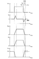
図15に、この種のトランジスタに電界効果型のトランジスタが用いられた場合の動作波形図を示す。駆動回路は、駆動電圧Vinをトランジスタのゲート電極に供給することによって、トランジスタのオン・オフを切替える。
まず、トランジスタがターンオンする過渡期に関して説明する。駆動電圧Vinがローからハイになると、トランジスタのゲート電極に向けて正のゲート電流Igが流れ、ゲート電極に電荷が蓄積される。ゲート電極に電荷が蓄積されると、トランジスタのゲート・ソース間電圧Vgsが上昇する。ゲート・ソース間電圧Vgsが上昇すると、トランジスタのドレインからソースに向けてドレイン電流Idが流れ始め、ドレイン・ソース間電圧Vdsが減少する。これらの過程を経て、トランジスタはオフからオンに移行する。
次に、トランジスタがターンオフする過渡期T100に関して説明する。駆動電圧Vinがハイからローになると、ゲート電極に蓄積していた電荷が放電し、ゲート電極から駆動回路に向けて負のゲート電流Igが流れ、ゲート・ソース間電圧Vgsが減少する。ゲート・ソース間電圧Vgsが減少すると、ドレイン電流Idも減少し、ドレイン・ソース間電圧Vdsが上昇する。これらの過程を経て、トランジスタはオンからオフに移行する。
FIG. 15 shows an operation waveform diagram when a field effect transistor is used as this type of transistor. The drive circuit switches the transistor on and off by supplying the drive voltage Vin to the gate electrode of the transistor.
First, the transition period in which the transistor is turned on will be described. When the drive voltage Vin changes from low to high, a positive gate current Ig flows toward the gate electrode of the transistor, and charges are accumulated in the gate electrode. When charges are accumulated in the gate electrode, the gate-source voltage Vgs of the transistor increases. When the gate-source voltage Vgs rises, the drain current Id starts to flow from the drain to the source of the transistor, and the drain-source voltage Vds decreases. Through these processes, the transistor shifts from off to on.
Next, the transition period T100 in which the transistor is turned off will be described. When the drive voltage Vin changes from high to low, the charge accumulated in the gate electrode is discharged, a negative gate current Ig flows from the gate electrode to the drive circuit, and the gate-source voltage Vgs decreases. When the gate-source voltage Vgs decreases, the drain current Id also decreases, and the drain-source voltage Vds increases. Through these processes, the transistor shifts from on to off.
図15に示すように、トランジスタがターンオフする過渡期T100の終盤では、ドレイン・ソース間電圧Vdsにサージ電圧が発生している。このサージ電圧は、急峻に変動するドレイン電流Idと回路中に寄生しているインダクタンスによって引き起こされる。
このサージ電圧の増大を抑えるためには、ドレイン電流Idを緩やかに変動させれば良い。例えば、トランジスタのゲート抵抗を大きくすれば、ゲート電極に蓄積していた電荷が放電する速度が減少し、負のゲート電流Igが緩やかに流れる。この結果、ドレイン電流Idも緩やかに減少し、サージ電圧の増大を抑えることができる。しかし、トランジスタのドレイン電流Idが緩やかに減少すると、トランジスタがターンオフするのに要する時間が増大し、ターンオフ損失が増大してしまう。即ち、この種のトランジスタには、ターンオフの過渡期T100において、サージ電圧とターンオフ損失の間にトレードオフ関係が存在する。
As shown in FIG. 15, a surge voltage is generated in the drain-source voltage Vds at the end of the transition period T100 when the transistor is turned off. This surge voltage is caused by a drain current Id that fluctuates rapidly and an inductance that is parasitic in the circuit.
In order to suppress the increase of the surge voltage, the drain current Id may be gradually changed. For example, if the gate resistance of the transistor is increased, the rate at which charges accumulated in the gate electrode are discharged decreases, and the negative gate current Ig flows gently. As a result, the drain current Id also decreases gradually, and an increase in surge voltage can be suppressed. However, when the drain current Id of the transistor is gradually reduced, the time required for the transistor to turn off increases, and the turn-off loss increases. That is, in this type of transistor, a trade-off relationship exists between the surge voltage and the turn-off loss in the turn-off transition period T100.
このトレードオフ関係を打破するためには、ターンオフの過渡期T100の序盤でドレイン電流Idを急峻に変動させ、過渡期T100の終盤でドレイン電流Idを緩慢に変動させるのが望ましい。過渡期T100の序盤でドレイン電流Idを急峻に変動させれば、ターンオフに要する時間を短縮することができる。この結果、ターンオフ損失を低く抑えることができる。また、過渡期T100の終盤でドレイン電流Idを緩慢に変動させれば、サージ電圧の増大を抑えることができる。 In order to break this trade-off relationship, it is desirable that the drain current Id is changed abruptly at the beginning of the turn-off transition period T100, and the drain current Id is changed slowly at the end of the transition period T100. If the drain current Id is abruptly changed at the beginning of the transition period T100, the time required for turn-off can be shortened. As a result, turn-off loss can be kept low. Further, if the drain current Id is slowly changed at the end of the transition period T100, an increase in surge voltage can be suppressed.
特許文献1には、バイポーラ型のトランジスタを駆動する回路が開示されている。なお、特許文献1の駆動回路に係る技術思想は、電界効果型のトランジスタを駆動する場合にも利用することができる。
特許文献1の駆動回路は、ゲート電極に接続している2つの抵抗体を備えている。この駆動回路によると、ターンオフの過渡期の序盤では、ゲート電極からの負のゲート電流が2つの抵抗体を介して流れる。一方、ターンオフの過渡期の終盤では、ゲート電極からの負のゲート電流が、一方の抵抗体が遮断されることによって他方の抵抗体のみを介して流れる。
The drive circuit of
特許文献1の駆動回路を利用すれば、ターンオフの過渡期の序盤で負のゲート電流を急峻に変動させることによって、ドレイン電流を急峻に変動させ、ターンオフに要する時間を短縮することができ得る。さらに、この駆動回路を利用すれば、ターンオフの過渡期の終盤で負のゲート電流を緩慢に変動させることによって、ドレイン電流を緩慢に変動させ、サージ電圧の増大を抑えることができ得る。
If the drive circuit of
特許文献1の駆動回路では、一方の抵抗体を遮断するタイミングが、回路中に組み込まれているコンデンサと抵抗体の時定数で予め設定されている。このため、特許文献1の駆動回路では、ターンオフが繰返し実行されると、一方の抵抗体を遮断するタイミングが、ターンオフの序盤と終盤を決定するタイミングから外れる事態が発生してしまう。予め設定されたタイミングで制御する手法は、トランジスタの動作に同調することができない。このため、特許文献1の駆動回路では、サージ電圧やターンオフ損失の増大を確実に抑えることができない。
本発明は、トランジスタが動作している状態を観測しながら、トランジスタのゲート抵抗の抵抗値を調整する技術を提供することを目的としている。なお、上記では、ターンオフする過渡期を中心に本発明の課題を説明してきたが、ターンオンする過渡期においても、トランジスタが動作している状態を観測しながらゲート抵抗の抵抗値を調整したい局面が多く存在する。本発明は、ターンオフとターンオンのいずれの過渡期においても有用な結果が得られる技術を提供する。
In the drive circuit of
An object of the present invention is to provide a technique for adjusting a resistance value of a gate resistance of a transistor while observing a state in which the transistor is operating. In the above description, the problem of the present invention has been described mainly in the transition period in which the transistor is turned off. However, there is an aspect in which the resistance value of the gate resistance is adjusted while observing the operating state of the transistor even in the transition period in which the transistor is turned on. There are many. The present invention provides a technique that can provide useful results in both the turn-off and turn-on transition periods.
本発明者らは、トランジスタのゲート電流に着目した。トランジスタのゲート電流は、ターンオン又はターンオフの過渡期において、その電流値の大きさが経時的に変動している。このため、トランジスタのゲート電流の電流値の大きさを指標にすれば、トランジスタが動作している状態を観測することができる。トランジスタのゲート電流の電流値の大きさを指標にすれば、トランジスタの動作に同調しながらゲート抵抗の抵抗値を調整することができる。
即ち、本発明は、トランジスタを駆動する回路に具現化することができる。本発明の駆動回路は、トランジスタのゲート電極に蓄積していた電荷が放電されるときのゲート電流の電流値に基づいて、そのトランジスタのゲート抵抗の抵抗値を調整する調整回路と、固定抵抗体とダイオードを介して前記トランジスタのゲート電極に電気的に接続している駆動電圧生成回路とを備えていることを特徴としている。調整回路は、ゲート電流の電流値の絶対値が大きいときにゲート抵抗の抵抗値を小さくし、ゲート電流の電流値の絶対値が小さいときにゲート抵抗の抵抗値を大きくする。ダイオードは、アノードが駆動電圧生成回路側に接続しており、カソードがトランジスタのゲート電極側に接続している。
駆動電圧生成回路からのオン電圧信号は、固定抵抗体でゲート電流に変換され、トランジスタのゲート電極に電荷を供給する。これにより、本発明の駆動回路は、トランジスタをオン状態に移行する。さらに、トランジスタがオフに移行するときに、トランジスタのゲート電極に蓄積していた電荷は、ダイオードによって固定抵抗体に流れる経路が遮断され、調整回路に向けて負のゲート電流として流れることができる。調整回路は、その負のゲート電流に基づいて、トランジスタのゲート抵抗の抵抗値を調整することができる。
この調整回路が設けられていると、トランジスタがターンオフする過渡期において、ゲート電流の電流値の絶対値が大きくなる序盤では、ゲート抵抗を小さくして電荷を素早く放電することができる。一方、ゲート電流の電流値の絶対値が小さくなる終盤では、ゲート抵抗を大きくして電荷をゆっくりと放電することができる。したがって、本発明の駆動回路は、ターンオフの過渡期の序盤において、トランジスタを流れるドレイン電流を急峻に変動させ、ターンオフに要する時間を短縮することができる。さらに、本発明の駆動回路は、ターンオフの過渡期の終盤において、トランジスタを流れるドレイン電流を緩慢に変動させ、サージ電圧の増大を抑えることができる。本発明の駆動回路によると、サージ電圧とターンオフ損失の間に存在するトレードオフ関係を打破することができる。
The inventors paid attention to the gate current of the transistor. The magnitude of the current value of the gate current of the transistor fluctuates with time during a turn-on or turn-off transition period. For this reason, if the magnitude of the current value of the gate current of the transistor is used as an index, the state in which the transistor is operating can be observed. If the magnitude of the current value of the gate current of the transistor is used as an index, the resistance value of the gate resistance can be adjusted while synchronizing with the operation of the transistor.
That is, the present invention can be embodied in a circuit for driving a transistor. The drive circuit of the present invention includes an adjustment circuit that adjusts the resistance value of the gate resistance of the transistor based on the current value of the gate current when the charge accumulated in the gate electrode of the transistor is discharged, and a fixed resistor And a drive voltage generation circuit electrically connected to the gate electrode of the transistor through a diode . The adjustment circuit decreases the resistance value of the gate resistance when the absolute value of the current value of the gate current is large, and increases the resistance value of the gate resistance when the absolute value of the current value of the gate current is small. The diode has an anode connected to the drive voltage generation circuit side and a cathode connected to the gate electrode side of the transistor.
An on-voltage signal from the drive voltage generation circuit is converted into a gate current by a fixed resistor, and charges are supplied to the gate electrode of the transistor. Thereby, the driving circuit of the present invention shifts the transistor to the on state. Furthermore, when the transistor is turned off, the charge accumulated in the gate electrode of the transistor is blocked by the diode through the path through the fixed resistor, and can flow as a negative gate current toward the adjustment circuit. The adjustment circuit can adjust the resistance value of the gate resistance of the transistor based on the negative gate current.
When this adjustment circuit is provided, the gate resistance can be reduced to quickly discharge the charge in the early stage when the absolute value of the current value of the gate current increases during the transition period in which the transistor is turned off. On the other hand, in the final stage when the absolute value of the gate current value is small, the gate resistance can be increased to discharge the charge slowly. Therefore, the driving circuit of the present invention can drastically change the drain current flowing through the transistor in the early stage of the turn-off transition period, and can shorten the time required for the turn-off. Furthermore, the drive circuit of the present invention can slowly increase the drain current flowing through the transistor at the end of the turn-off transition period, thereby suppressing an increase in surge voltage. According to the drive circuit of the present invention, the trade-off relationship existing between the surge voltage and the turn-off loss can be overcome.
本発明の調整回路は、設定されたゲート電流の閾値に基づいて、トランジスタのゲート抵抗の抵抗値を調整することが好ましい。
上記の調整回路では、ゲート電流の所定の電流値が閾値として設定されている。上記の調整回路では、その閾値に基づいてゲート抵抗の抵抗値を調整する。したがって、上記の調整回路を有する駆動回路は、ターンオフの過渡期の序盤と終盤を正確に区別してトランジスタを駆動させることができる。
The adjustment circuit of the present invention preferably adjusts the resistance value of the gate resistance of the transistor based on the set threshold value of the gate current.
In the above adjustment circuit, a predetermined current value of the gate current is set as the threshold value. In the above adjustment circuit, the resistance value of the gate resistance is adjusted based on the threshold value. Therefore, the drive circuit having the adjustment circuit can drive the transistor by accurately distinguishing between the beginning and end of the turn-off transition period.
本発明の駆動回路では、ダイオードとゲート抵抗を調整する調整回路が、トランジスタと同一の半導体基板内に形成されていることが好ましい。
In the driving circuit of the present invention, the adjustment circuit for adjusting the diode and the gate resistance is not preferable to be formed on the same semiconductor substrate and a transistor.
本発明の調整回路は、調整用トランジスタと、その調整用トランジスタのオン抵抗よりも抵抗値が大きい抵抗体を有しているのが好ましい。その抵抗体は、調整用トランジスタのゲート電極と入力電極の間に設けられているとともに、その一端がトランジスタのゲート電極に接続している。このため、調整用トランジスタは、抵抗体の両端に発生する電圧差によってオン・オフする。トランジスタのゲート電流は、電流値の絶対値が大きいときに調整用トランジスタがオンすることによって調整用トランジスタを通過し、電流値の絶対値が小さいときに調整用トランジスタがオフすることによって抵抗体を通過する。
上記の駆動回路によると、トランジスタがターンオフする過渡期において、ゲート電流の電流値の絶対値が大きくなる序盤では、抵抗体の両端に発生する電圧差によって調整用トランジスタがオンし、ゲート電流が調整用トランジスタを介して流れる。調整用トランジスタのオン抵抗は小さいので、トランジスタのゲート電極に蓄積していた電荷を素早く放電することができる。一方、ゲート電流の電流値の絶対値が小さくなる終盤では、抵抗体の両端に発生する電圧差が小さくなり調整用トランジスタがオフし、ゲート電流が抵抗体を介して流れる。抵抗体の抵抗値は大きいので、トランジスタのゲート電極に蓄積していた電荷をゆっくりと放電することができる。この結果、本発明の駆動回路によると、サージ電圧とターンオフ損失の間に存在するトレードオフ関係を打破することができる。
The adjustment circuit of the present invention preferably includes an adjustment transistor and a resistor having a resistance value larger than the on-resistance of the adjustment transistor. The resistor is provided between the gate electrode and the input electrode of the adjustment transistor, and one end of the resistor is connected to the gate electrode of the transistor. For this reason, the adjustment transistor is turned on / off by a voltage difference generated between both ends of the resistor. The gate current of the transistor passes through the adjusting transistor when the adjusting transistor is turned on when the absolute value of the current value is large, and turns off the resistor when the adjusting transistor is turned off when the absolute value of the current value is small. pass.
According to the above drive circuit, in the early period when the absolute value of the current value of the gate current increases during the transition period when the transistor turns off, the adjustment transistor is turned on by the voltage difference generated across the resistor, and the gate current is adjusted. Flows through the transistor. Since the on-resistance of the adjustment transistor is small, the charge accumulated in the gate electrode of the transistor can be quickly discharged. On the other hand, in the final stage when the absolute value of the current value of the gate current becomes small, the voltage difference generated at both ends of the resistor becomes small, the adjustment transistor is turned off, and the gate current flows through the resistor. Since the resistance value of the resistor is large, the charge accumulated in the gate electrode of the transistor can be discharged slowly. As a result, according to the drive circuit of the present invention, the trade-off relationship existing between the surge voltage and the turn-off loss can be broken.
本発明の調整用トランジスタは、p型の電界効果型トランジスタであってもよい。この場合、調整用トランジスタのソース電極が、抵抗体の一端とトランジスタのゲート電極の間に接続している。さらに、調整用トランジスタのドレイン電極が、接地している。 The adjustment transistor of the present invention may be a p-type field effect transistor. In this case, the source electrode of the adjustment transistor is connected between one end of the resistor and the gate electrode of the transistor. Further, the drain electrode of the adjustment transistor is grounded.
本発明の調整用トランジスタは、n型の電界効果型トランジスタであってもよい。この場合、調整用トランジスタのゲート電極及びドレイン電極が、抵抗体の一端とトランジスタのゲート電極の間に接続している。 The adjusting transistor of the present invention may be an n-type field effect transistor. In this case, the gate electrode and the drain electrode of the adjustment transistor are connected between one end of the resistor and the gate electrode of the transistor.
本発明の駆動回路は、トランジスタの動作の状態を良好に反映しているゲート電流に基づいてトランジスタのゲート抵抗の抵抗値を調整する。このため、本発明の駆動回路は、トランジスタの動作に同調してゲート抵抗の抵抗値を調整することができる。 The drive circuit of the present invention adjusts the resistance value of the gate resistance of the transistor based on the gate current that well reflects the state of operation of the transistor. For this reason, the drive circuit of the present invention can adjust the resistance value of the gate resistor in synchronization with the operation of the transistor.
本発明の好ましい形態を列記する。
(第1形態) 本発明の駆動回路は、電界効果型のトランジスタを駆動する。
(第2形態) 調整用トランジスタは、p型のMOSFETである。この場合、p-MOSFETのソース電極とゲート電極の間には、p-MOSFETのオン抵抗よりも抵抗値が大きい抵抗体が設けられている。さらに、p-MOSFETのソース電極はトランジスタのゲート電極に接続しており、p-MOSFETのドレイン電極は接地しており、p-MOSFETのゲート電極は駆動電圧生成回路に接続している。
(第3形態) 調整用トランジスタは、n型のMOSFETである。この場合、n-MOSFETのソース電極とゲート電極の間には、n-MOSFETのオン抵抗よりも抵抗値が大きい抵抗体が設けられている。さらに、n-MOSFETのゲート電極とドレイン電極はトランジスタのゲート電極に接続しており、n-MOSFETのソース電極は駆動電圧生成回路に接続している。
Preferred forms of the present invention are listed.
First Embodiment A driving circuit of the present invention drives a field effect transistor.
(Second Embodiment) The adjustment transistor is a p-type MOSFET. In this case, a resistor having a resistance value larger than the on-resistance of the p-MOSFET is provided between the source electrode and the gate electrode of the p-MOSFET. Furthermore, the source electrode of the p-MOSFET is connected to the gate electrode of the transistor, the drain electrode of the p-MOSFET is grounded, and the gate electrode of the p-MOSFET is connected to the drive voltage generation circuit.
(Third Embodiment) The adjustment transistor is an n-type MOSFET. In this case, a resistor having a resistance value larger than the on-resistance of the n-MOSFET is provided between the source electrode and the gate electrode of the n-MOSFET. Furthermore, the gate electrode and drain electrode of the n-MOSFET are connected to the gate electrode of the transistor, and the source electrode of the n-MOSFET is connected to the drive voltage generation circuit.
図1に、電界効果型のトランジスタ30を駆動するための駆動回路10の回路図を示す。トランジスタ30は、負荷40とグランド(GND)の間に接続されている。トランジスタ30と負荷40の間には、配線等の寄生インダクタンスが接続されている。駆動回路10は、矩形波の駆動電圧Vinをトランジスタ30のゲート電極Gに供給し、その駆動電圧Vinに基づいてトランジスタ30のオン・オフを切替える。駆動回路10は、トランジスタ30のオン・オフを切替えることによって、電圧供給源50の直流電圧Vddを負荷40に供給する状態と供給しない状態を切替える。
FIG. 1 shows a circuit diagram of a
駆動回路10は、駆動電圧生成回路12と、第3抵抗体Rg3(固定抵抗体の一例)と、ダイオードD20と、調整回路20を備えている。駆動電圧生成回路12は、第3抵抗体Rg3とダイオードD20を介してトランジスタ30のゲート電極Gに電気的に接続している。ダイオードD20のアノードは、駆動電圧生成回路12側に接続しており、カソードはトランジスタ30のゲート電極G側に接続している。ダイオードD20と調整回路20は、駆動電圧生成回路12とトランジスタ30の間に、並列回路を構成している。調整回路20は、ゲート電流検出手段22と、スイッチ手段SWと、第1抵抗体Rg1と、第2抵抗体Rg2と第2のダイオードD22を備えている。第1抵抗体Rg1の抵抗値は、第2抵抗体Rg2の抵抗値よりも小さい。第2ダイオードD22のアノードはトランジスタ30のゲート電極G側に接続しており、カソードは駆動電圧生成回路12側に接続している。
The
ゲート電流検出手段22は、トランジスタ30のゲート電極Gに蓄積していた電荷が放電するときの負のゲート電流Ig(-)を検出し、その負のゲート電流Ig(-)の電流値に基づいてスイッチ手段SWの開閉を切替える。ゲート電流検出手段22は、負のゲート電流Ig(-)の電流値の絶対値が大きいときにスイッチ手段SWを閉鎖し、負のゲート電流Ig(-)の電流値の絶対値が小さいときにスイッチ手段SWを開放する。
The gate current detection means 22 detects the negative gate current Ig (−) when the charge accumulated in the gate electrode G of the
図2に、トランジスタ30の動作波形図を示す。
まず、トランジスタ30がターンオンする過渡期に関して説明する。駆動電圧Vinがローからハイになると、駆動電圧Vinは、第3抵抗体Rg3で正のゲート電流Ig(+)に変換される。正のゲート電流Ig(+)は、第2ダイオードD22が逆方向に設けられているので、ダイオードD20を介してトランジスタ30のゲート電極Gに供給される。トランジスタ30のゲート電極Gに正のゲート電流Ig(+)が供給されると、ゲート電極Gに電荷が蓄積される。ゲート電極Gに電荷が蓄積されると、トランジスタ30のゲート・ソース間電圧Vgsが上昇する。ゲート・ソース間電圧Vgsが上昇すると、トランジスタ30のドレイン電極DからソースSに向けてドレイン電流Idが流れ始め、ドレイン・ソース間電圧Vdsが減少する。これらの過程を経て、トランジスタ30はオフからオンに移行する。
FIG. 2 shows an operation waveform diagram of the
First, a transition period in which the
次に、トランジスタ30がターンオフする過渡期T10に関して説明する。駆動電圧Vinがハイからローになると、ゲート電極Gに蓄積していた電荷が放電する。電荷の放電に伴う負のゲート電流Ig(-)は、ダイオードD20が設けられているので、ゲート電流検出手段22に向けて流れる。負のゲート電流Ig(-)の電流値の絶対値は、ターンオフした過渡期T10の序盤T12において徐々に増大する。ゲート電流検出手段22は、負のゲート電流Ig(-)の電流値の絶対値を検出し、その絶対値が所定の閾値を越えると(電流値が閾値を下回ると)スイッチ手段SWを閉鎖する。このため、負のゲート電流Ig(-)は、抵抗値の小さい第1抵抗体Rg1を介してグランドGNDに流れる。スイッチ手段SWが閉鎖すると、トランジスタ30がターンオフする過渡期T10の序盤T12において、負のゲート電流Ig(-)は、その電流値の絶対値が急激に大きくなるように挙動する。このため、調整回路20は、ターンオフの過渡期T10の序盤T12において、トランジスタ30のゲート電極Gから電荷を素早く放電するように働く。この結果、ターンオフの過渡期T10の序盤T12でターンオフに要する時間を短縮することができる。場合によっては、図2に示すように、従来の駆動回路の過渡期T100に比して、トランジスタ30がターンオフに要する過渡期T10の時間が短縮される。
なお、負のゲート電流Ig(-)の電流値の絶対値が所定の閾値を超えるまでは、スイッチ手段SWが開放しており、ゲート抵抗の抵抗値は高く、電荷はゆっくりと放電する。しかし、この期間は極めて短く、ターンオフに要する時間を実質的に長期化するものではない。
Next, the transition period T10 in which the
Note that, until the absolute value of the negative gate current Ig (−) exceeds the predetermined threshold, the switch means SW is open, the resistance value of the gate resistance is high, and the charge is slowly discharged. However, this period is extremely short and does not substantially increase the time required for turn-off.
ターンオフの過渡期T10の終盤T14になると、負のゲート電流Ig(-)の電流値が徐々に減少する。ゲート電流検出手段22は、負のゲート電流Ig(-)の電流値の絶対値を検出し、その絶対値が所定の閾値を下回ると(電流値が所定の閾値を上回ると)スイッチ手段SWを開放する。このため、負のゲート電流Ig(-)は、抵抗値の大きな第2抵抗体Rg2、第3抵抗体Rg3及び駆動電圧生成回路12を介してグランドGNDに流れる。スイッチ手段SWが開放すると、トランジスタ30がターンオフする過渡期T10の終盤T14において、負のゲート電流Ig(-)は、その電流値の絶対値が小さくなるように挙動する。このため、調整回路20は、ターンオフの過渡期T10の終盤T14において、トランジスタ30のゲート電極Gから電荷をゆっくりと放電するように働く。この結果、トランジスタ30のドレイン電流Idが緩慢に流れ、サージ電圧の増大を抑えることができる。
駆動回路10によると、トランジスタ30がターンオフする過渡期T10において、サージ電圧とターンオフ損失の間に存在するトレードオフ関係を打破することができる。
At the end T14 of the turn-off transition period T10, the current value of the negative gate current Ig (−) gradually decreases. The gate current detection means 22 detects the absolute value of the current value of the negative gate current Ig (−), and when the absolute value falls below a predetermined threshold value (when the current value exceeds a predetermined threshold value), the switch means SW Open. Therefore, the negative gate current Ig (−) flows to the ground GND through the second resistor Rg2, the third resistor Rg3, and the drive
According to the
また、本実施例の駆動回路10は、ゲート電流Igを観測している点に特徴を有する。一般的に、電圧供給源50とトランジスタ30の間には、複数の負荷が接続されていることが多い。このため、ある負荷で大電流が流れると電圧供給源50の直流電圧Vddが低下する。特に、自動車の分野では、バッテリーに十分な電流容量がないので、電圧供給源50の直流電圧Vddは変動し易い。
例えば、トランジスタ30のドレイン電圧を観測して、ゲート抵抗を調整することも考えられる。しかし、トランジスタ30のドレイン電圧を観測する場合、電圧供給源50の直流電圧Vddが変動することによって、トランジスタ30のドレイン電圧も変動してしまう。このため、トランジスタがターンオフする過渡期の終盤のタイミングを性格に把握できない。
一方、本実施例の駆動回路10のようにゲート電流Igを観測する場合は、電圧供給源50の直流電圧Vddが変動したとしても、ゲート電流Igはその影響を受けないので、トランジスタがターンオフする過渡期の終盤のタイミングを性格に把握することができる。
Further, the
For example, it is conceivable to adjust the gate resistance by observing the drain voltage of the
On the other hand, when the gate current Ig is observed as in the driving
以下、具体的な回路の構成を示す。なお、同一の構成要素に関しては同一符号を付し、その説明を省略する。
図3に、図1のゲート電流検出手段22とスイッチ手段SWと第1抵抗体Rg1が、p型のMOSFET(Metal Oxide Semiconductor Field Effect Transistor)24で実現されている例を示す。p-MOSFET24の閾値電圧とスイッチ動作が、図1のゲート電流検出手段22とスイッチ手段SWに等価である。p-MOSFET24のオン抵抗が、第1抵抗体Rg1と等価である。
A specific circuit configuration will be described below. In addition, the same code | symbol is attached | subjected about the same component and the description is abbreviate | omitted.
FIG. 3 shows an example in which the gate current detecting
第2抵抗体Rg2は、p-MOSFET24のゲート電極Gとソース電極S(入力電極の一例)の間に設けられている。このため、p-MOSFET24は、第2抵抗体Rg2の両端に発生する電圧差によってオン・オフする。さらに、第2抵抗体Rg2の一端は、トランジスタ30のゲート電極Gに接続しているとともに、他端が第3抵抗体Rg3及び駆動電圧生成回路12を介してグランドGNDに接続している。p-MOSFET24のドレイン電極Dは、グランドGNDに接続している。
The second resistor Rg2 is provided between the gate electrode G and the source electrode S (an example of an input electrode) of the p-
この駆動回路10によると、トランジスタ30がターンオフする過渡期において、負のゲート電流Ig(-)の電流値の絶対値が大きくなる序盤では、第2抵抗体Rg2の両端に発生する電圧差によってp-MOSFET24がオンする。p-MOSFET24がオンすると、負のゲート電流Ig(-)は、p-MOSFET24のソース電極Sからドレイン電極Dを通過してグランドGNDに流れる。p-MOSFET24のオン抵抗は小さいので、トランジスタ30のゲート電極Gに蓄積していた電荷は、素早く放電することができる。この結果、トランジスタ30がターンオフするのに要する時間を短縮することができる。
一方、負のゲート電流Ig(-)の電流値の絶対値が小さくなる終盤では、第2抵抗体Rg2の両端に発生する電圧差が小さくなりp-MOSFET24がオフする。p-MOSFET24がオフすると、負のゲート電流Ig(-)は、第2抵抗体Rg2、第3抵抗体Rg3及び駆動電圧生成回路12を介してグランドGNDに流れる。第2抵抗体Rg2の抵抗値は大きいので、トランジスタ30のゲート電極Gに蓄積していた電荷は、ゆっくりと放電することができる。この結果、サージ電圧の増大を抑えることができる。
According to this
On the other hand, at the final stage when the absolute value of the negative gate current Ig (−) becomes small, the voltage difference generated at both ends of the second resistor Rg2 becomes small and the p-
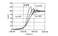
図4に、トランジスタ30をターンオフした過渡期のドレイン・ソース間電圧Vdsの変動を示す。「pMOSあり」が図3の駆動回路10の結果である。ここで、「未対策」は、図1の第1抵抗体Rg1のみが設けられた場合の結果である。また、「pMOSなし」は、図3の第2抵抗体Rg2のみが設けられた結果である。なお、第1抵抗体Rg1の抵抗値は0.1Ωであり、第2抵抗体Rg2の抵抗値は30Ωであり、第3抵抗体Rg3の抵抗値は3Ωである。また、p-MOSFET24の閾値電圧Vthは、−2.7Vである。
図4に示すように、未対策の場合は、電荷の放電する速度が大きく、大きなサージ電圧が発生している。一方、「pMOSあり」及び「pMOSなし」の場合は、電荷の放電する速度が小さく抑えられ、サージ電圧の増大が抑制されている。しかし、「pMOSなし」の場合は、ターンオフに要する時間が長くなっており、ターンオフ損失が増大してしまう。
FIG. 4 shows the fluctuation of the drain-source voltage Vds in the transition period when the
As shown in FIG. 4, when no countermeasure is taken, the charge discharge rate is high and a large surge voltage is generated. On the other hand, in the case of “with pMOS” and “without pMOS”, the discharge rate of electric charges is suppressed to be small, and an increase in surge voltage is suppressed. However, in the case of “without pMOS”, the time required for turn-off becomes longer, and the turn-off loss increases.
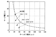
図5に、サージ電圧とターンオフ損失の関係を示す。
「pMOSなし」の場合は、「未対策」の場合に比してサージ電圧が抑制されているものの、ターンオフに要する時間が長くなっており、ターンオフ損失が増大している。「pMOSなし」の結果は、トレードオフ曲線から大きく改善されていると評価できない。
一方、「pMOSあり」の場合は、「未対策」の場合に比してターンオフ損失をほとんど増大させることなく、サージ電圧を顕著に低減している。「pMOSあり」の結果は、トレードオフ曲線から大きく改善されていると評価できる。
FIG. 5 shows the relationship between surge voltage and turn-off loss.
In the case of “no pMOS”, the surge voltage is suppressed as compared with the case of “unmeasured”, but the time required for turn-off is longer and the turn-off loss is increased. The result of “no pMOS” cannot be evaluated as greatly improved from the trade-off curve.
On the other hand, in the case of “with pMOS”, the surge voltage is significantly reduced without substantially increasing the turn-off loss as compared with the case of “unmeasured”. The result of “with pMOS” can be evaluated as greatly improved from the trade-off curve.
図6に、第2抵抗体Rg2の抵抗値を3Ω、10Ω、30Ωと変えたときのドレイン・ソース間電圧Vdsの変動を示す。
第2抵抗体Rg2の抵抗値を大きくするほど、過渡期の終盤において電荷の放電する速度が抑えられ、サージ電圧の増大を抑制することができる。
FIG. 6 shows the fluctuation of the drain-source voltage Vds when the resistance value of the second resistor Rg2 is changed to 3Ω, 10Ω, and 30Ω.
As the resistance value of the second resistor Rg2 is increased, the rate at which charges are discharged at the end of the transition period is suppressed, and an increase in surge voltage can be suppressed.
図7に、第2抵抗体Rg2の抵抗値を3Ω、10Ω、30Ωに変えたときのサージ電圧とターンオフ損失の間の関係を示す。
第2抵抗体の抵抗値を大きくするほど、サージ電圧とターンオフ損失の間に存在するトレードオフ関係を打破することができる。
FIG. 7 shows the relationship between the surge voltage and the turn-off loss when the resistance value of the second resistor Rg2 is changed to 3Ω, 10Ω, and 30Ω.
As the resistance value of the second resistor is increased, the trade-off relationship existing between the surge voltage and the turn-off loss can be broken.
図8に、p-MOSFET24の閾値電圧Vthを-1.7V、-2.7V、-3.7Vに変えたときのドレイン・ソース間電圧Vdsの変動を示す。
p-MOSFET24の閾値電圧Vthの絶対値が小さいほど、p-MOSFET24を介した電荷の放電が長く確保されるので、ターンオフに要する時間が短くなっている。さらに、ターンオフの過渡期の終盤では、第2抵抗Rg2を介した電荷の放電が行われるので、サージ電圧のサージ電圧の増大を抑制することができる。
FIG. 8 shows fluctuations in the drain-source voltage Vds when the threshold voltage Vth of the p-
The smaller the absolute value of the threshold voltage Vth of the p-
図9に、p-MOSFET24の閾値電圧Vthを-1.7V、-2.7V、-3.7Vに変えたときのサージ電圧とターンオフ損失の間の関係を示す。
p-MOSFET24の閾値電圧Vthを調整する場合はいずれも、サージ電圧とターンオフ損失の間に存在するトレードオフ関係を打破することができる。
FIG. 9 shows the relationship between the surge voltage and the turn-off loss when the threshold voltage Vth of the p-
In any case where the threshold voltage Vth of the p-
図10に、図1のゲート電流検出手段22とスイッチ手段SWと第1抵抗体Rg1が、n型のMOSFET26で実現されている例を示す。n-MOSFET26の閾値電圧とスイッチ動作が、図1のゲート電流検出手段22とスイッチ手段SWに等価である。n-MOSFET26のオン抵抗が、第1抵抗体Rg1と等価である。
FIG. 10 shows an example in which the gate current detecting
第2抵抗体Rg2は、n-MOSFET26のゲート電極Gとソース電極S(入力電極の一例)の間に設けられている。このため、n-MOSFET26は、第2抵抗体Rg2の両端に発生する電圧差によってオン・オフする。さらに、第2抵抗体Rg2の一端は、トランジスタ30のゲート電極Gに接続しているとともに、他端が第2のダイオードD22、第3抵抗体Rg3及び駆動電圧生成回路12を介してグランドに接続している。n-MOSFET26のゲート電極Gとドレイン電極Dは、第2抵抗体Rg2の一端とトランジスタ30のゲート電極Gの間に接続している。第2のダイオードD22は、駆動電圧生成回路12とn-MOSFET26のソース電極Sの間に設けられている。
The second resistor Rg2 is provided between the gate electrode G and the source electrode S (an example of an input electrode) of the n-
この駆動回路10によると、トランジスタ30がターンオフする過渡期において、負のゲート電流Ig(-)の電流値の絶対値が大きくなる序盤では、第2抵抗体Rg2の両端に発生する電圧差によってn-MOSFET26がオンする。n-MOSFET26がオンすると、負のゲート電流Ig(-)は、n-MOSFET26のドレイン電極Dからソース電極Sを通過して、さらに第2のダイオードD22、第3抵抗体Rg3及び駆動電圧生成回路12を介してグランドGNDに流れる。即ち、負のゲート電流Ig(-)は、第2抵抗体Rg2を迂回して流れる。n-MOSFET26のオン抵抗は小さいので、トランジスタ30のゲート電極Gに蓄積していた電荷は、素早く放電することができる。この結果、トランジスタ30がターンオフするのに要する時間を短縮することができる。
一方、負のゲート電流Ig(-)の電流値の絶対値が小さくなる終盤では、第2抵抗体Rg2の両端に発生する電圧差が小さくなりn-MOSFET26がオフする。n-MOSFET26がオフすると、負のゲート電流Ig(-)は、第2抵抗体Rg2を通過して、さらに第2のダイオードD22、第3抵抗体Rg3及び駆動電圧生成回路12を介してグランドGNDに流れる。第2抵抗体Rg2の抵抗値は大きいので、トランジスタ30のゲート電極Gに蓄積していた電荷は、ゆっくりと放電することができる。この結果、サージ電圧の増大を抑えることができる。
According to this
On the other hand, at the final stage when the absolute value of the negative gate current Ig (−) becomes small, the voltage difference generated at both ends of the second resistor Rg2 becomes small and the n−
図11に、第2抵抗体Rg2の抵抗値を3Ω、10Ω、30Ωに変えたときのドレイン・ソース間電圧Vdsの変動を示す。ここで、n-MOSFET26の閾値電圧Vthは、1.1Vである。
第2抵抗体Rg2の抵抗値を大きくするほど、過渡期の終盤において電荷の放電する速度が抑えられ、サージ電圧の増大を抑制することができる。
FIG. 11 shows the fluctuation of the drain-source voltage Vds when the resistance value of the second resistor Rg2 is changed to 3Ω, 10Ω, and 30Ω. Here, the threshold voltage Vth of the n-
As the resistance value of the second resistor Rg2 is increased, the rate at which charges are discharged at the end of the transition period is suppressed, and an increase in surge voltage can be suppressed.
図12に、第2抵抗体Rg2の抵抗値を3Ω、10Ω、30Ωに変えたときのサージ電圧とターンオフ損失の間の関係を示す。
第2抵抗体の抵抗値を大きくするほど、サージ電圧とターンオフ損失の間に存在するトレードオフ関係を打破することができる。
FIG. 12 shows the relationship between the surge voltage and the turn-off loss when the resistance value of the second resistor Rg2 is changed to 3Ω, 10Ω, and 30Ω.
As the resistance value of the second resistor is increased, the trade-off relationship existing between the surge voltage and the turn-off loss can be broken.
図13に、n-MOSFET26の閾値電圧Vthを0.1V、1.1V、2.1Vに変えたときのドレイン・ソース間電圧Vdsの変動を示す。
n-MOSFET26の閾値電圧Vthが小さいほど、n-MOSFET26を介した電荷の放電が長く確保されるので、ターンオフに要する時間が短くなっている。さらに、ターンオフの過渡期の終盤では、第2抵抗Rg2を介した電荷の放電が行われるので、サージ電圧のサージ電圧の増大を抑制することができる。
FIG. 13 shows fluctuations in the drain-source voltage Vds when the threshold voltage Vth of the n-
The smaller the threshold voltage Vth of the n-
図14に、n-MOSFET26の閾値を0.1V、1.1V、2.1Vに変えたときのサージ電圧とターンオフ損失の間の関係を示す。
n-MOSFET26の閾値電圧Vthを調整する場合はいずれも、サージ電圧とターンオフ損失の間に存在するトレードオフ関係を打破することができる。
FIG. 14 shows the relationship between the surge voltage and the turn-off loss when the threshold value of the n-
In any case where the threshold voltage Vth of the n-
以上、本発明の具体例を詳細に説明したが、これらは例示に過ぎず、特許請求の範囲を限定するものではない。特許請求の範囲に記載の技術には、以上に例示した具体例を様々に変形、変更したものが含まれる。
また、本明細書または図面に説明した技術要素は、単独であるいは各種の組合せによって技術的有用性を発揮するものであり、出願時請求項記載の組合せに限定されるものではない。また、本明細書または図面に例示した技術は複数目的を同時に達成し得るものであり、そのうちの一つの目的を達成すること自体で技術的有用性を持つものである。
Specific examples of the present invention have been described in detail above, but these are merely examples and do not limit the scope of the claims. The technology described in the claims includes various modifications and changes of the specific examples illustrated above.
The technical elements described in this specification or the drawings exhibit technical usefulness alone or in various combinations, and are not limited to the combinations described in the claims at the time of filing. In addition, the technology exemplified in this specification or the drawings can achieve a plurality of objects at the same time, and has technical usefulness by achieving one of the objects.
10:駆動回路
12:駆動電圧生成回路
20:調整回路
22:ゲート電流検出手段
24:n-MOSFET
26:p-MOSFET
30:トランジスタ
40:負荷
50:電圧供給源
D20、D22:ダイオード
Rg1、Rg2、Rg3:抵抗体
SW:スイッチ手段
10: drive circuit 12: drive voltage generation circuit 20: adjustment circuit 22: gate current detection means 24: n-MOSFET
26: p-MOSFET
30: Transistor 40: Load 50: Voltage supply source D20, D22: Diode
Rg1, Rg2, Rg3: Resistors
SW: Switch means
Claims (6)
前記トランジスタのゲート電極に蓄積していた電荷が放電されるときのゲート電流の電流値に基づいて、前記トランジスタのゲート抵抗の抵抗値を調整する調整回路と、
固定抵抗体とダイオードを介して前記トランジスタのゲート電極に電気的に接続している駆動電圧生成回路と、を備えており、
前記調整回路は、前記ゲート電流の電流値の絶対値が大きいときに前記ゲート抵抗の抵抗値を小さくし、前記ゲート電流の電流値の絶対値が小さいときに前記ゲート抵抗の抵抗値を大きくしており、
前記ダイオードは、アノードが前記駆動電圧生成回路側に接続しており、カソードが前記トランジスタのゲート電極側に接続している駆動回路。 A circuit for driving a transistor,
An adjustment circuit based on the current value of the gate current, adjusting the resistance value of the gate resistance of the transistor when charges accumulated in the gate electrode of the transistor is discharged,
A driving voltage generating circuit electrically connected to the gate electrode of the transistor through a fixed resistor and a diode , and
The adjustment circuit reduces the resistance value of the gate resistance when the absolute value of the current value of the gate current is large, and increases the resistance value of the gate resistance when the absolute value of the current value of the gate current is small. And
The diode has a drive circuit in which an anode is connected to the drive voltage generation circuit side and a cathode is connected to the gate electrode side of the transistor .
前記抵抗体は、前記調整用トランジスタのゲート電極と入力電極の間に設けられているとともに、その一端が前記トランジスタのゲート電極に接続しており、
前記調整用トランジスタは、前記抵抗体の両端に発生する電圧差によってオン・オフし、
前記ゲート電流は、電流値の絶対値が大きいときに前記調整用トランジスタがオンすることによって前記調整用トランジスタを通過し、電流値の絶対値が小さいときに前記調整用トランジスタがオフすることによって前記抵抗体を通過することを特徴とする請求項1〜3のいずれか一項に記載の駆動回路。 The adjustment circuit includes an adjustment transistor and a resistor having a resistance value larger than the on-resistance of the adjustment transistor.
The resistor, together is provided between the gate electrode and the input electrode of said regulating transistor has its one end connected to the gate electrode of said transistor,
The adjustment transistor is turned on and off by a voltage difference generated between both ends of the resistor,
The gate current, said by the adjustment transistor when the absolute value of the current value passed through the adjustment transistor by turning on the adjustment transistor when the absolute value is small in the current value is turned off The drive circuit according to claim 1, wherein the drive circuit passes through a resistor.
前記調整用トランジスタのソース電極が、前記抵抗体の一端と前記トランジスタのゲート電極の間に接続しており、
前記調整用トランジスタのドレイン電極が、接地電位に固定されていることを特徴とする請求項4の駆動回路。 The adjusting transistor is a p-type field effect transistor;
The source electrode of the adjustment transistors, are connected between the gate electrode of the one end and the transistors of the resistor,
5. The drive circuit according to claim 4 , wherein a drain electrode of the adjustment transistor is fixed to a ground potential.
前記調整用トランジスタのゲート電極及びドレイン電極が、前記抵抗体の一端と前記トランジスタのゲート電極の間に接続していることを特徴とする請求項4の駆動回路。
The adjusting transistor is an n-type field effect transistor;
Driving circuit according to claim 4 in which the gate electrode and the drain electrode, characterized in that connected between the gate electrode of the one end and the transistors of the resistor of the adjustment transistor.
Priority Applications (8)
| Application Number | Priority Date | Filing Date | Title |
|---|---|---|---|
| JP2006204769A JP4807577B2 (en) | 2006-07-27 | 2006-07-27 | Transistor drive circuit |
| DE102007063687A DE102007063687B4 (en) | 2006-03-22 | 2007-03-22 | Circuit with a transistor |
| DE102007063721.9A DE102007063721B4 (en) | 2006-03-22 | 2007-03-22 | Circuit having a transistor and a drive circuit for driving the transistor |
| US11/723,967 US7671636B2 (en) | 2006-03-22 | 2007-03-22 | Switching circuit and driving circuit for transistor |
| DE102007013824A DE102007013824B4 (en) | 2006-03-22 | 2007-03-22 | Circuit with a transistor |
| US12/654,323 US7982508B2 (en) | 2006-03-22 | 2009-12-17 | Switching circuit and driving circuit for transistor |
| US13/105,021 US8179169B2 (en) | 2006-03-22 | 2011-05-11 | Driving circuit with variable resistor for transistor |
| US13/433,624 US8519748B2 (en) | 2006-03-22 | 2012-03-29 | Driving circuit for driving transistor based on control current |
Applications Claiming Priority (1)
| Application Number | Priority Date | Filing Date | Title |
|---|---|---|---|
| JP2006204769A JP4807577B2 (en) | 2006-07-27 | 2006-07-27 | Transistor drive circuit |
Publications (2)
| Publication Number | Publication Date |
|---|---|
| JP2008035068A JP2008035068A (en) | 2008-02-14 |
| JP4807577B2 true JP4807577B2 (en) | 2011-11-02 |
Family
ID=39124061
Family Applications (1)
| Application Number | Title | Priority Date | Filing Date |
|---|---|---|---|
| JP2006204769A Expired - Fee Related JP4807577B2 (en) | 2006-03-22 | 2006-07-27 | Transistor drive circuit |
Country Status (1)
| Country | Link |
|---|---|
| JP (1) | JP4807577B2 (en) |
Families Citing this family (5)
| Publication number | Priority date | Publication date | Assignee | Title |
|---|---|---|---|---|
| KR100967781B1 (en) | 2008-04-10 | 2010-07-05 | 엘에스산전 주식회사 | Circuit for driving switching device in inverter |
| KR101533298B1 (en) * | 2008-09-23 | 2015-07-09 | 엘지이노텍 주식회사 | Apparatus for supplying power |
| JP6451429B2 (en) | 2015-03-16 | 2019-01-16 | 株式会社デンソー | Driving device for switching element |
| JP7068993B2 (en) * | 2018-11-21 | 2022-05-17 | 三菱電機株式会社 | Simulation circuit and simulation method |
| US11558054B1 (en) * | 2021-11-15 | 2023-01-17 | Kabushiki Kaisha Toshiba | Active gate driving signal optimization |
Family Cites Families (5)
| Publication number | Priority date | Publication date | Assignee | Title |
|---|---|---|---|---|
| JPH05235722A (en) * | 1992-02-19 | 1993-09-10 | Energy Support Corp | Switching element drive circuit |
| JPH05336732A (en) * | 1992-06-02 | 1993-12-17 | Toshiba Corp | Igbt gate circuit |
| JP3664061B2 (en) * | 1999-12-28 | 2005-06-22 | 日産自動車株式会社 | Current control type drive circuit for semiconductor device |
| JP2001274665A (en) * | 2000-03-27 | 2001-10-05 | Nissan Motor Co Ltd | Drive method and drive circuit for voltage drive element |
| JP4223379B2 (en) * | 2003-12-10 | 2009-02-12 | 三菱電機株式会社 | Switching device control device and motor drive circuit control device |
-
2006
- 2006-07-27 JP JP2006204769A patent/JP4807577B2/en not_active Expired - Fee Related
Also Published As
| Publication number | Publication date |
|---|---|
| JP2008035068A (en) | 2008-02-14 |
Similar Documents
| Publication | Publication Date | Title |
|---|---|---|
| CN106357251B (en) | Semiconductor switch device | |
| US8390341B2 (en) | Output circuit | |
| CN109417386B (en) | Drive circuit and power module using same | |
| US9444444B2 (en) | Anti-ringing technique for switching power stage | |
| CN107302351B (en) | Driving device and inductive load driving device | |
| JP5545308B2 (en) | Driving circuit | |
| JP2011211836A (en) | Switching device driving unit and semiconductor apparatus | |
| US9584115B2 (en) | Duty cycle-controlled load switch | |
| JP2010130822A (en) | Semiconductor device | |
| CN107078733B (en) | Driving circuit | |
| US10469068B1 (en) | Adaptive gate driver | |
| JP2018088801A (en) | Configurable clamp circuit | |
| JP5827609B2 (en) | Driving circuit | |
| US10666137B2 (en) | Method and circuitry for sensing and controlling a current | |
| JP4807577B2 (en) | Transistor drive circuit | |
| JP7309987B2 (en) | Driver circuits for output transistors, semiconductor devices, automobiles | |
| CN110943722A (en) | Driving circuit | |
| US8971071B2 (en) | Driver circuit and inverter circuit | |
| US10110207B2 (en) | Semiconductor device and control method thereof | |
| US8446207B2 (en) | Load driving circuit | |
| US8033721B2 (en) | Temperature sensor circuit | |
| CN111614249A (en) | Diode circuit | |
| JP4830829B2 (en) | Insulated gate transistor drive circuit | |
| US20230387912A1 (en) | Driving circuit for switching element and switching circuit | |
| US20130120886A1 (en) | Driving circuits with power mos breakdown protection and driving methods thereof |
Legal Events
| Date | Code | Title | Description |
|---|---|---|---|
| A621 | Written request for application examination |
Free format text: JAPANESE INTERMEDIATE CODE: A621 Effective date: 20081006 |
|
| A977 | Report on retrieval |
Free format text: JAPANESE INTERMEDIATE CODE: A971007 Effective date: 20110325 |
|
| A131 | Notification of reasons for refusal |
Free format text: JAPANESE INTERMEDIATE CODE: A131 Effective date: 20110419 |
|
| A521 | Written amendment |
Free format text: JAPANESE INTERMEDIATE CODE: A523 Effective date: 20110615 |
|
| TRDD | Decision of grant or rejection written | ||
| A01 | Written decision to grant a patent or to grant a registration (utility model) |
Free format text: JAPANESE INTERMEDIATE CODE: A01 Effective date: 20110705 |
|
| A01 | Written decision to grant a patent or to grant a registration (utility model) |
Free format text: JAPANESE INTERMEDIATE CODE: A01 |
|
| A711 | Notification of change in applicant |
Free format text: JAPANESE INTERMEDIATE CODE: A711 Effective date: 20110801 |
|
| A61 | First payment of annual fees (during grant procedure) |
Free format text: JAPANESE INTERMEDIATE CODE: A61 Effective date: 20110803 |
|
| A521 | Written amendment |
Free format text: JAPANESE INTERMEDIATE CODE: A821 Effective date: 20110801 |
|
| FPAY | Renewal fee payment (event date is renewal date of database) |
Free format text: PAYMENT UNTIL: 20140826 Year of fee payment: 3 |
|
| R150 | Certificate of patent or registration of utility model |
Ref document number: 4807577 Country of ref document: JP Free format text: JAPANESE INTERMEDIATE CODE: R150 Free format text: JAPANESE INTERMEDIATE CODE: R150 |
|
| R250 | Receipt of annual fees |
Free format text: JAPANESE INTERMEDIATE CODE: R250 |
|
| R250 | Receipt of annual fees |
Free format text: JAPANESE INTERMEDIATE CODE: R250 |
|
| R250 | Receipt of annual fees |
Free format text: JAPANESE INTERMEDIATE CODE: R250 |
|
| R250 | Receipt of annual fees |
Free format text: JAPANESE INTERMEDIATE CODE: R250 |
|
| R250 | Receipt of annual fees |
Free format text: JAPANESE INTERMEDIATE CODE: R250 |
|
| R250 | Receipt of annual fees |
Free format text: JAPANESE INTERMEDIATE CODE: R250 |
|
| LAPS | Cancellation because of no payment of annual fees |