JP4801833B2 - Solar cell and manufacturing method thereof - Google Patents
Solar cell and manufacturing method thereof Download PDFInfo
- Publication number
- JP4801833B2 JP4801833B2 JP2000306438A JP2000306438A JP4801833B2 JP 4801833 B2 JP4801833 B2 JP 4801833B2 JP 2000306438 A JP2000306438 A JP 2000306438A JP 2000306438 A JP2000306438 A JP 2000306438A JP 4801833 B2 JP4801833 B2 JP 4801833B2
- Authority
- JP
- Japan
- Prior art keywords
- silicon
- layer
- silicon layer
- solar cell
- type
- Prior art date
- Legal status (The legal status is an assumption and is not a legal conclusion. Google has not performed a legal analysis and makes no representation as to the accuracy of the status listed.)
- Expired - Lifetime
Links
Images


Classifications
-
- Y—GENERAL TAGGING OF NEW TECHNOLOGICAL DEVELOPMENTS; GENERAL TAGGING OF CROSS-SECTIONAL TECHNOLOGIES SPANNING OVER SEVERAL SECTIONS OF THE IPC; TECHNICAL SUBJECTS COVERED BY FORMER USPC CROSS-REFERENCE ART COLLECTIONS [XRACs] AND DIGESTS
- Y02—TECHNOLOGIES OR APPLICATIONS FOR MITIGATION OR ADAPTATION AGAINST CLIMATE CHANGE
- Y02E—REDUCTION OF GREENHOUSE GAS [GHG] EMISSIONS, RELATED TO ENERGY GENERATION, TRANSMISSION OR DISTRIBUTION
- Y02E10/00—Energy generation through renewable energy sources
- Y02E10/50—Photovoltaic [PV] energy
- Y02E10/547—Monocrystalline silicon PV cells
Description
【0001】
【発明の属する技術分野】
本発明は、シリコンからなる半導体素子の処理方法及びその製造方法に係り、特に、その光劣化の解消対策に関する。
【0002】
【従来の技術】
たとえば、文献( D.L.Staebler,C.R.Wronski:Applied Physics Letters,31,No4,p.292,1977)に開示されているように、シリコンの光照射時の電気伝導度(以下、“光伝導度”と呼ぶ)と暗状態の電気伝導度(以下、“暗伝導度”と呼ぶ)とは、光の照射時間の経過につれて急激に減小することが知られている。この現象は“光劣化(S−W効果)”と呼ばれ、アモルファスシリコンの電気伝導度(特に光伝導度)の低下によって太陽電池の光電変換効率が低下するので、できる限りこれを抑制することが重要である。
【0003】
そこで、従来より、アモルファスシリコンの光伝導度の光照射による変化を抑制するために、たとえば以下の方法が採られている。
【0004】
第1の方法として、CVD法によりアモルファスシリコン膜を形成する際に、シランガス(SH4 )の代わりにSiD4 を用いる方法がある(例えば、Koji Dairiki,Seiichi Suzuki,Akira Yamada,Makoto Konagai:Technical Digest of the International PVSEC-9.pp.373 ,1996)。
【0005】
第2の方法として、CVD法において、シランガスの代わりに,SiF4 を用いる方法がある(例えば、Y.Kuwano,M.Ohnisi,H.Nishiwaki,S.Tsuda,H.Shibuya,S.Nakano:Proceeding of 15th IEEE Photovoltaic Specialists Conference,p.698)。
【0006】
第3の方法として、pin構造を二重にしたpinpin構造を形成して、p層とn層との間のi層の膜厚を薄くすることにより、光劣化を抑制する方法がある。
【0007】
【発明が解決しようとする課題】
しかしながら、上記従来の方法では、それぞれ以下のような不具合があった。
【0008】
第1の方法では、SiD4 が高価であるに加えて、光照射による光伝導度の変化を多少抑制できるものの、光伝導度の変化を完全になくすことはできないという不具合がある。
【0009】
第2の方法では、SiF4 を用いると、アモルファスシリコンを作成するための放電電力がシランガスを用いた場合の10倍程度に増大するに加えて、形成される膜中に不純物を取り込みやすく膜質が悪化し、しかも、膜が剥離しやすいという不具合がある。
【0010】
第3の方法では、pinpin構造を作成するための製造コストが高くなり、しかも、光劣化を確実に防止することができないという不具合がある。
【0011】
また、上述のような光劣化という現象は、ポリシリコン,微結晶シリコン,単結晶シリコンなどにおいても存在している。たとえば、微結晶シリコンやポリシリコンにおいては特に粒界にシリコンダングリングボンドが多数存在していることが知られている。また、単結晶シリコンにおいても、イオン注入などによってアモルファス構造になった後の回復が不十分な場合などダングリングボンドが存在する。従って、アモルファスシリコン,ポリシリコン,微結晶シリコン,単結晶シリコンなどを太陽電池や光センサなどの光電変換素子を構成する材料として用いたときに、光電変換率などの光特性の劣化を招くおそれがあった。
【0012】
本発明の目的は、アモルファスシリコン,ポリシリコン,単結晶シリコン,微結晶シリコンなどの光劣化の原因となる欠陥の発生を簡易に防止する手段を講ずることにより、実用的なコストによって変換効率の高いシリコン光電変換素子を得るための処理方法及びその製造方法を提供することにある。
【0013】
【課題を解決するための手段】
本発明のシリコン光電変換素子は、CN基を含むシリコン層と、上記シリコン層の上下いずれか一方の側に設けられた導体層とを備えている。
【0014】
これにより、シリコン層中のダングリングボンドなどの欠陥部分,結合の弱い部分,又はひずみのある部分などがCN基と置換された構造、つまり、光の照射によって励起されるキャリアの再結合中心となる欠陥のほとんどない構造が得られる。したがって、光伝導度などの特性の高い,かつ光照射に対する光伝導度の低下など特性の経時劣化のほとんどないシリコン層を備えた特性の高い素子,例えば太陽電池,光センサ,感光体(電子写真)などが得られることになる。
【0015】
上記シリコン層は、アモルファスシリコン,ポリシリコン,微結晶シリコン及び単結晶シリコンから選ばれたいずれか1つの物質により構成されていることが好ましい。
【0016】
上記シリコン光電変換素子において、上記導体層は、太陽電池の下側導体電極であり、上記シリコン層の上に設けられた上側導体電極をさらに備えることにより、太陽光の照射による劣化のない光電変換効率の高い太陽電池が得られる。
【0017】
上記シリコン光電変換素子において、上記下側導体電極と上記シリコン層との間に介設された下側半導体層をさらに備えることにより、素子の吸収スペクトルの幅を拡大することが可能になり、さらに光電変換効率の向上を図ることができる。
【0018】
その場合、上記下側半導体層を、p型又はn型微結晶シリコン,p型又はn型アモルファスシリコン,p型又はn型ポリシリコン及びp型又はn型単結晶シリコンから選ばれた少なくともいずれか1つの物質により構成することができる。
【0019】
また、上記シリコン光電変換素子において、上記上側導体電極と上記シリコン層との間に介設された上側半導体層をさらに備えることがより好ましい。
【0020】
その場合にも、上記上側半導体層を、p型又はn型微結晶シリコン,p型又はn型アモルファスシリコン,p型又はn型ポリシリコン及びp型又はn型単結晶シリコンから選ばれた少なくともいずれか1つの物質により構成することができる。
【0021】
上記シリコン光電変換素子において、上記下側導体電極及び上側導体電極のうち,いずれか一方は太陽光に対して透明な導体により構成され、他方は太陽光に対して不透明な導体により構成されていることにより、太陽光線の吸収効率を高めることができる。
【0022】
上記シリコン光電変換素子において、上記シリコン層と導体層との間に介在する絶縁体層をさらに備えることにより、TFT等の各種素子を構成することが可能となる。
【0023】
上記シリコン光電変換素子において、上記絶縁体層は、二酸化シリコン(SiO2 ),一酸化シリコン(SiO),四窒化三シリコン(Si3 N4 ),シリコンオキシナイトライド,二酸化チタン(TiO2 ),三酸化アルミニウム(Al2 O3 )及び三酸化タングステン(WO3 )から選ばれた少なくともいずれか1つの物質により構成されていることが好ましい。
【0024】
本発明のシリコン光電変換素子の製造方法は、導体材料,半導体材料又は絶縁体材料により構成される基板上にシリコン層を形成する工程(a)と、上記シリコン層にシアノイオンCN- を導入するシアン処理を行なう工程(b)とを含んでいる。
【0025】
この方法により、シリコン層内にシアノイオンCN- が浸透して、シリコン層中のダングリングボンドなどの欠陥部分にシアノイオンが結合して、また、結合の弱い部分,又はひずみのある部分などがCN基と置換される。したがって、光の照射などによってキャリアが励起されても、キャリアの再結合中心となる欠陥がほとんどなくなる。その結果、光伝導度などの特性の高い,かつ光照射に対する光伝導度の低下など特性の経時劣化のほとんどないシリコン層を備えた特性の高い素子が形成される。
【0026】
上記シリコン光電変換素子の製造方法において、上記工程(a)においては、上記シリコン層として、アモルファスシリコン層,ポリシリコン層,微結晶シリコン層及び単結晶シリコン層から選ばれた少なくともいずれか1つの層を形成することが好ましい。
【0027】
上記シリコン光電変換素子の製造方法において、上記工程(b)においては、基板全体を、シアノイオンCN- を含む液体中に浸漬することがもっとも簡便な方法である。
【0028】
上記シリコン光電変換素子の製造方法において、上記基板は絶縁体材料により構成されており、上記工程(a)を行なう前に、上記基板の上に下側導体電極を形成する工程をさらに含み、上記工程(a)においては、上記下側導体電極の上に上記シリコン層を形成することができる。
【0029】
上記シリコン光電変換素子の製造方法において、上記工程(b)を行なった後又は上記工程(b)を行なう前に、シリコン層の上に上側導体電極を形成する工程をさらに含むことができる。
【0030】
上記シリコン光電変換素子の製造方法において、上記工程(a)を行なう前に、上記基板の上に下側半導体層を形成する工程をさらに含み、上記工程(a)においては、上記下側半導体層の上に上記シリコン層を形成することができる。
【0031】
上記シリコン光電変換素子の製造方法において、上記工程(a)を行なう前に、上記基板の上に下側導体電極を形成する工程をさらに含み、上記工程(a)においては、上記下側導体電極の上に上記下側半導体層を形成することができる。
【0032】
上記シリコン光電変換素子の製造方法において、上記工程(b)を行なった後又は上記工程(b)を行なう前に、上記シリコン層の上に上側導体電極を形成する工程をさらに含むことができる。
【0033】
また、上記シリコン光電変換素子の製造方法において、上記工程(a)を行なった後,上記工程(b)を行なう前に、上記シリコン層の上に上側半導体層を形成する工程をさらに含み、上記工程(b)では、上記上側半導体層の上からシアン処理を行なうことができる。
【0034】
この場合にも、上述のような下側導体電極,下側半導体層の形成についての各工程を付加することができる。
【0035】
上記シリコン光電変換素子の製造方法において、上記工程(a)を行った後に、上記シリコン層の上に絶縁体層を形成する工程をさらに備えることにより、TFT等の各種素子を形成することができる。
【0036】
さらに、上記工程(b)を行った後に、上記絶縁体層の上に導体電極を形成する工程をさらに備えることもできる。
【0037】
また、上記シリコン光電変換素子の製造方法において、上記工程(a)を行なった後、上記工程(b)を行なう前に、上記シリコン層に光を照射する工程をさらに備えていてもよい。
【0038】
本発明のシリコン光電変換素子の処理方法は、シリコン層を有する処理用基板を準備するステップ(a)と、シアノイオンCN- を含む処理液を準備するステップ(b)と、上記処理液を用いて、上記処理用基板のシリコン層内にシアノイオンCN- を導入するシアン処理を行なうステップ(c)とを含んでいる。
【0039】
この方法により、上述のように、処理基板中のシリコン層内の欠陥にCN- イオンを作用させて、シリコンの光電変換特性などの諸特性の改善を図ることができる。
【0040】
上記シリコン光電変換素子の処理方法において、上記ステップ(a)においては、上記シリコン層として、アモルファスシリコン層,ポリシリコン層,微結晶シリコン層及び単結晶シリコン層から選ばれた少なくともいずれか1つの層を有する処理用基板を準備することが好ましい。
【0041】
上記シリコン光電変換素子の処理方法において、上記ステップ(c)においては、処理用基板を上記処理液中に浸漬する方法が簡便である。
【0042】
上記シリコン光電変換素子の処理方法において、上記処理用基板は、上記シリコン層の上に設けられた上側半導体層をさらに備え、上記ステップ(c)においては、上記上側半導体層の上からシアン処理を行なうことができる。
【0043】
上記シリコン光電変換素子の処理方法において、上記ステップ(c)を行なう前に、上記処理用基板の上記シリコン層に光が照射されている場合にも、光照射によって光伝導度が劣化したシリコン層の光伝導度を回復させることが可能になる。
【0044】
【発明の実施の形態】
(第1の実施形態)
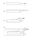
図1(a)〜図1(d)は、本発明の第1の実施形態に係る素子の1要素となるアモルファスシリコン薄膜の製造工程を示す断面図である。本実施形態においては、アモルファスシリコン薄膜の光劣化を、シアノイオン(CN- )を有する化合物(シアン化合物)にさらすことによって改善したアモルファスシリコン薄膜の形成方法について説明する。
【0045】
まず、図1(a)に示す工程で、ガラス基板1を準備し、このガラス基板1の主面を洗浄して、主面を清浄にしておく。
【0046】
次に、図1(b)に示す工程で、ガラス基板1をプラズマCVD用のチャンバー(図示せず)内に設置し、チャンバー内を排気して、10-8〜10-6Paまで減圧する。そして、チャンバー内にシラン(SiH4 )ガスを、チャンバー内の圧力が約13Paになるように流す。そして、プラズマ発生用電極に13.56MHzの高周波を印加して、プラズマを発生させる。その際、RFパワーは約0.04Wcm-2,基板温度は約250℃とする。約60分の反応により、図1(b)に示すように、ガラス基板1の上には、厚みが約500nmのi型(イントリンシック)アモルファスシリコン薄膜2が形成された。このグロー放電法によって形成されたアモルファスシリコン薄膜2中のシリコン原子の未結合手は水素によって終端されている。つまり、アモルファスシリコン薄膜2はいわゆる水素化アモルファスシリコンによって構成されている。
【0047】
次に、図1(c)に示す工程で、処理用基板をプラズマCVD処理用チャンバーから取り出して、基板を真空蒸着用チャンバー内に設置する。ただし、同じチャンバ内でCVDと真空蒸着とを行なってもよい。そして、真空蒸着用チャンバーの中で、真空蒸着法により、i型アモルファスシリコン薄膜2の上に、電気伝導度測定用の2本のT型アルミニウム電極3を形成する。その際、2本のT型アルミニウム電極3同士のギャップを0.1mmとしている。
【0048】
次に、図1(d)に示す工程で、処理用基板を真空蒸着用チャンバーから取り出して、処理槽6中の濃度0.01モル,25℃のシアン化カリウム(KCN)水溶液4中に浸漬する。その後、基板を100℃の超純水中に浸漬して、10分間の洗浄を行なう(以下、“シアン処理”と呼ぶ)。
【0049】
ここで、このシアン処理においては、シアン化カリウム(KCN)の代わりにシアン化ナトリウム(NaCN)などの他のシアン化合物を用いてもよい。また、このシアン処理を行なってから、図1(c)に示す工程を行なって、T型アルミニウム電極3を形成してもよい。
【0050】
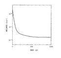
図2は、本実施形態のシアン処理を行なったアモルファスシリコン薄膜の光伝導度の変化を示す図である。同図において、横軸は光の照射時間(分)を表し、縦軸は光伝導度(Scm-2)(つまり光を照射しているときの電気伝導度)を表している。光照射は、擬似太陽光源AM1.5を用い、強度を100mWcm-2として行なっている。図2からわかるように、アモルファスシリコン薄膜を形成してからシアン処理を行なった場合、アモルファスシリコン薄膜に光を照射しても光伝導度はほとんど変化していない。
【0051】
一方、図3は、シアン処理を行なっていないアモルファスシリコン薄膜の光伝導度を示す図である。図3における横軸と縦軸とは、図2と同じパラメータを表している。図3からわかるように、シアン処理を行なっていないアモルファスシリコン薄膜に光を照射すると、時間の経過につれて光伝導度が減小していく。
【0052】
すなわち、図2及び図3のデータを併せると、アモルファスシリコン薄膜の光劣化がシアン処理によって確実に防止されていることがわかる。しかも、シアン処理を行なったアモルファスシリコン薄膜の光伝導度は、シアン処理を行なわなかったアモルファスシリコン薄膜の光照射前の光伝導度よりも大きい。すなわち、シアン処理により、アモルファスシリコン薄膜が形成された時点で存在している光伝導度の低下の原因となるもの(欠陥,再結合中心など)が消滅して、使用開始時からの光伝導度自体が向上しているものと考えられる。
【0053】
そして、この光伝導度の向上により、このアモルファスシリコン層を光電変換素子の要素として使用すれば、高い光電変換効率を発揮することが期待される。
【0054】
なお、本実施形態のアモルファスシリコン薄膜については、暗伝導度(光を照射しない状態での電電気伝導度)も測定している。図4は、本実施形態におけるシアン処理を行なったアモルファスシリコン薄膜の光照射時間に対する暗伝導度の変化を示す図であって、光を照射し、所定時間後に光を遮断して暗伝導度を測定した結果得られたデータを示している。同図に示すように、アモルファスシリコン薄膜にシアン処理を行なうことにより、光照射を行なっても暗伝導度は変化しないことがわかる。一方、図5は、シアン処理を行なっていないアモルファスシリコン薄膜の光照射時間に対する暗伝導度の変化を示す図である。同図に示すように、シアン処理を行なわなかった場合は、暗伝導度が光の照射時間の経過につれて、著しく低下していることがわかる。
【0055】
ここで、暗伝導度自体は、光電変換効率にはあまり関与しないファクターと考えられるが、暗伝導度の安定化は電子写真感光体や光センサの特性向上に有用である。図4及び図5に示されるデータからも、本実施形態のアモルファスシリコン薄膜により、従来問題となっていた光劣化を有効に防止し、素子の信頼性を高めうることが裏付けられている。
【0056】
−シアン処理によって光伝導度特性が改善される機構−
以上のようなシアン処理によってアモルファスシリコン薄膜の光劣化が防止され、かつ、光伝導度自体が向上する理由が現時点で発明者によって解明されているわけではないが、発明者がもっとも合理的と考えている機構について、以下、説明する。
(A)光照射前にシアン処理を行なう場合
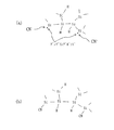
図12(a)及び図12(b)は、それぞれアモルファスシリコン薄膜の形成直後とシアン処理後とにおけるアモルファスシリコン薄膜の原子の結合状態を模式的に示す図である。
【0057】
図12(a)に示すように、水素化アモルファスシリコン薄膜を形成した直後においては、アモルファスシリコン薄膜中において、相隣接するSi原子間で結合されていない部分はほとんどH原子で終端されていると考えられる。しかし、このH原子によって終端されていてもその結合力が弱い部分があり得る。また、Si原子同士が結合している部分においても、その結合力が弱かったり、大きなひずみが存在していることがあり得る。結晶構造体に比べ、アモルファス構造体においては、各原子の並びが不規則であるためにそのような局部的に結合力の弱い結合部や、大きなひずみを有する結合部が多く存在しているものと考えられる。そして、アモルファスシリコンに光が照射されると、これらの不完全な結合部にダングリングボンドや欠陥準位が生成される。欠陥準位は、禁制帯内にエネルギー準位を有しているので、これが再結合中心として機能することにより、光伝導度が低下する,つまり光劣化が生じるものと考えられる。
【0058】
ところが、このアモルファスシリコン薄膜をシアン化合物の溶液中に浸漬することによって、図12(b)に示すように、アモルファスシリコン薄膜中の固有のダングリングボンドや、結合力の弱い結合部やひずみが存在する結合部などの不完全な結合にCN- イオンが作用して、Si−CN結合が形成されると考えられる。Si−CN結合は強固であるので、光照射によって切断されることはない。すなわち、不完全な結合部などが光照射に対して不活性化され、光照射に対して光劣化のない安定なアモルファスシリコン薄膜となる。また、光照射前にアモルファスシリコン薄膜中に存在していた欠陥準位も消失あるいは減少するために、光伝導度が向上すると考えられる。また、CN- イオンは小さなイオンであるので、アモルファスシリコン薄膜の表面から容易にアモルファスシリコン薄膜の内部に浸透することができ、その内部の不完全な結合に作用して、これを不活性化すると考えられる。
(B)光照射後にシアン処理を行なう場合
図13(a),図13(b)は、それぞれ光照射を受けた直後とその後シアン処理がされた後におけるアモルファスシリコン薄膜の原子の結合状態を模式的に示す図である。
【0059】
図13(a)に示すように、アモルファスシリコン薄膜に光照射を行なうと、上述のような結合力の弱い結合部、ひずみの存在する結合部などの不完全な結合部において、結合状態が破壊されてダングリングボンドなどの欠陥が生成する。このダングリングボンドなどの欠陥は、アモルファスシリコンの禁制帯中にエネルギー準位を有しているので、光伝導度の低下をもたらす。
【0060】
ところが、このアモルファスシリコン薄膜をシアン化合物の溶液に浸漬すると、図13(b)に示すように、ダングリングボンド等の欠陥にCN- イオンが作用して、Si−CN結合が形成されると考えられる。その結果、アモルファスシリコン薄膜の光伝導度が回復し、その後の光照射によっても光伝導度が低下することがないものと考えられる。
【0061】
(第2の実施形態)
次に、第2の実施形態においては、光照射が行なわれて光劣化が生じたアモルファスシリコン薄膜の光伝導度を回復させるための処理について説明する。
【0062】
本実施形態においても、アモルファスシリコン薄膜は、シアン処理工程を除いて、上記第1の実施形態と同じ工程によって形成されたものである。すなわち、図1(c)に示すように、ガラス基板1の上に形成されたアモルファスシリコン薄膜2であって、図1(d)に示すシアン処理は施されていない。
【0063】
図6は、本実施形態に係るアモルファスシリコン薄膜に光照射を行なったときの光照射時間の経過に対する光伝導度の変化を示す図である。ここでは、アモルファスシリコン薄膜の形成後、擬似太陽光線MA1.5を強度100mWcm-2で500時間の間照射した後、アモルファスシリコン薄膜にシアン処理を施し、その後、再び光照射を続けている。このシアン処理は、上記第1の実施形態と同様の条件の下で図1(d)に示すように行なっている。
【0064】
図6に示されるように、いったん光照射によって光劣化が生じたアモルファスシリコン薄膜に対しても、シアン処理を行なうことにより、光伝導度を回復させることができることがわかる。しかも、このデータでは、シアン処理が施されたアモルファスシリコン薄膜の光伝導度は、アモルファスシリコン薄膜に光を照射する前の光伝導度よりも高い値まで回復し、その後光照射を続けても低下していない。
【0065】
従って、本実施形態のシアン処理によって、光劣化が生じたアモルファスシリコン薄膜の光伝導度を回復させることができる。つまり、本実施形態のアモルファスシリコン薄膜を太陽電池に応用することにより、使用中に光劣化によって光電変換効率が低下した太陽電池の光電変換効率を回復させることができる。
【0066】
(第3の実施形態)
次に、上記第1の実施形態のアモルファスシリコン薄膜の応用である太陽電池に関する第3の実施形態について説明する。図7(a)〜図7(f)は、本実施形態におけるアモルファスシリコン太陽電池の製造工程を示す断面図である。
【0067】
まず、図7(a)に示す工程で、透明導体材料である酸化すず(SnO2 )により構成されるSnO2 基板11を準備して、SnO2 基板11を洗浄する。なお、SnO2 基板に代えて、ITO(Indium Tin Oxide)などの透明導体材料からなる基板を用いてもよい。
【0068】
次に、図7(b)に示す工程で、SnO2 基板11をプラズマCVD用3室分離真空槽(図示せず)内に取り付けて、真空槽内を排気して10-8〜10-6Paまで減圧する。さらに、プラズマCVD用3室分離真空槽の第1反応室において、水素と、水素によって10%に希釈されたシラン(SiH4 )ガスとを、第1反応室内の圧力が約13Paになるように流す。このシランガスには0.1〜数%(例えば約1.5%)のジボラン(B2 H6 )が含まれている。なお、ジボランに代えてトリメチルボロン(B(CH)3 )を用いることもできる。この雰囲気中で、基板温度を250℃とし、13.56MHzの高周波電力を約0.5Wcm-2のパワーで印加して、第1反応室内にプラズマを発生させる。この処理により、SnO2 基板11の上に、厚みが約20nmのp型シリコン微結晶層12が形成される。
【0069】
次に、図7(c)に示す工程で、処理用基板を、プラズマCVD用3室分離真空槽(図示せず)のうちの第1反応室から第2反応室に移動させて、第2反応室内に、シラン(SiH4 )を、第2反応室内の圧力が約13Paになるように流す。この雰囲気中で、基板温度を約250℃とし、13.56MHzの高周波電力を約0.04Wcm-2のパワーで印加して、第2反応室内にプラズマを発生させる。この処理により、p型シリコン微結晶層12の上に、厚みが約0.5μmのi型アモルファスシリコン層13が形成される。
【0070】
次に、図7(d)に示す工程で、処理用基板を、プラズマCVD用3室分離真空槽(図示せず)のうちの第2反応室から第3反応室に移動させて、第3反応室内に、水素と、水素によって10%に希釈されたシラン(SiH4 )とを、第3反応室内の圧力が約13Paになるように流す。このシランガスには0.1〜数%(例えば約1.5%)のフォスフィン(PH3 )が含まれている。この雰囲気中で、基板温度を320℃とし、13.56MHzの高周波電力を約0.5Wcm-3のパワーで印加して、第3反応室内にプラズマを発生させる。この処理により、i型アモルファスシリコン層13の上に、厚みが約20nmのn型シリコン微結晶層14が形成される。
【0071】
次に、図7(e)に示す工程で、処理用基板をプラズマCVD用3室分離真空槽から取り出して、処理槽18内で濃度0.01モル,温度25℃に調整されたシアン化カリウム水溶液15に、2分間浸漬する。その後、処理用基板を100℃の超純水によって洗浄する。
【0072】
次に、図7(f)に示す工程で、n型シリコン微結晶層14の上に、裏面電極となるアルミニウム電極16を形成する。
【0073】
なお、アルミニウム電極16を形成してから、図7(a)に示すシアン処理工程を行なってもよい。
【0074】
その後の工程は図示しないが、アルミニウム電極16とSnO2 基板11とからリード線を引き出すことにより、光劣化のほとんどないi型アモルファスシリコン層13を有する太陽電池として使用することができる。
【0075】
本実施形態の製造工程により形成されるアモルファスシリコン太陽電池においても、上記第1の実施形態と同様に、光劣化のないi型アモルファスシリコン層13が得られることが確認された。これは、n型シリコン微結晶層14によって覆われているアモルファスシリコン層13までCN- 基が侵入できることによるものと推定される。
【0076】
したがって、本実施形態のアモルファスシリコン太陽電池によると、光劣化のない、かつ、光伝導度の高いi型アモルファスシリコン層13を有しているので、光電変換効率の高い、かつ、光照射後にも光電変換効率の低下のないアモルファスシリコン太陽電池を得ることができる。
【0077】
(第4の実施形態)
次に、集積型アモルファスシリコン太陽電池に関する第4の実施形態について説明する。
【0078】
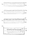
図8は、本実施形態における集積型アモルファスシリコン太陽電池の一部を示す断面図である。同図に示すように、ガラス基板20の上には、多数のセルが集積して設けられており、各セルは、酸化すず(SnO2 )等の透明導体材料(TCO:Transparent Conductive Oxide)からなる透明電極21aと、アモルファスシリコン層を含む半導体層22aと、半導体層22aの両側面上に形成された絶縁体サイドウォールSWと、アルミニウム等の金属からなる裏面電極23aとを備えている。
【0079】
図9は、図8に示す太陽電池の1つのセルの一部を拡大して示す断面図である。同図に示すように、半導体層22aは、さらに3つの層に分かれている。すなわち、下方から順に、p型不純物であるボロンがドープされたp型シリコン微結晶層25と、不純物がドープされていないi型アモルファスシリコン層26と、n型不純物であるリンがドープされたn型シリコン微結晶層27とが積層されており、これらの積層膜によって半導体層22aが構成されている。
【0080】
そして、1つのセルの裏面電極23aは、半導体層22aの最上部に設けられているn型シリコン微結晶層27に接続されているとともに、当該セルに隣接するセルの透明電極21aにも接続されている。つまり、各セル同士が直列に接続された構造となっている。
【0081】
ここで、透明電極21aには、SnO2 のほかITO(Indium Tin Oxide)などを用いてもよい。また、裏面電極23aには、アルミニウムのほかステンレス等の他の金属を用いてもよい。
【0082】
図10(a)〜図10(d)は、本実施形態におけるアモルファスシリコン太陽電池の製造工程のうちシアン処理を行なうまでの工程を示す断面図である。図11(a)〜図11(c)は、本実施形態におけるアモルファスシリコン太陽電池の製造工程のうちシアン処理の終了後裏面電極の形成までの工程を示す断面図である。
【0083】
まず、図10(a)に示す工程で、ガラス基板20の上に、真空蒸着法によりSnO2 膜21を形成し、さらに、図10(b)に示す工程で、SnO2 膜21をパターニングして、透明電極21aを形成する。このとき、SnO2 膜21をパターニングする方法としては、SnO2 膜21の上に、透明電極21aとして残す部分を覆うメタルマスク又はレジストマスクを作成してから、エッチングによりSnO2 膜21をパターニングする方法や、レーザーでSnO2 膜21を選択的に除去しながら透明電極21aのパターンに仕上げる方法などがあり、いずれを用いてもよい。
【0084】
次に、図10(c)に示す工程で、基板上に、図9に示す構造を有する積層膜22を堆積する。このときの手順は、第3の実施形態において説明したとおりである。すなわち、処理用基板をプラズマCVD用3室分離真空槽(図示せず)内に取り付けて、真空槽中の第1反応室内で厚みが約20nmのp型シリコン微結晶層25を、第2反応室内で厚みが約0.5μmのi型アモルファスシリコン層26を、第3反応室内で厚みが約20nmのn型シリコン微結晶層27を、それぞれ第3の実施形態において説明した条件下において形成する。
【0085】
次に、図10(d)に示す工程で、処理用基板をプラズマCVD用3室分離真空槽から取り出して、処理槽30内で濃度0.01モル,温度25℃に調整されたシアン化カリウム水溶液31に、2分間浸漬する。その後、処理用基板を100℃の超純水によって洗浄する。
【0086】
次に、図11(a)に示す工程で、積層膜22をパターニングして、各セルごとに分離され、透明電極21aの上面から一方の側面にまたがる半導体層22aを形成する。次に、基板の全面上にシリコン酸化膜を堆積し、異方性エッチングによりシリコン酸化膜をエッチバックして、各半導体層22aの両側面上に絶縁体サイドウォールSWを形成する。
【0087】
次に、図11(b)に示す工程で、基板の全面上にアルミニウム膜23を堆積した後、図11(c)に示す工程で、このアルミニウム膜23をパターニングして、裏面電極23aを形成する。このとき、1つのセルの裏面電極23aは、半導体層22a中のn型シリコン微結晶層27から一方の絶縁体サイドウォールSWを経て当該セルに隣接するセルの透明電極21aまで延びるようにパターニングされる。つまり、1つのセルの裏面電極23aは、半導体層22a中の最上部に位置するn型シリコン微結晶層27に接触するとともに、当該セルに隣接するセルの透明電極21aにも接触している。
【0088】
なお、図11(b)又は図11(c)に示す工程の後で、図10(d)に示すシアン処理を行なってもよい。
【0089】
以上の工程によって、図8に示す集積型アモルファスシリコン太陽電池が形成される。
【0090】
本実施形態の集積型アモルファスシリコン太陽電池及びその製造方法によると、所望の電圧値を得るための太陽電池の構造を容易に得ることができる。そして、この集積型アモルファスシリコン太陽電池においても、上記第3の実施形態と同様に、光電変換効率の向上と、光伝導度の低下に起因する光電変換効率の低下の防止とを図ることができる。
【0091】
(第5の実施形態)
次に、単結晶シリコン又はポリシリコンを用いた太陽電池に関する第5の実施形態について説明する。図14は、本実施形態における太陽電池の構造を示す斜視図である。
【0092】
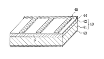
動ずに示すように、本実施形態の太陽電池は、単結晶シリコン又はポリシリコンからなりp型不純物(たとえばボロン)を含むpシリコン層41と、単結晶シリコン又はポリシリコンからなりn型不純物(たとえばリン)を含むn+ シリコン層42とを積層してなるpn接合シリコン層40を備えている。そして、pシリコン層41の下面には裏面電極43が設けられ、n+ シリコン層42の上面にはシリコンとは屈折率の異なる絶縁体材料(たとえばシリコン酸化膜)からなる反射防止膜44と、反射防止膜44の一部に設けられた開口部を介してn+ シリコン層42に接触するフィンガー電極45とが設けられている。
【0093】
ここで、本実施形態の太陽電池の製造工程においては、たとえば、以下の手順による処理を行なう。まず、単結晶シリコン薄板,ポリシリコンリボンなどに、不純物の拡散によりpn接合シリコン層40を形成した後に、上記第2,第3の実施形態と同様に、処理槽内でシアン化カリウム水溶液などのシアン化物溶液に浸漬する処理を行なう。このシアン処理の後、反射防止膜44の形成と、フィンガー電極45,裏面電極43の形成とを行なう。ただし、反射防止膜44の形成直後、又はフィンガー電極45の形成直後にシアン処理を行なってもよい。
【0094】
したがって、本実施形態の単結晶シリコン又はポリシリコン太陽電池によると、シアンか処理によってpシリコン層41及びn+ シリコン層42中のダングリングボンドを終端させることにより、光劣化のない、かつ、光伝導度の高いpシリコン層41及びn+ シリコン層42が得られるので、光電変換効率の高い、かつ、光照射後にも光電変換効率の低下のない太陽電池を得ることができる。
【0095】
特に、ポリシリコン太陽電池においては、ポリシリコンの粒界などに多く存在するダングリングボンドの存在によって太陽光の照射による光劣化が生じやすいが、本実施形態のシアン処理を行なうと、ダングリングボンドがCN- 基により終端されるので、光劣化が生じたポリシリコン薄膜の光伝導度を回復させることができる。
【0096】
(その他の実施形態)
上記第3,第4の実施形態においては、i型アモルファスシリコン層の上下にp型又はn型のシリコン微結晶層を設けたが、これらのシリコン微結晶層のうちの双方又はいずれか一方のシリコン微結晶層は必ずしも必要でない。金属−i型アモルファスシリコン層間のショットキー接合又はオーミック接合を介して、電荷を電極に取り出すようにしてもよいからである。
【0097】
また、第3,第4の実施形態におけるi型アモルファスシリコン層の上下双方に又は上下のうちいずれか一方の側に、シリコン微結晶層に代えて、p型アモルファスシリコン及びn型アモルファスシリコンなどからなる半導体層を設けてもよい。
【0098】
さらに、第3,第4の実施形態におけるi型アモルファスシリコン層に代えて、i型シリコン微結晶層を設けてもよい。
【0099】
また、上記第5の実施形態においては、pシリコン層41とn+ シリコン層42とが直接接触しているpn接合シリコン接合層40を設けたが、pシリコン層41とn+ シリコン層42との間にiシリコン層を介在させて、pin接合構造にしてもよい。
【0100】
上記各実施形態においては、シアン処理方法として、アモルファスシリコン層が形成されている処理用基板を、シアノイオンを含む液体中に浸漬する方法のみを開示しているが、そのほかにも、処理用基板の表面にKCN,NaCN等のシアノイオンを含む液体を流す方法や、処理用基板の表面にシアノイオンを含む液体を噴霧する方法などがあり、いずれを用いても上記各実施形態と同様の効果を発揮することができる。
【0101】
また、上記第2〜第5の実施形態においては、シリコン光電変換素子として太陽電池を構成した例について説明したが、本発明はかかる実施形態に限定されるものではなく、例えば複写機に用いられる感光ドラムやTFTなどの各種シリコン光電変換素子に用いることができる。
【0102】
特に、アモルファスシリコン層,ポリシリコン層又はシリコン微結晶層と導体層との間に介在する絶縁体層をさらに設けることで、TFTなど各種の光電変換素子を得ることができる。その場合、絶縁体層を構成する材料としては、二酸化シリコン(SiO2 ),一酸化シリコン(SiO),四窒化三シリコン(Si3 N4 ),シリコンオキシナイトライド,二酸化チタン(TiO2 ),三酸化アルミニウム(Al2 O3 )及び三酸化タングステン(WO3 )から選ばれた少なくともいずれか1つの物質により構成されていることが好ましい。
【0103】
上記第3,第4の実施形態において、基板をアルミニウム,ステンレスなどの不透明な金属により構成し、電極を透明導体材料(TCO)により構成してもよい。
【0104】
上記第3,第4及び第5の実施形態においては、ガラス基板に代えて、プラスチックフィルム,プラスチックフィルム上にステンレス膜やアルミニウム膜を形成したものを用いることもできる。
【0105】
【発明の効果】
本発明のシリコン光電変換素子,その製造方法又はその処理方法によると、シアン化処理によってシリコン層中の結合の欠陥部分にCN- 基を導入することで、光照射に対する光伝導度の低下の防止と、光伝導度の向上とにより、光電変換特性の高い太陽電池などの提供を図ることができる。
【図面の簡単な説明】
【図1】(a)〜(d)は、本発明の第1の実施形態に係る太陽電池の1要素となるアモルファスシリコン薄膜の製造工程を示す断面図である。
【図2】第1の実施形態のシアン処理を行なったアモルファスシリコン薄膜の光照射時間に対する光伝導度の変化を示す図である。
【図3】シアン処理を行なっていない従来のアモルファスシリコン薄膜の光照射時間に対する光伝導度の変化を示す図である。
【図4】第1の実施形態におけるシアン処理を行なったアモルファスシリコン薄膜の光照射時間に対する暗伝導度の変化を示す図である。
【図5】シアン処理を行なっていない従来のアモルファスシリコン薄膜の光照射時間に対する暗伝導度の変化を示す図である。
【図6】第2の実施形態に係るアモルファスシリコン薄膜に光照射を行なったときの光照射時間の経過に対する光伝導度の変化を示す図である。
【図7】(a)〜(f)は、第3の実施形態におけるアモルファスシリコン太陽電池の製造工程を示す断面図である。
【図8】第4の実施形態における集積型アモルファスシリコン太陽電池の一部を示す断面図である。
【図9】図8に示す太陽電池の1つのセルの一部を拡大して示す断面図である。
【図10】(a)〜(d)は、第4の実施形態におけるアモルファスシリコン太陽電池の製造工程のうちシアン処理を行なうまでの工程を示す断面図である。
【図11】(a)〜(c)は、第4の実施形態におけるアモルファスシリコン太陽電池の製造工程のうちアイアン処理の終了後裏面電極の形成までの工程を示す断面図である。
【図12】(a),(b)は、それぞれアモルファスシリコン薄膜の形成直後とシアン処理後とにおけるアモルファスシリコン薄膜の原子の結合状態を模式的に示す図である。
【図13】(a),(b)は、それぞれ光照射を受けた直後とその後シアン処理がされた後におけるアモルファスシリコン薄膜の原子の結合状態を模式的に示す図である。
【図14】第5の実施形態におけるシリコン太陽電池の構造を示す断面図である。
【符号の説明】
1 ガラス基板
2 i型アモルファスシリコン層
3 T型アルミニウム電極
4 シアン化カリウム水溶液
6 処理槽
11 SnO2 基板
12 p型シリコン微結晶層
13 i型アモルファスシリコン層
14 n型シリコン微結晶層
15 シアン化カリウム水溶液
16 アルミニウム電極
18 処理槽
20 ガラス基板
21 SnO2 膜
21a 透明電極
22 積層膜
22a 半導体層
25 p型シリコン微結晶層
26 i型アモルファスシリコン層
27 n型シリコン微結晶層
30 処理槽
31 シアン化カリウム水溶液
41 pシリコン層
42 n+ シリコン層
43 裏面電極
44 反射防止膜
45 フィンガー電極[0001]
BACKGROUND OF THE INVENTION
The present invention relates to a method for processing a semiconductor device made of silicon and a method for manufacturing the same, and more particularly, to measures for eliminating the photodegradation.
[0002]
[Prior art]
For example, as disclosed in the literature (DLStaebler, CRWronski: Applied Physics Letters, 31, No. 4, p. 292, 1977), the electrical conductivity of silicon during light irradiation (hereinafter referred to as “photoconductivity”) It is known that the electrical conductivity in the dark state (hereinafter referred to as “dark conductivity”) rapidly decreases as the light irradiation time elapses. This phenomenon is called “photodegradation (S-W effect)”, and the photoelectric conversion efficiency of the solar cell is reduced due to a decrease in the electrical conductivity (especially photoconductivity) of amorphous silicon. is important.
[0003]
Therefore, conventionally, for example, the following method has been adopted in order to suppress a change in photoconductivity of amorphous silicon due to light irradiation.
[0004]
As a first method, when an amorphous silicon film is formed by CVD, silane gas (SH Four ) Instead of SiD Four (For example, Koji Dairiki, Seiichi Suzuki, Akira Yamada, Makoto Konagai: Technical Digest of the International PVSEC-9.pp.373, 1996).
[0005]
As a second method, in the CVD method, instead of silane gas, SiF Four (For example, Y. Kuwano, M. Ohnisi, H. Nishiwaki, S. Tsuda, H. Shibuya, S. Nakano: Proceeding of 15th IEEE Photovoltaic Specialists Conference, p. 698).
[0006]
As a third method, there is a method of suppressing light degradation by forming a pinpin structure with a double pin structure and reducing the film thickness of the i layer between the p layer and the n layer.
[0007]
[Problems to be solved by the invention]
However, the conventional methods have the following problems.
[0008]
In the first method, SiD Four In addition to being expensive, the change in photoconductivity due to light irradiation can be suppressed to some extent, but the change in photoconductivity cannot be completely eliminated.
[0009]
In the second method, SiF Four In addition to increasing the discharge power for producing amorphous silicon to about 10 times that when silane gas is used, impurities are easily incorporated into the formed film, and the film quality deteriorates. There is a problem that it is easy to do.
[0010]
In the third method, there is a problem that the manufacturing cost for creating the pinpin structure is high, and furthermore, light degradation cannot be reliably prevented.
[0011]
Moreover, the phenomenon of light degradation as described above also exists in polysilicon, microcrystalline silicon, single crystal silicon, and the like. For example, it is known that a large number of silicon dangling bonds exist in the grain boundary particularly in microcrystalline silicon and polysilicon. Further, even in single crystal silicon, dangling bonds exist when recovery after an amorphous structure is obtained by ion implantation or the like is insufficient. Accordingly, when amorphous silicon, polysilicon, microcrystalline silicon, single crystal silicon, or the like is used as a material constituting a photoelectric conversion element such as a solar cell or an optical sensor, there is a risk of deteriorating optical characteristics such as a photoelectric conversion rate. there were.
[0012]
The object of the present invention is to provide high conversion efficiency at a practical cost by providing means for easily preventing the occurrence of defects such as amorphous silicon, polysilicon, single crystal silicon, and microcrystalline silicon that cause photodegradation. It is providing the processing method for obtaining a silicon photoelectric conversion element, and its manufacturing method.
[0013]
[Means for Solving the Problems]
The silicon photoelectric conversion element of the present invention includes a silicon layer containing a CN group and a conductor layer provided on either the upper or lower side of the silicon layer.
[0014]
As a result, a defect portion such as a dangling bond in the silicon layer, a weakly bonded portion, or a strained portion is replaced with a CN group, that is, a recombination center of carriers excited by light irradiation. A structure with almost no defects is obtained. Therefore, a device having a high characteristic such as a solar cell, a photosensor, and a photoconductor (electrophotographic) having a high characteristic such as photoconductivity and having almost no deterioration over time such as a decrease in photoconductivity due to light irradiation. ) Etc. will be obtained.
[0015]
The silicon layer is preferably composed of any one material selected from amorphous silicon, polysilicon, microcrystalline silicon, and single crystal silicon.
[0016]
In the silicon photoelectric conversion element, the conductor layer is a lower conductor electrode of a solar cell, and further includes an upper conductor electrode provided on the silicon layer, whereby photoelectric conversion without deterioration due to irradiation of sunlight is performed. A highly efficient solar cell can be obtained.
[0017]
In the silicon photoelectric conversion device, by further including a lower semiconductor layer interposed between the lower conductor electrode and the silicon layer, it becomes possible to expand the width of the absorption spectrum of the device, The photoelectric conversion efficiency can be improved.
[0018]
In that case, the lower semiconductor layer is at least one selected from p-type or n-type microcrystalline silicon, p-type or n-type amorphous silicon, p-type or n-type polysilicon, and p-type or n-type single crystal silicon. It can be composed of one substance.
[0019]
The silicon photoelectric conversion element preferably further includes an upper semiconductor layer interposed between the upper conductor electrode and the silicon layer.
[0020]
Also in this case, the upper semiconductor layer is at least one selected from p-type or n-type microcrystalline silicon, p-type or n-type amorphous silicon, p-type or n-type polysilicon, and p-type or n-type single crystal silicon. Or a single substance.
[0021]
In the silicon photoelectric conversion element, one of the lower conductor electrode and the upper conductor electrode is constituted by a conductor transparent to sunlight, and the other is constituted by a conductor opaque to sunlight. Thereby, the absorption efficiency of sunlight can be improved.
[0022]
In the silicon photoelectric conversion element, by further including an insulator layer interposed between the silicon layer and the conductor layer, various elements such as TFTs can be configured.
[0023]
In the silicon photoelectric conversion element, the insulator layer includes silicon dioxide (SiO 2). 2 ), Silicon monoxide (SiO), trisilicon tetranitride (Si) Three N Four ), Silicon oxynitride, titanium dioxide (TiO) 2 ), Aluminum trioxide (Al 2 O Three ) And tungsten trioxide (WO Three It is preferable that it is composed of at least one substance selected from
[0024]
The method for producing a silicon photoelectric conversion element of the present invention includes a step (a) of forming a silicon layer on a substrate composed of a conductor material, a semiconductor material, or an insulator material, and a cyano ion CN on the silicon layer. - And (b) performing a cyan treatment for introducing.
[0025]
By this method, a cyano ion CN is formed in the silicon layer. - Permeates, cyano ions are bonded to defective portions such as dangling bonds in the silicon layer, and weakly bonded portions or strained portions are replaced with CN groups. Therefore, even when carriers are excited by light irradiation or the like, defects that become recombination centers of carriers are almost eliminated. As a result, an element having a high characteristic including a silicon layer having high characteristics such as photoconductivity and little deterioration with time of characteristics such as a decrease in photoconductivity with respect to light irradiation is formed.
[0026]
In the method for manufacturing a silicon photoelectric conversion element, in the step (a), the silicon layer is at least one layer selected from an amorphous silicon layer, a polysilicon layer, a microcrystalline silicon layer, and a single crystal silicon layer. Is preferably formed.
[0027]
In the method for producing a silicon photoelectric conversion element, in the step (b), the entire substrate is made of cyano ion CN. - It is the simplest method to immerse in a liquid containing
[0028]
In the method for manufacturing a silicon photoelectric conversion element, the substrate is made of an insulator material, and further includes a step of forming a lower conductor electrode on the substrate before performing the step (a), In the step (a), the silicon layer can be formed on the lower conductor electrode.
[0029]
The method for manufacturing the silicon photoelectric conversion device may further include a step of forming an upper conductor electrode on the silicon layer after performing the step (b) or before performing the step (b).
[0030]
The method for manufacturing a silicon photoelectric conversion device further includes a step of forming a lower semiconductor layer on the substrate before performing the step (a). In the step (a), the lower semiconductor layer is formed. The silicon layer can be formed on the substrate.
[0031]
The method for manufacturing a silicon photoelectric conversion device further includes a step of forming a lower conductor electrode on the substrate before performing the step (a). In the step (a), the lower conductor electrode is formed. The lower semiconductor layer can be formed on the substrate.
[0032]
The method for manufacturing the silicon photoelectric conversion device may further include a step of forming an upper conductor electrode on the silicon layer after the step (b) or before the step (b).
[0033]
The method for manufacturing a silicon photoelectric conversion element further includes a step of forming an upper semiconductor layer on the silicon layer after performing the step (a) and before performing the step (b). In the step (b), cyan treatment can be performed from above the upper semiconductor layer.
[0034]
Also in this case, the steps for forming the lower conductor electrode and the lower semiconductor layer as described above can be added.
[0035]
In the method for producing a silicon photoelectric conversion element, various elements such as TFTs can be formed by further including a step of forming an insulator layer on the silicon layer after performing the step (a). .
[0036]
Furthermore, after performing the said process (b), the process of forming a conductor electrode on the said insulator layer can also be further provided.
[0037]
Moreover, in the manufacturing method of the said silicon photoelectric conversion element, after performing the said process (a), before performing the said process (b), you may further provide the process of irradiating the said silicon layer.
[0038]
The method for processing a silicon photoelectric conversion element of the present invention comprises a step (a) of preparing a processing substrate having a silicon layer, and a cyano ion CN. - A step (b) of preparing a treatment liquid containing cyano ions CN in the silicon layer of the treatment substrate using the treatment liquid. - And (c) performing cyan processing for introducing.
[0039]
By this method, as described above, CN in the silicon layer in the processing substrate - Various characteristics such as photoelectric conversion characteristics of silicon can be improved by applying ions.
[0040]
In the silicon photoelectric conversion element processing method, in step (a), the silicon layer is at least one layer selected from an amorphous silicon layer, a polysilicon layer, a microcrystalline silicon layer, and a single crystal silicon layer. It is preferable to prepare a processing substrate having
[0041]
In the silicon photoelectric conversion element processing method, in the step (c), a method of immersing the processing substrate in the processing liquid is simple.
[0042]
In the silicon photoelectric conversion element processing method, the processing substrate further includes an upper semiconductor layer provided on the silicon layer, and in the step (c), cyan treatment is performed on the upper semiconductor layer. Can be done.
[0043]
In the silicon photoelectric conversion element processing method, even when light is irradiated on the silicon layer of the processing substrate before performing the step (c), the silicon layer whose photoconductivity is deteriorated by light irradiation. It becomes possible to restore the photoconductivity.
[0044]
DETAILED DESCRIPTION OF THE INVENTION
(First embodiment)
FIG. 1A to FIG. 1D are cross-sectional views showing a manufacturing process of an amorphous silicon thin film that is one element of an element according to the first embodiment of the present invention. In this embodiment, photodegradation of an amorphous silicon thin film is treated with cyano ions (CN - A method for forming an amorphous silicon thin film which has been improved by exposure to a compound (cyanide compound) having) will be described.
[0045]
First, in the step shown in FIG. 1A, a
[0046]
Next, in the step shown in FIG. 1B, the
[0047]
Next, in the step shown in FIG. 1C, the processing substrate is taken out from the plasma CVD processing chamber, and the substrate is placed in the vacuum deposition chamber. However, CVD and vacuum deposition may be performed in the same chamber. Then, two T-
[0048]
Next, in the step shown in FIG. 1 (d), the processing substrate is taken out from the vacuum deposition chamber and immersed in a potassium cyanide (KCN)
[0049]
Here, in this cyan treatment, other cyan compounds such as sodium cyanide (NaCN) may be used instead of potassium cyanide (KCN). Further, after performing the cyan treatment, the step shown in FIG. 1C may be performed to form the T-
[0050]
FIG. 2 is a graph showing changes in the photoconductivity of the amorphous silicon thin film subjected to the cyan treatment of this embodiment. In the figure, the horizontal axis represents light irradiation time (minutes), and the vertical axis represents photoconductivity (Scm). -2 ) (That is, electrical conductivity when light is irradiated). Light irradiation uses a pseudo solar light source AM1.5 and has an intensity of 100 mWcm. -2 It is done as. As can be seen from FIG. 2, when the cyan treatment is performed after the amorphous silicon thin film is formed, the photoconductivity hardly changes even when the amorphous silicon thin film is irradiated with light.
[0051]
On the other hand, FIG. 3 is a diagram showing the photoconductivity of an amorphous silicon thin film not subjected to cyan treatment. The horizontal and vertical axes in FIG. 3 represent the same parameters as in FIG. As can be seen from FIG. 3, when light is applied to an amorphous silicon thin film that has not been subjected to cyan treatment, the photoconductivity decreases with the passage of time.
[0052]
That is, when the data of FIG. 2 and FIG. 3 are combined, it can be seen that photodegradation of the amorphous silicon thin film is reliably prevented by the cyan treatment. Moreover, the photoconductivity of the amorphous silicon thin film subjected to the cyan treatment is larger than the photoconductivity of the amorphous silicon thin film not subjected to the cyan treatment before light irradiation. In other words, the cyanide treatment eliminates the photoconductivity (defects, recombination centers, etc.) that existed when the amorphous silicon thin film was formed, and the photoconductivity from the start of use. It is thought that it has improved.
[0053]
And by this improvement in photoconductivity, if this amorphous silicon layer is used as an element of a photoelectric conversion element, it is expected to exhibit high photoelectric conversion efficiency.
[0054]
In addition, about the amorphous silicon thin film of this embodiment, dark conductivity (electrical conductivity in the state which does not irradiate light) is also measured. FIG. 4 is a diagram showing a change in dark conductivity with respect to the light irradiation time of the amorphous silicon thin film subjected to the cyan treatment in the present embodiment. Light irradiation is performed, and light is blocked after a predetermined time to obtain dark conductivity. The data obtained as a result of the measurement are shown. As shown in the figure, it is understood that the dark conductivity does not change even when light irradiation is performed by performing cyan treatment on the amorphous silicon thin film. On the other hand, FIG. 5 is a diagram showing a change in dark conductivity with respect to light irradiation time of an amorphous silicon thin film not subjected to cyan treatment. As shown in the figure, it can be seen that when the cyan treatment is not performed, the dark conductivity is remarkably lowered as the light irradiation time elapses.
[0055]
Here, although the dark conductivity itself is considered to be a factor that is not so much involved in the photoelectric conversion efficiency, stabilization of the dark conductivity is useful for improving the characteristics of the electrophotographic photosensitive member and the optical sensor. The data shown in FIGS. 4 and 5 also support that the amorphous silicon thin film of this embodiment can effectively prevent light degradation that has been a problem in the past and can improve the reliability of the element.
[0056]
-Mechanism of improving photoconductivity characteristics by cyanide treatment-
The reason why the above-described cyan treatment prevents photodegradation of the amorphous silicon thin film and improves the photoconductivity itself is not yet elucidated by the inventor, but the inventor believes that it is the most reasonable. Hereinafter, the mechanism will be described.
(A) When cyan treatment is performed before light irradiation
FIG. 12A and FIG. 12B are diagrams schematically showing the bonding state of atoms in the amorphous silicon thin film immediately after the formation of the amorphous silicon thin film and after the cyan treatment, respectively.
[0057]
As shown in FIG. 12 (a), immediately after the hydrogenated amorphous silicon thin film is formed, the portion of the amorphous silicon thin film that is not bonded between adjacent Si atoms is almost terminated with H atoms. Conceivable. However, even if terminated by this H atom, there may be a portion where the binding force is weak. Further, even in a portion where Si atoms are bonded to each other, the bonding force may be weak or a large strain may exist. Compared to a crystal structure, an amorphous structure has many bonds with weak local bonds and bonds with large strains due to the irregular arrangement of atoms. it is conceivable that. When the amorphous silicon is irradiated with light, dangling bonds and defect levels are generated in these incomplete joints. Since the defect level has an energy level in the forbidden band, it functions as a recombination center, so that the photoconductivity decreases, that is, photodegradation occurs.
[0058]
However, by dipping this amorphous silicon thin film in a cyanide solution, there are inherent dangling bonds, weak bond strengths and strains in the amorphous silicon thin film, as shown in FIG. CN for incomplete connection such as connecting part - It is considered that ions act to form Si—CN bonds. Since the Si—CN bond is strong, it is not broken by light irradiation. That is, an incomplete bonding portion or the like is inactivated with respect to light irradiation, and a stable amorphous silicon thin film having no light deterioration with respect to light irradiation is obtained. In addition, it is considered that the defect level existing in the amorphous silicon thin film before the light irradiation disappears or decreases, so that the photoconductivity is improved. CN - Since the ions are small ions, they can easily penetrate into the amorphous silicon thin film from the surface of the amorphous silicon thin film, and act on incomplete bonding inside the thin film to inactivate it.
(B) When cyan treatment is performed after light irradiation
FIGS. 13A and 13B are diagrams schematically showing the bonding state of atoms in the amorphous silicon thin film immediately after receiving light irradiation and after being subjected to cyan treatment.
[0059]
As shown in FIG. 13 (a), when the amorphous silicon thin film is irradiated with light, the bonding state is broken in incomplete bonding portions such as the bonding portion having a weak bonding force and the bonding portion having strain as described above. As a result, defects such as dangling bonds are generated. Defects such as dangling bonds have an energy level in the forbidden band of amorphous silicon, resulting in a decrease in photoconductivity.
[0060]
However, when this amorphous silicon thin film is immersed in a cyanide compound solution, as shown in FIG. - It is considered that ions act to form Si—CN bonds. As a result, it is considered that the photoconductivity of the amorphous silicon thin film is recovered and the photoconductivity is not lowered by the subsequent light irradiation.
[0061]
(Second Embodiment)
Next, in the second embodiment, a process for recovering the photoconductivity of an amorphous silicon thin film that has been subjected to light irradiation and caused photodegradation will be described.
[0062]
Also in this embodiment, the amorphous silicon thin film is formed by the same process as that of the first embodiment except for the cyan treatment process. That is, as shown in FIG. 1C, the amorphous silicon
[0063]
FIG. 6 is a diagram showing the change in photoconductivity with the passage of light irradiation time when the amorphous silicon thin film according to this embodiment is irradiated with light. Here, after the formation of the amorphous silicon thin film, pseudo-sun rays MA1.5 are applied with an intensity of 100 mWcm. -2 After irradiation for 500 hours, the amorphous silicon thin film was subjected to cyan treatment, and then light irradiation was continued again. This cyan processing is performed as shown in FIG. 1D under the same conditions as in the first embodiment.
[0064]
As shown in FIG. 6, it can be seen that the photoconductivity can be recovered by performing cyan treatment even on an amorphous silicon thin film once subjected to light degradation by light irradiation. In addition, in this data, the photoconductivity of the amorphous silicon thin film treated with cyan is recovered to a value higher than the photoconductivity before the amorphous silicon thin film is irradiated with light, and then decreases even if light irradiation is continued. Not done.
[0065]
Therefore, the cyan conductivity of this embodiment can recover the photoconductivity of the amorphous silicon thin film in which the photodegradation has occurred. That is, by applying the amorphous silicon thin film of this embodiment to a solar cell, it is possible to recover the photoelectric conversion efficiency of the solar cell in which the photoelectric conversion efficiency is reduced due to light degradation during use.
[0066]
(Third embodiment)
Next, a third embodiment relating to a solar cell, which is an application of the amorphous silicon thin film of the first embodiment, will be described. FIG. 7A to FIG. 7F are cross-sectional views showing a manufacturing process of the amorphous silicon solar cell in the present embodiment.
[0067]
First, in the step shown in FIG. 7A, tin oxide (SnO), which is a transparent conductor material, is used. 2 SnO 2 Prepare
[0068]
Next, in the step shown in FIG. 2 The
[0069]
Next, in the step shown in FIG. 7C, the processing substrate is moved from the first reaction chamber to the second reaction chamber in a three-chamber separation vacuum chamber (not shown) for plasma CVD, and second In the reaction chamber, silane (SiH Four ) So that the pressure in the second reaction chamber is about 13 Pa. In this atmosphere, the substrate temperature is about 250 ° C., and the high frequency power of 13.56 MHz is about 0.04 Wcm. -2 To generate plasma in the second reaction chamber. By this treatment, an i-type
[0070]
Next, in the step shown in FIG. 7D, the processing substrate is moved from the second reaction chamber to the third reaction chamber in the three-chamber separation vacuum chamber (not shown) for plasma CVD, and the third In the reaction chamber, hydrogen and silane (SiH diluted to 10% with hydrogen) Four ) So that the pressure in the third reaction chamber is about 13 Pa. This silane gas contains 0.1 to several percent (for example, about 1.5%) of phosphine (PH Three )It is included. In this atmosphere, the substrate temperature is set to 320 ° C., and high frequency power of 13.56 MHz is about 0.5 Wcm. -3 To generate plasma in the third reaction chamber. By this treatment, an n-type
[0071]
Next, in the step shown in FIG. 7E, the processing substrate is taken out of the three-chamber separation vacuum tank for plasma CVD, and the potassium cyanide aqueous solution 15 adjusted to a concentration of 0.01 mol and a temperature of 25 ° C. in the
[0072]
Next, in the step shown in FIG. 7F, an aluminum electrode 16 serving as a back electrode is formed on the n-type
[0073]
In addition, after forming the aluminum electrode 16, you may perform the cyan treatment process shown to Fig.7 (a).
[0074]
Although the subsequent steps are not shown, the aluminum electrode 16 and SnO 2 By pulling out the lead wire from the
[0075]
Also in the amorphous silicon solar cell formed by the manufacturing process of this embodiment, it was confirmed that the i-type
[0076]
Therefore, according to the amorphous silicon solar cell of this embodiment, since it has the i-type
[0077]
(Fourth embodiment)
Next, a fourth embodiment relating to an integrated amorphous silicon solar cell will be described.
[0078]
FIG. 8 is a cross-sectional view showing a part of the integrated amorphous silicon solar cell in the present embodiment. As shown in the figure, a large number of cells are integrated and provided on the
[0079]
FIG. 9 is an enlarged cross-sectional view showing a part of one cell of the solar battery shown in FIG. As shown in the figure, the
[0080]
The
[0081]
Here, the
[0082]
FIG. 10A to FIG. 10D are cross-sectional views showing steps until the cyan treatment is performed in the manufacturing steps of the amorphous silicon solar cell in the present embodiment. FIG. 11A to FIG. 11C are cross-sectional views showing the steps from the end of cyan treatment to the formation of the back electrode in the manufacturing process of the amorphous silicon solar cell in the present embodiment.
[0083]
First, in the step shown in FIG. 10A, SnO is deposited on the
[0084]
Next, in the step shown in FIG. 10C, a
[0085]
Next, in the step shown in FIG. 10 (d), the processing substrate is taken out of the three chamber separation vacuum tank for plasma CVD, and the potassium cyanide aqueous solution 31 adjusted to a concentration of 0.01 mol and a temperature of 25 ° C. in the
[0086]
Next, in the step shown in FIG. 11A, the
[0087]
Next, after depositing an
[0088]
Note that cyan processing shown in FIG. 10D may be performed after the step shown in FIG. 11B or FIG. 11C.
[0089]
Through the above steps, the integrated amorphous silicon solar cell shown in FIG. 8 is formed.
[0090]
According to the integrated amorphous silicon solar cell and the manufacturing method thereof of the present embodiment, the structure of the solar cell for obtaining a desired voltage value can be easily obtained. Also in this integrated amorphous silicon solar cell, as in the third embodiment, it is possible to improve the photoelectric conversion efficiency and prevent the decrease in the photoelectric conversion efficiency due to the decrease in photoconductivity. .
[0091]
(Fifth embodiment)
Next, a fifth embodiment relating to a solar cell using single crystal silicon or polysilicon will be described. FIG. 14 is a perspective view showing the structure of the solar cell in the present embodiment.
[0092]
As will be shown, the solar cell of this embodiment includes a p-
[0093]
Here, in the manufacturing process of the solar cell of the present embodiment, for example, processing according to the following procedure is performed. First, after forming a pn
[0094]
Therefore, according to the single crystal silicon or polysilicon solar cell of this embodiment, the
[0095]
In particular, in a polysilicon solar cell, the presence of a dangling bond that is often present at the grain boundary of the polysilicon is likely to cause light degradation due to the irradiation of sunlight. Is CN - Since it is terminated by the base, it is possible to recover the photoconductivity of the polysilicon thin film in which the photodegradation has occurred.
[0096]
(Other embodiments)
In the third and fourth embodiments, the p-type or n-type silicon microcrystal layer is provided above and below the i-type amorphous silicon layer. However, both or any one of these silicon microcrystal layers is provided. The silicon microcrystalline layer is not always necessary. This is because the charge may be taken out to the electrode through a Schottky junction or an ohmic junction between the metal-i type amorphous silicon layers.
[0097]
Further, instead of the silicon microcrystalline layer, the p-type amorphous silicon, the n-type amorphous silicon, or the like is formed on both the upper and lower sides of the i-type amorphous silicon layer or on either one of the upper and lower sides in the third and fourth embodiments. A semiconductor layer may be provided.
[0098]
Further, an i-type silicon microcrystal layer may be provided in place of the i-type amorphous silicon layer in the third and fourth embodiments.
[0099]
In the fifth embodiment, the
[0100]
In each of the above-described embodiments, only a method of immersing a processing substrate on which an amorphous silicon layer is formed in a liquid containing cyano ions is disclosed as a cyan processing method. There are a method of flowing a liquid containing cyano ions such as KCN and NaCN on the surface of the substrate, and a method of spraying a liquid containing cyano ions on the surface of the processing substrate. Can be demonstrated.
[0101]
Moreover, in the said 2nd-5th embodiment, although the example which comprised the solar cell as a silicon photoelectric conversion element was demonstrated, this invention is not limited to this embodiment, For example, it is used for a copying machine. It can be used for various silicon photoelectric conversion elements such as a photosensitive drum and a TFT.
[0102]
In particular, by further providing an insulating layer interposed between the amorphous silicon layer, the polysilicon layer, or the silicon microcrystal layer and the conductor layer, various photoelectric conversion elements such as TFTs can be obtained. In that case, the material constituting the insulator layer is silicon dioxide (SiO 2). 2 ), Silicon monoxide (SiO), trisilicon tetranitride (Si) Three N Four ), Silicon oxynitride, titanium dioxide (TiO) 2 ), Aluminum trioxide (Al 2 O Three ) And tungsten trioxide (WO Three It is preferable that it is composed of at least one substance selected from
[0103]
In the third and fourth embodiments, the substrate may be made of an opaque metal such as aluminum or stainless steel, and the electrode may be made of a transparent conductor material (TCO).
[0104]
In the said 3rd, 4th and 5th embodiment, it can replace with a glass substrate and what formed the stainless steel film | membrane and the aluminum film on the plastic film and a plastic film can also be used.
[0105]
【The invention's effect】
According to the silicon photoelectric conversion element of the present invention, the manufacturing method thereof, or the processing method thereof, CN is formed on the defect portion of the bond in the silicon layer by the cyanation treatment. - By introducing a group, it is possible to provide a solar cell or the like having high photoelectric conversion characteristics by preventing reduction in photoconductivity with respect to light irradiation and improving photoconductivity.
[Brief description of the drawings]
FIGS. 1A to 1D are cross-sectional views showing a manufacturing process of an amorphous silicon thin film that is one element of a solar cell according to a first embodiment of the present invention.
FIG. 2 is a diagram showing a change in photoconductivity with respect to light irradiation time of an amorphous silicon thin film subjected to cyan treatment according to the first embodiment.
FIG. 3 is a diagram showing a change in photoconductivity with respect to light irradiation time of a conventional amorphous silicon thin film not subjected to cyan treatment.
FIG. 4 is a diagram showing a change in dark conductivity with respect to light irradiation time of an amorphous silicon thin film subjected to cyan treatment in the first embodiment.
FIG. 5 is a diagram showing a change in dark conductivity with respect to light irradiation time of a conventional amorphous silicon thin film not subjected to cyan treatment.
FIG. 6 is a diagram showing a change in photoconductivity with the passage of light irradiation time when light irradiation is performed on an amorphous silicon thin film according to the second embodiment.
FIGS. 7A to 7F are cross-sectional views showing the steps for manufacturing an amorphous silicon solar cell in the third embodiment. FIGS.
FIG. 8 is a cross-sectional view showing a part of an integrated amorphous silicon solar cell in a fourth embodiment.
9 is an enlarged cross-sectional view showing a part of one cell of the solar battery shown in FIG.
FIGS. 10A to 10D are cross-sectional views showing steps up to the cyan treatment in the manufacturing steps of the amorphous silicon solar cell in the fourth embodiment.
FIGS. 11A to 11C are cross-sectional views showing steps from the end of the iron process to the formation of the back electrode in the amorphous silicon solar cell manufacturing process according to the fourth embodiment. FIGS.
FIGS. 12A and 12B are diagrams schematically showing the bonding state of atoms in an amorphous silicon thin film immediately after the formation of the amorphous silicon thin film and after the cyan treatment, respectively.
FIGS. 13A and 13B are diagrams schematically showing the bonding state of atoms in an amorphous silicon thin film immediately after receiving light irradiation and after being subjected to cyan treatment, respectively.
FIG. 14 is a cross-sectional view showing the structure of a silicon solar cell in a fifth embodiment.
[Explanation of symbols]
1 Glass substrate
2 i-type amorphous silicon layer
3 T-type aluminum electrode
4 Potassium cyanide aqueous solution
6 treatment tank
11 SnO 2 substrate
12 p-type silicon microcrystal layer
13 i-type amorphous silicon layer
14 n-type silicon microcrystal layer
15 Potassium cyanide aqueous solution
16 Aluminum electrode
18 Treatment tank
20 Glass substrate
21 SnO 2 film
21a Transparent electrode
22 Multilayer film
22a Semiconductor layer
25 p-type silicon microcrystal layer
26 i-type amorphous silicon layer
27 n-type silicon microcrystal layer
30 treatment tank
31 Potassium cyanide aqueous solution
41 p silicon layer
42 n + Silicon layer
43 Back electrode
44 Anti-reflective coating
45 finger electrode
Claims (10)
前記i型シリコン層の上側に接して形成された第1導電型の上側半導体層と、
前記i型シリコン層の下側に接して形成された第2導電型の下側半導体層と、
前記上側半導体層の上に形成された上側導体電極と、
前記下側半導体層の下に形成された下側導体電極とを備え、
前記CN基は、前記i型シリコン層の内部に存在していることを特徴とする太陽電池。An i-type silicon layer containing a CN group;
An upper semiconductor layer of the first conductivity type formed in contact with the upper side of the front SL i-type silicon layer,
A second conductive type lower semiconductor layer formed in contact with the lower side of the i-type silicon layer;
An upper conductor electrode formed on the upper semiconductor layer;
A lower conductor electrode formed under the lower semiconductor layer ,
The said CN group exists in the said i-type silicon layer, The solar cell characterized by the above-mentioned.
前記上側半導体層及び前記下側半導体層のうちの一方はn型であり、他方はp型であることを特徴とする請求項1又は2に記載の太陽電池。The upper semiconductor layer and the lower semiconductor layer are made of at least one of microcrystalline silicon, amorphous silicon, polysilicon, and single crystal silicon ,
3. The solar cell according to claim 1, wherein one of the upper semiconductor layer and the lower semiconductor layer is n-type and the other is p-type .
前記下側導体電極及び上側導体電極の他方は、太陽光に対して不透明な導体からなることを特徴とする請求項1に記載の太陽電池。One of the lower conductor electrode and the upper conductor electrode is made of a conductor transparent to sunlight,
2. The solar cell according to claim 1 , wherein the other of the lower conductor electrode and the upper conductor electrode is made of a conductor that is opaque to sunlight.
基板の上に、前記下側シリコン層と、前記i型のシリコン層と、前記上側シリコン層とをこの順に接するように順次形成する工程(a)と、
前記工程(a)よりも後に、前記i型のシリコン層の内部にシアノイオンを導入するシアン処理を行う工程(b)とを備え、
前記工程(b)は、前記基板を前記シアノイオンを含む溶液に浸漬する工程であることを特徴とする太陽電池の製造方法。 A method of manufacturing a solar cell having a sequentially formed lower conductor electrode, a first conductivity type lower silicon layer, an i-type silicon layer, a second conductivity type upper silicon layer, and an upper conductor electrode,
(A) sequentially forming the lower silicon layer, the i-type silicon layer, and the upper silicon layer on the substrate so as to contact with each other in this order ;
A step (b) of performing cyan treatment for introducing cyano ions into the i-type silicon layer after the step (a) ;
The step (b), the method for manufacturing the solar cell which is a step of immersing the substrate in a solution containing the cyano ion.
前記工程(a)よりも前に、前記基板の上に前記下側導体電極を形成する工程(d)をさらに備え、
前記工程(a)では、前記下側導体電極の上に、前記下側シリコン層と、前記i型のシリコン層と、前記上側シリコン層とをこの順に接するように順次形成することを特徴とする請求項5又は6に記載の太陽電池の製造方法。 The substrate is made of an insulator material,
Before the step (a), further comprising the step (d) of forming the lower conductor electrode on the substrate,
In the step (a), the lower silicon layer, the i-type silicon layer, and the upper silicon layer are sequentially formed on the lower conductor electrode so as to be in contact with each other in this order. The manufacturing method of the solar cell of Claim 5 or 6 .
前記基板は、前記下側導体電極として機能することを特徴とする請求項5又は6に記載の太陽電池の製造方法。The method for manufacturing a solar cell according to claim 5, wherein the substrate functions as the lower conductor electrode.
前記工程(e)は、前記工程(b)よりも前に行うことを特徴とする請求項9に記載の太陽電池の製造方法。 In the step (e), an upper conductor electrode is selectively formed on the upper silicon layer,
The method for manufacturing a solar cell according to claim 9 , wherein the step (e) is performed before the step (b).
Priority Applications (1)
| Application Number | Priority Date | Filing Date | Title |
|---|---|---|---|
| JP2000306438A JP4801833B2 (en) | 1999-10-19 | 2000-10-05 | Solar cell and manufacturing method thereof |
Applications Claiming Priority (4)
| Application Number | Priority Date | Filing Date | Title |
|---|---|---|---|
| JP11-296217 | 1999-10-19 | ||
| JP1999296217 | 1999-10-19 | ||
| JP29621799 | 1999-10-19 | ||
| JP2000306438A JP4801833B2 (en) | 1999-10-19 | 2000-10-05 | Solar cell and manufacturing method thereof |
Publications (3)
| Publication Number | Publication Date |
|---|---|
| JP2001189484A JP2001189484A (en) | 2001-07-10 |
| JP2001189484A5 JP2001189484A5 (en) | 2006-11-30 |
| JP4801833B2 true JP4801833B2 (en) | 2011-10-26 |
Family
ID=26560578
Family Applications (1)
| Application Number | Title | Priority Date | Filing Date |
|---|---|---|---|
| JP2000306438A Expired - Lifetime JP4801833B2 (en) | 1999-10-19 | 2000-10-05 | Solar cell and manufacturing method thereof |
Country Status (1)
| Country | Link |
|---|---|
| JP (1) | JP4801833B2 (en) |
Families Citing this family (3)
| Publication number | Priority date | Publication date | Assignee | Title |
|---|---|---|---|---|
| JP4636719B2 (en) * | 2001-03-27 | 2011-02-23 | 光 小林 | Semiconductor film processing method and photovoltaic device manufacturing method |
| JP2004342723A (en) * | 2003-05-14 | 2004-12-02 | Japan Science & Technology Agency | Photoelectric conversion semiconductor device, its manufacturing method, and treatment device used therein |
| FR2995727B1 (en) * | 2012-09-14 | 2014-10-24 | Commissariat Energie Atomique | DEVICE AND METHOD FOR RESTORING SILICON-BASED PHOTOVOLTAIC CELLS |
Family Cites Families (2)
| Publication number | Priority date | Publication date | Assignee | Title |
|---|---|---|---|---|
| JP3160205B2 (en) * | 1996-09-02 | 2001-04-25 | 科学技術振興事業団 | Semiconductor device manufacturing method and its manufacturing apparatus |
| JPH10178195A (en) * | 1996-12-18 | 1998-06-30 | Canon Inc | Photovoltaic element |
-
2000
- 2000-10-05 JP JP2000306438A patent/JP4801833B2/en not_active Expired - Lifetime
Also Published As
| Publication number | Publication date |
|---|---|
| JP2001189484A (en) | 2001-07-10 |
Similar Documents
| Publication | Publication Date | Title |
|---|---|---|
| US9793422B2 (en) | Solar cell | |
| US8691613B2 (en) | Method for manufacturing photoelectric conversion device | |
| JP5774204B2 (en) | Photovoltaic element, manufacturing method thereof, and solar cell module | |
| JP5421701B2 (en) | Crystalline silicon solar cell and manufacturing method thereof | |
| JP2009033208A (en) | Method for manufacturing stacked photovoltaic device | |
| US9276163B2 (en) | Method for manufacturing silicon-based solar cell | |
| WO2012132655A1 (en) | Back-junction photoelectric conversion element and method for manufacturing back-junction photoelectric conversion element | |
| JP5183588B2 (en) | Method for manufacturing photovoltaic device | |
| JP7228561B2 (en) | Solar cell manufacturing method | |
| US20140220730A1 (en) | Photoelectric conversion device and fabrication method thereof | |
| WO2010058640A1 (en) | Photoelectric conversion device | |
| WO2010050035A1 (en) | Process for producing photoelectric conversion apparatus | |
| CN107393996B (en) | Heterojunction solar battery and preparation method thereof | |
| JP4801833B2 (en) | Solar cell and manufacturing method thereof | |
| JP2661676B2 (en) | Solar cell | |
| JP2008283075A (en) | Manufacturing method of photoelectric conversion device | |
| JP6345968B2 (en) | Manufacturing method of solar cell | |
| JP4636719B2 (en) | Semiconductor film processing method and photovoltaic device manufacturing method | |
| JP6285713B2 (en) | Crystalline silicon solar cell and solar cell module | |
| US6433269B1 (en) | Silicon photoelectric conversion device, method of fabricating the same and method of processing the same | |
| JP7183245B2 (en) | Solar cell manufacturing method | |
| JP2001339084A (en) | Semiconductor device and method of manufacturing the same | |
| JP2011003639A (en) | Crystal silicon-based solar cell and manufacturing method thereof | |
| JP4187328B2 (en) | Photovoltaic element manufacturing method | |
| JP4875566B2 (en) | Method for manufacturing photoelectric conversion device |
Legal Events
| Date | Code | Title | Description |
|---|---|---|---|
| A521 | Request for written amendment filed |
Free format text: JAPANESE INTERMEDIATE CODE: A523 Effective date: 20061016 |
|
| A621 | Written request for application examination |
Free format text: JAPANESE INTERMEDIATE CODE: A621 Effective date: 20061016 |
|
| A977 | Report on retrieval |
Free format text: JAPANESE INTERMEDIATE CODE: A971007 Effective date: 20090311 |
|
| A131 | Notification of reasons for refusal |
Free format text: JAPANESE INTERMEDIATE CODE: A131 Effective date: 20090331 |
|
| A521 | Request for written amendment filed |
Free format text: JAPANESE INTERMEDIATE CODE: A523 Effective date: 20090527 |
|
| A02 | Decision of refusal |
Free format text: JAPANESE INTERMEDIATE CODE: A02 Effective date: 20100202 |
|
| A521 | Request for written amendment filed |
Free format text: JAPANESE INTERMEDIATE CODE: A523 Effective date: 20100416 |
|
| A521 | Request for written amendment filed |
Free format text: JAPANESE INTERMEDIATE CODE: A523 Effective date: 20100517 |
|
| A911 | Transfer to examiner for re-examination before appeal (zenchi) |
Free format text: JAPANESE INTERMEDIATE CODE: A911 Effective date: 20100531 |
|
| A912 | Re-examination (zenchi) completed and case transferred to appeal board |
Free format text: JAPANESE INTERMEDIATE CODE: A912 Effective date: 20100730 |
|
| A521 | Request for written amendment filed |
Free format text: JAPANESE INTERMEDIATE CODE: A523 Effective date: 20110623 |
|
| RD04 | Notification of resignation of power of attorney |
Free format text: JAPANESE INTERMEDIATE CODE: A7424 Effective date: 20110705 |
|
| A01 | Written decision to grant a patent or to grant a registration (utility model) |
Free format text: JAPANESE INTERMEDIATE CODE: A01 |
|
| A61 | First payment of annual fees (during grant procedure) |
Free format text: JAPANESE INTERMEDIATE CODE: A61 Effective date: 20110808 |
|
| FPAY | Renewal fee payment (event date is renewal date of database) |
Free format text: PAYMENT UNTIL: 20140812 Year of fee payment: 3 |
|
| R150 | Certificate of patent or registration of utility model |
Ref document number: 4801833 Country of ref document: JP Free format text: JAPANESE INTERMEDIATE CODE: R150 Free format text: JAPANESE INTERMEDIATE CODE: R150 |
|
| R250 | Receipt of annual fees |
Free format text: JAPANESE INTERMEDIATE CODE: R250 |
|
| R250 | Receipt of annual fees |
Free format text: JAPANESE INTERMEDIATE CODE: R250 |
|
| R250 | Receipt of annual fees |
Free format text: JAPANESE INTERMEDIATE CODE: R250 |
|
| R250 | Receipt of annual fees |
Free format text: JAPANESE INTERMEDIATE CODE: R250 |
|
| R250 | Receipt of annual fees |
Free format text: JAPANESE INTERMEDIATE CODE: R250 |
|
| R250 | Receipt of annual fees |
Free format text: JAPANESE INTERMEDIATE CODE: R250 |
|
| R250 | Receipt of annual fees |
Free format text: JAPANESE INTERMEDIATE CODE: R250 |