JP4798480B2 - Semiconductor wafer manufacturing method, double-sided grinding method, and semiconductor wafer double-sided grinding apparatus - Google Patents
Semiconductor wafer manufacturing method, double-sided grinding method, and semiconductor wafer double-sided grinding apparatus Download PDFInfo
- Publication number
- JP4798480B2 JP4798480B2 JP2005152882A JP2005152882A JP4798480B2 JP 4798480 B2 JP4798480 B2 JP 4798480B2 JP 2005152882 A JP2005152882 A JP 2005152882A JP 2005152882 A JP2005152882 A JP 2005152882A JP 4798480 B2 JP4798480 B2 JP 4798480B2
- Authority
- JP
- Japan
- Prior art keywords
- semiconductor wafer
- silicon wafer
- double
- grinding
- chamfering
- Prior art date
- Legal status (The legal status is an assumption and is not a legal conclusion. Google has not performed a legal analysis and makes no representation as to the accuracy of the status listed.)
- Active
Links
Images


Description
本発明は、半導体ウェーハの両面を研削する工程を含む方法または半導体ウェーハの両面を研削する装置に関する。 The present invention relates to a method including a step of grinding both sides of a semiconductor wafer or an apparatus for grinding both sides of a semiconductor wafer.
シリコン単結晶のインゴットは、ワイヤソー等の切断装置によって切断されて、シリコンウェーハが採取される。 The silicon single crystal ingot is cut by a cutting device such as a wire saw, and a silicon wafer is collected.
シリコンウェーハの表面、裏面の両面を平坦化する方法の一つに、ラッピング装置を用いてシリコンウェーハの両面にラッピング加工を施して平坦化を図るという方法がある。このようなラッピング装置を用いたラッピング加工では、シリコンウェーハがキャリアの孔に挿入された状態でキャリアが回転するため、ラッピング加工中、シリコンウェーハの外周部がキャリアの孔の内周面に衝突する。このためシリコンウェーハの外周部への負荷が大きく、シリコンウェーハの外周部で欠けやチッピングが生じやすい。 One method for flattening both the front and back surfaces of a silicon wafer is to perform flattening by lapping both sides of the silicon wafer using a lapping apparatus. In the lapping process using such a lapping apparatus, the carrier rotates while the silicon wafer is inserted into the hole of the carrier. Therefore, the outer peripheral portion of the silicon wafer collides with the inner peripheral surface of the hole of the carrier during the lapping process. . For this reason, the load on the outer peripheral portion of the silicon wafer is large, and chipping and chipping are likely to occur at the outer peripheral portion of the silicon wafer.
そこで、シリコンウェーハの外周部での欠けやチッピングを防止するために、ラッピング工程の前に、シリコンウェーハの外周部を面取りする面取り工程を実施することが不可欠となる。 Therefore, in order to prevent chipping and chipping at the outer peripheral portion of the silicon wafer, it is essential to perform a chamfering process for chamfering the outer peripheral portion of the silicon wafer before the lapping step.
すなわち、従来にあっては、切断工程から、面取り工程、ラッピング工程を経て(更に、エッチング工程、ポリッシング工程等の各工程を経て)、シリコンウェーハが製造される。 That is, conventionally, a silicon wafer is manufactured from a cutting process through a chamfering process and a lapping process (further, through each process such as an etching process and a polishing process).
ところが近年、シリコンウェーハが大口径化しており、直径300mm(12インチ)以上のシリコンウェーハの両面を高平坦化する必要が生じてきている。 However, in recent years, silicon wafers have become larger in diameter, and it has become necessary to highly flatten both sides of a silicon wafer having a diameter of 300 mm (12 inches) or more.
しかしながら、大口径のシリコンウェーハの両面を平坦化するには、ラッピング装置を用いたラッピング加工では、ウェーハの平坦度に限界がある。 However, in order to flatten both sides of a large-diameter silicon wafer, lapping using a lapping apparatus has a limit on the flatness of the wafer.
そこで、ラッピング加工の代わりに両面研削加工を行うことで、大口径シリコンウェーハの平坦度を高めるようにしている。両面研削加工は、シリコンウェーハの両面を両面研削装置(両頭研削装置)を用いて同時に両面研削するというものである。 Therefore, the flatness of a large-diameter silicon wafer is increased by performing double-sided grinding instead of lapping. Double-side grinding is a method in which both sides of a silicon wafer are simultaneously ground using a double-side grinding device (double-head grinding device).
しかし、従来と同様に、面取り工程後に、平坦化工程としての両面研削工程を実施すると、面取り工程時の加工基準面となるウェーハ面取り中心面と、両面研削工程時の加工基準面となる厚み基準面とがずれるため、シリコンウェーハの外周部の面取り部分の一部が研削されてしまい、面取り形状が悪化するとともに面取り形状がウェーハ周方向でばらつくという問題が露呈するに至った。 However, as before, when a double-sided grinding process as a flattening process is performed after the chamfering process, the wafer chamfering center plane that becomes the processing reference surface during the chamfering process and the thickness reference that becomes the processing reference surface during the double-side grinding process Due to the deviation from the surface, a part of the chamfered portion of the outer peripheral portion of the silicon wafer is ground, resulting in a problem that the chamfered shape deteriorates and the chamfered shape varies in the wafer circumferential direction.
一方で、両面研削装置は、ラッピング装置と異なり、平坦化加工中にウェーハ外周部にかかる負荷が小さく、シリコンウェーハの外周部での欠けやチッピングという問題は発生しにくいと考えられる。 On the other hand, unlike the lapping apparatus, the double-side grinding apparatus has a small load on the outer periphery of the wafer during the flattening process, and it is considered that problems such as chipping and chipping at the outer periphery of the silicon wafer are unlikely to occur.
そこで、本出願人は、このような知見に鑑み、後掲する特許文献1に示される特許出願を行い、平坦化加工後に面取り加工を行うことで、シリコンウェーハの外周部での欠けやチッピングを防止しつつ、面取り形状の悪化、ウェーハ周方向での面取り形状のバラツキといった問題を解決せんとしている。
Therefore, in view of such knowledge, the present applicant makes a patent application shown in
一方で、後掲する特許文献2には、両面研削装置に関する発明が記載されている。この特許文献2では、鉛直方向に立てた姿勢のシリコンウェーハを両パッド間に位置させるとともにシリコンウェーハをローラによって回転駆動させることにより、シリコンウェーハを回転させて、シリコンウェーハの両面を、両パッドの切欠き部に位置する研削用砥石を用いて両面同時に研削するようにしている。
しかし、本発明者らは、上記特許文献1に記載した発明を実際に実施すると、シリコンウェーハの外周部で欠けやチッピングが発生するおそれがあることがわかった。すなわち、両面研削加工後に、両面研削装置からシリコンウェーハを取り出すときに、シリコンウェーハの姿勢が傾きウェーハ外周部が他の部材に接触して割れが生じることがある。
However, the present inventors have found that when the invention described in
本発明はこうした実状に鑑みてなされたものであり、半導体ウェーハの外周部が面取りされていない状態(若しくは粗面取りがされている状態)で両面研削を行うに際して、ウェーハ外周部での欠けやチッピングを防止しつつ、面取り形状の悪化、ウェーハ周方向での面取り形状のバラツキをなくすことを解決課題とするものである。 The present invention has been made in view of such a situation, and when performing double-side grinding in a state where the outer peripheral portion of the semiconductor wafer is not chamfered (or in a state where rough chamfering is performed), chipping or chipping at the outer peripheral portion of the wafer is performed. The problem to be solved is to prevent the deterioration of the chamfered shape and the variation in the chamfered shape in the circumferential direction of the wafer while preventing the above-described problem.
第1発明は、
半導体インゴットを切断して半導体ウェーハを取得する切断工程と、
切断工程後に、鉛直方向に立てた姿勢の半導体ウェーハを両パッド間に位置させるとともに半導体ウェーハの外周部を保護部材で保護した状態で保護部材を回転駆動させることにより、半導体ウェーハを回転させて、半導体ウェーハの両面を、研削用砥石を用いて両面研削する両面研削工程と、
両面研削工程後に、半導体ウェーハの一方の面に向けて流体を供給することにより半導体ウェーハの一方の面をパッドから浮かせると同時に半導体ウェーハの他方の面を把持することにより保護部材から半導体ウェーハを取り出す半導体ウェーハ取り出し工程と、
半導体ウェーハ取り出し工程後に、半導体ウェーハの外周部を面取りする面取り工程と
を含む半導体ウェーハの製造方法であることを特徴とする。
The first invention is
A cutting step of cutting a semiconductor ingot to obtain a semiconductor wafer;
After the cutting step, the semiconductor wafer is rotated by rotating the protective member in a state where the semiconductor wafer in the vertical position is positioned between both pads and the outer peripheral portion of the semiconductor wafer is protected by the protective member, A double-sided grinding process in which both sides of a semiconductor wafer are ground using a grinding wheel;
After the double-side grinding process, by supplying a fluid toward one surface of the semiconductor wafer, one surface of the semiconductor wafer is lifted from the pad, and at the same time , the other surface of the semiconductor wafer is grasped to take out the semiconductor wafer from the protective member. A semiconductor wafer removal process;
The semiconductor wafer manufacturing method includes a chamfering step of chamfering the outer peripheral portion of the semiconductor wafer after the semiconductor wafer removing step.
第2発明は、第1発明において、
前記両面研削工程は、半導体ウェーハの両面を粗研削する工程であり、
前記面取り工程後に、半導体ウェーハの両面をさらに研削する工程を実施することを特徴とする。
The second invention is the first invention ,
The double-sided grinding step is a step of roughly grinding both sides of a semiconductor wafer,
A step of further grinding both surfaces of the semiconductor wafer is performed after the chamfering step.
第3発明は、第1発明において、
前記両面研削工程の前に、半導体ウェーハの外周部を粗面取りする工程を実施すること
を特徴とする含む。
The third invention is the first invention ,
Before the double-side grinding step, a step of rough chamfering the outer periphery of the semiconductor wafer is performed.
第4発明は、
鉛直方向に立てた姿勢の半導体ウェーハを両パッド間に位置させるとともに半導体ウェーハの外周部を保護部材で保護した状態で保護部材を回転駆動させることにより、半導体ウェーハを回転させて、半導体ウェーハの両面を、研削用砥石を用いて両面研削する両面研削工程と、
両面研削工程後に、半導体ウェーハの一方の面に向けて流体を供給することにより半導体ウェーハの一方の面をパッドから浮かせると同時に半導体ウェーハの他方の面を把持することにより保護部材から半導体ウェーハを取り出す半導体ウェーハ取り出し工程と、
を含む半導体ウェーハの両面研削方法であることを特徴とする。
The fourth invention is
The semiconductor wafer is rotated between the two pads of the semiconductor wafer by rotating the protective member in a state where the vertical position of the semiconductor wafer is positioned between both pads and the outer periphery of the semiconductor wafer is protected by the protective member. A double-sided grinding process in which both sides are ground using a grinding wheel;
After the double-side grinding process, by supplying a fluid toward one surface of the semiconductor wafer, one surface of the semiconductor wafer is lifted from the pad, and at the same time , the other surface of the semiconductor wafer is grasped to take out the semiconductor wafer from the protective member. A semiconductor wafer removal process;
A double-sided grinding method for a semiconductor wafer including
第5発明は、
半導体ウェーハの両面を研削する半導体ウェーハの両面研削装置であって、
鉛直方向に立てた姿勢の半導体ウェーハの両面に設けられたパッドと、
半導体ウェーハの外周部を保護する保護部材と、
保護部材を回転駆動させることにより、半導体ウェーハを回転させる回転駆動手段と、
半導体ウェーハの両面を挟んで、半導体ウェーハの両面を研削する研削用砥石と、
半導体ウェーハの面に流体を供給する流体供給手段と、
半導体ウェーハの面を把持することにより保護部材から半導体ウェーハを取り出す取り出し手段と、
前記流体供給手段と前記取り出し手段とを制御して、半導体ウェーハの両面研削後に、半導体ウェーハの一方の面に向けて流体を供給することにより半導体ウェーハの一方の面をパッドから浮かせると同時に半導体ウェーハの他方の面を把持することにより保護部材から半導体ウェーハを取り出す制御手段と
を備えたことを特徴とする。
The fifth invention
A semiconductor wafer double-side grinding apparatus for grinding both sides of a semiconductor wafer,
Pads provided on both sides of a semiconductor wafer in a vertical position;
A protective member for protecting the outer periphery of the semiconductor wafer;
Rotation driving means for rotating the semiconductor wafer by rotating the protective member;
A grinding wheel for grinding both sides of the semiconductor wafer across both sides of the semiconductor wafer,
Fluid supply means for supplying fluid to the surface of the semiconductor wafer;
A take-out means for taking out the semiconductor wafer from the protective member by gripping the surface of the semiconductor wafer;
By controlling the fluid supply means and the take-out means to supply a fluid toward one surface of the semiconductor wafer after both-side grinding of the semiconductor wafer, the semiconductor wafer is lifted from the pad at the same time as the semiconductor wafer. And a control means for taking out the semiconductor wafer from the protective member by gripping the other surface.
第1発明、第4発明、第5発明によれば、シリコンウェーハ1の外周部1Rを保護部材としてのキャリア13によって保護した状態で両面研削を行うようにしたため、両面研削加工を行うことで、シリコンウェーハ1の外周部1Rで欠けやチッピングが生じるようなことがない。しかも、第1発明、第4発明、第5発明によれば、両面研削工程後に面取り工程を実施しているため、ウェーハ外周部1Rでの面取り形状の悪化、ウェーハ周方向での面取り形状のバラツキをなくすことができる。
According to the first invention, the fourth invention, and the fifth invention , since the double-side grinding is performed while the outer peripheral portion 1R of the
さらに、第1発明、第4発明、第5発明によれば、シリコンウェーハ1の一方の面1aに水を供給することによりシリコンウェーハ1の一方の面1aをパッド11から浮かせつつ、シリコンウェーハ1の他方の面1bを把持することによりキャリア13からシリコンウェーハ1を取り出すようにしたので、搬出を行うことで、ウェーハ外周部1Rで欠けやチッピングが生じるようなことがない。
Further, according to the first invention, the fourth invention, and the fifth invention , the water is supplied to the one
第2発明によれば、両面研削工程を、シリコンウェーハ1の両面を粗研削する工程(第1次平面研削)として実施し、面取り工程後に、更にシリコンウェーハ1の両面を仕上げ研削する工程(第2次平面研削)を行うようにしたので、粗研削によってシリコンウェーハ1の大まかな凹凸がすでに除去された状態で面取りが行われため、面取り工程後にさらに仕上げ研削をしたとしてもウェーハ外周部1Rの面取り形状が損なわれることはない。
According to the second invention , the double-sided grinding step is carried out as a step (primary surface grinding) for rough grinding both sides of the
第3発明によれば、面取り工程を、ウェーハ外周部1Rを本面取りする工程として実施し、両面研削工程の前に、シリコンウェーハ1の外周部1Rを粗面取りする工程を行うようにしたので、粗面取りによって、シリコンウェーハ1の外周部1Rが大まかに面取りされるため、その後のウェーハ搬送時などにおいてウェーハ外周部1Rで欠けやチッピングが生じる可能性がきわめて低くなる。
According to the third invention , the chamfering process is performed as a process of chamfering the wafer outer peripheral portion 1R, and the step of rough chamfering the outer peripheral portion 1R of the
以下、図面を参照して本発明の実施の形態について説明する。 Embodiments of the present invention will be described below with reference to the drawings.
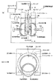
図1(a)は、実施形態に使用される両面研削装置10の構成を示す側面図で、図1(b)は図1(a)のA−A断面図である。
Fig.1 (a) is a side view which shows the structure of the double-sided
同図1に示すように、両面研削装置10は、鉛直方向に立てた姿勢のシリコンウェーハ1の両面1a、1bそれぞれに設けられたパッド11、12と、シリコンウェーハ1の外周部1Rを保護する保護部材としてのキャリア13と、キャリア13を回転駆動させることにより、シリコンウェーハ1を回転させる回転駆動手段としての回転ローラ14と、両パッド11、12の切欠き部11a、12aに位置され、シリコンウェーハの両面1a、1bを挟んで、シリコンウェーハ1の両面1a、1bを研削する研削用砥石15、16と、両パッド11、12に形成された孔からシリコンウェーハ1の両面1a、1bに水を供給する流体供給手段17と、シリコンウェーハ1の一方の面1bを把持してキャリア13にシリコンウェーハ1を装填する(搬入する)とともに、シリコンウェーハ1の一方の面1bを把持してキャリア13から取り出すハンド18と、流体供給手段17とハンド18とを制御して、シリコンウェーハ1の両面研削後に、シリコンウェーハ1の一方の面1aに水を供給することによりシリコンウェーハ1の一方の面1aをパッド11から浮かせつつ、シリコンウェーハ1の他方の面1bを把持することによりキャリア13からシリコンウェーハ1を取り出す制御を行う制御手段としてのコントローラ19とからなる。
As shown in FIG. 1, a double-
パッド12は、図示しないシリンダによって図1(a)の図中左右方向に移動自在である。パッド12を図1(a)の右方向の退避位置に移動させると、ハンド18をパッド11、12間に挿入させることができる。パッド12を図1(a)の左方向の研削位置に移動させると、砥石15、16をそれぞれシリコンウェーハ1の両面1a、1bに接触させることができる。研削位置では、パッド11からシリコンウェーハ1の一方の面1aまでの距離、パッド12からシリコンウェーハ1の他方の面1bまでの距離は、後述する静圧を一定に保つための所定の距離に保持される。
The pad 12 is movable in the left-right direction in FIG. 1A by a cylinder (not shown). When the pad 12 is moved to the retracted position in the right direction in FIG. 1A, the hand 18 can be inserted between the pads 11 and 12. When the pad 12 is moved to the grinding position in the left direction of FIG. 1A, the grindstones 15 and 16 can be brought into contact with both
キャリア13は、シリコンウェーハ1が装填されるリング状の部材であり、シリコンウェーハ1の外周部1Rを保護するために樹脂製で構成されている。キャリア13は、シリコンウェーハ1のノッチ1Nに応じた形状の突起部13aを内周面に備えている。キャリア13の突起部13aをシリコンウェーハ1のノッチ1Nに嵌合させることにより、キャリア13に対してシリコンウェーハ1を位置決めして、保持することができる。キャリア13の厚さは、シリコンウェーハ1の厚さよりも薄く形成されている。
The
キャリア13の外周面には、回転ローラ14、支持ローラ20が接触している。これにより両面研削装置10内でキャリア13が位置決めされる。
The rotating roller 14 and the support roller 20 are in contact with the outer peripheral surface of the
回転ローラ14、支持ローラ20は、シリコンウェーハ1の外周部1Rを保護するために樹脂製で構成されている。
The rotation roller 14 and the support roller 20 are made of resin in order to protect the outer peripheral portion 1R of the
砥石15、16はそれぞれ回転軸15a、15bを備えており、互いに反対方向に回転する。なお、砥石15、16を同じ方向に回転させるように構成してもよい。
The grindstones 15 and 16 have
砥石15、16は、キャリア13内のシリコンウェーハ1の中心1c以下の下方の部位が研削されるように、切欠部11a、12aに位置されている。すなわち、回転ローラ1が駆動されてキャリア13とともにシリコンウェーハ1が回転すると、シリコンウェーハ1の面1a、1bが全面にわたり砥石15、16によって平面研削できるような位置に、砥石15、16が取り付けられている。
The grindstones 15 and 16 are positioned in the notches 11a and 12a so that the lower part below the center 1c of the
図2(a)は、ハンド18の構成図である。ハンド18は、シリコンウェーハ1の一方の面1bを吸着する吸着パッド18aを備えている。ハンド18の吸着パッド18aは、シリコンウェーハ1を保護するために樹脂製で構成されている。
FIG. 2A is a configuration diagram of the hand 18. The hand 18 includes a suction pad 18 a that sucks one
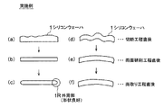
以下、図1の両面研削装置20を用いたシリコンウェーハ1の製造方法について説明する。
Hereinafter, a method for manufacturing the
(第1実施例)
まず、CZ法によって、シリコンインゴットが引上げ成長される。
(First embodiment)
First, a silicon ingot is pulled and grown by the CZ method.
(切断工程)
シリコンインゴットは、ワイヤソー装置によって切断されて、シリコンウェーハ1が取得される。
(Cutting process)
The silicon ingot is cut by a wire saw device, and the
両面研削装置10のパッド12は、図1(a)の右方向の退避位置に移動される。シリコンウェーハ1を把持したハンド18が、パッド11、12間に挿入され、キャリア13にシリコンウェーハ1が装填される(搬入される)。この際に、キャリア13の突起部13aがシリコンウェーハ1のノッチ1Nに嵌合されて、キャリア13に対してシリコンウェーハ1が位置決め、保持される。
The pad 12 of the double-
シリコンウェーハ1の搬入が終わると、パッド12は、図1(a)の左方向の研削位置に移動されて、砥石15、16がそれぞれ、シリコンウェーハ1の両面1a、1bに接触される。
When the carry-in of the
(両面研削工程)
砥石15、16が、互いに反対方向に回転するとともに、回転ローラ14が回転する。これによりシリコンウェーハ1の面1a、1bが全面にわたり砥石15、16によって平面研削される。平面研削中、流体供給手段17は、両パッド11、12に形成された孔からシリコンウェーハ1の両面1a、1bに水を供給して、両パッド11、12間の静圧を所定の値に維持して、シリコンウェーハ1を非接触状態で支持し、鉛直方向に立てた姿勢に保持する。
(Double-side grinding process)
The grindstones 15 and 16 rotate in opposite directions, and the rotating roller 14 rotates. Thereby, the
(ウェーハ取り出し工程(搬出工程))
両面研削加工が終了すると、コントローラ19は、以下のように、流体供給手段17とハンド18とを制御して、シリコンウェーハ1を平面研削装置10から取り出す(搬出する)。
(Wafer unloading process (unloading process))
When the double-side grinding process is completed, the controller 19 controls the fluid supply means 17 and the hand 18 as follows to take out (carry out) the
すなわち、シリコンウェーハ1の両面研削が終了すると、回転ローラ14の回転が停止する。これによりシリコンウェーハ1は、一旦、重力によって下に落ちた状態で回転が停止する。その後、両面研削装置10のパッド12は、図1(a)の右方向の退避位置に移動される。ハンド18が、パッド11、12間に挿入され、シリコンウェーハ1の一方の面1bが、ハンド18の吸着パッド18aによって吸着される。
That is, when the double-side grinding of the
図2(c)に示すように、ハンド18の吸着パッド18aがシリコンウェーハ1の一方の面1bを吸着した状態になると同時に、パッド11の孔からシリコンウェーハ1の一方の面1aに水が供給される。これによりシリコンウェーハ1の一方の面1aがパッド11から浮いた状態となり、この状態でシリコンウェーハ1の他方の面1bをハンド18が把持する。ハンド18によってキャリア13からシリコンウェーハ1を取り出され、平面研削装置1の上方へとシリコンウェーハ1が搬出される。
As shown in FIG. 2 (c), the suction pad 18 a of the hand 18 is in a state of sucking the one
図2(b)は、図2(c)と対比するための比較例であり、流体供給手段17から水を供給しない状態で、シリコンウェーハ1の面1bをハンド18によって把持してキャリア13からシリコンウェーハ1を取り出す場合を示している。
FIG. 2B is a comparative example for comparison with FIG. 2C, and the
図2(b)の比較例の場合には、ハンド18の吸着パッド18aによってシリコンウェーハ1の面1bがパッド11に押し付けられる一方で、シリコンウェーハ1の反対側の面1aには水が供給されないため、シリコンウェーハ1の上部がパッド11に押し付けられ、シリコンウェーハ1の下部が切欠部11aに倒れ込む姿勢となる。このためシリコンウェーハ1の下部がキャリア13に食い込んでしまうことがある。このようにシリコンウェーハ下部がキャリア13に食い込んだ状態のまま、吸着パッド18aによる吸着力がシリコンウェーハ1に作用すると、シリコンウェーハ下部のキャリア13に食い込んだ外周部1Rで、割れが発生するおそれがある。
In the case of the comparative example of FIG. 2B, the
これに対して図2(c)の場合には、シリコンウェーハ1の一方の面1aがパッド11から浮いた状態であるためシリコンウェーハ下部がキャリア13に食い込むことはない。このため、ウェーハ搬出時に、シリコンウェーハ外周部1Rで、欠けやチッピングが発生するおそれはない。
On the other hand, in the case of FIG. 2C, the lower surface of the silicon wafer does not bite into the
また、シリコンウェーハ1の外周部1Rに直接接触する部材、つまりキャリア13、ハンド18をシリコンウェーハ1の外周部1Rを保護する材料(たとえば樹脂製)で構成したので、シリコンウェーハ1の外周部1Rで欠けやチッピングが発生するおそれがない。なお、シリコンウェーハ1の外周部1Rに直接接触する部材(キャリア13、ハンド18)は、シリコンウェーハ1の硬度以下の柔らかい材料であれば、樹脂製以外の任意の材料を使用することができる。
Further, since the members that directly contact the outer peripheral portion 1R of the
(面取り工程)
以上のように両面研削装置1からシリコンウェーハ1が搬出されると、つぎにシリコンウェーハ1の外周部1Rが面取りされる。
(Chamfering process)
When the
図3は、本発明の方法を実施したときのシリコンウェーハ1の断面を模式的に示したものである。
FIG. 3 schematically shows a cross section of the
図3(a)、(b)、(c)はそれぞれ、本実施例の切断工程直後、両面研削工程直後、面取り工程直後のシリコンウェーハ1の断面の形状を示し、図3(d)、(e)、(f)はそれぞれ、本実施例の切断工程直後、両面研削工程直後、面取り工程直後のシリコンウェーハ1の断面のワープ状態を示している。
3 (a), 3 (b), and 3 (c) respectively show the cross-sectional shapes of the
これに対して図4は、本実施例に対する比較例であり、面取り工程後に、両面研削工程を実施したときのシリコンウェーハ1の断面を模式的に示したものである。
On the other hand, FIG. 4 is a comparative example with respect to the present embodiment, and schematically shows a cross section of the
図4(a)、(b)、(c)はそれぞれ、切断工程直後、面取り工程直後、両面研削工程直後のシリコンウェーハ1の断面の形状を示し、図4(d)、(e)、(f)はそれぞれ、切断工程直後、面取り工程直後、両面研削工程直後のシリコンウェーハ1の断面のワープ状態を示している。
4 (a), 4 (b), and 4 (c) show the cross-sectional shapes of the
図4の比較例の場合には、切断工程後のシリコンウェーハ1の反りやうねりが除去されていない状態で面取りが行われるため、面取り後は、シリコンウェーハ1の反りやうねりが残ったままとなる(図4(b)、(e))。この状態で両面研削が実施されと、外周部1Rが不均一に研削されてしまい両面研削工程後のシリコンウェーハ1の外周部1Rの面取り形状が悪化し、ウェーハ周方向での面取り形状がばらつく(図4(c))。
In the case of the comparative example of FIG. 4, since the chamfering is performed in a state where the warp and undulation of the
一方、図3の本実施例の場合には、両面研削工程によって、シリコンウェーハ1の反りやうねりが除去されるとともに、ウェーハ面が平坦化されている状態(図3(b)、(e))で、面取りが実施されるため、面取り工程後のシリコンウェーハ1の外周部1Rの面取り形状は良好なものとなり、ウェーハ周方向での面取り形状は均一でバラツキがないものとなる(図3(c))。
On the other hand, in the case of the present embodiment of FIG. 3, warpage and undulation of the
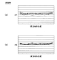
図5(a)は、シリコンウェーハ1の外周部1Rの面取り形状を規定する上面取り幅A1、下面取り幅A2を説明する図である。図5(b)に示すように、シリコンウェーハ1の周方向の各位置で、上面取り幅A1、下面取り幅A2の値が均一でばらつきがなく、しかも上面取り幅A1と下面取り幅A2との差が小さく差が均一でばらつきがないウェーハが理想的である。
FIG. 5A is a diagram for explaining the top chamfering width A1 and the bottom chamfering width A2 that define the chamfering shape of the outer peripheral portion 1R of the
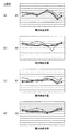
図6(a)、(b)はそれぞれ、図4に示す比較例の場合の面取り工程直後のシリコンウェーハ1の周方向各位置での上面取り幅A1の値、同じく比較例の場合の面取り工程直後のシリコンウェーハ1の周方向各位置での下面取り幅A2の値を、グラフで示している。
FIGS. 6A and 6B are values of the top chamfering width A1 at each position in the circumferential direction of the
図6(c)、(d)はそれぞれ、図4に示す比較例の場合の両面研削工程直後のシリコンウェーハ1の周方向各位置での上面取り幅A1の値、同じく比較例の場合の両面研削工程直後のシリコンウェーハ1の周方向各位置での下面取り幅A2の値を、グラフで示している。
6 (c) and 6 (d) respectively show the value of the top chamfering width A1 at each circumferential position of the
図6(a)、(b)、(c)、(d)は、複数のシリコンウェーハ1についての上面取り幅A1、下面取り幅A2の測定結果を示している。
6A, 6B, 6C, and 6D show the measurement results of the top surface removal width A1 and the bottom surface removal width A2 for a plurality of
図7(a)、(b)はそれぞれ、実施例の場合の面取り工程直後のシリコンウェーハ1の周方向各位置での上面取り幅A1の値、同じく実施例の場合の面取り工程直後のシリコンウェーハ1の周方向各位置での下面取り幅A2の値を、グラフで示している。図7(a)、(b)は、複数のシリコンウェーハ1についての上面取り幅A1、下面取り幅A2の測定結果を示している。
7A and 7B respectively show the values of the top chamfering width A1 at each position in the circumferential direction of the
図8は、比較例(図6(c)、(d))の場合の両面研削工程直後のシリコンウェーハ1の周方向各位置での上面取り幅A1の上限値〜下限値の範囲(バラツキ)とその中心値、下面取り幅A2の上限値〜下限値の範囲(バラツキ)とその中心値と、実施例の場合の面取り工程直後のシリコンウェーハ1の周方向各位置での上面取り幅A1の上限値〜下限値の範囲(バラツキ)とその中心値、下面取り幅A2の上限値〜下限値の範囲(バラツキ)とその中心値とを対比したグラフである。
FIG. 8 shows the range (variation) between the upper limit value and the lower limit value of the top chamfering width A1 at each position in the circumferential direction of the
図6(a)、(b)からわかるように、比較例によれば、切断工程後のシリコンウェーハ1の反りやうねりが除去されていない状態で面取りが行われるため、面取り工程直後は、シリコンウェーハ1の周方向の各位置で、上面取り幅A1、下面取り幅A2の値がばらつくとともに、上面取り幅A1と下面取り幅A2との差が大きく差がばらつく。
As can be seen from FIGS. 6A and 6B, according to the comparative example, chamfering is performed in a state where warpage and undulation of the
また、図6(c)、(d)からわかるように、シリコンウェーハ1の外周部1Rが不均一に研削されるため、面取り工程直後は、シリコンウェーハ1の周方向の各位置で、上面取り幅A1、下面取り幅A2の値がばらつくとともに、上面取り幅A1と下面取り幅A2との差が大きく差がばらつく(図8の比較例A1、A2参照)。
Further, as can be seen from FIGS. 6C and 6D, since the outer peripheral portion 1R of the
これに対して図7(a)、(b)に示すように、本実施例によれば、ウェーハ面が平坦化された状態で、面取りが実施されるため、面取り工程後は、シリコンウェーハ1の周方向の各位置で、上面取り幅A1、下面取り幅A2の値が均一なものとなり、上面取り幅A1と下面取り幅A2との差が小さく、その差が均一でばらつきが少ないものとなる(図8の実施例A1、A2参照)。 On the other hand, as shown in FIGS. 7A and 7B, according to the present embodiment, the chamfering is performed in a state where the wafer surface is flattened. The values of the top chamfering width A1 and the bottom chamfering width A2 are uniform at each circumferential position, the difference between the top chamfering width A1 and the bottom chamfering width A2 is small, the difference is uniform, and there is little variation. (See Examples A1 and A2 in FIG. 8).
以上のように本実施例によれば、シリコンウェーハ1の外周部1Rを保護部材としてのキャリア13によって保護した状態で両面研削を行うようにしたため、両面研削加工を行うことで、シリコンウェーハ1の外周部1Rで欠けやチッピングが生じるようなことがない。また、ウェーハ取り出し工程では、シリコンウェーハ1の一方の面1aに水を供給することによりシリコンウェーハ1の一方の面1aをパッド11から浮かせつつ、シリコンウェーハ1の他方の面1bを把持することによりキャリア13からシリコンウェーハ1を取り出すようにしたので、搬出動作が行われることで、ウェーハ外周部1Rで欠けやチッピングが生じるようなことがない。しかも、本実施例によれば、両面研削工程後に面取り工程を実施しているため、ウェーハ外周部1Rでの面取り形状の悪化、ウェーハ周方向での面取り形状のバラツキをなくすことができる。
As described above, according to the present embodiment, the double-side grinding is performed in a state where the outer peripheral portion 1R of the
(第2実施例)
上述した第1実施例の両面研削工程を、シリコンウェーハ1の両面を粗研削する工程(第1次平面研削)として実施し、面取り工程後に、更にシリコンウェーハ1の両面を仕上げ研削する工程(第2次平面研削)を行うという実施も可能である。
(Second embodiment)
The above-described double-side grinding process of the first embodiment is carried out as a rough grinding process (primary surface grinding) on both sides of the
本実施例によれば、粗研削によってシリコンウェーハ1の大まかな凹凸がすでに除去された状態で面取りが行われるため、面取り後にさらに仕上げ研削を行ったとしても、ウェーハ外周部1Rの面取り形状が損なわれることはない。
According to the present embodiment, the chamfering is performed in a state where the rough unevenness of the
(第3実施例)
また第1実施例の面取り工程を、ウェーハ外周部1Rを本面取りする工程として実施し、両面研削工程の前に、シリコンウェーハ1の外周部1Rを粗面取りする工程を行うという実施も可能である。
(Third embodiment)
In addition, the chamfering process of the first embodiment may be performed as a process of chamfering the outer peripheral part 1R of the wafer, and a process of roughing the outer peripheral part 1R of the
本実施例によれば、粗面取りによって、シリコンウェーハ1の外周部1Rが大まかに面取りされるため、その後のウェーハ搬送時などにおいてウェーハ外周部1Rで欠けやチッピングが生じる可能性がきわめて低くなる。
According to the present embodiment, since the outer peripheral portion 1R of the
なお、上述した説明では、流体供給手段17は、水を供給するものとして説明したが、水以外の液体、空気、各種ガスなどの気体を供給するものであってもよい。 In the above description, the fluid supply means 17 has been described as supplying water, but it may supply liquid such as liquid other than water, air, and various gases.
シリコンウェーハのみならず他のガリウム砒素などの各種半導体ウェーハに面取り加工や両面研削加工を施す場合に本発明を適用することができる。 The present invention can be applied to chamfering and double-side grinding not only on silicon wafers but also on various semiconductor wafers such as gallium arsenide.
1 シリコンウェーハ 10 両面研削装置 13 キャリア 17 流体供給手段 18 ハンド 19 コントローラ
DESCRIPTION OF
Claims (6)
切断工程後に、鉛直方向に立てた姿勢の半導体ウェーハを両パッド間に位置させるとともに半導体ウェーハの外周部を保護部材で保護した状態で保護部材を回転駆動させることにより、半導体ウェーハを回転させて、半導体ウェーハの両面を、研削用砥石を用いて両面研削する両面研削工程と、
両面研削工程後に、半導体ウェーハの一方の面に向けて流体を供給することにより半導体ウェーハの一方の面をパッドから浮かせると同時に半導体ウェーハの他方の面を把持することにより保護部材から半導体ウェーハを取り出す半導体ウェーハ取り出し工程と、
半導体ウェーハ取り出し工程後に、半導体ウェーハの外周部を面取りする面取り工程と
を含むことを特徴とする半導体ウェーハの製造方法。 A cutting step of cutting a semiconductor ingot to obtain a semiconductor wafer;
After the cutting step, the semiconductor wafer is rotated by rotating the protective member in a state where the semiconductor wafer in the vertical position is positioned between both pads and the outer peripheral portion of the semiconductor wafer is protected by the protective member, A double-sided grinding process in which both sides of a semiconductor wafer are ground using a grinding wheel;
After the double-side grinding process, by supplying a fluid toward one surface of the semiconductor wafer, one surface of the semiconductor wafer is lifted from the pad, and at the same time , the other surface of the semiconductor wafer is grasped to take out the semiconductor wafer from the protective member. A semiconductor wafer removal process;
And a chamfering step of chamfering the outer peripheral portion of the semiconductor wafer after the semiconductor wafer removing step.
前記面取り工程後に、半導体ウェーハの両面をさらに研削する工程を実施することを特徴とする請求項1記載の半導体ウェーハの製造方法。 The double-sided grinding step is a step of roughly grinding both sides of a semiconductor wafer,
The method of manufacturing a semiconductor wafer according to claim 1, further comprising a step of grinding both surfaces of the semiconductor wafer after the chamfering step.
を特徴とする含む請求項1記載の半導体ウェーハの製造方法。 The method for manufacturing a semiconductor wafer according to claim 1, wherein a step of rough chamfering the outer peripheral portion of the semiconductor wafer is performed before the double-side grinding step.
両面研削工程後に、半導体ウェーハの一方の面に向けて流体を供給することにより半導体ウェーハの一方の面をパッドから浮かせると同時に半導体ウェーハの他方の面を把持することにより保護部材から半導体ウェーハを取り出す半導体ウェーハ取り出し工程と、
を含むことを特徴とする半導体ウェーハの両面研削方法。 The semiconductor wafer is rotated between the two pads of the semiconductor wafer by rotating the protective member in a state where the vertical position of the semiconductor wafer is positioned between both pads and the outer periphery of the semiconductor wafer is protected by the protective member. A double-sided grinding process in which both sides are ground using a grinding wheel;
After the double-side grinding process, by supplying a fluid toward one surface of the semiconductor wafer, one surface of the semiconductor wafer is lifted from the pad, and at the same time , the other surface of the semiconductor wafer is grasped to take out the semiconductor wafer from the protective member. A semiconductor wafer removal process;
A method for double-sided grinding of a semiconductor wafer, comprising:
鉛直方向に立てた姿勢の半導体ウェーハの両面に設けられたパッドと、
半導体ウェーハの外周部を保護する保護部材と、
保護部材を回転駆動させることにより、半導体ウェーハを回転させる回転駆動手段と、
半導体ウェーハの両面を挟んで、半導体ウェーハの両面を研削する研削用砥石と、
半導体ウェーハの面に流体を供給する流体供給手段と、
半導体ウェーハの面を把持することにより保護部材から半導体ウェーハを取り出す取り出し手段と、
前記流体供給手段と前記取り出し手段とを制御して、半導体ウェーハの両面研削後に、半導体ウェーハの一方の面に向けて流体を供給することにより半導体ウェーハの一方の面をパッドから浮かせると同時に半導体ウェーハの他方の面を把持することにより保護部材から半導体ウェーハを取り出す制御手段と
を備えたことを特徴とする半導体ウェーハの両面研削装置。 A semiconductor wafer double-side grinding apparatus for grinding both sides of a semiconductor wafer,
Pads provided on both sides of a semiconductor wafer in a vertical position;
A protective member for protecting the outer periphery of the semiconductor wafer;
Rotation driving means for rotating the semiconductor wafer by rotating the protective member;
A grinding wheel for grinding both sides of the semiconductor wafer across both sides of the semiconductor wafer,
Fluid supply means for supplying fluid to the surface of the semiconductor wafer;
A take-out means for taking out the semiconductor wafer from the protective member by gripping the surface of the semiconductor wafer;
By controlling the fluid supply means and the take-out means to supply a fluid toward one surface of the semiconductor wafer after both-side grinding of the semiconductor wafer, the semiconductor wafer is lifted from the pad at the same time as the semiconductor wafer. And a control means for taking out the semiconductor wafer from the protective member by gripping the other surface of the semiconductor wafer.
Priority Applications (2)
| Application Number | Priority Date | Filing Date | Title |
|---|---|---|---|
| JP2005152882A JP4798480B2 (en) | 2005-05-25 | 2005-05-25 | Semiconductor wafer manufacturing method, double-sided grinding method, and semiconductor wafer double-sided grinding apparatus |
| TW095112643A TW200731380A (en) | 2005-05-25 | 2006-04-10 | Semiconductor wafer manufacturing method, semiconductor wafer double-sided grinding method, and semiconductor wafer double-sided grinding apparatus |
Applications Claiming Priority (1)
| Application Number | Priority Date | Filing Date | Title |
|---|---|---|---|
| JP2005152882A JP4798480B2 (en) | 2005-05-25 | 2005-05-25 | Semiconductor wafer manufacturing method, double-sided grinding method, and semiconductor wafer double-sided grinding apparatus |
Publications (2)
| Publication Number | Publication Date |
|---|---|
| JP2006332281A JP2006332281A (en) | 2006-12-07 |
| JP4798480B2 true JP4798480B2 (en) | 2011-10-19 |
Family
ID=37553665
Family Applications (1)
| Application Number | Title | Priority Date | Filing Date |
|---|---|---|---|
| JP2005152882A Active JP4798480B2 (en) | 2005-05-25 | 2005-05-25 | Semiconductor wafer manufacturing method, double-sided grinding method, and semiconductor wafer double-sided grinding apparatus |
Country Status (2)
| Country | Link |
|---|---|
| JP (1) | JP4798480B2 (en) |
| TW (1) | TW200731380A (en) |
Families Citing this family (13)
| Publication number | Priority date | Publication date | Assignee | Title |
|---|---|---|---|---|
| JP4985451B2 (en) * | 2008-02-14 | 2012-07-25 | 信越半導体株式会社 | Double-head grinding apparatus for workpiece and double-head grinding method for workpiece |
| JP4780142B2 (en) * | 2008-05-22 | 2011-09-28 | 信越半導体株式会社 | Wafer manufacturing method |
| DE102009025243B4 (en) | 2009-06-17 | 2011-11-17 | Siltronic Ag | Method for producing and method of processing a semiconductor wafer made of silicon |
| JP2011131284A (en) * | 2009-12-22 | 2011-07-07 | Disco Abrasive Syst Ltd | Grinding device |
| JP2013045909A (en) * | 2011-08-25 | 2013-03-04 | Sumco Corp | Method for manufacturing semiconductor wafer |
| JP5872947B2 (en) | 2012-04-05 | 2016-03-01 | 光洋機械工業株式会社 | Work loading / unloading method and double-head surface grinding machine in double-head surface grinding |
| CN109360852A (en) * | 2018-08-14 | 2019-02-19 | 上海芯石微电子有限公司 | A kind of wafer chamfering structure and method reducing chip thinning fragment rate |
| CN114227524A (en) * | 2021-12-30 | 2022-03-25 | 西安奕斯伟材料科技有限公司 | Double-side polishing apparatus and double-side polishing method |
| CN114734319B (en) * | 2022-03-20 | 2023-08-22 | 深圳市陆和神州科技有限公司 | Semiconductor material processing system and method |
| CN114770366B (en) * | 2022-05-17 | 2023-11-17 | 西安奕斯伟材料科技股份有限公司 | Static pressure plate of silicon wafer double-sided grinding device and silicon wafer double-sided grinding device |
| CN115070604B (en) * | 2022-06-09 | 2023-09-29 | 西安奕斯伟材料科技股份有限公司 | Double-sided polishing apparatus and double-sided polishing method |
| CN114986381B (en) * | 2022-06-16 | 2023-08-22 | 西安奕斯伟材料科技股份有限公司 | Double-sided polishing apparatus and double-sided polishing method |
| CN115972078A (en) * | 2022-12-27 | 2023-04-18 | 西安奕斯伟材料科技股份有限公司 | Device and method for double-sided grinding of silicon wafer |
Family Cites Families (5)
| Publication number | Priority date | Publication date | Assignee | Title |
|---|---|---|---|---|
| JPH11154655A (en) * | 1997-11-21 | 1999-06-08 | Komatsu Electron Metals Co Ltd | Manufacture of semiconductor wafer |
| JPH11267964A (en) * | 1998-03-20 | 1999-10-05 | Speedfam Co Ltd | Surface polishing device and carrier used therefor |
| JP2000135670A (en) * | 1998-10-30 | 2000-05-16 | Okamoto Machine Tool Works Ltd | Chemo-mechanical polishing method of wafer |
| JP3951496B2 (en) * | 1999-03-30 | 2007-08-01 | 光洋機械工業株式会社 | Double-side grinding machine for thin disk-shaped workpieces |
| JP2002217147A (en) * | 2001-01-16 | 2002-08-02 | Tokyo Seimitsu Co Ltd | Method and apparatus for recovering wafer for wafer polishing apparatus |
-
2005
- 2005-05-25 JP JP2005152882A patent/JP4798480B2/en active Active
-
2006
- 2006-04-10 TW TW095112643A patent/TW200731380A/en unknown
Also Published As
| Publication number | Publication date |
|---|---|
| TWI353633B (en) | 2011-12-01 |
| JP2006332281A (en) | 2006-12-07 |
| TW200731380A (en) | 2007-08-16 |
Similar Documents
| Publication | Publication Date | Title |
|---|---|---|
| JP4798480B2 (en) | Semiconductor wafer manufacturing method, double-sided grinding method, and semiconductor wafer double-sided grinding apparatus | |
| US9991110B2 (en) | Method for manufacturing semiconductor wafer | |
| EP1755156B1 (en) | Process for producing silicon wafers | |
| JP4758222B2 (en) | Wafer processing method and apparatus | |
| TWI382894B (en) | Silicon wafer grinding method and manufacturing method and disc-like work piece grinding device, and silicon wafer | |
| EP1188516A1 (en) | Method and apparatus for polishing outer peripheral chamfered part of wafer | |
| EP2762272B1 (en) | Wafer polishing apparatus and method | |
| JPH11254309A (en) | Device and method for machining wafer | |
| JP5430975B2 (en) | Work processing method and work processing apparatus | |
| JP2009124153A (en) | Method for producing semiconductor wafer with polished edge part | |
| TWI608897B (en) | Monolithic lapping method for semiconductor wafer and monolithic lapping device for semiconductor wafer | |
| US8092278B2 (en) | Reclamation method of semiconductor wafer | |
| JP2010194680A (en) | Method and apparatus for machining workpiece | |
| JP2013532587A (en) | Grinding tool for trapezoidal grinding of wafers | |
| US6599760B2 (en) | Epitaxial semiconductor wafer manufacturing method | |
| EP3888846A1 (en) | Semiconductor substrate and method for manufacturing same | |
| CN110060959B (en) | Method for manufacturing bonded wafer | |
| TW201236105A (en) | Systems and methods providing an air zone for a chucking stage | |
| JP4103808B2 (en) | Wafer grinding method and wafer | |
| US20080171439A1 (en) | Recycling of ion implantation monitor wafers | |
| JP2001223202A (en) | Method of reducing thickness of semiconductor wafer and device for gliding back face of semiconductor wafer | |
| WO2017082161A1 (en) | Wafer polishing method and device | |
| JP2010040549A (en) | Semiconductor wafer and manufacturing method thereof | |
| JP2010074003A (en) | Grinder and wafer grinding method | |
| KR101151001B1 (en) | Apparatus and method for processing notch of wafer |
Legal Events
| Date | Code | Title | Description |
|---|---|---|---|
| A621 | Written request for application examination |
Free format text: JAPANESE INTERMEDIATE CODE: A621 Effective date: 20080411 |
|
| A977 | Report on retrieval |
Free format text: JAPANESE INTERMEDIATE CODE: A971007 Effective date: 20101006 |
|
| A131 | Notification of reasons for refusal |
Free format text: JAPANESE INTERMEDIATE CODE: A131 Effective date: 20101012 |
|
| A521 | Request for written amendment filed |
Free format text: JAPANESE INTERMEDIATE CODE: A523 Effective date: 20101210 |
|
| A02 | Decision of refusal |
Free format text: JAPANESE INTERMEDIATE CODE: A02 Effective date: 20110308 |
|
| A521 | Request for written amendment filed |
Free format text: JAPANESE INTERMEDIATE CODE: A821 Effective date: 20110607 Free format text: JAPANESE INTERMEDIATE CODE: A523 Effective date: 20110607 |
|
| A911 | Transfer to examiner for re-examination before appeal (zenchi) |
Free format text: JAPANESE INTERMEDIATE CODE: A911 Effective date: 20110614 |
|
| TRDD | Decision of grant or rejection written | ||
| A01 | Written decision to grant a patent or to grant a registration (utility model) |
Free format text: JAPANESE INTERMEDIATE CODE: A01 Effective date: 20110712 |
|
| A01 | Written decision to grant a patent or to grant a registration (utility model) |
Free format text: JAPANESE INTERMEDIATE CODE: A01 |
|
| A521 | Request for written amendment filed |
Free format text: JAPANESE INTERMEDIATE CODE: A821 Effective date: 20110714 |
|
| A61 | First payment of annual fees (during grant procedure) |
Free format text: JAPANESE INTERMEDIATE CODE: A61 Effective date: 20110721 |
|
| FPAY | Renewal fee payment (event date is renewal date of database) |
Free format text: PAYMENT UNTIL: 20140812 Year of fee payment: 3 |
|
| R150 | Certificate of patent or registration of utility model |
Ref document number: 4798480 Country of ref document: JP Free format text: JAPANESE INTERMEDIATE CODE: R150 Free format text: JAPANESE INTERMEDIATE CODE: R150 |
|
| R250 | Receipt of annual fees |
Free format text: JAPANESE INTERMEDIATE CODE: R250 |
|
| R250 | Receipt of annual fees |
Free format text: JAPANESE INTERMEDIATE CODE: R250 |
|
| R250 | Receipt of annual fees |
Free format text: JAPANESE INTERMEDIATE CODE: R250 |
|
| R250 | Receipt of annual fees |
Free format text: JAPANESE INTERMEDIATE CODE: R250 |
|
| R250 | Receipt of annual fees |
Free format text: JAPANESE INTERMEDIATE CODE: R250 |
|
| R250 | Receipt of annual fees |
Free format text: JAPANESE INTERMEDIATE CODE: R250 |
|
| R250 | Receipt of annual fees |
Free format text: JAPANESE INTERMEDIATE CODE: R250 |
|
| R250 | Receipt of annual fees |
Free format text: JAPANESE INTERMEDIATE CODE: R250 |
|
| R250 | Receipt of annual fees |
Free format text: JAPANESE INTERMEDIATE CODE: R250 |
|
| R250 | Receipt of annual fees |
Free format text: JAPANESE INTERMEDIATE CODE: R250 |