JP4788198B2 - Flat display - Google Patents
Flat display Download PDFInfo
- Publication number
- JP4788198B2 JP4788198B2 JP2005154427A JP2005154427A JP4788198B2 JP 4788198 B2 JP4788198 B2 JP 4788198B2 JP 2005154427 A JP2005154427 A JP 2005154427A JP 2005154427 A JP2005154427 A JP 2005154427A JP 4788198 B2 JP4788198 B2 JP 4788198B2
- Authority
- JP
- Japan
- Prior art keywords
- substrate
- reinforcing member
- wiring pattern
- attached
- notch
- Prior art date
- Legal status (The legal status is an assumption and is not a legal conclusion. Google has not performed a legal analysis and makes no representation as to the accuracy of the status listed.)
- Expired - Fee Related
Links
- 239000000758 substrate Substances 0.000 claims description 157
- 230000003014 reinforcing effect Effects 0.000 claims description 120
- 238000005476 soldering Methods 0.000 claims description 14
- 239000000463 material Substances 0.000 claims description 8
- 238000005452 bending Methods 0.000 description 17
- 239000000523 sample Substances 0.000 description 17
- 230000002787 reinforcement Effects 0.000 description 15
- 230000008878 coupling Effects 0.000 description 4
- 238000010168 coupling process Methods 0.000 description 4
- 238000005859 coupling reaction Methods 0.000 description 4
- 238000003780 insertion Methods 0.000 description 4
- 230000037431 insertion Effects 0.000 description 4
- 230000002411 adverse Effects 0.000 description 3
- 238000010586 diagram Methods 0.000 description 3
- 239000004973 liquid crystal related substance Substances 0.000 description 2
- 238000000034 method Methods 0.000 description 2
- 230000002093 peripheral effect Effects 0.000 description 2
- 239000011347 resin Substances 0.000 description 2
- 229920005989 resin Polymers 0.000 description 2
- 238000000926 separation method Methods 0.000 description 2
- RYGMFSIKBFXOCR-UHFFFAOYSA-N Copper Chemical compound [Cu] RYGMFSIKBFXOCR-UHFFFAOYSA-N 0.000 description 1
- 229910052802 copper Inorganic materials 0.000 description 1
- 239000010949 copper Substances 0.000 description 1
- 230000002452 interceptive effect Effects 0.000 description 1
- 229910000679 solder Inorganic materials 0.000 description 1
Images
Landscapes
- Devices For Indicating Variable Information By Combining Individual Elements (AREA)
- Printing Elements For Providing Electric Connections Between Printed Circuits (AREA)
- Structure Of Printed Boards (AREA)
Description
本発明は、フラットディスプレイに関する。 The present invention relates to a flat display.
従来から、フラットディスプレイにおけるパネルの裏面には基板が取り付けられており、この基板には、通常、トランスが実装され、また、各種のコネクタを介してケーブルが接続されるなどしている。このような基板においては、その補強として種々の技術が知られている。例えば、トランスなど重い部品を実装した基板に対する補強部材を基板の端材によって構成する技術が知られている(特許文献1参照。)。
上記従来の補強構造においては、トランスなど重い部品に起因して基板にクラック等が生じることを防止している。しかし、コネクタに対するケーブルの取り付けに起因する不都合を解消することはできなかった。すなわち、コネクタに対してケーブルを取り付ける際にはコネクタを介して基板にテンションがかかるため、補強がなければ基板が撓み、回路内のはんだ付け等に悪影響を及ぼしかねない。また、トランスはその動作に伴って振動し得るが、上記従来の補強構造においてはこの振動に対する対策が採られていないため、振動に伴う音などの発生を防止することができなかった。 In the conventional reinforcing structure, cracks and the like are prevented from occurring on the substrate due to heavy components such as a transformer. However, the inconvenience due to the attachment of the cable to the connector could not be solved. That is, when the cable is attached to the connector, tension is applied to the substrate through the connector, so that there is a possibility that the substrate bends without reinforcement and adversely affects soldering in the circuit. Further, although the transformer can vibrate with its operation, the conventional reinforcing structure does not take measures against this vibration, and thus it has not been possible to prevent the generation of sound and the like accompanying the vibration.
さらに、フラットディスプレイにおいては、その薄さによって付加価値を提供できることから、筐体の後面などできるだけ無駄なスペースを無くすことが望まれており、基板やその周辺のスペースを効率的に利用する必要がある。
本発明は、上記課題にかんがみてなされたもので、コネクタの接続や基板上の部品の振動に対して確実な補強を行い、基板の周りの無駄なスペースを低減することが可能なフラットディスプレイを提供することを目的とする。
Furthermore, since flat displays can provide added value due to their thinness, it is desirable to eliminate as much useless space as possible, such as the rear surface of the chassis, and it is necessary to efficiently use the space around the substrate and its surroundings. is there.
The present invention has been made in view of the above problems, and provides a flat display that can reliably reinforce connection of connectors and vibrations of components on the board, and can reduce useless space around the board. The purpose is to provide.
上記目的の少なくとも一つを達成するため、請求項1の発明は、ケーブルを接続するためのコネクタを備える基板が複数のボスを介して画面表示パネルの裏面に対して取り付けられたフラットディスプレイにおいて、上記基板の端部には切込みおよび当該切込みより内側に設けられた嵌合穴が形成され、上記基板をより大きな基板から切り出す際に生じた端材であるとともに上記基板の切込みに係合するための切込みと上記嵌合穴に嵌合される突起とが形成された補強部材が上記基板の端部に取り付けられており、上記基板と上記画面表示パネルの裏面との間における補強部材の長さは、上記ボスの高さより短く、上記ケーブルを上記コネクタに差し込む際に上記基板が撓むことによって上記補強部材が上記画面表示パネルの裏面に接触するように形成されており、上記基板を挟んで上記ボスと反対側においては上記補強部材にテストピンが形成されるとともに当該テストピンと導通される配線パターンが形成され、上記基板上には上記テストピンと導通されるべき配線パターンが形成されており、上記補強部材を上記基板の端部に取り付けた状態ではんだ付けが行われることで、上記補強部材の配線パターンと上記基板の配線パターンとが導通される構成としてある。 In order to achieve at least one of the above objects, the invention of claim 1 is a flat display in which a substrate having a connector for connecting a cable is attached to the back surface of a screen display panel via a plurality of bosses. A notch and a fitting hole provided on the inner side of the notch are formed at the end of the substrate, which is an end material generated when the substrate is cut out from a larger substrate and engages with the notch of the substrate. A reinforcing member in which a notch and a protrusion that fits into the fitting hole are formed is attached to an end of the substrate, and the length of the reinforcing member between the substrate and the back surface of the screen display panel Is shorter than the height of the boss, and the reinforcing member comes into contact with the back surface of the screen display panel by bending the substrate when the cable is inserted into the connector. A test pin is formed on the reinforcing member and a wiring pattern connected to the test pin is formed on the opposite side of the boss across the substrate, and the test pin is connected to the test pin on the substrate. The wiring pattern to be formed is formed, and the wiring pattern of the reinforcing member and the wiring pattern of the substrate are made conductive by performing soldering in a state where the reinforcing member is attached to the end portion of the substrate. As a configuration.
上記のように構成した請求項1の発明においては、上記基板の端部に切込みおよび当該切込みより内側に設けられた嵌合穴が形成され、上記補強基板には嵌合穴に嵌合する突起と切込みとが形成されている。従って、両者を切込みによって係合させる際に、当該突起が嵌合穴に嵌合し、容易に固定することができる。この結果、基板上の部品やフラットディスプレイ等に振動が生じた場合でも、補強部材の脱落を発生させることがなく、確実に基板を補強することができる。 In the invention of claim 1 configured as described above, a notch and a fitting hole provided inside the notch are formed in the end portion of the substrate, and the protrusion that fits in the fitting hole is formed in the reinforcing substrate. And a notch are formed. Therefore, when engaging both by cutting, the said protrusion fits into a fitting hole, and can be fixed easily. As a result, even when vibration occurs in the components on the substrate, the flat display, or the like, the reinforcing member can be prevented from falling off and the substrate can be reliably reinforced.
また、上記基板と上記画面表示パネルの裏面との間における補強部材の長さは、上記ボスの高さより短い。従って、フラットディスプレイの通常運用時に補強部材と画面表示パネルとが接触することはなく、基板上の部品やフラットディスプレイ等に振動が生じた場合でも、振動音が発生することがない。さらに、上記ケーブルを上記コネクタに差し込む際に上記基板が撓むことによって上記補強部材が上記画面表示パネルの裏面に接触するように形成されているので、ケーブルの差込によって生じる基板の撓みはわずかな撓みに抑えることができ、撓みに起因して回路に悪影響が生じないようにすることができる。 The length of the reinforcing member between the substrate and the back surface of the screen display panel is shorter than the height of the boss. Therefore, the reinforcing member and the screen display panel do not come into contact with each other during normal operation of the flat display, and no vibration noise is generated even when vibration occurs in the components on the substrate, the flat display, or the like. Further, since the reinforcing member is formed so as to come into contact with the back surface of the screen display panel by bending the substrate when the cable is inserted into the connector, the bending of the substrate caused by the insertion of the cable is slight. Therefore, the circuit can be prevented from being adversely affected by the bending.
さらに、上記補強部材と基板とに形成された配線パターンがはんだ付けによって導通されることによって、確実に両者を固定することができる。さらに、補強部材において、上記基板を挟んで上記ボスと反対側(基板面が露出している側)においては、上記配線パターンによって適切な導通が確保されたテストピンが形成されている。このテストピンは基板面が露出している側に配設されることになるので、容易にテストピンに対してプローブを接続することが可能であり、プローブを接続するためのスペースを確保する必要がない。すなわち、テストピンがボス側の基板面上など、プローブを取り付けにくい位置に形成されていると、プローブを取り付けるために大きな作業スペースが必要となるが、本発明のようにボスと反対側において補強部材にテストピンを形成しておけば、容易にプローブを取り付けることができる。従って、必要とされるスペースを節約することができる。 Furthermore, the wiring patterns formed on the reinforcing member and the substrate are made conductive by soldering, so that both can be reliably fixed. Further, in the reinforcing member, on the side opposite to the boss (the side where the substrate surface is exposed) across the substrate, test pins in which appropriate conduction is ensured by the wiring pattern are formed. Since this test pin is arranged on the side where the board surface is exposed, it is possible to easily connect the probe to the test pin, and it is necessary to secure a space for connecting the probe. There is no. In other words, if the test pin is formed at a position where it is difficult to attach the probe, such as on the board surface on the boss side, a large work space is required to attach the probe. If a test pin is formed on the member, the probe can be easily attached. Therefore, the required space can be saved.
また、本発明の態様の1つは、ケーブルを接続するためのコネクタを備える基板が複数のボスを介して画面表示パネルの裏面に対して取り付けられたフラットディスプレイにおいて、上記基板には切込みが形成され、上記基板をより大きな基板から切り出す際に生じた端材であるとともに上記基板の切込みに係合するための切込みが形成された補強部材が上記基板に取り付けられており、上記補強部材は上記ケーブルを上記コネクタに差し込む際の上記基板の撓みを抑える構成としてある。 Also, one aspect of the present invention is a flat display in which a substrate having a connector for connecting a cable is attached to the back surface of the screen display panel through a plurality of bosses, and the substrate is notched. And a reinforcing member which is an end material generated when the substrate is cut out from a larger substrate and is formed with a notch for engaging with the notch of the substrate, is attached to the substrate, and the reinforcing member is In this configuration, the board is prevented from bending when the cable is inserted into the connector.
上記のように構成した本発明の態様の1つにおいて、補強部材は、基板を切り出す際に生じる端材を利用して作成される。従って、コストを抑えることができる。また、基板と補強部材とには切込みが形成されており、この切込みを利用して基板と補強部材とを係合させる。これにより、補強部材を基板に対して容易に取り付けることができる。また、基板と補強部材とに切込みを入れるのみで補強部材の取り付けを可能にしているので、基板に対して取り付け可能な補強部材を非常に容易に形成することができる。 In one of the aspects of the present invention configured as described above, the reinforcing member is created by using an end material generated when the substrate is cut out. Therefore, the cost can be suppressed. In addition, a cut is formed in the substrate and the reinforcing member, and the substrate and the reinforcing member are engaged using this cut. Thereby, a reinforcement member can be easily attached with respect to a board | substrate. Further, since the reinforcing member can be attached only by making a cut in the substrate and the reinforcing member, the reinforcing member that can be attached to the substrate can be formed very easily.
さらに、この補強部材は、上記ケーブルを上記コネクタに差し込む際の上記基板の撓みを抑えるように取り付けられる。すなわち、基板はボスを介して取り付けられるため、取り付けを行った状態であってもボスの中間に近いほど基板は撓み易い。そこで、本発明ではこの撓みを抑えるように補強部材を取り付けている。この結果、ケーブルをコネクタに差し込む際に基板を撓ませる力が作用したとしても、その結果基板に生じる撓みを抑えることができる。 Further, the reinforcing member is attached so as to suppress bending of the board when the cable is inserted into the connector. That is, since the substrate is attached through the boss, the substrate is more easily bent as it is closer to the middle of the boss even in the attached state. Therefore, in the present invention, a reinforcing member is attached so as to suppress this bending. As a result, even when a force that bends the board is applied when the cable is inserted into the connector, the resulting bending of the board can be suppressed.
尚、補強部材は、ケーブルを上記コネクタに差し込む際の上記基板の撓みを抑えられる位置に取り付けることができればよい。従って、コネクタ付近に取り付けるよう構成してもよいし、上記ボスの中間付近に取り付けるように構成してもよい。また、基板に対して接続するコネクタは、基板の端部に形成されることが多いので、この場合は、基板の端部に切込みを入れるのみでよく、非常に容易に本発明を構成することができる。また、フラットディスプレイの形式は特に限定されず、プラズマディスプレイパネル、液晶ディスプレイパネルやSEDパネル、有機ELパネルなど、種々の画面表示パネルを利用するフラットディスプレイに本発明を適用することができる。 The reinforcing member only needs to be attached at a position where bending of the substrate when the cable is inserted into the connector can be suppressed. Therefore, it may be configured to be mounted near the connector, or may be configured to be mounted near the middle of the boss. In addition, since the connector connected to the board is often formed at the end of the board, in this case, it is only necessary to make a notch at the end of the board, and the present invention can be configured very easily. Can do. The form of the flat display is not particularly limited, and the present invention can be applied to a flat display using various screen display panels such as a plasma display panel, a liquid crystal display panel, an SED panel, and an organic EL panel.
さらに、補強部材は、ケーブルをコネクタに差し込む際の基板の撓みを抑えることができればよいので、このための構成に加えて振動音の発生を防止する構成を採用することが好ましい。このために、上記基板と上記画面表示パネルの裏面との間における補強部材の長さは、上記ボスの高さより短く、上記ケーブルを上記コネクタに差し込む際に上記基板が撓むことによって上記補強部材が上記画面表示パネルの裏面に接触するように形成されている構成としてもよい。 Furthermore, the reinforcing member only needs to be able to suppress the bending of the substrate when the cable is inserted into the connector, and therefore it is preferable to employ a configuration that prevents the generation of vibration noise in addition to the configuration for this purpose. For this, the length of the reinforcing member between the rear surface of the upper Symbol substrate and the screen display panel is shorter than the height of the boss, the reinforcement by the substrate is bent when inserting the cable into the connector It is good also as a structure currently formed so that a member may contact the back surface of the said screen display panel.
すなわち、基板はボスを介して取り付けられるので、基板と画面表示パネルとの間には当該ボスの高さと略同じ距離の間隔が生じている。そこで、補強部材を取り付けたときに基板と画面表示パネルとの間に存在する補強部材の長さを当該ボスの高さより小さくするとともに、コネクタに対するケーブルの差込によって基板が撓む場合には撓み量が小さいうちに補強部材と画面表示パネルとが接触するように構成する。 That is, since the substrate is attached via the boss, an interval of approximately the same distance as the height of the boss is generated between the substrate and the screen display panel. Therefore, when the reinforcing member is attached, the length of the reinforcing member existing between the board and the screen display panel is made smaller than the height of the boss, and the board is bent when the board is bent by inserting the cable into the connector. The reinforcing member and the screen display panel are in contact with each other while the amount is small.
この結果、フラットディスプレイの通常動作によって基板が振動したとしても、その振動によって補強部材が画面表示パネルに接触することはなく、振動音が発生することはない。尚、ここでは、振動によって補強部材が画面表示パネルに接触しないように構成する必要があるので、無振動時に補強部材と画面表示パネルとの離間距離を当該振動による振動幅以上にすることになる。また、コネクタに対するケーブルの差込によって基板が撓む場合に補強部材が画面表示パネルに接触するよう構成するので、上記離間距離は、上記振動幅以上である限りにおいてできるだけ小さい距離であることが好ましい。 As a result, even if the substrate vibrates due to the normal operation of the flat display, the reinforcing member does not come into contact with the screen display panel due to the vibration, and no vibration sound is generated. In addition, since it is necessary to comprise so that a reinforcement member may not contact a screen display panel by vibration here, the separation distance of a reinforcement member and a screen display panel shall be more than the vibration width by the said vibration at the time of no vibration. . Further, since the reinforcing member is configured to come into contact with the screen display panel when the board is bent by inserting the cable into the connector, the separation distance is preferably as small as possible as long as it is equal to or greater than the vibration width. .
さらに、基板と補強部材とを確実に結合する構成を採用してもよく、上記基板と上記補強部材のいずれか一方には上記切込みより内側に嵌合穴が形成され、他方には当該嵌合穴に嵌合される突起が形成されている構成としてもよい。すなわち、基板と補強部材とを切込み同士の嵌合のみによって結合させるのではなく、この結合に加え、嵌合穴と突起との嵌合も併用して結合する。この結果、突起が嵌合穴から脱落しない限り基板と補強部材との結合が解除されることはなくなり、簡易な構成によって確実に補強部材を取り付ける構成を提供することができる。 Furthermore, may be employed a configuration to reliably bond the substrate and the reinforcing member, the fitting hole on the inner side than the cut is formed in either the upper Symbol substrate and the reinforcing member, the fitting to the other It is good also as a structure in which the protrusion fitted to a fitting hole is formed. That is, the substrate and the reinforcing member are not coupled by only fitting the cuts, but in addition to this coupling, the coupling between the fitting hole and the protrusion is also used in combination. As a result, the connection between the substrate and the reinforcing member is not released unless the protrusions are removed from the fitting holes, and a configuration in which the reinforcing member is securely attached with a simple configuration can be provided.
さらに、切込みによって基板と補強部材とを結合させる構成としては種々の構成を採用可能であり、上記補強部材の一部には切込みによって他の部位より細い回転軸部が形成されており、上記基板の切込みは当該補強部材を挿入するとともに上記回転軸部を中心に回転可能な大きさの穴である構成としてもよい。すなわち、補強部材を基板の穴に挿入し、ねじることによって補強部材と基板とを係合させる。このために、補強部材には他の部位より細いくびれた部分を形成しておき、このくびれた部分を回転軸として回転させる。この結果、補強部材は基板の穴から脱落することがなくなる。また、この構成においては、非常に容易に補強部材を基板に取り付けることが可能である。 Further, a structure for coupling the substrate and the reinforcing member by a cut is possible to employ various configurations, a part of the upper Symbol reinforcing member is thin rotating shaft portion than the other portions is formed by a notch, the The notch of the substrate may be a hole having a size that allows the reinforcing member to be inserted and can be rotated around the rotation shaft portion. That is, the reinforcing member is inserted into the hole of the substrate and twisted to engage the reinforcing member with the substrate. For this purpose, a narrower part than the other part is formed in the reinforcing member, and the constricted part is rotated as a rotation axis. As a result, the reinforcing member does not fall out of the hole in the substrate. In this configuration, the reinforcing member can be attached to the substrate very easily.
さらに、上記基板と補強部材とには両者をはんだ付けによって固定するための配線パターンが形成されている構成としてもよい。すなわち、はんだ付けを用いることによって基板と補強部材とを強固に結合することができる。尚、基板においては、通常、はんだをはじく樹脂が塗布されているので、ここでは、配線パターンを形成し、当該配線パターンを露出させることとし、当該露出させた部位によってはんだ付けを行う構成とする。 Furthermore, it may be both in the upper Symbol substrate and reinforcement member a structure in which a wiring pattern for fixing by soldering are formed. That is, the substrate and the reinforcing member can be firmly bonded by using soldering. In addition, since a resin that repels solder is usually applied to the substrate, here, a wiring pattern is formed, the wiring pattern is exposed, and soldering is performed by the exposed portion. .
さらに、基板の周りのスペースを節約するための構成を採用してもよく、上記補強部材にはテストピンが形成されるとともに上記補強部材の配線パターンに導通されており、上記基板の配線パターンは当該テストピンと導通されるべき部位に導通されている構成としてもよい。すなわち、テストピンは、基板に形成される回路の任意の部位における電位(グラウンドや電源等)が所定の電位であるか否かをチェックするための接点となるピンであり、通常は、細いピンに対してプローブを接続して電位をチェックする。 Further, by adopting the configuration to save space around the substrate rather it may also have been conducted to the wiring pattern of the reinforcing member together with a test pin to the reinforcing member is formed, the substrate wiring pattern it may be a configuration that is conducted to the site to be conducted to the test pin. In other words, the test pin is a pin that serves as a contact point for checking whether or not the potential (ground, power supply, etc.) at any part of the circuit formed on the substrate is a predetermined potential. Connect the probe to and check the potential.
そこで、当該プローブを接続するためのピンを補強部材に形成し、テストピンと導通させるべき部位に配線するように基板と補強部材とに配線パターンを形成する。この結果、基板の面から離れた位置にてプローブとテストピンとを接続することができ、基板上にたくさんの部品が実装されているとしても、プローブを容易に取り付けることができる。従って、プローブを取り付けるための作業スペースを考慮することなく、基板や画面表示パネル等の配置を決定することができ、基板の周りの無駄なスペースを低減することができる。 Therefore, a pin for connecting the probe is formed on the reinforcing member, and a wiring pattern is formed on the substrate and the reinforcing member so as to be wired to a portion to be electrically connected to the test pin. As a result, the probe and the test pin can be connected at a position away from the surface of the substrate, and the probe can be easily attached even if many components are mounted on the substrate. Therefore, it is possible to determine the arrangement of the substrate, the screen display panel, and the like without considering the work space for attaching the probe, and it is possible to reduce the useless space around the substrate.
さらに、上記補強部材には、上記ケーブルを架けるための切欠が形成されている構成としてもよい。すなわち、ケーブルを架けることによって基板周りのケーブルを整理して組み立てを行うことが可能になり、基板の周りの無駄なスペースを低減して容易に組み立てが可能なフラットディスプレイを構成することができる。 Further, the upper Symbol reinforcing member may be configured to notch for applying the cable is formed. That is, it is possible to organize and assemble cables around the board by laying the cables, and it is possible to configure a flat display that can be easily assembled by reducing useless space around the board.
以上説明したように、請求項1にかかる発明によれば、基板と補強部材とを容易に結合し、しかも脱落を防止することができる。また、基板の振動に起因する振動音の発生を防止することができる。さらに、コネクタの差込に伴う基板の撓みを抑えることが可能である。さらに、テストピンに対して容易にプローブを取り付けられ、プローブによる作業のためのスペースを節約することができる。 As described above, according to the first aspect of the present invention, the substrate and the reinforcing member can be easily coupled and can be prevented from falling off. In addition, it is possible to prevent generation of vibration sound due to the vibration of the substrate. Furthermore, it is possible to suppress the bending of the board accompanying the insertion of the connector. Further, the probe can be easily attached to the test pin, and the space for working with the probe can be saved .
ここでは、下記の順序に従って本発明の実施の形態について説明する。
(1)プラズマディスプレイの概略構成:
(2)基板および補強部材の構成:
(3)他の実施形態:
Here, embodiments of the present invention will be described in the following order.
(1) Schematic configuration of plasma display:
(2) Configuration of substrate and reinforcing member:
(3) Other embodiments:
(1)プラズマディスプレイの概略構成:
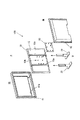
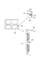
図1は、本願にかかるフラットディスプレイの分解斜視図である。本明細書では、プラズマディスプレイをフラットディスプレイの例として説明するが、むろん、液晶ディスプレイやSED,有機ELなど各種のフラットディスプレイに本発明を適用することが可能である。
同図に示すように、プラズマディスプレイ100は、概略、プラズマディスプレイパネル(PDP)10と、枠体30とフロントキャビネット41とリアキャビネット42とを組立てることによって構成される。PDP10には、その後面(裏面)側の所定箇所において図示しないアタッチメントを介してブラケット10aが取り付けられている。当該ブラケット10aはさらに、上記に枠体30に対して固定されている。
(1) Schematic configuration of plasma display:
FIG. 1 is an exploded perspective view of a flat display according to the present application. In this specification, a plasma display will be described as an example of a flat display. However, it is needless to say that the present invention can be applied to various flat displays such as a liquid crystal display, SED, and organic EL.
As shown in the figure, the
フロントキャビネット41の前面の略中央には、開口41aが形成されており、PDP10は、上記ブラケット10aおよび枠体30に取り付けられた状態で、その前面を同開口41aに向けてキャビネット内に配設される。すなわち、PDP10の前面側にはフロントキャビネット41が取り付けられ、PDP10の後面側には、リアキャビネット42が取り付けられる。また、PDP10の下側には、足部材20が取り付けられる。
An
PDP10の後面には複数のボス10bが形成されている。ボス10bは、図1において簡略化して示す基板50のねじ穴に対応した位置に形成されており、当該ねじ穴にねじを挿入しつつボス10bにねじを螺合することで基板50をPDP10の後面側に固定する。
A plurality of
(2)基板および補強部材の構成:
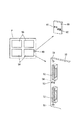
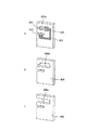
図2は、基板50と当該基板50を補強するための補強部材60とを説明する説明図である。本実施形態において、基板50には、上記ボス10bに対応した位置にねじ穴51が形成されており、基板50の端部に複数のコネクタ52が設けられている。コネクタ52の近辺(本実施形態においては2つのコネクタ52の間)には、切込み53が形成されている。当該切込み53は基板50の端部に形成されている。尚、図2は簡略化して示しているが、基板50はPDP10の電源回路が実装されており、コネクタ52が実装されている面に図示しないトランス等を備えている。
(2) Configuration of substrate and reinforcing member:
FIG. 2 is an explanatory diagram for explaining the
本実施形態において、基板50はより大きな基板Pから切り出されており、同じ大きさの複数の基板が切り出される。このとき、各基板50の端部に隣接していた部位は端材となるが、本実施形態においてはこの端材から補強部材60を形成している。補強部材60は略矩形であるとともにその端部に上記基板50の切込み53と略同じ長さの切込み61が形成されている。基板50の切込み53と補強部材60の切込み61とは、双方とも基板の厚さと略同じ長さの幅である。従って、切込み53と切込み61とを係合させながら補強部材60を基板50に取り付けることができる。
In the present embodiment, the
また、補強部材60には配線パターンが形成されており、その一面において切込み61より下側には配線パターン露出部62が形成されている。基板50においては、補強部材60を基板50に取り付けた状態において当該配線パターン露出部62に対応する位置に配線パターン露出部54が形成されている。すなわち、各露出部には予め銅の配線パターンが形成されており、この部位は樹脂で覆われていない。従って、配線パターン露出部62と配線パターン露出部54とをはんだ付けすることによって基板50と補強部材60とを結合することができる。尚、図2においては、基板50の裏面に配線パターン露出部54が形成されていることを破線によって示している。
In addition, a wiring pattern is formed on the reinforcing
図3は、基板50をPDP10に取り付け、補強部材60を基板50に取り付けた状態を基板50の面に平行な方向から眺めた場合の図を示している。基板50のねじ穴51には、同図に示すようにねじ51aが挿入され、このねじ51aがPDP10に立設するボス10bに螺合する。この結果、基板50はPDP10の後面側に取り付けられる。補強部材60が基板50に取り付けられる際には、上述のように配線パターン露出部62と配線パターン露出部54とにはんだ付け63が施される。
FIG. 3 shows a view in which the
本実施形態において、補強部材60の切込み61より下の部分は図3において基板50の下面とPDP10との間に位置することになるが、この部分の長さLはボス10bの高さより短くなっている。また、補強部材60の下端部とPDP10との間に形成された間隔lは、基板50上に実装されるトランス等による振動に起因した基板50の振動幅より大きくなっている。従って、基板50上に実装される部品等に起因して基板50が振動したとしても、補強部材60の下端部がPDP10に接触することはなく、補強部材60の下端部がPDP10に接触することによる振動音は発生しない。
In the present embodiment, the portion below the
また、プラズマディスプレイ100の組み立てにおいては、基板50がボス10bに取り付けられた状態でコネクタ52に所定のケーブルを接続する。このとき、ケーブルのコネクタは基板50のコネクタ52に対して図3の紙面上側から下側に向けて差し込まれる。従って、基板50には下側に向けた力が作用し、この力によって基板50は下側に向けて撓もうとする。
In assembling the
基板50が撓むと、この撓みに伴って補強部材60も下に移動するが、補強部材60の下端部とPDP10との間には距離lが開いているのみであるので、撓み量がlとなった時点で補強部材60とPDP10とが干渉する。従って、基板50の撓み量がlを超えることはなく、撓み量はわずかである。このため、ケーブルの差込によって、基板50の回路等に悪影響を及ぼし得る撓みが発生しないように、確実な補強を行うことができる。
When the
以上のように、本実施形態においては、補強部材60を端材によって構成し、基板50のコネクタ52の付近に切込みを設けるのみで両者を結合することができるので、低コストでケーブルをコネクタに差し込む際の基板の撓みを抑える構造を提供することができる。さらに、補強部材60の長さを調整することによって、通常では補強部材60とPDP10が接触しないが、コネクタ52に対するケーブルの接続時には補強部材60とPDP10が接触するように構成している。従って、振動音の発生を抑えながら、確実に基板50の撓みを防止することができる。
As described above, in the present embodiment, the reinforcing
(3)他の実施形態:
上記実施形態は一例であり、本発明においては、ケーブルの差込に伴う基板の撓みを防止することができる限りにおいて、種々の構成を採用可能である。例えば、基板50と補強部材60とに設ける切込み部分の形状によってより確実に両者を取り付けるための構成を採用してもよい。
(3) Other embodiments:
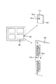
The above embodiment is merely an example, and various configurations can be employed in the present invention as long as the board can be prevented from being bent due to the insertion of the cable. For example, you may employ | adopt the structure for attaching both more reliably with the shape of the notch part provided in the board |
図4は、このための構成を説明する説明図であり、補強部材601の概略形状と基板501の構成内容とは上記実施形態とほぼ同様である。但し、切込み部分の構成は異なっており、補強部材601においては、切込み611の端部において互いに対向する突起611aが形成してある。すなわち、切込み611の端部(補強部材601の外周側)においては、一部で幅が狭くなるように切込み611が形成されている。
FIG. 4 is an explanatory diagram for explaining the configuration for this purpose, and the schematic shape of the reinforcing
基板501においては、切込み531が形成されるとともに、その内側(基板501の外周と逆側)に嵌合穴531aが形成されている。当該嵌合穴531aの位置は、切込み611,531を利用して上記補強部材601を基板501に取り付けたときに突起611aが位置する部分に相当する。従って、切込み611を利用して補強部材601を基板501の切込み531に挿入していくと、奥まで挿入した時点で突起611aが嵌合穴531aに嵌合する。
In the
従って、補強部材601と基板501とが強固に結合され、補強部材601が基板501から容易に脱落しないような構成とすることができる。尚、図4に示す実施形態においては、突起611aと嵌合穴531aとの嵌合によって補強部材601と基板501とが結合されるため、配線パターン露出部を省略してはんだ付けを行わない場合を想定しているが、むろん、より確実な結合を行うために、配線パターン露出部を設けてはんだ付けを行ってもよい。また、図4に示す突起611aや嵌合穴531aの位置や大きさは特に限定されず、両者の嵌合によって補強部材601と基板501との結合を強固にすることができる限りにおいて種々の構成を採用可能である。
Therefore, the reinforcing
さらに、補強部材と基板との形状は上記実施形態のような形状に限定されることはない。図5は、このための構成を説明する説明図である。ここでも基板502の構成内容とは上記実施形態とほぼ同様であるが補強部材602の概略形状と切込み部分の構成は異なっている。補強部材602においては、その外周側から内側に向かって2つの切込み612が形成されている。さらに、この切込みの間に形成される括れ612aの幅は、後述する矩形穴532の幅と略同一になるように形成してある。
Furthermore, the shape of the reinforcing member and the substrate is not limited to the shape as in the above embodiment. FIG. 5 is an explanatory diagram for explaining the configuration for this purpose. Here, the configuration content of the
また、基板502においては、矩形穴(切込み)532が形成されており、この矩形穴の内周は補強部材602を挿入可能な大きさに形成してある。従って、基板502の面に垂直な方向に補強部材602を立てるように配向させながら、補強部材602を基板502の矩形穴532に挿入することができる。
In addition, a rectangular hole (cut) 532 is formed in the
補強部材602を矩形穴532に挿入し、切込み612が矩形穴532に達している状態で上記括れ612aを軸中心にして補強部材602をねじると当該補強部材602は回転する。このとき、基板502が補強部材602における切込み612の上部分と下部分に挟まれ、補強部材602を基板502に対して固定することができる。
When the reinforcing
尚、本実施形態においても補強部材602に配線パターン露出部622が形成されており、基板502に配線パターン露出部542が形成されているので、はんだ付けによって補強部材602と基板502とを確実に結合させることができる。むろん、ここでも補強部材602や矩形穴532の大きさや形状が限定されることはなく、括れ612aをより大きくし、この括れを回転させることができるように矩形穴532に幅広の部位を設けるなど、種々の構成を採用可能である。
Also in the present embodiment is formed with a wiring pattern exposed
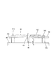
さらに、補強部材の形状等を工夫することによって、より便利な機能を提供することも可能である。図6Aは、補強部材603にテストピン633を設けた例を示している。すなわち、補強部材603の概形は上記図2に示す補強部材60とほぼ同様であるが、補強部材603においては、その一面にテストピン633が取り付けられている。テストピンは、電源やグラウンドなど、回路内の予め決められた箇所に接続され、その箇所の電位を測定するためのピンである。
Furthermore, a more convenient function can be provided by devising the shape or the like of the reinforcing member. FIG. 6A shows an example in which a
そこで、補強部材603においては、テストピン633を形成するとともに当該テストピン633の足部分に予め配線パターン623を形成しておく。従って、テストピン633と配線パターン623とは導通する。尚、本実施形態においては、テストピン633の中央部分に相当する位置に穴633aが形成されており、この穴によってプローブの先端が補強部材603と干渉することを防止している。また、この例において、配線パターン623は切込み613の下方を回り込み、切込み613の直下まで配線されている。また、少なくとも切込み613の直下では配線パターンが露出されている。
Therefore, in the reinforcing
従って、この補強部材603が取り付けられる図示しない基板においては切込み613の直下に配線パターンが露出されており、はんだ付けによって配線パターンの導通が確保される。むろん、はんだ付けされる配線パターンはテストピン633による検査対象の部位に導通されている。従って、この実施形態においては、はんだ付けによって補強部材603と基板とを確実に接続することが可能であり、さらに、テストピン633に対してプローブを容易に接続することが可能である。
Therefore, on the substrate (not shown) to which the reinforcing
テストピン633は、一般に小さな部品であり、基板上の実装部品は多数になることが多い。従って、基板上にテストピンが形成されているとしても、プローブを接続しづらければ、作業効率が落ちてしまう。しかし、本実施形態においては、テストピン633が基板の面より上方に位置し、また、補強部材603の存在によって容易に見つけることができる。さらに、補強部材603に形成した穴633aによってプローブを容易にテストピン633に装着することができる。従って、プローブをテストピン633に接続するための作業が非常に容易であり、特別に作業スペースを設ける必要がないので、プラズマディスプレイ100をより薄くすることが可能である。
The
さらに、図6B,図6Cに示すように、補強部材604,605の上部に切欠604a,605aを設けてもよい。補強部材604,605は基板上のコネクタ付近に取り付けられるが、コネクタに対して接続するケーブルが増加すれば、ケーブルを整理して効率的に配置する必要が生じる。そこで、ケーブルを切欠604a,605aに架ければケーブルの配置を安定させることができ、その取り回しが非常に容易になる。従って、ケーブルを配設するために余分なスペースを設ける必要がなくなり、プラズマディスプレイ100を可能な限り薄くすることが可能になる。また、取り回しが容易になるため、プラズマディスプレイ100の組み立てが非常に容易になる。
Further, as shown in FIGS. 6B and 6C,
10…PDP
10a…ブラケット
10b…ボス
20…足部材
30…枠体
41…フロントキャビネット
41a…開口
42…リアキャビネット
50…基板
51…ねじ穴
52…コネクタ
53…切込み
54…配線パターン露出部
60…補強部材
61…切込み
62…配線パターン露出部
63…はんだ付け
10 ... PDP
DESCRIPTION OF
Claims (1)
上記基板の端部には切込みおよび当該切込みより内側に設けられた嵌合穴が形成され、
上記基板をより大きな基板から切り出す際に生じた端材であるとともに上記基板の切込みに係合するための切込みと上記嵌合穴に嵌合される突起とが形成された補強部材が上記基板の端部に取り付けられており、
上記基板と上記画面表示パネルの裏面との間における補強部材の長さは、上記ボスの高さより短く、上記ケーブルを上記コネクタに差し込む際に上記基板が撓むことによって上記補強部材が上記画面表示パネルの裏面に接触するように形成されており、
上記基板を挟んで上記ボスと反対側においては上記補強部材にテストピンが形成されるとともに当該テストピンと導通される配線パターンが形成され、上記基板上には上記テストピンと導通されるべき配線パターンが形成されており、上記補強部材を上記基板の端部に取り付けた状態ではんだ付けが行われることで、上記補強部材の配線パターンと上記基板の配線パターンとが導通されることを特徴とするフラットディスプレイ。 In a flat display in which a substrate having a connector for connecting a cable is attached to the back surface of the screen display panel via a plurality of bosses,
The end of the substrate is formed with a notch and a fitting hole provided inside the notch,
A reinforcing member which is an end material generated when the substrate is cut out from a larger substrate and has a notch for engaging with the notch of the substrate and a protrusion to be fitted into the fitting hole is formed on the substrate. Attached to the end,
The length of the reinforcing member between the substrate and the back surface of the screen display panel is shorter than the height of the boss. When the cable is inserted into the connector, the substrate is bent to cause the reinforcing member to display the screen. It is formed to contact the back of the panel,
On the opposite side of the boss across the substrate, a test pin is formed on the reinforcing member and a wiring pattern is formed to be electrically connected to the test pin. A wiring pattern to be electrically connected to the test pin is formed on the substrate. A flat, wherein the wiring pattern of the reinforcing member is electrically connected to the wiring pattern of the substrate by performing soldering in a state where the reinforcing member is attached to the end portion of the substrate. display.
Priority Applications (1)
| Application Number | Priority Date | Filing Date | Title |
|---|---|---|---|
| JP2005154427A JP4788198B2 (en) | 2005-05-26 | 2005-05-26 | Flat display |
Applications Claiming Priority (1)
| Application Number | Priority Date | Filing Date | Title |
|---|---|---|---|
| JP2005154427A JP4788198B2 (en) | 2005-05-26 | 2005-05-26 | Flat display |
Publications (2)
| Publication Number | Publication Date |
|---|---|
| JP2006330396A JP2006330396A (en) | 2006-12-07 |
| JP4788198B2 true JP4788198B2 (en) | 2011-10-05 |
Family
ID=37552139
Family Applications (1)
| Application Number | Title | Priority Date | Filing Date |
|---|---|---|---|
| JP2005154427A Expired - Fee Related JP4788198B2 (en) | 2005-05-26 | 2005-05-26 | Flat display |
Country Status (1)
| Country | Link |
|---|---|
| JP (1) | JP4788198B2 (en) |
Family Cites Families (6)
| Publication number | Priority date | Publication date | Assignee | Title |
|---|---|---|---|---|
| JPH074784B2 (en) * | 1985-12-12 | 1995-01-25 | 豊田工機株式会社 | Robot hand |
| JP3347569B2 (en) * | 1996-03-04 | 2002-11-20 | キヤノン株式会社 | Flat plate type image forming apparatus |
| JP2001267697A (en) * | 2000-03-21 | 2001-09-28 | Aiwa Co Ltd | Reinforcement member in board and mounting method |
| JP2001332886A (en) * | 2000-05-22 | 2001-11-30 | Matsushita Electric Ind Co Ltd | Shield housing |
| JP2003283060A (en) * | 2002-03-27 | 2003-10-03 | Oki Electric Ind Co Ltd | Card package mounting inserting side connector half |
| KR100683739B1 (en) * | 2004-12-15 | 2007-02-20 | 삼성에스디아이 주식회사 | Plasma display device |
-
2005
- 2005-05-26 JP JP2005154427A patent/JP4788198B2/en not_active Expired - Fee Related
Also Published As
| Publication number | Publication date |
|---|---|
| JP2006330396A (en) | 2006-12-07 |
Similar Documents
| Publication | Publication Date | Title |
|---|---|---|
| JP2933845B2 (en) | Printed circuit board mounting device | |
| JP5289712B2 (en) | Shield cover mounting structure and display device | |
| JP2006195457A (en) | Plasma display device | |
| JP2011048732A (en) | Electronic apparatus | |
| JP6076217B2 (en) | Substrate fixing structure and electronic device to which the substrate fixing structure is applied | |
| JP4884334B2 (en) | Image display device | |
| JP4483258B2 (en) | Connector-integrated printed circuit board connection structure | |
| JP4788198B2 (en) | Flat display | |
| CN103730743A (en) | Electronic device, method for manufacturing same, and flexible printed circuit board | |
| JP3925097B2 (en) | PCB mounting structure | |
| JP2006108387A (en) | Flexible printed circuit board reinforcement structure | |
| JP2012133933A (en) | Flexible substrate, semiconductor device, and image display unit using the same | |
| JP4385341B2 (en) | Connector parts, connector systems, and electronic devices | |
| JP4600224B2 (en) | Electronic device and connector connection structure used therefor | |
| CN100539316C (en) | Connector devices, circuit boards and electronic equipment | |
| CN100553419C (en) | Method and handheld electronic device for mounting thumbwheel switch on printed circuit board | |
| WO2014128812A1 (en) | Connection structure for printed circuit boards, electronic device, and servomotor | |
| JP2011129191A (en) | Mounting bracket and electronic device | |
| JP4923807B2 (en) | PCB mounting structure | |
| JP2004235444A (en) | Board mounting structure | |
| JP5810783B2 (en) | Terminal member and electronic device | |
| KR200338646Y1 (en) | A sub-PCB mounting structure | |
| JP4731235B2 (en) | Terminal block | |
| JP4115356B2 (en) | Wiring board fixing structure | |
| US20130286318A1 (en) | Liquid Crystal Display and Backframe Structure |
Legal Events
| Date | Code | Title | Description |
|---|---|---|---|
| A621 | Written request for application examination |
Free format text: JAPANESE INTERMEDIATE CODE: A621 Effective date: 20080312 |
|
| A977 | Report on retrieval |
Free format text: JAPANESE INTERMEDIATE CODE: A971007 Effective date: 20110310 |
|
| A131 | Notification of reasons for refusal |
Free format text: JAPANESE INTERMEDIATE CODE: A131 Effective date: 20110315 |
|
| A521 | Written amendment |
Free format text: JAPANESE INTERMEDIATE CODE: A523 Effective date: 20110425 |
|
| TRDD | Decision of grant or rejection written | ||
| A01 | Written decision to grant a patent or to grant a registration (utility model) |
Free format text: JAPANESE INTERMEDIATE CODE: A01 Effective date: 20110621 |
|
| A01 | Written decision to grant a patent or to grant a registration (utility model) |
Free format text: JAPANESE INTERMEDIATE CODE: A01 |
|
| A61 | First payment of annual fees (during grant procedure) |
Free format text: JAPANESE INTERMEDIATE CODE: A61 Effective date: 20110704 |
|
| FPAY | Renewal fee payment (event date is renewal date of database) |
Free format text: PAYMENT UNTIL: 20140729 Year of fee payment: 3 |
|
| R150 | Certificate of patent or registration of utility model |
Free format text: JAPANESE INTERMEDIATE CODE: R150 |
|
| LAPS | Cancellation because of no payment of annual fees |