JP4385341B2 - Connector parts, connector systems, and electronic devices - Google Patents
Connector parts, connector systems, and electronic devices Download PDFInfo
- Publication number
- JP4385341B2 JP4385341B2 JP2007119650A JP2007119650A JP4385341B2 JP 4385341 B2 JP4385341 B2 JP 4385341B2 JP 2007119650 A JP2007119650 A JP 2007119650A JP 2007119650 A JP2007119650 A JP 2007119650A JP 4385341 B2 JP4385341 B2 JP 4385341B2
- Authority
- JP
- Japan
- Prior art keywords
- connector
- electronic
- electronic device
- module
- stacking direction
- Prior art date
- Legal status (The legal status is an assumption and is not a legal conclusion. Google has not performed a legal analysis and makes no representation as to the accuracy of the status listed.)
- Active
Links
Images


Description
本発明は、積層された基板等の複数の電子モジュールと、これら電子モジュールそれぞれに積層方向に挿入されるコネクタと、これら電子モジュールを収容する筐体とを有する電子機器に適用されるコネクタ用部品に関する。 The present invention relates to a connector component applied to an electronic device having a plurality of electronic modules such as stacked substrates, connectors inserted into the respective electronic modules in the stacking direction, and a housing for housing these electronic modules. About.
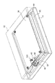
図1、図2、ならびに図3(a)および(b)を参照すると、上述した電子機器の一例は、積層配置された複数の電子モジュールとしてのLCDモジュール20、取付用板金50、および制御回路基板30と、取付用板金50の端部に形成された切欠部52を利用してLCDモジュール20に設けられたコネクタに積層方向に抜去可能に挿入されるコネクタ42と、制御回路基板30の板面に設けられたコネクタに積層方向に抜去可能に挿入されるコネクタ43と、液晶ディスプレイモジュール(LCD(Liquid Crystal Display)モジュール)20、取付用板金50、および制御回路基板30を収容するフロントケース11およびリアケース12から成る筐体とを有している。
Referring to FIGS. 1, 2, and 3 (a) and 3 (b), an example of the electronic device described above is an
コネクタ42とコネクタ43とはフラットケーブル41を介して接続されており、ケーブルコネクタ40として構成されている。よって、制御回路基板30とLCDモジュール20とは、ケーブルコネクタ40を介して、電気的に接続されている。
The
電子機器の正面に相当するフロントケース11の主面には、ウィンドゥ13が形成されており、LCDモジュール20の表示内容が視認可能になっている。
A
コネクタ42および43をも含め、コネクタは、一般に、電子機器の組み立て、修理、メインテナンスのために、抜去可能になっている。反面、電子機器を使用していく上で、電子機器に振動、衝撃等の外力が加わることは不可避であるため、不用意に抜けて、接触不良を起こす可能性がある。したがって、コネクタには、容易に抜けてしまわぬように、ロック手段が設けられる。
Connectors, including
しかし、コネクタ42および43は、電子機器の小型、軽量化や、低コスト化の目的から、電子モジュールに備えられている相手コネクタとの間で、いずれか一方が可撓性を有する凹部と凸部との組み合わせからなる簡易的なロック手段しか具備していない。このため、電子機器を使用していく上で、電子機器に振動、衝撃等の外力が加わった際に、コネクタ42および43が電子モジュールから抜け、接触不良を起こす虞がある。
However, for the purpose of reducing the size and weight of the electronic device and reducing the cost, one of the
図示した上述の電子機器においては、コネクタの抜けを防止するために、リアケース12の内側主面に、リブ122(ボスであってもよい)を備えている。これにより、リアケース12がフロントケース11に固定されると、リブ122がコネクタ43に当接する。よって、電子機器に振動、衝撃等の外力が加わったとしても、コネクタ43が制御回路基板30から抜けることがない。
In the illustrated electronic device, the rib 122 (which may be a boss) is provided on the inner main surface of the
尚、特許文献1には、スタッキングコネクタのロック機構が開示されている。 Patent Document 1 discloses a locking mechanism for a stacking connector.
しかし、コネクタ42に対しては、コネクタ43に対するリブ122のような策はとられていない。これは、リアケース12の内側主面から遠い位置にあるコネクタ42に到達するような高背のリブまたはボスを設けることが、設計上、製造上、および組み立て作業性の点から不利であるからである。このため、コネクタ42は、電子機器に振動、衝撃等の外力が加わった際にLCDモジュール20から抜ける虞がある。
However, no measures like the
尚、フラットケーブル40を長くしてコネクタ42をリアケース12の内側主面に近い所に配置し、コネクタ43に対するものと同様の策をとることも考えられるが、ノイズや信号ロス対策等の電気的な理由やコストの点から、ケーブルは可及的短い方が有利である。このため、コネクタ42の位置変更は、得策ではない。
Although the
それ故、本発明の課題は、積層された複数の電子モジュールに挿入される全てのコネクタについて抜けを確実に防止できるコネクタ用部品を提供することである。 SUMMARY OF THE INVENTION Therefore, an object of the present invention is to provide a connector component that can surely prevent disconnection of all connectors inserted into a plurality of stacked electronic modules.
本発明の他の課題は、そのようなコネクタ用部品を有するコネクタシステムを提供することである。 Another object of the present invention is to provide a connector system having such connector parts.
本発明のさらに他の課題は、そのようなコネクタシステムを有する電子機器を提供することである。 Still another object of the present invention is to provide an electronic apparatus having such a connector system.
本発明によれば、第1の電子モジュールと、該第1の電子モジュールに所定の間隔を置いて積層された第2の電子モジュールと、該第1の電子モジュールに積層方向に挿入される第1のコネクタと、該第2の電子モジュールに積層方向に挿入される第2のコネクタと、該第1および該第2の電子モジュールを収容する筐体とを有し、前記筐体は、前記第2の電子モジュールに対面する主面を有し、該主面には、前記第2のコネクタの抜けを規制する突出部が形成されている電子機器に適用されるコネクタ用部品であって、前記第1および前記第2のコネクタ間に配置され、該第2のコネクタに積層方向の動きを規制されることによって該第1のコネクタの抜けを規制することを特徴とするコネクタ用部品が得られる。 According to the present invention, the first electronic module, the second electronic module stacked on the first electronic module at a predetermined interval, and the first electronic module inserted in the stacking direction in the first electronic module. 1 connector, a second connector that is inserted into the second electronic module in the stacking direction, and a housing that accommodates the first and second electronic modules, A connector part that is applied to an electronic device having a main surface facing the second electronic module, the main surface having a protrusion that restricts the second connector from coming off; A connector component is provided which is disposed between the first and second connectors and restricts the first connector from coming off by restricting movement in the stacking direction by the second connector. It is done.
前記コネクタ用部品は、前記第1または前記第2のコネクタに装着されるものであってもよい。また、前記コネクタ用部品は、前記第1または前記第2のコネクタと一体に形成されているものであってもよい。 The connector component may be attached to the first or second connector. The connector component may be formed integrally with the first or second connector.
本発明によればまた、前記コネクタ用部品と、前記第1および前記第2のコネクタとを有するコネクタシステムが得られる。 According to the present invention, a connector system including the connector component and the first and second connectors can be obtained.
前記第1のコネクタと前記第2のコネクタとは、電気的に接続されていてもよい。また、前記第1のコネクタと前記第2のコネクタとは、互いに同じ形状を呈していてもよい。 The first connector and the second connector may be electrically connected. Further, the first connector and the second connector may have the same shape.
本発明によればさらに、前記コネクタシステムと、前記第1および前記第2の電子モジュールと、前記筐体とを有する電子機器が得られる。 According to the present invention, there is further obtained an electronic apparatus having the connector system, the first and second electronic modules, and the housing.
本発明によるコネクタ用部品は、積層された略板状を呈する複数の電子モジュールに挿入される全てのコネクタについて抜けを確実に防止できる。 The connector component according to the present invention can reliably prevent all connectors inserted into a plurality of stacked electronic modules having a substantially plate shape from being detached.
以下、本発明によるコネクタ用部品、コネクタシステム、および電子機器の実施形態について、図面を参照して詳細に説明する。 Hereinafter, embodiments of a connector part, a connector system, and an electronic device according to the present invention will be described in detail with reference to the drawings.
図4(a)および(b)、図5(a)および(b)、ならびに図6(a)〜(c)を参照すると、本実施形態によるコネクタ用部品であるインターポーザ60は、電子モジュールとしてのLCDモジュール20と、LCDモジュール20に取付用板金50を介して積層された電子モジュールとしての制御回路基板30と、LCDモジュール20に積層方向に抜去可能に挿入されるコネクタ42と、御回路基板30に積層方向に抜去可能に挿入されるコネクタ43と、LCDモジュール20を収容する筐体とを有する電子機器に適用されるコネクタ用部品である。この電子機器は、具体的には、例えば、POS(Point Of Sales)端末や多機能電話機に用いられる小型のディスプレイ装置である。
Referring to FIGS. 4A and 4B, FIGS. 5A and 5B, and FIGS. 6A to 6C, an
コネクタ42とコネクタ43とはフラットケーブル41を介して接続されており、ケーブルコネクタ40として構成されている。よって、制御回路基板30とLCDモジュール20とは、ケーブルコネクタ40を介して、電気的に接続されている。尚、コネクタ42とコネクタ43とは、互いに同じ形状を呈している。
The
上記筐体は、フロントケース11およびリアケース12から成っている。フロントケース11の主面には、ウィンドゥ13が形成されており、LCDモジュール20の表示内容が視認可能になっている。
The housing includes a
リアケース12は、御回路基板30に対面する主面を有している。この主面には、コネクタ43の抜けを規制する突出部としてのリブ(ボスであってもよい)122が形成されている。
The
以上のように、本発明によるインターポーザ60が適用される電子機器は、図1、図2、ならびに図3(a)および(b)に示された従来の電子機器と同様のものである。
As described above, the electronic device to which the
さて、インターポーザ60は、コネクタ42とコネクタ43との間に配置され、リブ122によって抜けが規制されたコネクタ43により電子モジュールの積層方向の動きを規制されることによってコネクタ42の抜けを規制するものである。即ち、本電子機器が組み立てられることにより、コネクタ43がリアケース12のリブ122によって抜けが規制されるが、これと同時に、コネクタ42の抜けも規制される。
The
インターポーザ60は、コネクタ43に容易には外れないように装着されている。これにより、本電子機器の組み立て途中に、インターポーザ60が配置されるべき所定の位置からズレたり、落下してしまうことがない。尚、インターポーザ60は、コネクタ42に装着されるか、あるいは、コネクタ42またはコネクタ43と一体に形成されているものであってもよい。
The
ケーブルコネクタ40と、インターポーザ60との組み合わせは、電子機器の筐体による抜けの規制の助けを得て、コネクタ42および43全ての抜けを防止する機能を有するコネクタシステムといえる。
The combination of the
以上説明した本電子機器の組み立て手順は、おおよそ次の通りである。 The procedure for assembling the electronic device described above is roughly as follows.
まず、作業台上に、フロントケース11をそのウィンドゥ13を下にして載置する。
First, the
次に、フロントケース11内に、LCDモジュール20を載置し、ネジ等によって固定する。
Next, the
LCDモジュール20上に、取付用板金50を、スペーサ55を介して載置し、ネジ等によって固定する。
A
さらに、取付用板金50上に、スペーサ55を介して制御回路基板30を、載置し、ネジ等によって固定する。尚、制御回路基板30を取付用板金50上にスペーサ55を介して固定してなるアセンブリを、LCDモジュール20上にスペーサ55を介して載置および固定してもよい。
Further, the
別途用意したケーブルコネクタ40のコネクタ42を、取付用板金50の端部に形成された切欠部52を利用して、LCDモジュール20に設けられたコネクタに電子モジュールの積層方向に挿入する。続いて、ケーブルコネクタ40のコネクタ43を、制御回路基板30に設けられたコネクタに電子モジュールの積層方向に挿入する。ここで、コネクタ43には、前もってインターポーザ60が装着されている。したがって、コネクタ43の挿入によって、コネクタ42とコネクタ43との間にインターポーザ60が介在した状態となる。
A separately
最後に、フロントケース11上に、リアケース12を載置および固定する。
Finally, the
以上のようにして、電子機器が組み立てられる。 The electronic device is assembled as described above.
フロントケース11にリアケース12が固定されることにより、リアケース12に形成されたリブ122がコネクタ43に当接し、コネクタ43の抜けが規制される。これと同時に、インターポーザ60がコネクタ43によって積層方向の動きを規制されることにより、コネクタ42の抜けも規制される。
By fixing the
以上説明した実施例に限定されることなく、本発明は、当該特許請求の範囲に記載された技術範囲内であれば、種々の変形が可能であることは云うまでもない。 The present invention is not limited to the embodiments described above, and it goes without saying that various modifications are possible within the technical scope described in the claims.
11 フロントケース
12 リアケース
13 ウィンドゥ
122 リブ
20 LCDモジュール
30 制御回路基板
40 ケーブルコネクタ
41 フラットケーブル
42、43 コネクタ
50 取付用板金
60 インターポーザ
DESCRIPTION OF
Claims (7)
前記第1および前記第2のコネクタ間に配置され、該第2のコネクタに積層方向の動きを規制されることによって該第1のコネクタの抜けを規制することを特徴とするコネクタ用部品。 A first electronic module; a second electronic module stacked on the first electronic module at a predetermined interval; a first connector inserted into the first electronic module in a stacking direction; A second connector that is inserted into the second electronic module in the stacking direction; and a housing that accommodates the first and second electronic modules, the housing being attached to the second electronic module A connector part that is applied to an electronic device having a main surface facing the main surface, wherein the main surface is formed with a protrusion that restricts the second connector from coming off;
A connector part that is disposed between the first connector and the second connector, and that restricts movement of the first connector by the movement of the second connector in the stacking direction.
Priority Applications (1)
| Application Number | Priority Date | Filing Date | Title |
|---|---|---|---|
| JP2007119650A JP4385341B2 (en) | 2007-04-27 | 2007-04-27 | Connector parts, connector systems, and electronic devices |
Applications Claiming Priority (1)
| Application Number | Priority Date | Filing Date | Title |
|---|---|---|---|
| JP2007119650A JP4385341B2 (en) | 2007-04-27 | 2007-04-27 | Connector parts, connector systems, and electronic devices |
Publications (2)
| Publication Number | Publication Date |
|---|---|
| JP2008277141A JP2008277141A (en) | 2008-11-13 |
| JP4385341B2 true JP4385341B2 (en) | 2009-12-16 |
Family
ID=40054857
Family Applications (1)
| Application Number | Title | Priority Date | Filing Date |
|---|---|---|---|
| JP2007119650A Active JP4385341B2 (en) | 2007-04-27 | 2007-04-27 | Connector parts, connector systems, and electronic devices |
Country Status (1)
| Country | Link |
|---|---|
| JP (1) | JP4385341B2 (en) |
Families Citing this family (2)
| Publication number | Priority date | Publication date | Assignee | Title |
|---|---|---|---|---|
| US10050359B2 (en) | 2013-10-31 | 2018-08-14 | Seiko Epson Corporation | Robot |
| JP2015085451A (en) * | 2013-10-31 | 2015-05-07 | セイコーエプソン株式会社 | Robot |
-
2007
- 2007-04-27 JP JP2007119650A patent/JP4385341B2/en active Active
Also Published As
| Publication number | Publication date |
|---|---|
| JP2008277141A (en) | 2008-11-13 |
Similar Documents
| Publication | Publication Date | Title |
|---|---|---|
| JP5080336B2 (en) | Board mounting connector | |
| JP5289712B2 (en) | Shield cover mounting structure and display device | |
| US7309240B2 (en) | Apparatus and electronic apparatus | |
| JP4385341B2 (en) | Connector parts, connector systems, and electronic devices | |
| JP4712461B2 (en) | Display panel connection cable protection structure and vehicle instrument assembly method | |
| CN111526689B (en) | Electronic device | |
| JP5523484B2 (en) | Mobile device | |
| US8029314B2 (en) | Connector for mounting a flexible printed circuit board | |
| JP2010251644A (en) | Security device | |
| EP3285117B1 (en) | Circuit board assembly and terminal | |
| JP4600224B2 (en) | Electronic device and connector connection structure used therefor | |
| JP4923807B2 (en) | PCB mounting structure | |
| JP5347375B2 (en) | Flexible board and wiring cable holding structure | |
| JP2011119531A (en) | Electronic apparatus | |
| KR101282877B1 (en) | Mobile terminal | |
| JP2010219433A (en) | Electronic equipment | |
| JP4546879B2 (en) | Mobile terminal device with camera | |
| JP2008208852A (en) | Fitting member and assembly | |
| JP5045659B2 (en) | Instrument | |
| JP2008199229A (en) | Reinforcing structure for external connection connector, and electronic equipment equipped with the same | |
| JP2004266021A (en) | Electronic equipment apparatus | |
| JP2016021061A (en) | Frame, display device, and television receiver | |
| JP2007311521A (en) | Fixing structure for flexible cable | |
| JP5294153B2 (en) | Electronics | |
| JP2009177321A (en) | Mobile terminal unit |
Legal Events
| Date | Code | Title | Description |
|---|---|---|---|
| A977 | Report on retrieval |
Free format text: JAPANESE INTERMEDIATE CODE: A971007 Effective date: 20090527 |
|
| A131 | Notification of reasons for refusal |
Free format text: JAPANESE INTERMEDIATE CODE: A131 Effective date: 20090603 |
|
| A521 | Written amendment |
Free format text: JAPANESE INTERMEDIATE CODE: A523 Effective date: 20090728 |
|
| TRDD | Decision of grant or rejection written | ||
| A01 | Written decision to grant a patent or to grant a registration (utility model) |
Free format text: JAPANESE INTERMEDIATE CODE: A01 Effective date: 20090902 |
|
| A01 | Written decision to grant a patent or to grant a registration (utility model) |
Free format text: JAPANESE INTERMEDIATE CODE: A01 |
|
| A61 | First payment of annual fees (during grant procedure) |
Free format text: JAPANESE INTERMEDIATE CODE: A61 Effective date: 20090917 |
|
| R150 | Certificate of patent or registration of utility model |
Ref document number: 4385341 Country of ref document: JP Free format text: JAPANESE INTERMEDIATE CODE: R150 Free format text: JAPANESE INTERMEDIATE CODE: R150 |
|
| FPAY | Renewal fee payment (event date is renewal date of database) |
Free format text: PAYMENT UNTIL: 20121009 Year of fee payment: 3 |
|
| FPAY | Renewal fee payment (event date is renewal date of database) |
Free format text: PAYMENT UNTIL: 20131009 Year of fee payment: 4 |
|
| S533 | Written request for registration of change of name |
Free format text: JAPANESE INTERMEDIATE CODE: R313533 |
|
| R350 | Written notification of registration of transfer |
Free format text: JAPANESE INTERMEDIATE CODE: R350 |