JP4781377B2 - Scanning device - Google Patents
Scanning device Download PDFInfo
- Publication number
- JP4781377B2 JP4781377B2 JP2008065756A JP2008065756A JP4781377B2 JP 4781377 B2 JP4781377 B2 JP 4781377B2 JP 2008065756 A JP2008065756 A JP 2008065756A JP 2008065756 A JP2008065756 A JP 2008065756A JP 4781377 B2 JP4781377 B2 JP 4781377B2
- Authority
- JP
- Japan
- Prior art keywords
- light
- optical element
- document
- illuminator
- phosphor
- Prior art date
- Legal status (The legal status is an assumption and is not a legal conclusion. Google has not performed a legal analysis and makes no representation as to the accuracy of the status listed.)
- Expired - Fee Related
Links
Images


Classifications
-
- H—ELECTRICITY
- H04—ELECTRIC COMMUNICATION TECHNIQUE
- H04N—PICTORIAL COMMUNICATION, e.g. TELEVISION
- H04N1/00—Scanning, transmission or reproduction of documents or the like, e.g. facsimile transmission; Details thereof
- H04N1/024—Details of scanning heads ; Means for illuminating the original
- H04N1/028—Details of scanning heads ; Means for illuminating the original for picture information pick-up
- H04N1/02815—Means for illuminating the original, not specific to a particular type of pick-up head
-
- H—ELECTRICITY
- H04—ELECTRIC COMMUNICATION TECHNIQUE
- H04N—PICTORIAL COMMUNICATION, e.g. TELEVISION
- H04N1/00—Scanning, transmission or reproduction of documents or the like, e.g. facsimile transmission; Details thereof
- H04N1/04—Scanning arrangements, i.e. arrangements for the displacement of active reading or reproducing elements relative to the original or reproducing medium, or vice versa
-
- H—ELECTRICITY
- H04—ELECTRIC COMMUNICATION TECHNIQUE
- H04N—PICTORIAL COMMUNICATION, e.g. TELEVISION
- H04N1/00—Scanning, transmission or reproduction of documents or the like, e.g. facsimile transmission; Details thereof
- H04N1/024—Details of scanning heads ; Means for illuminating the original
- H04N1/028—Details of scanning heads ; Means for illuminating the original for picture information pick-up
- H04N1/02815—Means for illuminating the original, not specific to a particular type of pick-up head
- H04N1/0282—Using a single or a few point light sources, e.g. a laser diode
- H04N1/02825—Using a single or a few point light sources, e.g. a laser diode in combination with at least one reflector which is fixed in relation to the light source
-
- H—ELECTRICITY
- H04—ELECTRIC COMMUNICATION TECHNIQUE
- H04N—PICTORIAL COMMUNICATION, e.g. TELEVISION
- H04N1/00—Scanning, transmission or reproduction of documents or the like, e.g. facsimile transmission; Details thereof
- H04N1/024—Details of scanning heads ; Means for illuminating the original
- H04N1/028—Details of scanning heads ; Means for illuminating the original for picture information pick-up
- H04N1/02815—Means for illuminating the original, not specific to a particular type of pick-up head
- H04N1/0282—Using a single or a few point light sources, e.g. a laser diode
- H04N1/02835—Using a single or a few point light sources, e.g. a laser diode in combination with a light guide, e.g. optical fibre, glass plate
-
- H—ELECTRICITY
- H04—ELECTRIC COMMUNICATION TECHNIQUE
- H04N—PICTORIAL COMMUNICATION, e.g. TELEVISION
- H04N1/00—Scanning, transmission or reproduction of documents or the like, e.g. facsimile transmission; Details thereof
- H04N1/024—Details of scanning heads ; Means for illuminating the original
- H04N1/028—Details of scanning heads ; Means for illuminating the original for picture information pick-up
- H04N1/02815—Means for illuminating the original, not specific to a particular type of pick-up head
- H04N1/02885—Means for compensating spatially uneven illumination, e.g. an aperture arrangement
- H04N1/0289—Light diffusing elements, e.g. plates or filters
-
- H—ELECTRICITY
- H04—ELECTRIC COMMUNICATION TECHNIQUE
- H04N—PICTORIAL COMMUNICATION, e.g. TELEVISION
- H04N1/00—Scanning, transmission or reproduction of documents or the like, e.g. facsimile transmission; Details thereof
- H04N1/024—Details of scanning heads ; Means for illuminating the original
- H04N1/028—Details of scanning heads ; Means for illuminating the original for picture information pick-up
- H04N1/02815—Means for illuminating the original, not specific to a particular type of pick-up head
- H04N1/02895—Additional elements in the illumination means or cooperating with the illumination means, e.g. filters
-
- H—ELECTRICITY
- H04—ELECTRIC COMMUNICATION TECHNIQUE
- H04N—PICTORIAL COMMUNICATION, e.g. TELEVISION
- H04N1/00—Scanning, transmission or reproduction of documents or the like, e.g. facsimile transmission; Details thereof
- H04N1/024—Details of scanning heads ; Means for illuminating the original
- H04N1/028—Details of scanning heads ; Means for illuminating the original for picture information pick-up
- H04N1/03—Details of scanning heads ; Means for illuminating the original for picture information pick-up with photodetectors arranged in a substantially linear array
- H04N1/031—Details of scanning heads ; Means for illuminating the original for picture information pick-up with photodetectors arranged in a substantially linear array the photodetectors having a one-to-one and optically positive correspondence with the scanned picture elements, e.g. linear contact sensors
- H04N1/0318—Integral pick-up heads, i.e. self-contained heads whose basic elements are a light-source, a lens array and a photodetector array which are supported by a single-piece frame
-
- H—ELECTRICITY
- H04—ELECTRIC COMMUNICATION TECHNIQUE
- H04N—PICTORIAL COMMUNICATION, e.g. TELEVISION
- H04N2201/00—Indexing scheme relating to scanning, transmission or reproduction of documents or the like, and to details thereof
- H04N2201/0077—Types of the still picture apparatus
- H04N2201/0081—Image reader
Description
本開示は、ディジタルスキャナー、ファクシミリ装置、およびディジタル複写機などにおけるディジタル記録のためにハードコピー原稿を照明するのに使用される照明装置に関する。具体的には、本開示は、光源とハードコピー原稿との間に置かれ、より均等な照明をもたらす燐光体材料を含む照明器に関する。 The present disclosure relates to an illuminating device used to illuminate hard copy originals for digital recording in digital scanners, facsimile machines, digital copiers, and the like. In particular, the present disclosure relates to an illuminator that includes a phosphor material that is placed between a light source and a hardcopy original to provide more even illumination.
ディジタル複写機およびファクシミリ装置などの事務機器においては、オリジナルのハードコピー原稿は、一般に「スキャナー」と呼ぶことができるものを用いて、ディジタルデータとして記録される。代表的なスキャナーにおいては、原稿シートは、照明され、そして、原稿シートから反射された光は、CCD(電荷結合素子)またはCMOS(相補型金属酸化膜半導体)アレイ(接触画像センサー(CIS)とも呼ばれる)などの感光装置によって記録されて、ディジタル画像データに変換される。原稿シートの連続する細いストリップは、シートが原稿ハンドラーを通して移動するにつれて、あるいは、原稿シートが載置されているプラテンに対して感光装置が移動するにつれて、照明される。原稿画像のこれらの細いストリップは、次いで、ソフトウェアによって組み立てられて、オリジナルの原稿の完全な画像表現となる。 In office equipment such as a digital copying machine and a facsimile machine, an original hard copy original is recorded as digital data using what can generally be called a “scanner”. In a typical scanner, the original sheet is illuminated and the light reflected from the original sheet is either a CCD (charge coupled device) or CMOS (complementary metal oxide semiconductor) array (contact image sensor (CIS)). Is recorded by a photosensitive device such as a digital image data. A continuous thin strip of document sheet is illuminated as the sheet moves through the document handler or as the photosensitive device moves relative to the platen on which the document sheet is placed. These thin strips of the original image are then assembled by software to provide a complete image representation of the original original document.
原稿のスキャニングに使用されるCISスキャンバーは、発光ダイオード(LED)および冷陰極蛍光灯(CCFL)を含む各種の照明源を使用してきた。CCFL照明は、単色スキャニングに直接使用することができ、あるいは、CCFL白色照明は、ピクセル上にRGB(赤色、緑色、および青色)カラーフィルターを有するセンサーを用いて、カラー画像をスキャンするのに使用することができる。CCFL照明は、非常に均等である傾向が有り、白色光を提供するが、このようなランプは、一般に、高電圧を使用し、かつ、消費電力量が高い。LEDベースの照明器は、一般に、内部反射を利用する光伝達要素を用いて、LEDからの光を導き、要素の出射面から原稿に向けて実質的に平行な光線として現れるようにする。このタイプのスキャンバーは、単一のLEDを用いて単色スキャンを行なうか、あるいは、赤色、青色、および緑色のLEDのトリプレット(例えば、InGaAlP、InGaN、およびGaPに基づく)を用いてカラー画像を捕獲することが多い。カラースキャンの場合は、RGBのLEDは、一度に一つずつ、連続してオン状態になり、3個の別個の画像をそれぞれ各色で照明して捕獲し、これらからフルカラースキャン画像を組み立てる。照明器は、3個のLED(RGB)のそれぞれからの照明を、原稿のストリップにわたってできるだけ均等に伝播させるためのプリズムを備えている。 CIS scan bars used for document scanning have used a variety of illumination sources including light emitting diodes (LEDs) and cold cathode fluorescent lamps (CCFLs). CCFL illumination can be used directly for monochromatic scanning, or CCFL white illumination can be used to scan color images using sensors with RGB (red, green, and blue) color filters on the pixels. can do. CCFL lighting tends to be very uniform and provides white light, but such lamps typically use high voltages and consume high amounts of power. LED-based illuminators typically use a light-transmitting element that utilizes internal reflection to direct light from the LED so that it appears as a substantially parallel light beam from the exit surface of the element toward the document. This type of scan bar performs a single color scan using a single LED or a color image using a triplet of red, blue, and green LEDs (eg, based on InGaAlP, InGaN, and GaP). Often captured. In the case of color scanning, the RGB LEDs are turned on, one at a time, and three separate images are illuminated and captured with each color, and a full color scanned image is assembled from them. The illuminator comprises a prism for propagating the illumination from each of the three LEDs (RGB) as evenly as possible across the original strip.
スキャナー用の照明器を設計する場合には、特に、原稿の細いストリップに沿って、すなわち、主走査(fast scan)方向に、均等な照明を行なうという課題が出てくる。これらのLEDベースの照明器のうちのあるものは、目標物である原稿から最も遠い照明器プリズムの側に、レンチキュラーなノッチ付きの後面を用いており、これにより、照明器の長さに沿って移動する光線を捕らえ、これらの光線を、スキャンバーの最も長い軸にほぼ垂直な方向に反射する。反射された光線は、次いで、照明器プリズムを前面から出て、目標物の原稿面を照明する。他のスキャンバーは、後面上に白色ペイントパターンを用い、これにより、空気に曝露される光学面に比べて屈折率を修正して、同様の効果を達成している。ノッチまたはペイントパターンは、光パイププリズムの長さに沿って変化するパターンを有しており、それにより、プリズムの近端(LEDに最も近い)(プリズムの近端における照明は、そのままでは、最も明るくなる傾向が有る)における照明と、プリズムの遠端(LEDから最も遠い)における照明とをバランスさせている。例えば、ノッチ付きの設計では、ノッチは、遠端でより深く、かつ、より大きく、また、近端でより浅い。この設計では、照明が最も明るくなるであろう近端におけるより小さなノッチは、全照明のうちのより少ない部分を原稿の方向に向け直し、遠端におけるより大きなノッチは、全照明のうちのより多くの部分を捕らえて、LED光源からより遠い存在を補償するよう、意図されている。しかしながら、このようなLED照明器の光パイププリズムは、依然として、相当な照明の不均等性を呈する。具体的には、それらは、スキャンバーの長さに沿って、または、ある色を別の色と比較した場合、均等な照明を提供しない傾向が有る。プリズムの遠端からの二次反射および他の散乱光線は、正確に均等な照明を成し遂げるのを難しくする傾向が有る。さらに、この設計では、鏡面反射領域と拡散照明領域との間が不均等になる傾向が有る。この最後のタイプの不均等性は、特に解決が難しい。なぜなら、一方の領域において不均等性を減らすため加えるいかなる修正も、結果として、他方の領域において不均等性の増大となる傾向が有るからである。一般に、二つの領域に対して一度に別様に較正することは可能ではなく、原稿面によっては、鏡面照明面と拡散照明面との組合せである場合がある(例えば、キメの粗い光沢面の場合は、光沢面の一部分が鏡面領域で反射し、残りの部分は拡散領域で照明される)。 When designing an illuminator for a scanner, there arises a problem of performing uniform illumination particularly along a thin strip of a document, that is, in a main scan direction. Some of these LED-based illuminators use a lenticular notched rear surface on the side of the illuminator prism furthest from the target document, thereby allowing for a length along the length of the illuminator. Capturing the light rays that travel in the direction of the scan bar and reflecting them in a direction substantially perpendicular to the longest axis of the scan bar. The reflected light then exits the illuminator prism from the front to illuminate the original document surface. Other scan bars use a white paint pattern on the back surface, thereby modifying the refractive index relative to the optical surface exposed to air to achieve a similar effect. The notch or paint pattern has a pattern that varies along the length of the light pipe prism, so that the near end of the prism (closest to the LED) (the illumination at the near end of the prism is the most The illumination at the far end of the prism (farthest from the LED) is balanced. For example, in a notched design, the notch is deeper and larger at the far end and shallower at the near end. In this design, the smaller notch at the near end where the illumination will be brightest redirects a smaller portion of the total illumination towards the document, and the larger notch at the far end is more than the total illumination. It is intended to capture many parts and compensate for being farther from the LED light source. However, such LED illuminator light pipe prisms still exhibit significant illumination non-uniformities. Specifically, they tend not to provide uniform illumination along the length of the scan bar or when comparing one color to another. Secondary reflections and other scattered rays from the far end of the prism tend to make it difficult to achieve exactly uniform illumination. Furthermore, this design tends to be uneven between the specular reflection area and the diffuse illumination area. This last type of non-uniformity is particularly difficult to resolve. This is because any modification made to reduce non-uniformity in one region tends to result in increased non-uniformity in the other region. In general, it is not possible to calibrate the two areas differently at once, and depending on the original surface, it may be a combination of a specular illumination surface and a diffuse illumination surface (for example, a rough glossy surface). In this case, a part of the glossy surface is reflected by the specular region and the remaining part is illuminated by the diffusion region).
照明される領域の照明レベルのばらつきは、画像データの欠陥となる場合があり、特にLEDなどの離散的な光源の場合は、ソフトウェアで完全に修正できない場合がある。 Variations in the illumination level of the illuminated area may result in image data defects, especially for discrete light sources such as LEDs, which may not be completely corrected by software.
好適な実施形態の第一態様によれば、スキャニング装置が、スキャンすべき原稿の一部分を照明するための照明器を備えている。前記照明器は、少なくとも一つの光源、前記光源によって放出される光を向け直すよう配置された光学要素、および前記光学要素によって向け直された前記光の少なくとも一部分を遮断する(intercept)よう配設された燐光体材料を備えている。前記原稿の画像を記録するため、前記原稿から反射された光を受け取るよう、感光装置が配置されている。 According to a first aspect of the preferred embodiment, the scanning device comprises an illuminator for illuminating a portion of the document to be scanned. The illuminator is arranged to intercept at least one light source, an optical element arranged to redirect light emitted by the light source, and at least a portion of the light redirected by the optical element Provided with a phosphor material. In order to record an image of the original, a photosensitive device is arranged to receive light reflected from the original.
前記装置において、前記光学要素は、前記燐光体材料を備えることができる。 In the apparatus, the optical element may comprise the phosphor material.
前記光学要素は、光伝達材料から形成される基体部分および前記燐光体材料を含む層を備えることができる。前記基体部分は、前記光源からの光を前記原稿の方に向け直すための少なくとも一つの反射要素を備えることができる。前記少なくとも一つの反射要素は、前記光学要素の後面に複数のノッチ(notch)を有することができる。前記少なくとも一つの反射要素は、前記光学要素の後面に、複数の反射ペイントパッチを有することができる。前記基体部分は、前記光源および前記燐光体含有層の中間である(intermediate)ことができる。 The optical element can comprise a substrate portion formed from a light transmitting material and a layer comprising the phosphor material. The base portion may include at least one reflecting element for redirecting light from the light source toward the document. The at least one reflective element may have a plurality of notches on the rear surface of the optical element. The at least one reflective element may have a plurality of reflective paint patches on the rear surface of the optical element. The substrate portion can be intermediate between the light source and the phosphor-containing layer.
前記少なくとも一つの光源は、発光ダイオードを含むことができる。 The at least one light source may include a light emitting diode.
前記燐光体材料は、前記光源からの光を、異なる波長の光、または所望の波長の組合せの光に変換することができる。前記光学要素によって放出された前記光(前記燐光体材料によって変換された光および前記LEDからの変換されていない光を含む)は、白色光に近似することができる。 The phosphor material can convert light from the light source into light of a different wavelength or a combination of desired wavelengths. The light emitted by the optical element (including light converted by the phosphor material and unconverted light from the LED) can approximate white light.
前記光学要素は、入射面および出射面を画成することができ、前記出射面は、前記入射面に略垂直であり、かつ、前記光源は、前記入射面に隣接して配置されており、かつ、前記燐光体材料は、前記出射面に隣接して配設されている。 The optical element can define an entrance surface and an exit surface, the exit surface is substantially perpendicular to the entrance surface, and the light source is disposed adjacent to the entrance surface; And the said phosphor material is arrange | positioned adjacent to the said output surface.
前記装置は、さらに、前記原稿を支持するためのプラテンを備えることができ、前記プラテンは、一般に、前記光学要素の出射面に隣接して配設されている。 The apparatus can further include a platen for supporting the document, and the platen is generally disposed adjacent to the exit surface of the optical element.
前記光学要素および前記少なくとも一つの光源は、可動キャリッジで支持することができる。 The optical element and the at least one light source can be supported by a movable carriage.
前記燐光体材料は、前記光学要素の後面上に配設することができる。 The phosphor material may be disposed on the rear surface of the optical element.
別の態様によれば、照明器が、入射面および対向する後面と出射面を画成する光学要素を備えている。前記出射面は、前記入射面に略垂直である。前記後面は、前記入射面から受け取った光を前記前面の方に向け直すための複数の反射要素を有している。前記反射要素と前記前面との間には、粒子材料が配設されていて、それに入射する光を拡散させる。前記入射面に隣接して、少なくとも一つの光源が配置されている。 According to another aspect, the illuminator includes an optical element that defines an entrance surface and opposing back and exit surfaces. The exit surface is substantially perpendicular to the entrance surface. The rear surface has a plurality of reflective elements for redirecting light received from the entrance surface toward the front surface. A particulate material is disposed between the reflective element and the front surface to diffuse light incident thereon. At least one light source is disposed adjacent to the incident surface.
前記照明器では、前記粒子材料は、少なくとも一つの燐光体を含むことができる。 In the illuminator, the particulate material may include at least one phosphor.
スキャニング装置が、前記照明器を備えることができ、かつ、前記原稿の画像を記録するため、前記原稿から反射された光を受け取るよう配置された感光装置をさらに備えることができる。 A scanning device may comprise the illuminator and may further comprise a photosensitive device arranged to receive light reflected from the document for recording an image of the document.
前記スキャニング装置は、単色スキャニング装置とすることができる。 The scanning device may be a monochromatic scanning device.
別の態様によれば、原稿をスキャンする方法が、光源を起動して光を放出すること、前記原稿を照明する光学要素を通して前記光を伝達することであって、前記光学要素の層を通して前記光を伝達することを含み、前記層は粒子材料を含み、これにより、前記原稿の前記照明は前記粒子材料無しの場合よりもより均等である、前記伝達することとを含んでいる。 According to another aspect, a method of scanning a document includes activating a light source to emit light, transmitting the light through an optical element that illuminates the document, and through the layer of the optical element Transmitting light, wherein the layer includes particulate material, whereby the illumination of the document is more uniform than without the particulate material.
前記伝達することは、前記発光光の少なくとも一部分を、複数の反射要素で、前記層の方に向け直すことをさらに含むことができる。 The transmitting can further include redirecting at least a portion of the emitted light toward the layer with a plurality of reflective elements.
前記伝達することは、前記光の少なくとも一部分を、前記燐光体材料で、より長い波長の光に変換することをさらに含むことができる。 The transmitting can further include converting at least a portion of the light with the phosphor material to light of a longer wavelength.
好適な実施形態の態様は、照明器に関し、かつ、照明器を組み込んでいる原稿スキャニング装置または「スキャナー」に関する。好適な実施形態はまた、物理的な原稿をスキャンして、スキャンされた画像を生成する方法にも関する。スキャンすべき原稿は、画像またはスキャンすべき画像が配設されている用紙のシートまたは他の柔軟性ある基体を含むことができる。スキャナーは、独立したスキャナー、複写機、ファクシミリ装置、または多機能装置などの撮像装置の一部を形成することができ、それにおいて、スキャンされた画像は、用紙上にレンダリングされ、かつ/あるいはディジタル形態で記憶されて、例えば、ディジタル形態で、表示、処理、または伝送される。好適なスキャニング装置は、原稿スキャナー、多機能プリンタ、通貨スキャナー、IDバッジスキャナー等に用途を見出している。 An aspect of the preferred embodiment relates to an illuminator and to a document scanning device or “scanner” incorporating the illuminator. The preferred embodiment also relates to a method of scanning a physical document to generate a scanned image. The document to be scanned can include an image or a sheet of paper or other flexible substrate on which the image to be scanned is disposed. The scanner can form part of an imaging device such as an independent scanner, copier, facsimile machine, or multifunction device, in which the scanned image is rendered on paper and / or digitally Stored in form, for example, displayed, processed, or transmitted in digital form. Suitable scanning devices find use in document scanners, multifunction printers, currency scanners, ID badge scanners, and the like.
照明器から放出された光は、一般に、拡散成分と鏡面成分とを有している。鏡面成分は、一般に、面が比較的均等な場合、光が原稿に当たったのと同じ角度で、ハードコピー原稿から反射される。状況によっては、照明源からの光の一部は、鏡面的に反射して、撮像センサーに入り、その信号出力に追加されることができる。従来のスキャナーでは、センサーに達する鏡面的に反射された光の量は、主走査方向における拡散照明の量に対して、異なる場合がある。 The light emitted from the illuminator generally has a diffusing component and a specular component. The specular component is generally reflected from the hardcopy original at the same angle that the light hits the original when the surface is relatively uniform. In some situations, some of the light from the illumination source can be specularly reflected and enter the imaging sensor and added to its signal output. In conventional scanners, the amount of specularly reflected light reaching the sensor may be different with respect to the amount of diffuse illumination in the main scanning direction.
好適な実施形態の態様では、照明器に燐光体材料が組み込まれている。燐光体材料は、一つまたはそれ以上の発光ダイオードまたはレーザーダイオード(これらは共に、ここでLEDという)などの光源によって放出された光を拡散する。好適な照明器は、このように、主走査方向により均等な照明を有して画像品質を向上させることができる。具体的には、撮像センサーに達する全光のうち鏡面的に反射された光の量が減少し、センサーに達する拡散光の量が増大する。 In a preferred embodiment aspect, the illuminator incorporates a phosphor material. The phosphor material diffuses light emitted by a light source, such as one or more light emitting diodes or laser diodes (both referred to herein as LEDs). A suitable illuminator can thus have more uniform illumination in the main scanning direction to improve image quality. Specifically, the amount of specularly reflected light out of the total light reaching the imaging sensor decreases, and the amount of diffused light reaching the sensor increases.
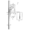
図1を参照すると、好適な実施形態による原稿スキャナーは、原稿シート12などのスキャン目標物を載置して、それから記録することができるプラテン10を備えている。オプションとしては、プラテン10に原稿ハンドラー(図示せず)を関連させて、それにより、複数ページのオリジナル原稿からシートを順次搬送する。
Referring to FIG. 1, a document scanner according to a preferred embodiment includes a
スキャンバー16が、原稿を照明するよう配置されており、照明器18および検出器20を備えている。検出器は、感光装置22およびレンズ構成24を備えている。照明器18は、原稿の細いストリップを照明し、一方、感光装置22(これは、一つまたはそれ以上の光センサーのリニアアレイを備えている)は、反射光を記録する。光センサーは、CCD(電荷結合素子)またはCMOS(相補型金属酸化膜半導体)デバイスなどのソリッドステートデバイスを含むことができる。検出器20は、適切な処理装置26を備えて、感光装置によって記録された反射光を表す信号を含む画像を生成する。プラテン10と感光装置22との間には、SEFLOC(登録商標)レンズまたは予め決められた受入角度を有する他のマイクロレンズ構成などのレンズ構成24が配置されて、光センサーアレイに反射光を集中させる。スキャンバー16は、可動キャリッジ28に取り付けられて、プラテン10の主要部分に載置されたシート上の画像から反射された光を記録することができる。一般に、キャリッジ28は、図1に示すように、方向Aに並進する。
A scan bar 16 is arranged to illuminate the document, and includes an
図2で最も良く分かるように、照明器18は、光学要素30を、光パイププリズム、および一つまたはそれ以上の発光ダイオードまたはレーザーダイオード(これらは、ここで共にLEDという)などの少なくとも一つの離散的な光源32(図示の実施形態では2個)の形態で備えている。光源32は、光を光学要素30内に向けるよう配置されている。ここで述べる好適な実施形態(二つまたはそれ以上の光源32が存在する)では、光源は同時に起動されるが、他の実施形態では、LEDは順次起動される場合があることが想定されている。光ファイバーの光ガイドなどの他の離散的な光源も想定されている。光学要素30は、ガラス、石英、ポリカーボネート、アクリル、または他のプラスチック材料などの任意の光学品質の光伝達材料で作ることができる。
As best seen in FIG. 2, the
図示の光学要素30は、光源32からの光を、プリズム内の内部反射の結果として、プラテンの撮像領域に向ける。図1および2では、光が移動する一般的な方向を示すため、光線は、概略的に示してある。一実施形態では、スキャナーは、二つの照明器18を備えており、これらは、照明すべき原稿の実質的に同じ小さな領域に光を向けるが、異なる方向から向ける。
The illustrated
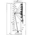
図2に示すように、光学要素30は、主走査方向、すなわち、スキャンバー16の移動の方向に垂直な方向にその最も長い寸法Lを有している。図2〜4の実施形態では、LEDの全ては、光学要素の最も長い寸法の一端面40に隣接して配設されている。小さな点様光源32が小さなLEDの形態で存在している場合は、各光源32は、入射面40におけるえくぼ形の凹所内に配設することができる。別法としてLEDは、どこか他所に配置して、端部から直角反射器で照明することができる。光学要素30は、後面44を備えており、これは、原稿12、および前面すなわち出射面46(それを通して光が原稿に向けられる面)から最も遠い面を構成している。後面および前面は、一般に、互いに他と平行に位置あわせすることができる。他の実施形態に示すように、前面は、後面に対して角度を付け、かつ/あるいは平面ではなく曲面にすることができる。
As shown in FIG. 2, the
複数の反射要素48が、後面44に沿って、配設されている。図示の反射要素48は、その間にノッチを画成している突起を有しているが、間隔を設けられた反射ペイントパッチ(paint patch)など、他の反射要素も設けることができることが想定されている。スキャンバー16におけるノッチ/ペイントパッチの数は、例えば、約20〜500とすることができる。LED32からの光線のうちのいくらかは、プリズム30の長さに沿って移動し、プリズムの後面44におけるノッチ48に当たる。ノッチは、光をスキャン目標物12に向けて反射する一連の小さなミラーとして動作する。したがって、LED32によって放出される光は、ノッチ48によって、光学要素の前面46に向けて反射される。突起/ノッチは、LED32の近くではより小さく、また、LEDから最も遠いプリズム30の端面49に向かって大きさが増大するものとして、図示してある。これは、光の分布をプリズムの長さLに亘って少なくとも部分的に等化するのに役立つ。別の実施形態では、ノッチは、長さLに沿って同じ大きさおよび形状のものとすることができる。
A plurality of
図1に示すように、発光光が、0度と90度との間の平均角度、例えば、約30〜60度で原稿に当たるよう、光学要素30は、原稿面に対して角度を付けることができる。図示の実施形態では、前面46は、原稿面の平面と略平行な平面内に存在しているが、別の実施形態では、前面46は、光線に対して、僅かに角度を付けることができる。面46における「傾斜」は、原稿の平面から5度と15度との間、例えば、約10度にすることができる。
As shown in FIG. 1, the
図2〜4に示すように、燐光体材料50は、LED32および原稿12の中間に配設されている。一実施形態では、燐光体材料は、光学要素の前面46を画成している層52内に組み込まれている。層52は、反射要素48を画成または支持している光学要素30の基体部分54と、プリズムの長さLに沿って、同一の空間に亘ることができる。一般に、層52および基体部分54は、例えば、基体部分54を燐光体含有材料で被覆またはオーバーモールドして、層52が、予め形成されている基体部分54に対する蓋体(cap)として役立つよう、層52を形成することによって、互いに他に固く付着されて、一つの統一体を形成している。層52は、基体部分54と同じ光学的に伝達可能な材料から形成することができるが、異なる材料が使用できることも想定されている。
As shown in FIGS. 2 to 4, the
図1に示すように、蓋体52および基体部分54は、それぞれ、光学要素の長さLに沿って、または少なくとも光学要素のページ幅全体に亘って、(例えば、ノッチ48の幅は別にして)実質的に同じ横断面輪郭を有することができる。
As shown in FIG. 1, the
図3〜5に示した実施形態では、光が主として後面44によって反射されてから燐光体材料50に当たるように、基体部分54は、光源(複数も可)32および燐光体含有層52の中間に配置されている。燐光体材料50は、層52全体に亘って比較的均質に分散されて、LEDから放出された光の少なくとも一部分を遮断する微粒子の形態とすることができる。燐光体材料は、それに衝突する光を拡散するのに役立ち、それにより、原稿に当たる光の不均等性を、燐光体材料無しで形成される同様のスキャンバーと比べて、減らすことになる。
In the embodiment shown in FIGS. 3-5, the
プリズム30は、少なくとも部分的にカバー56(例えば、キャリッジ)内に封じ込めることができる。図示の実施形態では、カバー56は、出射面46を除くプリズムの全ての面を取り囲んでいる。カバー56は、光が、プリズム内で内部的に反射されるよう、不透明な材料またはプリズムとは屈折率が異なる材料から作成することができる、。
The
図3は、LED光線60の、ノッチによる散乱で光線62が生じ、多数の方向に主として前面46に向かって移動する様、そして、光線62の、燐光体材料によるさらなる散乱で、光線64によって示すより散漫な光の散乱が生じる有様を示す。図4は、個々の燐光体粒子50が、光の拡散にいかに寄与するかを示す。燐光体粒子は、後面44に向かう方向を含む全ての方向に光を放出することができることが理解されるであろう。図1に示すように、この拡散発光の結果は、光のより大きい部分が、原稿12から拡散光(あらゆる角度で反射される光)(光線70によって示す)として反射され、かつ、光のより小さな部分が、鏡面光(スキャンバーのロッドレンズと平行であり、したがって、目標物からはね返され、光沢のある面からグレアを生じる傾向が有り、この光沢の有る面の下の画像をぼんやりさせる場合がある光の光線)(光線72によって示す)として反射される。
FIG. 3 shows that the LED light beam 60 is scattered by the notch to produce a
燐光体粒子50の放射特性は、プリズムの面仕上がり度の修正によって成し遂げられるよりも、より均等な光の拡散をもたらす傾向が有る。具体的には、燐光体粒子は、それらの隣の燐光体粒子にエネルギーを与える傾向が有り、このエネルギーの分配は、光線をより広く、かつ、より均等に伝播させることになる。なぜなら、光エネルギーは、より吸収的で、かつ、より損失がある面仕上がり度で予想されるよりも、より少ない照明の損失で、燐光体を通って伝播するからである。
The emission characteristics of the
一実施形態では、燐光体材料50は、LED32によって放出された光の少なくとも一部分を、異なる波長の光に変換するのに役立つ。例えば、LEDが、青色および/またはUV範囲などにおける比較的狭い波長の光を放出する場合は、燐光体材料は、発光光が可視範囲全体に亘って比較的均等に分散されるように、この光の少なくとも一部分を他の波長の光に変換することができる。このような比較的均等に分散される光は、「白色光」と呼ばれることが多い。「白色光」は、スペクトルが真に均等な分布から多少異なる、昼光、クール白色、ウォーム白色等、各種の微妙な明度を包含していることを理解されたい。これらの全ては、白色光に近い、と考えられる。何らかの用途に適した波長の他の組合せを、スキャンされる目標物のスペクトル構成により、選択することができる。波長領域におけるこの柔軟性の全ては、独自の発光特性を有する異なる燐光体の混合体から達成することができる。
In one embodiment, the
実際の一実施形態では、前面46の幅w(図1)は、約10〜15mmの範囲であり、面44と46との間の高さh(図3)は、約10〜20mmとすることができ、かつ、光学要素30の長さL(図2)は、スキャンすべき原稿の幅、例えば、約25〜30cmに近似させることができる。燐光体層52の厚さt(図3)は、約2mmまたはそれ以下、例えば、少なくとも1ミクロンとすることができる。
In one practical embodiment, the width w (FIG. 1) of the front face 46 is in the range of about 10-15 mm, and the height h (FIG. 3) between the
この技術で既知であるように、スキャナーは、スキャンされたディジタル画像を記憶させるためのメモリを備えることができる。スキャナーを組み込んでいるか、あるいは、それに結合されている画像レンダリング装置は、用紙などの基体上に、インクまたはトナーなどの色料を用いて、記憶された画像をレンダリングするマーキングエンジンなどの画像レンダリング構成要素を備えることができる。スキャナーを組み込んでいるか、あるいは、それに結合されているファクシミリ装置は、電話回線、ケーブルリンクまたは他の適切な有線または無線リンクを介して送信できる形態で記憶されたディジタル画像を出力する処理構成要素を備えることができる。 As is known in the art, the scanner can include a memory for storing the scanned digital image. An image rendering device that incorporates or is coupled to a scanner, such as a marking engine that renders a stored image on a substrate, such as paper, using a colorant, such as ink or toner, Elements can be provided. A facsimile machine incorporating or coupled to a scanner has a processing component that outputs a stored digital image in a form that can be transmitted over a telephone line, cable link, or other suitable wired or wireless link. Can be provided.
ここで開示されている好適な実施形態で使用するのに適した燐光体または燐光体の組合せで、LED32から白色光を生成するやり方には、各種のものがある。二つまたはそれ以上の燐光体を、燐光体材料50として使用する場合は、燐光体はブレンドの形態とすることができる。別法として、燐光体は、層52を共に構成する層の形態で、別個に配設することができる。
There are various ways of generating white light from the
一実施形態では、セリウムドープイットリウムアルミニウムガーネットY3Al5O2:Ce3+(「YAG:Ce」)またはセリウムドープテルビウムアルミニウムガーネットTb3Al5O12:Ce3+(「TAG:Ce」)などの単一の燐光体が使用される。青色光(InGaN LEDから放出されるものなど)は、燐光体を励起して、黄色光を放出させる。黄色光は、LEDによって放出される白色光に近い青色光と組み合せる。従来の燐光体表記では、コロンの前の成分がホストを表わし、一方、後の成分が賦活剤を表わす。 In one embodiment, cerium-doped yttrium aluminum garnet Y 3 Al 5 O 2 : Ce 3+ (“YAG: Ce”) or cerium-doped terbium aluminum garnet Tb 3 Al 5 O 12 : Ce 3+ (“TAG: Ce”) A single phosphor such as is used. Blue light (such as that emitted from an InGaN LED) excites the phosphor to emit yellow light. Yellow light is combined with blue light that is close to the white light emitted by the LED. In conventional phosphor notation, the component before the colon represents the host, while the component after the colon represents the activator.
別の実施形態では、燐光体材料は、二つの燐光体を含んでいる。例えば、第一の燐光体は、LEDからのUV/青色光を緑色光に変換し、一方、第二の燐光体は、UV/青色光を赤色光に変換する。このようなシステムは、例えば、特許文献1に開示されている。適切な緑色発光燐光体は、YBO3:Ce3+,Tb3+; BaMgAl10O17:Eu2+,Mn2+をY2O2S:Eu3+,Bi3+; YVO4:Eu3+,Bi3+; SrS:Eu2+; SrY2S4:Eu2+等の少なくとも一つの赤色発光燐光体との組合せで含んでいる。組合せ出力は、白色光に近い。 In another embodiment, the phosphor material includes two phosphors. For example, the first phosphor converts UV / blue light from the LED to green light, while the second phosphor converts UV / blue light to red light. Such a system is disclosed in Patent Document 1, for example. Suitable green emitting phosphors include YBO 3 : Ce 3+ , Tb 3+ ; BaMgAl 10 O 17 : Eu 2+ , Mn 2+ ; Y 2 O 2 S: Eu 3+ , Bi 3+ ; YVO 4 : Eu SrS: Eu 2+ ; SrY 2 S 4 : Eu 2+ and the like in combination with at least one red-emitting phosphor such as 3+ , Bi 3+ ; The combined output is close to white light.
他の実施形態では、第一の燐光体は、LED青色光を橙色光に変換し、一方、第二のそれは、青色光を黄緑色に変換する。組合せ出力は、白色光に近い。このような燐光体の組合せは、例えば、特許文献2に開示されている。別の二つの燐光体システムは、特許文献3に開示されている。このシステムでは、第一の燐光体は、橙色発光Eu2+,Mn2+ドープピロ燐酸ストロンチウム(Sr0.8Eu0.1Mn0.1)2P2O7とすることができ、第二の燐光体は、青緑色発光Eu2+ドープ(Sr0.90〜0.99Eu0.01〜0.1)4Al14O25とすることができる。
In other embodiments, the first phosphor converts LED blue light to orange light, while the second converts blue light to yellow-green. The combined output is close to white light. Such a combination of phosphors is disclosed in, for example,
別の実施形態では、燐光体は、赤色、緑色、および青色無機燐光体のそれぞれのうちの少なくとも一つなどの三つの(またはそれ以上の)燐光体を含んでいる。いずれの赤色、緑色、および青色無機燐光体も、ここで使用することができる。赤色燐光体は、(Sr,Ca,Ba,Mg)P2O7:Eu2+,Mn2+; CaLa2S4:Ce3+; SrY2S4:Eu2+; (Ca,Sr)S:Eu2+; SrS:Eu2+; Y2O3:Eu3+,Bi3+; YVO4:Eu3+,Bi3+; Y2O2S:Eu3+,Bi3+; Y2O2S:Eu3+からなるグループから選択された少なくとも一つの燐光体材料を含むことができる。緑色燐光体は、YBO3:Ce3,Tb3; BaMgAl10O17:Eu2+,Mn2+; (Sr,Ca,Ba)(Al,Ga)2S4:Eu2+; ZnS:Cu,Al; Ca8Mg(SiO4)4Cl2:Eu2+,Mn2+; Ba2SiO4:Eu2+; (Ba,Sr)2SiO4:Eu2+; Ba2(Mg,Zn)Si2O7:Eu2+; (Ba,Sr)Al2O4:Eu2+; およびSr2Si3O8.2SrCl2:Eu2+ からなるグループから選択された少なくとも一つの燐光体材料を含むことができる。青色燐光体は、(Sr,Mg,Ca)10(PO4)6Cl2:Eu2+; BaMgAl10O17:Eu2+; およびBaMg2Al16O27:Eu2+からなるグループから選択された少なくとも一つの燐光体材料を含むことができる。 In another embodiment, the phosphor includes three (or more) phosphors, such as at least one of each of red, green, and blue inorganic phosphors. Any red, green, and blue inorganic phosphor can be used here. The red phosphors are (Sr, Ca, Ba, Mg) P 2 O 7 : Eu 2+ , Mn 2+ ; CaLa 2 S 4 : Ce 3+ ; SrY 2 S 4 : Eu 2+ ; (Ca, Sr) S: Eu 2+; SrS: Eu 2+; Y 2 O 3: Eu 3+, Bi 3+; YVO 4: Eu 3+, Bi 3+; Y 2 O 2 S: Eu 3+, Bi 3+; At least one phosphor material selected from the group consisting of Y 2 O 2 S: Eu 3+ may be included. The green phosphor includes YBO 3 : Ce 3 , Tb 3 ; BaMgAl 10 O 17 : Eu 2+ , Mn 2+ ; (Sr, Ca, Ba) (Al, Ga) 2 S 4 : Eu 2+ ; ZnS: Cu , Al; Ca 8 Mg (SiO 4 ) 4 Cl 2 : Eu 2+ , Mn 2+ ; Ba 2 SiO 4 : Eu 2+ ; (Ba, Sr) 2 SiO 4 : Eu 2+ ; Ba 2 (Mg, Zn And (Ba, Sr) Al 2 O 4 : Eu 2+ ; and Sr 2 Si 3 O 8.2 SrCl 2 : Eu 2+ ; at least one phosphor material selected from the group consisting of: Si 2 O 7 : Eu 2+ ; Can be included. The blue phosphor is selected from the group consisting of (Sr, Mg, Ca) 10 (PO 4 ) 6 Cl 2 : Eu 2+ ; BaMgAl 10 O 17 : Eu 2+ ; and BaMg 2 Al 16 O 27 : Eu 2+ And at least one phosphor material formed.
白色光に近い光を作り出すための燐光体材料50として使用するのに適切な他の適切な燐光体粉の化学式が、特許文献4〜17に開示されている。さらに、好適な実施形態では、照明器18の出力は、近似する白色光の点から記述されているが、光は、白色光である必要はなく、いかなる適切な波長範囲のものであってもよいことを理解すべきである。
Other suitable phosphor powder chemical formulas suitable for use as the
一実施形態では、光源32からの光の波長は、360nm〜約490nmの範囲である。光源32は、約420〜470nmの範囲内に発光ピークを有していることができる。光源装置としては、窒化ガリウム(GaN)ベースの発光デバイスを使用することができる。ガリウムインジウム(GaIn)および窒化ガリウムインジウム(GaInN)ベースのLEDおよび他のLEDも想定されている。
In one embodiment, the wavelength of light from
単色(例えば、黒色および白色)スキャニングに適したスキャンバー16の場合は、照明器18は、単一のLEDまたは複数のLED32(これら全ては、狭い波長帯域で、例えば、青および(または)スペクトルのUV範囲で放出する)を、LEDからの光の少なくとも一部分を修正して、白色光に十分近いより広いスペクトルの光を発生させるための燐光体材料50との組合せで使用することができる。一態様では、照明器内の全ての光源は、同じタイプ、例えばUV/青色発光のものであり、したがって、同じ波長範囲で放出して、単色(例えば、青色)光を生じる。例えば、照明器内の全ての光源は、約470nm以下のピーク波長を有する光を放出する。燐光体材料は、発光光が、青色範囲(400〜490nm)内の光に加えて、490〜700nm(電磁スペクトルの緑〜赤色領域)の波長範囲内の光を含むように、発光光の一部分をより長い波長の光に変換する。
In the case of a scan bar 16 suitable for monochromatic (eg, black and white) scanning, the
用途のニーズにより(それが一般目的の原稿スキャニング、通貨スキャニング、または何らか他の目的であろうと)、燐光体製剤の発光光の色またはLEDの発光色は、スキャンされた画像で所望のレベルのコントラストを生じるある特定の色相を有するよう、選択することができる。例えば、センサー22が、ある特定の波長の光に、より受容性がある場合は、照明器18は、この波長に有利な光を発生するよう作成することができる。
Depending on the needs of the application (whether it is general purpose manuscript scanning, currency scanning, or some other purpose), the phosphor light emission color or LED light emission color is the desired level in the scanned image. Can be selected to have a certain hue that produces a contrast of. For example, if the
カラースキャニングでの使用に適したスキャンバー16の場合は、単色用途で説明したのと同様の照明器18を使用することができる。照明器18は、CCFL照明器を使用するスキャンバーで可能なやり方と同様のやり方で、各ピクセルで感知される色を制限するためのフィルタ付き画像センサー素子と共に使用することができる。例えば、フィルタは、順次適用して、赤色、緑色、および青色光が、順にセンサー22に到達することができるようにする。
In the case of a scan bar 16 suitable for use in color scanning, an
別法として、カラースキャニング用の照明器18は、電磁スペクトルの、それぞれ赤色、緑色、および青色領域を放出するなど、三つの異なる領域にピーク波長を有する3個のLEDを含むことができる。三つのLEDは、順次起動する。三つの波長に選択的に応答する燐光体材料は、順次赤色、緑色、および青色発光光を生じる。
Alternatively, the
好適な実施形態のいくつかの態様の利点は、拡散器として作用する燐光体層52による従来のCISシステムで得られる照明よりも均等な照明が得られる照明器18である。燐光体の各粒子50は、透明な光パイププリズム30によって分散されるLED32からの照明を集め、次いで、その光を多数の点光源から実質的に全方向的に再分散させることができる照明の点光源として作用することができる。これは、特に光沢のある原稿の場合、スキャンバー16にわたる光の均等性を増大させると共に、鏡面グレアの効果を低減する。
An advantage of some aspects of the preferred embodiment is an illuminator 18 that provides a more uniform illumination than that obtained with a conventional CIS system with a
好適な照明器は、このように、CCFLランプと同様の照明を行なうことができるが、LED32一個用の電力を必要とするだけである。より明るい照明のためには、追加のLEDまたはスーパーブライトLEDを使用することもできよう。好適な照明器18は、CCFLランプが有する非常に均等な、十分に分散され、かつ、十分に拡散された光の属性を有している。しかしながら、CCFL照明器に比べて、好適な照明器18は、一般に、より低いコストで製造することができ、脆弱性がより低く、かつ、破損を受けやすくなく、必要となる電力がはるかにより少なく、かつ、LED照明源32の電気的駆動条件を必要とするだけであろう。
A suitable illuminator can thus provide illumination similar to a CCFL lamp, but only requires power for one
好適な製造方法は、透明なアクリルまたは他の適切なポリマー材料から、射出成形によって、光パイププリズム30の基体部分54を製造することを含んでいる。基本的な照明器形状が成形されたら、次いで、同じ基材(透明なプラスチック基材に粉末状の白色燐光体充填剤を添加してある)から、前面(目標物原稿に対向する)をオーバーモールドする。LED(複数も可)32は、基体部分54内に画成されたえくぼ形の凹所に嵌め込むか、あるいは、スキャンバーの上部のチップに取り付けて、光を要素30に導入することができる。白色発光の燐光体充填剤50を有する前面層52は、光パイププリズムの透明な部分54を通して分散された光によってエネルギーを与えられると、主として、燐光体製剤によって放出される色であるが、LED32の色からの色も僅かに帯びた色にすることができる非常に散漫な光を放出する。
A preferred manufacturing method includes manufacturing the
図5は、特記する以外は、図1〜4の照明器と同様に構成することができる別の実施形態の照明器を示す。本実施形態では、燐光体材料50を含む層52は、プリズムの後面44に配設されている。燐光体は、ノッチ48それら自体によって成し遂げることができるよりも大きな程度まで光を拡散する。いくつかの実施形態では、ノッチ48は、省略することができる。本実施形態では、後面44は、粗面化することができる。
FIG. 5 shows another embodiment of an illuminator that can be configured similarly to the illuminator of FIGS. In this embodiment, the
Claims (2)
スキャンすべき原稿の一部分を照明するための照明器であって、
光学要素に光を向けるよう配置された少なくとも一つの光源と、
前記光源によって放出された光を向け直すよう配置された前記光学要素と、
前記光学要素によって向け直された光の少なくとも一部分を遮断するよう前記光源と前記原稿との間に配設された燐光体材料と、
を含む、前記照明器と、
前記原稿の画像を記録するため前記原稿から反射された光を受け取るよう配置された感光装置と、
を含み、
前記光学要素は、光透過材料からなる基部を含み、
前記光学要素は、入射面と、対向する後面及び出射面とを含み、該出射面は前記入射面に対して垂直であり、前記光源は前記入射面に隣接して配置され、
前記光学要素の後面は、前記入射面から前記基部に入射した光を前記出射面に向け直す複数のノッチ又はペイントパッチを含む複数の反射要素を含み、
前記出射面に隣接して前記燐光体材料を含む層が配置され、前記後面により向きなおされた光が前記層により拡散され前記出射面より出射する、
ことを特徴とするスキャニング装置。 A scanning device,
An illuminator for illuminating a portion of a document to be scanned,
At least one light source arranged to direct light to the optical element;
The optical element arranged to redirect the light emitted by the light source;
A phosphor material disposed between the light source and the original so as to block at least a portion of the light redirected by the optical element;
Including the illuminator,
A photosensitive device arranged to receive light reflected from the document for recording an image of the document;
Only including,
The optical element includes a base made of a light transmissive material;
The optical element includes an entrance surface, opposing rear and exit surfaces, the exit surface is perpendicular to the entrance surface, and the light source is disposed adjacent to the entrance surface;
The rear surface of the optical element includes a plurality of reflective elements including a plurality of notches or paint patches that redirect light incident on the base from the entrance surface to the exit surface;
A layer comprising the phosphor material is disposed adjacent to the exit surface, and the light redirected by the rear surface is diffused by the layer and exits from the exit surface;
A scanning device characterized by that.
スキャンすべき原稿の一部分を照明するための照明器であって、An illuminator for illuminating a portion of a document to be scanned,
光学要素に光を向けるよう配置された少なくとも一つの光源と、At least one light source arranged to direct light to the optical element;
前記光源によって放出された光を向け直すよう配置された前記光学要素と、The optical element arranged to redirect the light emitted by the light source;
前記光学要素によって向け直された光の少なくとも一部分を遮断するよう前記光源と前記原稿との間に配設された燐光体材料と、A phosphor material disposed between the light source and the original so as to block at least a portion of the light redirected by the optical element;
を含む、前記照明器と、Including the illuminator,
前記原稿の画像を記録するため前記原稿から反射された光を受け取るよう配置された感光装置と、A photosensitive device arranged to receive light reflected from the document for recording an image of the document;
を含み、Including
前記光学要素は、光透過材料からなる基部を含み、The optical element includes a base made of a light transmissive material;
前記光学要素は、入射面と、対向する後面及び出射面とを含み、該出射面は前記入射面に対して垂直であり、前記光源は前記入射面に隣接して配置され、The optical element includes an entrance surface, opposing rear and exit surfaces, the exit surface is perpendicular to the entrance surface, and the light source is disposed adjacent to the entrance surface;
前記光学要素の後面は、前記入射面から入射した光を拡散して前記出射面に向け直す前記燐光体材料を含む複数のノッチを含み、The rear surface of the optical element includes a plurality of notches including the phosphor material that diffuses and redirects light incident from the incident surface to the exit surface;
前記後面により向きなおされた光が前記出射面より出射する、The light redirected by the rear surface exits from the exit surface;
ことを特徴とするスキャニング装置。A scanning device characterized by that.
Applications Claiming Priority (2)
| Application Number | Priority Date | Filing Date | Title |
|---|---|---|---|
| US11/725,860 | 2007-03-20 | ||
| US11/725,860 US7864381B2 (en) | 2007-03-20 | 2007-03-20 | Document illuminator with LED-driven phosphor |
Publications (3)
| Publication Number | Publication Date |
|---|---|
| JP2008236747A JP2008236747A (en) | 2008-10-02 |
| JP2008236747A5 JP2008236747A5 (en) | 2011-03-03 |
| JP4781377B2 true JP4781377B2 (en) | 2011-09-28 |
Family
ID=39591969
Family Applications (1)
| Application Number | Title | Priority Date | Filing Date |
|---|---|---|---|
| JP2008065756A Expired - Fee Related JP4781377B2 (en) | 2007-03-20 | 2008-03-14 | Scanning device |
Country Status (5)
| Country | Link |
|---|---|
| US (1) | US7864381B2 (en) |
| EP (1) | EP1973325B1 (en) |
| JP (1) | JP4781377B2 (en) |
| KR (1) | KR20080085761A (en) |
| CN (1) | CN101272438A (en) |
Families Citing this family (19)
| Publication number | Priority date | Publication date | Assignee | Title |
|---|---|---|---|---|
| KR101279034B1 (en) * | 2007-07-11 | 2013-07-02 | 삼성전자주식회사 | Scanner module and image scanning apparatus |
| WO2009138255A1 (en) * | 2008-02-06 | 2009-11-19 | Contex A/S | Measuring and compensating for light intensity in an optical scanner |
| US8780206B2 (en) * | 2008-11-25 | 2014-07-15 | De La Rue North America Inc. | Sequenced illumination |
| US8265346B2 (en) | 2008-11-25 | 2012-09-11 | De La Rue North America Inc. | Determining document fitness using sequenced illumination |
| JP5336880B2 (en) | 2009-02-24 | 2013-11-06 | 日東光学株式会社 | Light emitting device |
| JP2010204539A (en) * | 2009-03-05 | 2010-09-16 | Ricoh Co Ltd | Original lighting device, image reading apparatus and image forming apparatus |
| US8094323B2 (en) * | 2009-06-26 | 2012-01-10 | Mitutoyo Corporation | Displacement encoder including phosphor illumination source |
| US8749767B2 (en) | 2009-09-02 | 2014-06-10 | De La Rue North America Inc. | Systems and methods for detecting tape on a document |
| US8433124B2 (en) * | 2010-01-07 | 2013-04-30 | De La Rue North America Inc. | Systems and methods for detecting an optically variable material |
| US8509492B2 (en) * | 2010-01-07 | 2013-08-13 | De La Rue North America Inc. | Detection of color shifting elements using sequenced illumination |
| US20110176181A1 (en) * | 2010-01-18 | 2011-07-21 | Mark Walter Fagan | Multi-Item Scanning on a Vertically Oriented Scanner |
| US9228701B2 (en) * | 2011-04-18 | 2016-01-05 | Marimils Oy | Illuminated stripe and illuminated stripe system |
| JP5903950B2 (en) * | 2012-03-14 | 2016-04-13 | 三菱電機株式会社 | Line light source for image reading |
| US9053596B2 (en) | 2012-07-31 | 2015-06-09 | De La Rue North America Inc. | Systems and methods for spectral authentication of a feature of a document |
| JP5841587B2 (en) * | 2013-12-25 | 2016-01-13 | 株式会社Pfu | Imaging system |
| KR20180000174A (en) * | 2016-06-22 | 2018-01-02 | 엘지이노텍 주식회사 | Phosphor plate and lighting device including the same |
| EP3551986A4 (en) | 2016-12-09 | 2020-08-05 | FormFactor, Inc. | Led light source probe card technology for testing cmos image scan devices |
| US11119263B2 (en) * | 2017-06-22 | 2021-09-14 | Xerox Corporation | System and method for image specific illumination of image printed on optical waveguide |
| CN112042613A (en) * | 2020-09-11 | 2020-12-08 | 杭州汉徽光电科技有限公司 | Method for pest control by blue light and converted light thereof |
Family Cites Families (42)
| Publication number | Priority date | Publication date | Assignee | Title |
|---|---|---|---|---|
| JP3116727B2 (en) | 1994-06-17 | 2000-12-11 | 日亜化学工業株式会社 | Planar light source |
| US6236470B1 (en) * | 1994-12-19 | 2001-05-22 | Xerox Corporation | Reflector and light source registration device for a document illuminator |
| US6316266B1 (en) * | 1995-06-07 | 2001-11-13 | Arizona State University Board Of Regents | Sample presentation apparatus for mass spectrometry |
| JP3133242B2 (en) * | 1995-12-08 | 2001-02-05 | スタンレー電気株式会社 | LED line light source device |
| JPH1097200A (en) | 1997-05-20 | 1998-04-14 | Nichia Chem Ind Ltd | Light source |
| US5813753A (en) * | 1997-05-27 | 1998-09-29 | Philips Electronics North America Corporation | UV/blue led-phosphor device with efficient conversion of UV/blues light to visible light |
| US6294800B1 (en) * | 1998-02-06 | 2001-09-25 | General Electric Company | Phosphors for white light generation from UV emitting diodes |
| US6252254B1 (en) * | 1998-02-06 | 2001-06-26 | General Electric Company | Light emitting device with phosphor composition |
| JPH11317108A (en) * | 1998-05-02 | 1999-11-16 | Canon Inc | Lighting apparatus, and image reading apparatus and image forming apparatus using the lighting apparatus |
| US6469808B1 (en) * | 1998-05-15 | 2002-10-22 | Rohm Co., Ltd. | Image reading apparatus and illuminator used for the same |
| EP1624667A2 (en) * | 1998-12-24 | 2006-02-08 | Canon Kabushiki Kaisha | Illumination apparatus using light guide |
| JP2000285718A (en) * | 1999-03-29 | 2000-10-13 | Rohm Co Ltd | Surface light source |
| US6354278B1 (en) * | 1999-03-30 | 2002-03-12 | Suzuki Kabushiki Kaisha | Engine of outboard motor |
| JP2001005122A (en) * | 1999-06-18 | 2001-01-12 | Canon Inc | Illumination device and image sensor, original reading device and information processing system having the same |
| JP2001061040A (en) * | 1999-08-20 | 2001-03-06 | Fujitsu Ltd | Illuminator |
| TW460716B (en) * | 1999-12-17 | 2001-10-21 | Toshiba Corp | Light guide, line illumination apparatus, and image acquisition system |
| US6522065B1 (en) * | 2000-03-27 | 2003-02-18 | General Electric Company | Single phosphor for creating white light with high luminosity and high CRI in a UV led device |
| US6501100B1 (en) * | 2000-05-15 | 2002-12-31 | General Electric Company | White light emitting phosphor blend for LED devices |
| US6621211B1 (en) * | 2000-05-15 | 2003-09-16 | General Electric Company | White light emitting phosphor blends for LED devices |
| US6635987B1 (en) * | 2000-09-26 | 2003-10-21 | General Electric Company | High power white LED lamp structure using unique phosphor application for LED lighting products |
| JP3392117B2 (en) * | 2000-12-01 | 2003-03-31 | キヤノン株式会社 | Light guide for reader and reader |
| AT410266B (en) * | 2000-12-28 | 2003-03-25 | Tridonic Optoelectronics Gmbh | LIGHT SOURCE WITH A LIGHT-EMITTING ELEMENT |
| US6685852B2 (en) * | 2001-04-27 | 2004-02-03 | General Electric Company | Phosphor blends for generating white light from near-UV/blue light-emitting devices |
| TWI221385B (en) * | 2001-05-31 | 2004-09-21 | Mustek Systems Inc | CCD type scanner powered by a serial bus |
| JP4672918B2 (en) * | 2001-07-12 | 2011-04-20 | キヤノン株式会社 | Image sensor and image reading apparatus |
| US6809471B2 (en) * | 2002-06-28 | 2004-10-26 | General Electric Company | Phosphors containing oxides of alkaline-earth and Group-IIIB metals and light sources incorporating the same |
| US20040057082A1 (en) * | 2002-09-24 | 2004-03-25 | Rong-Ji Liu | Method of focusing a selected scanning area for document scanning device |
| JP4087681B2 (en) * | 2002-10-29 | 2008-05-21 | 株式会社日立製作所 | LIGHTING DEVICE AND DISPLAY DEVICE USING THE SAME |
| US6936857B2 (en) * | 2003-02-18 | 2005-08-30 | Gelcore, Llc | White light LED device |
| US7400429B2 (en) * | 2003-03-17 | 2008-07-15 | Kabushiki Kaisha Toshiba | Image reading apparatus |
| US7038370B2 (en) * | 2003-03-17 | 2006-05-02 | Lumileds Lighting, U.S., Llc | Phosphor converted light emitting device |
| US7157745B2 (en) * | 2004-04-09 | 2007-01-02 | Blonder Greg E | Illumination devices comprising white light emitting diodes and diode arrays and method and apparatus for making them |
| US7529445B2 (en) * | 2003-06-25 | 2009-05-05 | Nippon Sheet Glass Co., Ltd | Light guide and line illuminator |
| US7075225B2 (en) * | 2003-06-27 | 2006-07-11 | Tajul Arosh Baroky | White light emitting device |
| US7112921B2 (en) * | 2003-08-02 | 2006-09-26 | Phosphortech Inc. | Light emitting device having selenium-based fluorescent phosphor |
| JP4638192B2 (en) | 2004-08-26 | 2011-02-23 | 三菱電機株式会社 | Line light source and contact image sensor using the same |
| US7746520B2 (en) * | 2004-11-23 | 2010-06-29 | Xerox Corporation | Document illuminator |
| US7715063B2 (en) * | 2005-03-31 | 2010-05-11 | Xerox Corporation | CVT integrated illuminator |
| US7593143B2 (en) * | 2005-03-31 | 2009-09-22 | Xerox Corporation | Compound curved concentrator based illuminator |
| CN100403563C (en) * | 2005-04-18 | 2008-07-16 | 光宝科技股份有限公司 | LED with white light and fluorescent powder concerned and preparation thereof |
| US7755811B2 (en) * | 2005-06-30 | 2010-07-13 | Xerox Corporation | Document illuminator |
| JP2008219405A (en) * | 2007-03-02 | 2008-09-18 | Ushio Inc | Linear light source device |
-
2007
- 2007-03-20 US US11/725,860 patent/US7864381B2/en not_active Expired - Fee Related
-
2008
- 2008-02-25 EP EP08151898.7A patent/EP1973325B1/en not_active Expired - Fee Related
- 2008-03-14 JP JP2008065756A patent/JP4781377B2/en not_active Expired - Fee Related
- 2008-03-19 KR KR1020080025363A patent/KR20080085761A/en not_active Application Discontinuation
- 2008-03-19 CN CNA2008100854800A patent/CN101272438A/en active Pending
Also Published As
| Publication number | Publication date |
|---|---|
| US20080231911A1 (en) | 2008-09-25 |
| US7864381B2 (en) | 2011-01-04 |
| EP1973325A1 (en) | 2008-09-24 |
| EP1973325B1 (en) | 2015-08-05 |
| CN101272438A (en) | 2008-09-24 |
| KR20080085761A (en) | 2008-09-24 |
| JP2008236747A (en) | 2008-10-02 |
Similar Documents
| Publication | Publication Date | Title |
|---|---|---|
| JP4781377B2 (en) | Scanning device | |
| US20060187500A1 (en) | Image reading device, image forming apparatus, and image reading method | |
| US8885231B2 (en) | Illumination apparatus, image sensor unit, image reading apparatus, and image forming apparatus | |
| JP2005198106A (en) | Line lighting system and image scanner | |
| JP2001343531A (en) | Illumination device, image sensor having this illumination device and image reader and information processing system using this image sensor | |
| JP2003046726A (en) | Device for reading print pattern of a variety of paper leaves | |
| JP2002185708A (en) | Illuminator, image sensor unit and image reader provided with the same | |
| JP4742153B2 (en) | Document reader | |
| US7760434B2 (en) | Document illuminator with surface lens | |
| JPH1184544A (en) | Line illuminator | |
| JP2010219714A (en) | Illumination device and image reading apparatus | |
| US9172836B2 (en) | Optical scanner illumination system and method | |
| JP6128897B2 (en) | Illumination device and image reading device | |
| JP2010068412A (en) | Lighting device and image reading unit using the same | |
| JP2000324308A (en) | Led linear light source | |
| US7057777B2 (en) | Optical image scanning device with fluorescent layer as back light | |
| JP2001111795A (en) | Image reader | |
| CN102238310A (en) | Image scanning device | |
| JP2004221729A (en) | Close contact type image sensor and close contact type image reader using the same | |
| US20050041269A1 (en) | Image forming apparatus and image scanning method | |
| JP2001045225A (en) | Image reader | |
| JP5059327B2 (en) | Illumination device for image reading apparatus | |
| JP2008116527A (en) | Light source unit, reader, image reader and image forming apparatus | |
| TWM358310U (en) | Light guiding system for contact image sensor | |
| JP6720022B2 (en) | Lighting device and image reading device |
Legal Events
| Date | Code | Title | Description |
|---|---|---|---|
| A521 | Written amendment |
Free format text: JAPANESE INTERMEDIATE CODE: A523 Effective date: 20110119 |
|
| A621 | Written request for application examination |
Free format text: JAPANESE INTERMEDIATE CODE: A621 Effective date: 20110119 |
|
| A871 | Explanation of circumstances concerning accelerated examination |
Free format text: JAPANESE INTERMEDIATE CODE: A871 Effective date: 20110119 |
|
| A975 | Report on accelerated examination |
Free format text: JAPANESE INTERMEDIATE CODE: A971005 Effective date: 20110208 |
|
| A131 | Notification of reasons for refusal |
Free format text: JAPANESE INTERMEDIATE CODE: A131 Effective date: 20110215 |
|
| A521 | Written amendment |
Free format text: JAPANESE INTERMEDIATE CODE: A523 Effective date: 20110512 |
|
| TRDD | Decision of grant or rejection written | ||
| A01 | Written decision to grant a patent or to grant a registration (utility model) |
Free format text: JAPANESE INTERMEDIATE CODE: A01 Effective date: 20110607 |
|
| A01 | Written decision to grant a patent or to grant a registration (utility model) |
Free format text: JAPANESE INTERMEDIATE CODE: A01 |
|
| A61 | First payment of annual fees (during grant procedure) |
Free format text: JAPANESE INTERMEDIATE CODE: A61 Effective date: 20110705 |
|
| FPAY | Renewal fee payment (event date is renewal date of database) |
Free format text: PAYMENT UNTIL: 20140715 Year of fee payment: 3 |
|
| R150 | Certificate of patent or registration of utility model |
Ref document number: 4781377 Country of ref document: JP Free format text: JAPANESE INTERMEDIATE CODE: R150 Free format text: JAPANESE INTERMEDIATE CODE: R150 |
|
| R250 | Receipt of annual fees |
Free format text: JAPANESE INTERMEDIATE CODE: R250 |
|
| R250 | Receipt of annual fees |
Free format text: JAPANESE INTERMEDIATE CODE: R250 |
|
| R250 | Receipt of annual fees |
Free format text: JAPANESE INTERMEDIATE CODE: R250 |
|
| R250 | Receipt of annual fees |
Free format text: JAPANESE INTERMEDIATE CODE: R250 |
|
| R250 | Receipt of annual fees |
Free format text: JAPANESE INTERMEDIATE CODE: R250 |
|
| LAPS | Cancellation because of no payment of annual fees |