EP1973325B1 - Document Illuminator with LED-Driven Phosphor - Google Patents
Document Illuminator with LED-Driven Phosphor Download PDFInfo
- Publication number
- EP1973325B1 EP1973325B1 EP08151898.7A EP08151898A EP1973325B1 EP 1973325 B1 EP1973325 B1 EP 1973325B1 EP 08151898 A EP08151898 A EP 08151898A EP 1973325 B1 EP1973325 B1 EP 1973325B1
- Authority
- EP
- European Patent Office
- Prior art keywords
- light
- optical element
- document
- face
- light source
- Prior art date
- Legal status (The legal status is an assumption and is not a legal conclusion. Google has not performed a legal analysis and makes no representation as to the accuracy of the status listed.)
- Expired - Fee Related
Links
Images

Classifications
-
- H—ELECTRICITY
- H04—ELECTRIC COMMUNICATION TECHNIQUE
- H04N—PICTORIAL COMMUNICATION, e.g. TELEVISION
- H04N1/00—Scanning, transmission or reproduction of documents or the like, e.g. facsimile transmission; Details thereof
- H04N1/024—Details of scanning heads ; Means for illuminating the original
- H04N1/028—Details of scanning heads ; Means for illuminating the original for picture information pick-up
- H04N1/02815—Means for illuminating the original, not specific to a particular type of pick-up head
-
- H—ELECTRICITY
- H04—ELECTRIC COMMUNICATION TECHNIQUE
- H04N—PICTORIAL COMMUNICATION, e.g. TELEVISION
- H04N1/00—Scanning, transmission or reproduction of documents or the like, e.g. facsimile transmission; Details thereof
- H04N1/04—Scanning arrangements, i.e. arrangements for the displacement of active reading or reproducing elements relative to the original or reproducing medium, or vice versa
-
- H—ELECTRICITY
- H04—ELECTRIC COMMUNICATION TECHNIQUE
- H04N—PICTORIAL COMMUNICATION, e.g. TELEVISION
- H04N1/00—Scanning, transmission or reproduction of documents or the like, e.g. facsimile transmission; Details thereof
- H04N1/024—Details of scanning heads ; Means for illuminating the original
- H04N1/028—Details of scanning heads ; Means for illuminating the original for picture information pick-up
- H04N1/02815—Means for illuminating the original, not specific to a particular type of pick-up head
- H04N1/0282—Using a single or a few point light sources, e.g. a laser diode
- H04N1/02825—Using a single or a few point light sources, e.g. a laser diode in combination with at least one reflector which is fixed in relation to the light source
-
- H—ELECTRICITY
- H04—ELECTRIC COMMUNICATION TECHNIQUE
- H04N—PICTORIAL COMMUNICATION, e.g. TELEVISION
- H04N1/00—Scanning, transmission or reproduction of documents or the like, e.g. facsimile transmission; Details thereof
- H04N1/024—Details of scanning heads ; Means for illuminating the original
- H04N1/028—Details of scanning heads ; Means for illuminating the original for picture information pick-up
- H04N1/02815—Means for illuminating the original, not specific to a particular type of pick-up head
- H04N1/0282—Using a single or a few point light sources, e.g. a laser diode
- H04N1/02835—Using a single or a few point light sources, e.g. a laser diode in combination with a light guide, e.g. optical fibre, glass plate
-
- H—ELECTRICITY
- H04—ELECTRIC COMMUNICATION TECHNIQUE
- H04N—PICTORIAL COMMUNICATION, e.g. TELEVISION
- H04N1/00—Scanning, transmission or reproduction of documents or the like, e.g. facsimile transmission; Details thereof
- H04N1/024—Details of scanning heads ; Means for illuminating the original
- H04N1/028—Details of scanning heads ; Means for illuminating the original for picture information pick-up
- H04N1/02815—Means for illuminating the original, not specific to a particular type of pick-up head
- H04N1/02885—Means for compensating spatially uneven illumination, e.g. an aperture arrangement
- H04N1/0289—Light diffusing elements, e.g. plates or filters
-
- H—ELECTRICITY
- H04—ELECTRIC COMMUNICATION TECHNIQUE
- H04N—PICTORIAL COMMUNICATION, e.g. TELEVISION
- H04N1/00—Scanning, transmission or reproduction of documents or the like, e.g. facsimile transmission; Details thereof
- H04N1/024—Details of scanning heads ; Means for illuminating the original
- H04N1/028—Details of scanning heads ; Means for illuminating the original for picture information pick-up
- H04N1/02815—Means for illuminating the original, not specific to a particular type of pick-up head
- H04N1/02895—Additional elements in the illumination means or cooperating with the illumination means, e.g. filters
-
- H—ELECTRICITY
- H04—ELECTRIC COMMUNICATION TECHNIQUE
- H04N—PICTORIAL COMMUNICATION, e.g. TELEVISION
- H04N1/00—Scanning, transmission or reproduction of documents or the like, e.g. facsimile transmission; Details thereof
- H04N1/024—Details of scanning heads ; Means for illuminating the original
- H04N1/028—Details of scanning heads ; Means for illuminating the original for picture information pick-up
- H04N1/03—Details of scanning heads ; Means for illuminating the original for picture information pick-up with photodetectors arranged in a substantially linear array
- H04N1/031—Details of scanning heads ; Means for illuminating the original for picture information pick-up with photodetectors arranged in a substantially linear array the photodetectors having a one-to-one and optically positive correspondence with the scanned picture elements, e.g. linear contact sensors
- H04N1/0318—Integral pick-up heads, i.e. self-contained heads whose basic elements are a light-source, a lens array and a photodetector array which are supported by a single-piece frame
-
- H—ELECTRICITY
- H04—ELECTRIC COMMUNICATION TECHNIQUE
- H04N—PICTORIAL COMMUNICATION, e.g. TELEVISION
- H04N2201/00—Indexing scheme relating to scanning, transmission or reproduction of documents or the like, and to details thereof
- H04N2201/0077—Types of the still picture apparatus
- H04N2201/0081—Image reader
Description
- The present disclosure relates to an illuminating apparatus used to illuminate hard-copy documents for digital recording, such as in digital scanners, facsimile machines, and digital copiers. In particular, it relates to an illuminator which includes a phosphor material interposed between a light source and the hard-copy document, which provides a more even illumination.
- In office equipment, such as digital copiers and facsimile machines, original hard-copy documents are recorded as digital data using what can be generally called a "scanner." In a typical scanner, a document sheet is illuminated and the light reflected from the document sheet is recorded by a photosensitive device such as a CCD (charge coupled device) or CMOS (complementary metal oxide semiconductor) array (also known as a contact image sensor (CIS)), to be converted to digital image data. Successive narrow strips of the document sheet are illuminated as the sheet is moved through a document handler, or the photosensitive device is moved relative to a platen on which the document sheet is placed. These narrow strips of document image are then assembled by software into a complete image representation of the original document.
- CIS scan bars used for document scanning have used a variety of illumination sources, including light emitting diodes (LEDs) and cold cathode fluorescent lamps (CCFL). CCFL illumination can be used directly for monochrome scanning, or by using sensors with an array of RGB (Red, Green, and Blue) color filters over the pixels, CCFL white illumination can be used to scan color images. While CCFL illumination tends to be very uniform and provides white light, such lamps generally employ high voltages and have a high power consumption. LED-based illuminators typically employ a light-transmissive element that exploits internal reflections to direct light from LEDs to emerge in substantially parallel rays from an exit surface of the element toward a document. Scan bars of this type often use a single LED for monochrome scans or a red, blue, and green triplet of LEDs (e.g., based on InGaAIP, InGaN, and GaP) to capture color images. For color scans, the RGB LEDs are turned on one at a time in succession, in order to capture three separate images, one illuminated with each color, from which a full color scan image is then assembled. The illuminator includes a prism for spreading the illumination from each of the three LEDs (RGB) across a strip of the document as uniformly as possible.
- Designing an illuminator for a scanner presents challenges in providing, among other aspects, an even illumination along the narrow strip of the document, i.e., in the fast scan direction. Some of these LED-based illuminators use a lenticular, notched rear surface, on the side of the illuminator prism furthest from the document target, which catches the light rays traveling down the length of the illuminator and reflects these rays in a direction which is approximately perpendicular to the longest axis of the scan bar. The reflected rays then exit the illuminator prism from a front surface and illuminate the target document surface. Other scan bars use a white paint pattern on the rear surface, which modifies the index of refraction, as compared to an optical surface exposed to air, to accomplish a similar effect. The notches or paint patterns have a pattern which varies down the length of the light pipe prism in an effort to balance the illumination at the near-end of the prism (closest to the LEDs), where the illumination would otherwise tend to be brightest, with the illumination at the far-end of the prism (farthest from the LEDs), For example, in the notched designs, the notches are deeper and larger at the far-end and shallower at the near-end. In this design, the smaller notches at the near-end where the illumination would be brightest redirect less of the total illumination in the direction of the document, and the larger notches at the far-end are intended to catch more of the total illumination to compensate for being farther from the LED source. However, such LED illuminator light-pipe prisms still exhibit significant illumination non-uniformity. Specifically, they tend not to provide uniform illumination down the length of the scan bar, or when comparing one color to another. Secondary reflections from the far-end of the prism and other scattered light rays tend to make precisely uniform illumination difficult to achieve. Additionally, this design tends to be non-uniform between the specular reflective, and diffuse illumination domains. This last type of non-uniformity is particularly problematic because any correction applied to reduce non-uniformity in one domain tends to result in an increase in non-uniformity in the other. It is generally not possible to calibrate differently for the two domains at one time, and some document surfaces are a combination of specular and diffuse illumination surfaces (e.g., a shiny pebble-grained surface where portions of the shiny surface reflect in the specular domain with the rest being illuminated in the diffuse domain.
- Irregularities in the illumination level in the illuminated area can result in defects in the image data, which may not be completely correctable in software, particularly in the case of discrete light sources, such as LEDs.
-
JP 2006067197 A -
US 2001/0019487 A1 describes light guide, line illumination apparatus, and image acquisition system. The invention concerns a line illumination apparatus and an image acquisition system, comprising a light guide including a transparent member in the shape of a bar, and a light source provided at the end of the light guide in the longitudinal direction relative to the light guide, wherein the light guide comprises a scattering mark configured to scatter a light transmitted inside the transparent member from the light source substantially vertical to the longitudinal direction relative to the transparent member, a reflection surface having a curved surface configured to reflect a light scattered at the scattering mark inside the transparent member, and a light exit surface configured to enable a light reflected at the reflection surface to exit outside the transparent member therethrough. -
JP 08007614 A -
JP 10097200 A - It is the object of the present invention to improve a scanning apparatus particularly with regard to improved document illumination. This object is achieved by providing a scanning apparatus according to claim 1 and a method for preparing a scanning apparatus according to claim 8. Embodiments of the invention are set forth in the dependent claims.
-
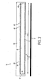
FIGURE 1 is a simplified elevational view of a document scanner according to the exemplary embodiment; -
FIGURE 2 is an enlarged schematic view of the illuminator ofFIGURE 1 ; -
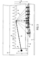
FIGURE 3 is an enlarged schematic view of a portion of the illuminator ofFIGURE 2 , illustrating directions of light rays in the prism; -
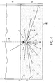
FIGURE 4 is an enlarged schematic view of a portion of the illuminator ofFIGURE 3 , illustrating directions of light rays sticking phosphor particles; and -
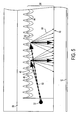
FIGURE 5 is an enlarged schematic view of another embodiment of a portion of an illuminator suited to use in the document scanner ofFIGURE 1 . - Aspects of the exemplary embodiment relate to an illuminator and to a document scanning apparatus or "scanner" which incorporates the illuminator. The exemplary embodiment also relates to a method of scanning physical documents for generating scanned images. The documents to be scanned may comprise sheets of paper or other flexible substrate, on which an image or images to be scanned is disposed. The scanner may form a part of an imaging device, such as such as a stand-alone scanner, a copier, a facsimile machine, or a multifunction device, in which a scanned image is rendered on paper and/or stored in digital form, for example, for display, processing, or transmission in digital form. The exemplary scanning device finds application in document scanners, multi-function printers, currency scanners, ID badge scanners, and the like.
- Light emitted from an illuminator generally includes diffuse and specular components. The specular component is generally reflected from the hard copy document at the same angle as the light striking the document when the surface is relatively uniform. In some circumstances, a portion of the light from the illumination source may specularly reflect into the imaging sensor and add to its signal output. In conventional scanners, the amount of specularly reflected light reaching the sensor may vary, relative to the amount of diffuse illumination, in the fast scan direction.
- In aspects of the exemplary embodiment, a phosphor material is incorporated into an illuminator. The phosphor material diffuses the light emitted by a light source, such as one or more light emitting diodes or laser diodes (both of which will be referred to herein as LEDs). The exemplary illuminator may thus have a more uniform illumination in the fast scan direction, resulting in improvements in image quality. In particular, the amount of specularly reflected light as a proportion of the total light reaching the imaging sensor is decreased and the amount of diffuse light reaching the sensor is increased.
- With reference to
FIGURE 1 , a document scanner in accordance with the exemplary embodiment includes aplaten 10 on which a scan target, such as adocument sheet 12, can be placed for recording therefrom. Optionally, associated withplaten 10 is a document handler (not shown), which sequentially feeds sheets from a multi-page original document. - A
scan bar 16 is positioned to illuminate the document and includes anilluminator 18 and adetector 20. The detector includes aphotosensitive device 22 and alens arrangement 24. Theilluminator 18 illuminates a thin strip of the document while thephotosensitive device 22, which includes one or more linear arrays of photosensors, records the reflected light. The photosensors may comprise solid state devices, such as CCD (charge coupled device) or CMOS (complementary metal oxide semiconductor) devices. Thedetector 20 includes asuitable processing device 26 for generating an image comprising signals representative of reflected light recorded by the photosensitive device. Thelens arrangement 24, such as a SEFLOC® lens or other microlens arrangement with a predetermined acceptance angle, is interposed between theplaten 10 and thephotosensitive device 22 for focusing the reflected light on the photosensor array. Thescan bar 16 can be mounted on amoveable carriage 28, for recording light reflected from images on sheets placed on the main portion ofplaten 10. In general, thecarriage 28 translates in direction A, as shown inFIGURE 1 . - As best shown in
FIGURE 2 , theilluminator 18 includes anoptical element 30 in the form of a light pipe prism and at least one discrete light source 32 (two in the illustrated embodiment), such as one or more light emitting diodes or laser diodes (both of which will be referred to herein as LEDs). Thelight source 32 is positioned to direct light into theoptical element 30. In an exemplary embodiment described herein, where more than onelight source 32 is present, the light sources are actuated contemporaneously, although in other embodiments, it is contemplated that the LEDs may be actuated sequentially. Other discrete light sources are also contemplated, such as fiberoptic light guides. Theoptical element 30 can be made of any optical quality light-transmissive material, such as glass, quartz, polycarbonate, acrylic, or other plastic material. - The illustrated
optical element 30 directs light from thelight sources 32 onto the imaging area of the platen as a result of internal reflections within the prism. Light rays are illustrated schematically inFIGURES 1 and2 to show the general directions in which the light travels. In one embodiment, the scanner includes twoilluminators 18 which direct light to substantially the same small area of a document to be illuminated, but from different directions. - As shown in
FIGURE 2 , theoptical element 30 has its longest dimension L in the fast scan direction, i.e., perpendicular to the direction of travel of thescan bar 16. In the embodiment ofFIGURES 2-4 , all of the LEDs are disposed adjacent oneend face 40 of the longest dimension of the optical element. If the small, point-likelight sources 32 are in the form of small LEDs, eachsource 32 can be disposed within a dimple-shaped concavity inentry face 40. Alternatively the LEDs may be positioned elsewhere and illuminated with a right-angle reflector from the end. Theoptical element 30 includes arear surface 44, which constitutes the surface furthest from thedocument 12, and a front orexit face 46, through which light is directed on to the document. The rear and front faces may be aligned generally in parallel with each other, as shown. In other embodiments, the front face may be angled to the rear face and/or curved, rather than planar. - A plurality of reflecting
elements 48 is disposed along therear surface 44. The illustrated reflectingelements 48 comprise projections which define notches therebetween, although it is also contemplated that other reflective elements may be provided, such as spaced reflective paint patches. The number of notches/paint patches in ascan bar 16 may be, for example, from about 20-500. Some of the light rays from theLEDs 32 travel down the length of theprism 30 and strike thenotches 48 at therear surface 44 of the prism. The notches act as a series of small mirrors which reflect the light toward thescan target 12. The light emitted by theLEDs 32 is thus reflected by thenotches 48 toward thefront surface 46 of the optical element. The projections/notches are illustrated as being smaller near theLEDs 32 and increasing in size toward anend face 49 of theprism 30 which is furthest from the LEDs. This assists in at least partially equalizing the distribution of light across the length L of the prism. In another embodiment, the notches may be of the same size and shape along the length L. - As shown in
FIGURE 1 , theoptical element 30 may be angled, relative to the document surface, such that the emitted light strikes the document at a mean angle α of between 0 and 90 degrees, e.g., at about 30-60 degrees. While in the illustrated embodiment thefront face 46 lies in a plane which is generally parallel with that of the document surface, in alternative embodiments thefront face 46 may be angled slightly to the light rays. The "tilt" in theface 46 may be between five and fifteen degrees, e.g., about ten degrees, from the plane of the document. - As shown in
FIGURES 2-4 , aphosphor material 50 is disposed intermediate to theLEDs 32 and thedocument 12. In one embodiment, the phosphor material is incorporated into alayer 52 which defines thefront face 46 of the optical element. Thelayer 52 may be coextensive, along length L of the prism, with abase portion 54 of theoptical element 30, which defines or supports thereflective elements 48. In general, thelayer 52 andbase portion 54 are rigidly attached to each other to form a unitary whole, for example by coating orover-molding base portion 54 with a phosphor-containing material for forming thelayer 52, so thatlayer 52 serves as a cap for the preformedbase portion 54. Thelayer 52 may be formed from the same optically transmissive material as thebase portion 54, although it is also contemplated that different materials may be used. - As illustrated in
FIGURE 1 , thecap 52 andbase portion 54 may each have a cross sectional profile which is substantially the same (e.g., apart from the width of notches 48) along the length L of the optical element, or at least over the entire page width of the optical element. - In the embodiments illustrated in
FIGURS 3-5 , thebase portion 54 is located intermediate the light source(s) 32 and thephosphor containing layer 52 such that the light is predominantly reflected by therear surface 44 before striking thephosphor material 50. Thephosphor material 50 may be in the form of fine particles which are distributed relatively homogeneously throughout thelayer 52 to intercept at least a portion of the light emitted from the LEDs. The phosphor material serves to diffuse the light impinging thereon, thereby reducing the non-uniformity of the light striking the document, as compared with a similar scan bar formed without the phosphor material. - The
prism 30 may be at least partially enclosed in a cover 56 (e.g., the carriage). In the illustrated embodiment, thecover 56 surrounds all faces of the prism with the exception of theexit face 46. Thecover 56 may be formed of an opaque material or material of a different refractive index than the prism, such that light is internally reflected within the prism. -
FIGURE 3 illustrates the scattering of the LED light rays 60 by the notches to producerays 62, which travel in multiple directions, primarily toward thefront face 46, and the further scattering oflight rays 62 by the phosphor material to produce a more diffuse scattering of light illustrated byrays 64.FIGURE 4 illustrates how theindividual phosphor particles 50 contribute to the diffusion of the light. As will be appreciated, the phosphor particles can emit light in all directions, including toward therear face 44. As shown inFIGURE 1 , this diffuse emission results in a larger portion of the light being reflected fromdocument 12 as diffuse light (light reflected at all angles), illustrated byrays 70, and a smaller proportion of the light reflected as specular light (rays of light that are aligned parallel with the rod lens of the scan bar so that they bounce off the target and may tend to create a glare off of a shiny surface which may in turn obscure the image under this shiny surface), illustrated byray 72. - The emissive properties of the
phosphor particles 50 tend to provide a more uniform diffusion of light than can be achieved through modification of the surface texture of prism. In particular, the phosphor particles tend to energize their neighbors and this sharing of energy spreads light rays more broadly and more evenly because the light energy propagates through the phosphor with less loss of illumination than would be expected with surface textures which are more absorptive and lossy. - In one embodiment, the
phosphor material 50 serves to convert at least a portion of the light emitted by theLEDs 32 to light of a different wavelength. For example, where the LEDs emit light of a relatively narrow wavelength, such as in the blue and/or UV range, the phosphor material may convert at least a portion of this light into light of other wavelengths such that the emitted light is relatively evenly distributed throughout the visible range. Such relatively evenly distributed light is often referred to as "white light." It is to be appreciated that "white light" encompasses a variety of shades, such as daylight, cool white, warm white, and the like in which the spectrum differs somewhat from a truly even distribution. All of these are considered to approximate white light. Other combinations of wavelengths may be selected for some applications, depending on the spectral makeup of the scanned target. All of this flexibility in the wavelength domain may be achieved from mixtures of different phosphors with their own light emission characteristics. - In a practical embodiment, the width w (
FIG. 2 ) offront face 46 is in a range of about 10-15 mm; the height h (FIG. 4 ) between faces 44 and 46 may be about 10-20 mm, and the length L (FIG. 3 ) of theoptical element 30 may approximate the width of the documents to be scanned, e.g., about 25-30cm. The thickness t (FIG. 4 ) ofphosphor layer 52 may be about 2 mm or less, e.g., at least 1 micron. - As is known in the art, the scanner may include memory for storing the scanned digital image. An image rendering device incorporating or linked to the scanner may include an image rendering component, such as a marking engine, which renders the stored image on a substrate, such as paper, using colorants such as inks or toners. A facsimile machine incorporating or linked to the scanner may include a processing component for outputting the stored digital image in a form which may transmit via a telephone line, cable link or other suitable wired or wireless link.
- There are various ways of generating white light from an
LED 32 with a phosphor or combination of phosphors which are suited to use in the exemplary embodiments disclosed herein. Where more than one phosphor is used as thephosphor material 50, the phosphors may be the form of a blend. Alternatively, the phosphors may be separately disposed in the form of layers which together make uplayer 52. - In one embodiment, a single phosphor is used, such as a cerium doped yttrium aluminum garnet Y3Al5O2:Ce3+ ("YAG:Ce") or a cerium doped terbium aluminum garnet Tb3Al5O12:Ce3+ ("TAG:Ce"). Blue light, such as emitted from an InGaN LED, excites the phosphor, causing it to emit yellow light. The yellow light is combined with blue light emitted by the LED which approximates white light. In conventional phosphor notation, the component before the semi-colon represents the host, while the component after represents the activator.
- In another embodiment, the phosphor material comprises two phosphors. For example, a first phosphor converts UV/blue light from the LED to green light, while a second phosphor converts UV/blue light to red light. Such a system is disclosed, for example, in
U.S. Patent No. 6,252,254 , incorporated herein in its entirety by reference. Suitable green emitting phosphors include YBO3 Ce 3+,Tb3+; BaMgAl10 O17 Eu2+,Mn2+ in combination with at least one red-emitting phosphor, such as: Y2O2S:Eu3+,Bi3+; YVO4; Eu3+,Bi3+ ; SrS:Eu2+; SrY2S4:Eu2+ and the like. The combined outputs approximate white light. - In other embodiments, a first phosphor converts the LED blue light to orange light, while the second converts blue light to yellow-green. The combined outputs approximate white light. Such a phosphor combination is disclosed, for example, in Pub. No.
20060231849 , the disclosure of which is incorporated herein in its entirety, by reference. Another two phosphor system is disclosed in Pub. No.20060113553 , the disclosure of which is incorporated by reference in its entirety. In this system, the first phosphor may be an orange emitting Eu2+, Mn2+ doped strontium pyrophosphate (Sr0.8Eu0.1Mn0.1)2P2O7) and the second phosphor may be a blue-green emitting Eu2+ doped (Sr0.90-Eu0.01-0.1)4Al14O25. - In another embodiment, the phosphor comprises three (or more) phosphors, such as at least one of each of a red, a green, and a blue inorganic phosphor. Any red, green, and blue inorganic phosphors can be used herein. The red phosphor may include at least one phosphor material selected from the group consisting of (Sr,Ca,Ba,Mg)P2O7:Eu2+,Mn2+; CaLa2S4:Ce3+; SrY2S4:Eu2+; (Ca,Sr)S:Eu2+; SrS:Eu2+; Y2O3:Eu3+,Bi3+ YVO4: Eu3+, Bi3+, Y2O2S;Eu3+,Bi3+; Y2O2S:Eu3+. The green phosphor may include at least one phosphor material selected from the group consisting of YBO3:Ce3,Tb3; BaMgAl10O17:Eu2+,Mn2+; (Sr,Ca,Ba)(Al,Ga)2S4;Eu2+; ZnS:Cu,Al; Ca8Mg(SiO4)4Cl2:Eu2+, Mn2+; Ba2SiO4:Eu2+; (Ba,Sr)2SiO4:Eu2+; Ba2 (Mg, Zn)Si2O7:Eu2+; (Ba,Sr)Al2O4:Eu2+; and Sr2Si3O82SrCl2:Eu2+. The blue phosphor may include at least one phosphor material selected from the group consisting of (Sr,Mg,Ca)10(PO4)6Cl2:Eu2+; BaMgAl10O17:Eu2+; and BaMg2Al16O27:Eu2+.
- Other suitable phosphorescent powder formulas suitable for use as the
phosphor material 50 for producing light which approximates white light are disclosed inU.S. Pat. Nos. 5,813,753 ,6,252,254 ,6,294,800 ,6,621,211 ,6,635,987 ,6,685,852 ,6,853,131 ,6,809,471 ,6,936,857 ,7,038,370 ,7,075,225 ,7,112,921 ,7,157,745 , and7,157,746 , the disclosures of which are incorporated herein by reference in their entireties. Moreover, while in the exemplary embodiment, the output of theilluminator 18 is described in terms of approximating white light, it is to be appreciated that the light need not be white light but may be of any suitable wavelength range. - In one embodiment, the wavelength of the light from
source 32 is in a range of from 360 nm to about 490 nm. Thelight source 32 may have an emission peak in the range of about 420-470 nm. A gallium nitride (GaN)-based light emitting device may be used as the light source device. Gallium indium (Gal) and gallium indium nitride (GaInN)-based LEDs and other LEDs are also contemplated. - In the case of a
scan bar 16 suitable for monochrome (e.g., black and white) scanning, theilluminator 18 may employ a single LED ormultiple LEDs 32 which all emit in a narrow wavelength band, e.g., in the blue and/or UV range of the spectrum, in combination with aphosphor material 50 which modifies at least a portion if the light from the LEDs to generate a broader spectrum of light which provides a good approximation of white light. In one aspect, all light sources in the illuminator are of the same type, e.g. UV/blue emitting, and thus emit in the same wavelength range to provide monochrome (e.g., blue) light. For example, all light sources in the illuminator emit light with a peak wavelength of less than about 470nm. The phosphor material converts a portion of the emitted light to light of longer wavelength, such that the emitted light includes light in the wavelength range of 490-700 nm (the green to red regions of the electromagnetic spectrum) in addition to light in the blue range (400-490nm). - Depending on the needs of the application, whether it be general purpose document scanning, currency scanning, or some other purpose, the emitted light color of the phosphor formulation or the emitted color of the LED may be selected to have a particular color hue that will create a desired level of contrast in the scanned image. For example, if the
sensor 22 is more receptive to light of a particular wavelength, theilluminator 18 may be tailored to generate light which favors this wavelength. - In the case of a
scan bar 16 suited for use in color scanning, asimilar illuminator 18 may be used to that described for monochrome applications. Theilluminator 18 may be used with image sensor elements that are filtered to restrict the color sensed by each pixel, in a similar manner to that which may be achieved with scan bars that use CCFL illuminators. For example, filters are sequentially applied to allow red, green, and blue light in turn to reach thesensor 22. - Alternatively, the
illuminator 18 for color scanning may include three LEDs with peak wavelengths in three different regions, such as emitting the red, green, and blue regions of the electromagnetic spectrum, respectively. The three LEDs are sequentially actuated. Phosphor materials which are selectively responsive to the three wavelengths sequentially provide red green and blue emitted light. - An advantage of some aspects of the exemplary embodiment is an illuminator 18 which provides a more uniform illumination than is obtained with conventional CIS systems due to the
phosphor layer 52 acting as a diffuser. Eachparticle 50 of phosphor can act as a point source of illumination which can collect the illumination from theLED 32 as distributed by the clear light-pipe prism 30, and then re-distribute that light substantially omni-directionally from a mass of point sources. This increases the uniformity of light across thescan bar 16 as well as reducing the effect of specular glare, particularly in the case of glossy documents. - The exemplary illuminator can thus emit similar illumination to a CCFL lamp, but only requires the electrical power for one
LED 32. Additional LEDs or super bright LEDs could also be used for brighter illumination. Theexemplary illuminator 18 has attributes of the very even, well distributed and well diffused light that a CCFL lamp provides. Compared to a CCFL illuminator, however, theexemplary illuminator 18 can generally be fabricated at lower cost, is less fragile, and not as subject to breakage, requires much less power, and would only require the electrical drive requirements of theLED illumination source 32. - An exemplary fabrication method includes manufacturing a
base portion 54 for the light-pipe prism 30 by injection molding from a clear acrylic or other suitable polymeric material. After the basic illuminator shape is molded, a front surface (facing the target document) is over-molded out of the same base material, to which a powdered white phosphor filler has been added to the clear plastic base material. The LEO(s) 32 may be fitted into a dimple defined in thebase portion 54 or mounted on a chip on top of the scan bar to shine light into theelement 30. When energized by the light distributed through theclear portions 54 of the light-pipe prism, the front-surface layer 52 with white emittingphosphor filler 50 emits a very diffuse light that may principally be the color emitted by the phosphor formulation, but with some slight color from the color of theLED 32. -
FIGURE 5 illustrates another embodiment of an illuminator which may be similarly configured to the illuminator ofFIGURES 1-4 , except as noted. In this embodiment, thelayer 52 comprisingphosphor material 50 is disposed on therear face 44 of the prism. The phosphor diffuses the light to an extent greater than which can be achieved by thenotches 48 by themselves. In some embodiments,notches 48 may be omitted. In this embodiment, therear face 44 may be roughened.
Claims (8)
- A scanning apparatus comprising:an illuminator (18) for illuminating a portion of a document to be scanned, the illuminator comprising:at least one light source (32),an optical element (30) positioned to redirect light emitted by the light source, the optical element (30) defining an entry face (40) and opposed rear and exit faces (46), the exit face (46) being substantially perpendicular to the entry face (40), the rear face (44) including a plurality of reflective elements (48) for redirecting light received from the entry face (40) toward the exit face (46);a phosphor material (52) disposed to intercept at least a portion of the light redirected by the optical element; anda photosensitive device (22) positioned to receive light reflected from the document for recording an image of the document,characterized in that
the optical element (30) comprises a plurality of reflecting elements (48) disposed along the rear face (44), wherein the reflecting elements (48) comprise projection which define notches therebetween and the projections and notches are smaller near the at least on light source (32) and increasing in size toward an end face (49) of the optical element (30) which is furthest from the at least on light source (32). - The apparatus of claim 1, wherein the optical element includes the phosphor material (52).
- The apparatus of claim 1, wherein the optical element (30) includes a base portion formed of a light-transmissive material and a layer which includes the phosphor material (52).
- The apparatus of claim 3, wherein the base portion includes the reflecting elements (48) for redirecting light from the light source (32) toward the document.
- The apparatus of claim 4, wherein the reflecting elements (48) comprise a plurality of notches in the rear face (44) of the optical element (30).
- The apparatus of claim 4, wherein the reflecting elements comprise a plurality of reflective paint patches in the rear face (44) of the optical element (30).
- The apparatus of claim 3, wherein the base portion is intermediate the light source (32) and the phosphor material (52).
- A method for preparing a scanning apparatus comprising:providing an illuminator (18) for illuminating a portion of a document to be scanned, the illuminator comprising:characterized in thatproviding at least one light source (32),providing an optical element (30) positioned to redirect light emitted by the light source,providing the optical element (30) defining an entry face (40) and opposed rear and exit faces (46), the exit face (46) being substantially perpendicular to the entry face (40), the rear face (44) including a plurality of reflective elements (48) for redirecting light received from the entry face (40) toward the exit face (46);providing a phosphor material (52) disposed to intercept at least a portion of the light redirected by the optical element; andproviding a photosensitive device (22) positioned to receive light reflected from the document for recording an image of the document,
disposing along the rear face (44) of the optical element (30) a plurality of reflecting elements (48), wherein the reflecting elements (48) comprise projection which define notches therebetween and the projections and notches are smaller near the at least on light source (32) and increasing in size toward an end face (49) of the optical element (30) which is furthest from the at least on light source (32).
Applications Claiming Priority (1)
| Application Number | Priority Date | Filing Date | Title |
|---|---|---|---|
| US11/725,860 US7864381B2 (en) | 2007-03-20 | 2007-03-20 | Document illuminator with LED-driven phosphor |
Publications (2)
| Publication Number | Publication Date |
|---|---|
| EP1973325A1 EP1973325A1 (en) | 2008-09-24 |
| EP1973325B1 true EP1973325B1 (en) | 2015-08-05 |
Family
ID=39591969
Family Applications (1)
| Application Number | Title | Priority Date | Filing Date |
|---|---|---|---|
| EP08151898.7A Expired - Fee Related EP1973325B1 (en) | 2007-03-20 | 2008-02-25 | Document Illuminator with LED-Driven Phosphor |
Country Status (5)
| Country | Link |
|---|---|
| US (1) | US7864381B2 (en) |
| EP (1) | EP1973325B1 (en) |
| JP (1) | JP4781377B2 (en) |
| KR (1) | KR20080085761A (en) |
| CN (1) | CN101272438A (en) |
Families Citing this family (19)
| Publication number | Priority date | Publication date | Assignee | Title |
|---|---|---|---|---|
| KR101279034B1 (en) * | 2007-07-11 | 2013-07-02 | 삼성전자주식회사 | Scanner module and image scanning apparatus |
| JP5572557B2 (en) * | 2008-02-06 | 2014-08-13 | コンテックス・エー/エス | Photometric measurement and correction in optical scanners |
| US8780206B2 (en) * | 2008-11-25 | 2014-07-15 | De La Rue North America Inc. | Sequenced illumination |
| US8265346B2 (en) * | 2008-11-25 | 2012-09-11 | De La Rue North America Inc. | Determining document fitness using sequenced illumination |
| JP5336880B2 (en) | 2009-02-24 | 2013-11-06 | 日東光学株式会社 | Light emitting device |
| JP2010204539A (en) * | 2009-03-05 | 2010-09-16 | Ricoh Co Ltd | Original lighting device, image reading apparatus and image forming apparatus |
| US8094323B2 (en) * | 2009-06-26 | 2012-01-10 | Mitutoyo Corporation | Displacement encoder including phosphor illumination source |
| US8749767B2 (en) | 2009-09-02 | 2014-06-10 | De La Rue North America Inc. | Systems and methods for detecting tape on a document |
| US8509492B2 (en) * | 2010-01-07 | 2013-08-13 | De La Rue North America Inc. | Detection of color shifting elements using sequenced illumination |
| US8433124B2 (en) * | 2010-01-07 | 2013-04-30 | De La Rue North America Inc. | Systems and methods for detecting an optically variable material |
| US20110176181A1 (en) * | 2010-01-18 | 2011-07-21 | Mark Walter Fagan | Multi-Item Scanning on a Vertically Oriented Scanner |
| CN103597272B (en) * | 2011-04-18 | 2017-05-10 | 马里米斯有限公司 | Illuminated stripe and illuminated stripe system |
| JP5903950B2 (en) * | 2012-03-14 | 2016-04-13 | 三菱電機株式会社 | Line light source for image reading |
| US9053596B2 (en) | 2012-07-31 | 2015-06-09 | De La Rue North America Inc. | Systems and methods for spectral authentication of a feature of a document |
| JP5841587B2 (en) * | 2013-12-25 | 2016-01-13 | 株式会社Pfu | Imaging system |
| KR20180000174A (en) * | 2016-06-22 | 2018-01-02 | 엘지이노텍 주식회사 | Phosphor plate and lighting device including the same |
| JP7005620B2 (en) | 2016-12-09 | 2022-01-21 | フォームファクター, インコーポレイテッド | LED light source probe card technology for testing CMOS image scanning devices |
| US11119263B2 (en) * | 2017-06-22 | 2021-09-14 | Xerox Corporation | System and method for image specific illumination of image printed on optical waveguide |
| CN112042613A (en) * | 2020-09-11 | 2020-12-08 | 杭州汉徽光电科技有限公司 | Method for pest control by blue light and converted light thereof |
Family Cites Families (42)
| Publication number | Priority date | Publication date | Assignee | Title |
|---|---|---|---|---|
| JP3116727B2 (en) | 1994-06-17 | 2000-12-11 | 日亜化学工業株式会社 | Planar light source |
| US6236470B1 (en) * | 1994-12-19 | 2001-05-22 | Xerox Corporation | Reflector and light source registration device for a document illuminator |
| US6316266B1 (en) * | 1995-06-07 | 2001-11-13 | Arizona State University Board Of Regents | Sample presentation apparatus for mass spectrometry |
| JP3133242B2 (en) * | 1995-12-08 | 2001-02-05 | スタンレー電気株式会社 | LED line light source device |
| JPH1097200A (en) | 1997-05-20 | 1998-04-14 | Nichia Chem Ind Ltd | Light source |
| US5813753A (en) | 1997-05-27 | 1998-09-29 | Philips Electronics North America Corporation | UV/blue led-phosphor device with efficient conversion of UV/blues light to visible light |
| US6294800B1 (en) | 1998-02-06 | 2001-09-25 | General Electric Company | Phosphors for white light generation from UV emitting diodes |
| US6252254B1 (en) | 1998-02-06 | 2001-06-26 | General Electric Company | Light emitting device with phosphor composition |
| JPH11317108A (en) * | 1998-05-02 | 1999-11-16 | Canon Inc | Lighting apparatus, and image reading apparatus and image forming apparatus using the lighting apparatus |
| FR2782779B1 (en) * | 1998-05-15 | 2002-06-07 | Rohm Co Ltd | IMAGE READING DEVICE AND LIGHTING DEVICE USED THEREFOR |
| EP1017222A3 (en) | 1998-12-24 | 2004-05-06 | Canon Kabushiki Kaisha | Illumination apparatus using light guide |
| JP2000285718A (en) * | 1999-03-29 | 2000-10-13 | Rohm Co Ltd | Surface light source |
| US6354278B1 (en) * | 1999-03-30 | 2002-03-12 | Suzuki Kabushiki Kaisha | Engine of outboard motor |
| JP2001005122A (en) * | 1999-06-18 | 2001-01-12 | Canon Inc | Illumination device and image sensor, original reading device and information processing system having the same |
| JP2001061040A (en) * | 1999-08-20 | 2001-03-06 | Fujitsu Ltd | Illuminator |
| TW460716B (en) | 1999-12-17 | 2001-10-21 | Toshiba Corp | Light guide, line illumination apparatus, and image acquisition system |
| US6522065B1 (en) | 2000-03-27 | 2003-02-18 | General Electric Company | Single phosphor for creating white light with high luminosity and high CRI in a UV led device |
| US6621211B1 (en) | 2000-05-15 | 2003-09-16 | General Electric Company | White light emitting phosphor blends for LED devices |
| US6501100B1 (en) | 2000-05-15 | 2002-12-31 | General Electric Company | White light emitting phosphor blend for LED devices |
| US6635987B1 (en) | 2000-09-26 | 2003-10-21 | General Electric Company | High power white LED lamp structure using unique phosphor application for LED lighting products |
| JP3392117B2 (en) * | 2000-12-01 | 2003-03-31 | キヤノン株式会社 | Light guide for reader and reader |
| AT410266B (en) | 2000-12-28 | 2003-03-25 | Tridonic Optoelectronics Gmbh | LIGHT SOURCE WITH A LIGHT-EMITTING ELEMENT |
| US6685852B2 (en) | 2001-04-27 | 2004-02-03 | General Electric Company | Phosphor blends for generating white light from near-UV/blue light-emitting devices |
| TWI221385B (en) * | 2001-05-31 | 2004-09-21 | Mustek Systems Inc | CCD type scanner powered by a serial bus |
| JP4672918B2 (en) | 2001-07-12 | 2011-04-20 | キヤノン株式会社 | Image sensor and image reading apparatus |
| US6809471B2 (en) | 2002-06-28 | 2004-10-26 | General Electric Company | Phosphors containing oxides of alkaline-earth and Group-IIIB metals and light sources incorporating the same |
| US20040057082A1 (en) * | 2002-09-24 | 2004-03-25 | Rong-Ji Liu | Method of focusing a selected scanning area for document scanning device |
| JP4087681B2 (en) * | 2002-10-29 | 2008-05-21 | 株式会社日立製作所 | LIGHTING DEVICE AND DISPLAY DEVICE USING THE SAME |
| US6936857B2 (en) | 2003-02-18 | 2005-08-30 | Gelcore, Llc | White light LED device |
| US7400429B2 (en) * | 2003-03-17 | 2008-07-15 | Kabushiki Kaisha Toshiba | Image reading apparatus |
| US7038370B2 (en) | 2003-03-17 | 2006-05-02 | Lumileds Lighting, U.S., Llc | Phosphor converted light emitting device |
| US7157745B2 (en) | 2004-04-09 | 2007-01-02 | Blonder Greg E | Illumination devices comprising white light emitting diodes and diode arrays and method and apparatus for making them |
| US7529445B2 (en) * | 2003-06-25 | 2009-05-05 | Nippon Sheet Glass Co., Ltd | Light guide and line illuminator |
| US7075225B2 (en) | 2003-06-27 | 2006-07-11 | Tajul Arosh Baroky | White light emitting device |
| US7112921B2 (en) | 2003-08-02 | 2006-09-26 | Phosphortech Inc. | Light emitting device having selenium-based fluorescent phosphor |
| JP4638192B2 (en) | 2004-08-26 | 2011-02-23 | 三菱電機株式会社 | Line light source and contact image sensor using the same |
| US7746520B2 (en) * | 2004-11-23 | 2010-06-29 | Xerox Corporation | Document illuminator |
| US7593143B2 (en) * | 2005-03-31 | 2009-09-22 | Xerox Corporation | Compound curved concentrator based illuminator |
| US7715063B2 (en) * | 2005-03-31 | 2010-05-11 | Xerox Corporation | CVT integrated illuminator |
| CN100403563C (en) | 2005-04-18 | 2008-07-16 | 光宝科技股份有限公司 | LED with white light and fluorescent powder concerned and preparation thereof |
| US7755811B2 (en) * | 2005-06-30 | 2010-07-13 | Xerox Corporation | Document illuminator |
| JP2008219405A (en) * | 2007-03-02 | 2008-09-18 | Ushio Inc | Linear light source device |
-
2007
- 2007-03-20 US US11/725,860 patent/US7864381B2/en not_active Expired - Fee Related
-
2008
- 2008-02-25 EP EP08151898.7A patent/EP1973325B1/en not_active Expired - Fee Related
- 2008-03-14 JP JP2008065756A patent/JP4781377B2/en not_active Expired - Fee Related
- 2008-03-19 KR KR1020080025363A patent/KR20080085761A/en not_active Application Discontinuation
- 2008-03-19 CN CNA2008100854800A patent/CN101272438A/en active Pending
Also Published As
| Publication number | Publication date |
|---|---|
| JP2008236747A (en) | 2008-10-02 |
| JP4781377B2 (en) | 2011-09-28 |
| US20080231911A1 (en) | 2008-09-25 |
| US7864381B2 (en) | 2011-01-04 |
| EP1973325A1 (en) | 2008-09-24 |
| KR20080085761A (en) | 2008-09-24 |
| CN101272438A (en) | 2008-09-24 |
Similar Documents
| Publication | Publication Date | Title |
|---|---|---|
| EP1973325B1 (en) | Document Illuminator with LED-Driven Phosphor | |
| US7316353B2 (en) | Line-illuminating device and image-scanning device | |
| JP5933492B2 (en) | Illumination apparatus, image sensor unit, image reading apparatus, and image forming apparatus | |
| US20020015193A1 (en) | Illumination device, image sensor having the illumination device, image reading apparatus and information processing system using the image sensor | |
| US8885231B2 (en) | Illumination apparatus, image sensor unit, image reading apparatus, and image forming apparatus | |
| US20160006898A1 (en) | Image sensor unit, paper sheet distinguishing apparatus, image reading apparatus, and image forming apparatus | |
| US9167121B2 (en) | Lighting unit and image scanner using same | |
| CN102022696A (en) | Light guide, light source apparatus, and reading apparatus | |
| US20140376065A1 (en) | Lighting unit and image scanner using same | |
| JP2003046726A (en) | Device for reading print pattern of a variety of paper leaves | |
| TWI461051B (en) | Light-emitting unit, illumination device, image sensor and image reading device using light-emitting unit | |
| JP2006042016A (en) | Original illumination device and image reader having the same | |
| CN101958997B (en) | Image reading apparatus and linear light source unit | |
| JPH1184544A (en) | Line illuminator | |
| US7760434B2 (en) | Document illuminator with surface lens | |
| JP2010178182A (en) | Document reading apparatus | |
| US9172836B2 (en) | Optical scanner illumination system and method | |
| JP2000324308A (en) | Led linear light source | |
| JP4638192B2 (en) | Line light source and contact image sensor using the same | |
| CN103685833A (en) | Lighting equipment, image sensor unit and paper type recognition equipment | |
| CN102238310A (en) | Image scanning device | |
| CN104101942A (en) | Light guide element and high-uniformity high-brightness light source module | |
| JP4496417B2 (en) | Line light source and contact image sensor using the same | |
| JPH1098592A (en) | Image reader, information processing unit, optical device and optical system | |
| TWM548238U (en) | Lighting module and image capture apparatus |
Legal Events
| Date | Code | Title | Description |
|---|---|---|---|
| PUAI | Public reference made under article 153(3) epc to a published international application that has entered the european phase |
Free format text: ORIGINAL CODE: 0009012 |
|
| AK | Designated contracting states |
Kind code of ref document: A1 Designated state(s): AT BE BG CH CY CZ DE DK EE ES FI FR GB GR HR HU IE IS IT LI LT LU LV MC MT NL NO PL PT RO SE SI SK TR |
|
| AX | Request for extension of the european patent |
Extension state: AL BA MK RS |
|
| 17P | Request for examination filed |
Effective date: 20090324 |
|
| 17Q | First examination report despatched |
Effective date: 20090424 |
|
| AKX | Designation fees paid |
Designated state(s): DE FR GB |
|
| GRAP | Despatch of communication of intention to grant a patent |
Free format text: ORIGINAL CODE: EPIDOSNIGR1 |
|
| INTG | Intention to grant announced |
Effective date: 20150326 |
|
| GRAS | Grant fee paid |
Free format text: ORIGINAL CODE: EPIDOSNIGR3 |
|
| GRAA | (expected) grant |
Free format text: ORIGINAL CODE: 0009210 |
|
| AK | Designated contracting states |
Kind code of ref document: B1 Designated state(s): DE FR GB |
|
| REG | Reference to a national code |
Ref country code: GB Ref legal event code: FG4D |
|
| REG | Reference to a national code |
Ref country code: DE Ref legal event code: R096 Ref document number: 602008039360 Country of ref document: DE |
|
| REG | Reference to a national code |
Ref country code: FR Ref legal event code: PLFP Year of fee payment: 9 |
|
| REG | Reference to a national code |
Ref country code: DE Ref legal event code: R097 Ref document number: 602008039360 Country of ref document: DE |
|
| PLBE | No opposition filed within time limit |
Free format text: ORIGINAL CODE: 0009261 |
|
| STAA | Information on the status of an ep patent application or granted ep patent |
Free format text: STATUS: NO OPPOSITION FILED WITHIN TIME LIMIT |
|
| 26N | No opposition filed |
Effective date: 20160509 |
|
| REG | Reference to a national code |
Ref country code: FR Ref legal event code: PLFP Year of fee payment: 10 |
|
| REG | Reference to a national code |
Ref country code: FR Ref legal event code: PLFP Year of fee payment: 11 |
|
| PGFP | Annual fee paid to national office [announced via postgrant information from national office to epo] |
Ref country code: DE Payment date: 20180122 Year of fee payment: 11 Ref country code: GB Payment date: 20180122 Year of fee payment: 11 |
|
| PGFP | Annual fee paid to national office [announced via postgrant information from national office to epo] |
Ref country code: FR Payment date: 20180123 Year of fee payment: 11 |
|
| REG | Reference to a national code |
Ref country code: DE Ref legal event code: R119 Ref document number: 602008039360 Country of ref document: DE |
|
| GBPC | Gb: european patent ceased through non-payment of renewal fee |
Effective date: 20190225 |
|
| PG25 | Lapsed in a contracting state [announced via postgrant information from national office to epo] |
Ref country code: DE Free format text: LAPSE BECAUSE OF NON-PAYMENT OF DUE FEES Effective date: 20190903 Ref country code: GB Free format text: LAPSE BECAUSE OF NON-PAYMENT OF DUE FEES Effective date: 20190225 |
|
| PG25 | Lapsed in a contracting state [announced via postgrant information from national office to epo] |
Ref country code: FR Free format text: LAPSE BECAUSE OF NON-PAYMENT OF DUE FEES Effective date: 20190228 |