JP4780921B2 - Parallel pulse signal processing apparatus and control method thereof - Google Patents
Parallel pulse signal processing apparatus and control method thereof Download PDFInfo
- Publication number
- JP4780921B2 JP4780921B2 JP2004077041A JP2004077041A JP4780921B2 JP 4780921 B2 JP4780921 B2 JP 4780921B2 JP 2004077041 A JP2004077041 A JP 2004077041A JP 2004077041 A JP2004077041 A JP 2004077041A JP 4780921 B2 JP4780921 B2 JP 4780921B2
- Authority
- JP
- Japan
- Prior art keywords
- pulse
- output
- feature
- pulse signal
- input
- Prior art date
- Legal status (The legal status is an assumption and is not a legal conclusion. Google has not performed a legal analysis and makes no representation as to the accuracy of the status listed.)
- Expired - Fee Related
Links
Images


Classifications
-
- G—PHYSICS
- G06—COMPUTING; CALCULATING OR COUNTING
- G06N—COMPUTING ARRANGEMENTS BASED ON SPECIFIC COMPUTATIONAL MODELS
- G06N3/00—Computing arrangements based on biological models
- G06N3/02—Neural networks
- G06N3/04—Architecture, e.g. interconnection topology
- G06N3/049—Temporal neural networks, e.g. delay elements, oscillating neurons or pulsed inputs
-
- G—PHYSICS
- G06—COMPUTING; CALCULATING OR COUNTING
- G06V—IMAGE OR VIDEO RECOGNITION OR UNDERSTANDING
- G06V10/00—Arrangements for image or video recognition or understanding
- G06V10/40—Extraction of image or video features
- G06V10/44—Local feature extraction by analysis of parts of the pattern, e.g. by detecting edges, contours, loops, corners, strokes or intersections; Connectivity analysis, e.g. of connected components
- G06V10/443—Local feature extraction by analysis of parts of the pattern, e.g. by detecting edges, contours, loops, corners, strokes or intersections; Connectivity analysis, e.g. of connected components by matching or filtering
- G06V10/449—Biologically inspired filters, e.g. difference of Gaussians [DoG] or Gabor filters
- G06V10/451—Biologically inspired filters, e.g. difference of Gaussians [DoG] or Gabor filters with interaction between the filter responses, e.g. cortical complex cells
- G06V10/454—Integrating the filters into a hierarchical structure, e.g. convolutional neural networks [CNN]
Description
本発明は、パターン認識機能を有する並列パルス信号処理回路または神経回路網に関するものである。 The present invention relates to a parallel pulse signal processing circuit or a neural network having a pattern recognition function.
従来、大規模な神経回路網を小規模の回路で実現するための方式として、従来から開示されるようなパルス信号を発生するニューロンモデルを用い、時分割多重処理を行う構成が知られる(例えば特許文献1,2を参照)。また、その他にも、パルス列を出力する素子と一次記憶手段を用いてニューロン素子を構成することにより、配線問題の軽減が可能な構成が従来から開示されている(例えば特許文献3を参照)。
Conventionally, as a method for realizing a large-scale neural network with a small-scale circuit, a configuration in which time-division multiplexing processing is performed using a neuron model that generates a pulse signal as disclosed in the past (for example, is known) (See
一方、画像認識の分野においては、特定の認識対象に特化した認識処理アルゴリズムを生体の情報処理機構にヒントを得た神経回路網モデルにより実現するパターン認識方法(階層的テンプレートマッチングを行う方法)が提案されている(例えば特許文献4、非特許文献1を参照)。
On the other hand, in the field of image recognition, a pattern recognition method (a method of performing hierarchical template matching) that realizes a recognition processing algorithm specialized for a specific recognition target by a neural network model inspired by a biological information processing mechanism. Has been proposed (see, for example,
また、生体の神経回路網による情報処理機構をより忠実に取り入れようとする試みとして、アクションポテンシャルに相当するパルス列による情報の伝達表現を行う神経回路網モデル回路が提案されている(例えば非特許文献2,特許文献5乃至9を参照)。
In addition, as an attempt to more faithfully incorporate an information processing mechanism by a biological neural network, a neural network model circuit that represents information transmission by a pulse train corresponding to an action potential has been proposed (for example, non-patent literature). 2, see
パルス列生成ニューロンからなる神経回路網により特定対象の認識、検出を行う方法としては、結合入力(linking inputs)と供給入力(feeding inputs)を前提としたEckhornらによる高次(2次以上)のモデル(例えば非特許文献3を参照)、即ち、パルス結合神経回路網(以下、PCNNと略す) を用いた方式がある(例えば特許文献10、非特許文献4を参照)。
上記従来例に示す神経回路網のうち、時分割多重処理を行う構成では、シナプス結合の数とともに処理時間が増大するという問題があり、他の構成では、シナプス結合の数が多くなるほど回路規模の増大と配線問題が顕著になること、およびシナプス結合を通じた信号の加算により保持すべき情報(荷重和値など)のダイナミックレンジが増大することなどから電子回路化することが困難であった。 Among the neural networks shown in the above conventional example, the time division multiplexing processing has a problem that the processing time increases with the number of synaptic connections. In other configurations, the circuit scale increases as the number of synaptic connections increases. It has been difficult to make an electronic circuit due to the increase in the wiring problem and the increase in the dynamic range of information (such as the load sum value) to be held by adding signals through synaptic connections.
本発明は以上の問題に鑑みて成されたものであり、配線問題を軽減し、小回路規模化と低消費電力化をもたらすことを目的とする。 The present invention has been made in view of the above problems, and an object of the present invention is to alleviate the wiring problem and to reduce the circuit scale and power consumption.
本発明の目的を達成するために、例えば本発明の並列パルス信号処理装置は以下の構成を備える。 In order to achieve the object of the present invention, for example, a parallel pulse signal processing apparatus of the present invention comprises the following arrangement.
即ち、複数のパルス出力演算素子と、当該パルス出力演算素子のうち予め設定されたパルス出力演算素子間をそれぞれ結合する複数の結合素子と、当該結合されるパルス出力演算素子から当該複数の結合素子へのパルス信号を選択的に通過させるためのゲート回路と、を備える並列パルス信号処理装置であって、
前記パルス出力演算素子は更に、
複数の時系列パルス信号を入力する入力手段と、
前記入力された複数の時系列パルス信号に基づいて変調処理を行う変調処理手段と、
前記変調処理の結果に基づいて、パルス信号の出力を行うパルス出力手段と
を備え、
前記ゲート回路は、前記結合されるパルス出力演算素子のそれぞれからの信号のうち上位の出力レベルに相当するパルス信号を選択的に入力し、該入力されたパルス信号の個数をカウントし、当該個数が所定個数N(Nは1より大きい自然数)に達するまで当該入力されたパルス信号を前記複数の結合素子へ通過させることにより、前記選択的に入力されたパルス信号のうち最上位の出力レベルから上位N番目の出力レベルまでの各出力レベルのパルス信号を前記複数の結合素子へ通過させることを特徴とする。
That is, a plurality of pulse output arithmetic elements, a plurality of coupling elements that respectively couple predetermined pulse output arithmetic elements among the pulse output arithmetic elements, and a plurality of coupling elements from the combined pulse output arithmetic elements A parallel pulse signal processing device comprising a gate circuit for selectively passing a pulse signal to
The pulse output calculation element further includes:
Input means for inputting a plurality of time-series pulse signals;
Modulation processing means for performing modulation processing based on the plurality of input time-series pulse signals;
Pulse output means for outputting a pulse signal based on the result of the modulation processing, and
The gate circuit selectively inputs a pulse signal corresponding to a higher output level among signals from each of the combined pulse output arithmetic elements, counts the number of the input pulse signals, The input pulse signals are passed through the plurality of coupling elements until a predetermined number N (N is a natural number greater than 1) is reached, so that from the highest output level of the selectively input pulse signals. A pulse signal of each output level up to the top Nth output level is passed through the plurality of coupling elements .
本発明の構成により、特徴検出に有意な信号のみを選択し、シナプス結合の全てについて信号加算を行わない(たとえ信号レベルが全て非ゼロの場合であっても)構成とするので、配線問題を軽減し、小回路規模化と低消費電力化をもたらすことができる。 According to the configuration of the present invention, only signals that are significant for feature detection are selected, and signal addition is not performed for all synaptic connections (even if the signal levels are all non-zero). This can reduce the circuit size and power consumption.
以下添付図面を参照して、本発明を好適な実施形態に従って詳細に説明する。 Hereinafter, the present invention will be described in detail according to preferred embodiments with reference to the accompanying drawings.
[第1の実施形態]
<全体構成概要>
図1は、並列パルス信号処理装置の要部構成を示し、データ入力制御回路1、ニューロンアレイ回路ブロック2、シナプスアレイ回路ブロック3、処理結果保持メモリ4、ゲート回路5、信号生成回路6、および全体制御回路7を主たる構成要素とする。
[First Embodiment]
<Overview of overall configuration>
FIG. 1 shows a main configuration of a parallel pulse signal processing device, which includes a data
図1において、データ入力制御回路1は、画像データなどをセンサ或いはデータベース等から入力する為の制御回路で内部に一次記憶用メモリを有する。ニューロンアレイ回路ブロック2は、図4に示すような階層処理構造中の所定階層に属するニューロン回路が複数個配列する。即ち、本実施形態では、任意の時間帯にニューロンアレイ回路ブロック2およびシナプスアレイ回路ブロック3を用いて実現するのは、多層神経回路網の一階層(または一階層中の一特徴クラスの検出に関与するニューロン)であり他の階層に属するニューロン(または他の特徴クラスの検出に関与するニューロン)については異なる時間帯に実現する。
In FIG. 1, a data
シナプスアレイ回路ブロック3は、ニューロン間のシナプス結合回路が2次元アレイ状に配列する。ここでは、異なる階層間でシナプス結合がある場合について説明する。シナプスアレイ回路ブロック3は、ある一つ以上の階層レベルへのシナプス結合を実現する。
In the synapse
シナプスアレイ回路ブロック3は全体制御回路7により、ニューロンアレイ回路ブロック2内のニューロン回路との結合構造が制御される。全体制御回路7は、内部のメモリ(不図示)に特徴クラスに応じた受容野構造データを格納している。受容野構造データについては後述する。処理結果保持メモリ4は、ニューロンアレイ回路ブロック2からの出力を一時的に保持するメモリである。
In the synapse
信号生成回路6は、シナプスアレイ回路ブロック3にニューロンアレイからの出力信号を供給する。全体制御回路7は各回路ブロックの動作を制御して多層神経回路網において下位層から上位層への信号入出力を制御する。なお、受容野構造データを格納するデータは全体制御回路7内部のメモリに格納されていることは、本実施形態の主要な作用をもたらすものではない。
The signal generation circuit 6 supplies an output signal from the neuron array to the synapse
従って、受容野構造データを記憶する手段としては、並列パルス信号処理装置の外部メモリ、或いは、図1の構成に並列パルス信号処理装置の一部として別途付加されるメモリなど、図1とは異なる構成により実現するものであっても良いことはいうまでもない。 Therefore, the means for storing the receptive field structure data is different from that shown in FIG. 1, such as an external memory of the parallel pulse signal processing device, or a memory separately added as a part of the parallel pulse signal processing device to the configuration of FIG. Needless to say, it may be realized by the configuration.
図2は上記並列パルス信号処理によって実現するネットワーク回路網全体の構成を概念的に示す図である。図2に概念的に示すような多層神経回路網をアナログ・デジタル混載または融合型回路として実装する場合、2次元平面にニューロン、シナプス等の構成要素を全て並列配置し、並列処理を実現することは困難な場合が多い。そのため、本実施形態においても少数のニューロンまたはシナプス回路要素を用いて時分割処理を行う。 FIG. 2 is a diagram conceptually showing the configuration of the entire network circuit realized by the parallel pulse signal processing. When a multi-layer neural network conceptually shown in FIG. 2 is implemented as an analog / digital mixed or integrated circuit, all components such as neurons and synapses are arranged in parallel on a two-dimensional plane to realize parallel processing. Is often difficult. Therefore, also in this embodiment, time division processing is performed using a small number of neurons or synapse circuit elements.
図2に示すネットワークは、画像として与えられる対象(またはその幾何学的特徴など)の認識及び検出に必要な情報を主として扱うものであり、その基本構造は階層構造を有するいわゆるConvolutionalネットワーク構造(文献1:LeCun, Y. and Bengio, Y., 1995, “Convolutional Networks for Images Speech, and Time Series” in Handbook of Brain Theory and Neural Networks (M. Arbib, Ed.), MIT Press, pp.255-258)である。 The network shown in FIG. 2 mainly handles information necessary for recognition and detection of an object (or a geometric feature thereof) given as an image, and its basic structure is a so-called Convolutional network structure (documents). 1: LeCun, Y. and Bengio, Y., 1995, “Convolutional Networks for Images Speech, and Time Series” in Handbook of Brain Theory and Neural Networks (M. Arbib, Ed.), MIT Press, pp. 255-258 ).
但しここでは、後で説明する特徴検出層と特徴統合層との層間結合にシナプス結合とゲート回路(後述)を用いている点が従来の基本構造と異なる。このネットワークの最終出力(最上位層出力)は認識結果、即ち検出された対象のカテゴリ及びその入力データ上での位置情報である。以下、図2に示す各要素について概要を説明する。 However, here, it differs from the conventional basic structure in that a synapse connection and a gate circuit (described later) are used for interlayer connection between a feature detection layer and a feature integration layer, which will be described later. The final output (highest layer output) of this network is the recognition result, that is, the category of the detected object and its position information on the input data. The outline of each element shown in FIG. 2 will be described below.
データ入力層1は、画像センサ手段の場合はCMOSセンサ或いはCCD素子等の光電変換素子から構成される。特徴検出層(1,0)は、入力画像データから低次特徴検出を行い、Gabor wavelet変換その他による多重解像度処理により、画像パターンの局所的な低次の特徴(幾何学的特徴のほか色成分特徴を含んでもよい)を全画面の各位置(或いは、全画面にわたる所定のサンプリング点の各点)において同一箇所で複数のスケールレベル又は解像度で複数の特徴カテゴリの数だけ検出する。
In the case of image sensor means, the
特徴検出層の各ニューロン素子は、特徴量の種類(例えば、幾何学的特徴として所定方向の線分を抽出する場合にはその幾何学的構造である線分の傾き)に応じた受容野構造を有し、その程度に応じたパルス列を発生する。 Each neuron element in the feature detection layer has a receptive field structure corresponding to the type of feature quantity (for example, when a line segment in a predetermined direction is extracted as a geometric feature, the gradient of the line segment that is the geometric structure). And a pulse train corresponding to the degree is generated.
特徴検出層(1,k)は、全体として複数の解像度(又はスケールレベル)での処理チャネルを形成する(但しk≧0)。Gabor wavelet変換を特徴検出層(1,0)で行う場合を例にとると、スケールレベルが同一で方向選択性の異なるGaborフィルタカーネルを受容野構造に持つ特徴検出細胞のセットは、特徴検出層(1,0)において一つの処理チャネルを形成し、後続の層(1,1)においても、それら特徴検出細胞からの出力を受ける特徴検出細胞(より高次の特徴を検出する)は、当該処理チャネルと同一のチャネルに属する。 The feature detection layer (1, k) forms a processing channel with a plurality of resolutions (or scale levels) as a whole (where k ≧ 0). Taking Gabor wavelet transformation in the feature detection layer (1, 0) as an example, a set of feature detection cells having Gabor filter kernels with the same scale level and different direction selectivity in the receptive field structure is the feature detection layer. (1, 0) forms one processing channel, and in the subsequent layer (1, 1), the feature detection cells that receive the output from the feature detection cells (detect higher-order features) It belongs to the same channel as the processing channel.
なお、Gabor wavelet変換を神経回路網で行う方法の詳細については、文献2:Daugman (1988)による(IEEE Trans. on Acoustics, Speech, and Signal Processing, vol.36, pp.1169-1179)を参照されたい。 For details of the method of performing Gabor wavelet transformation in a neural network, refer to Document 2: Daugman (1988) (IEEE Trans. On Acoustics, Speech, and Signal Processing, vol. 36, pp. 1169-1179). I want to be.
更に後続の層(1,k)(但しk>1)においても、同様に(2,k―1)層において同一チャネルを形成する複数の特徴統合細胞からの出力を受ける特徴検出細胞は、当該チャネルに属するように構成される。各処理チャネルは、同一スケールレベル(又は解像度)での処理が進行していくものであり、階層的並列処理により低次特徴から高次特徴までの検出及び認識を行う。 Further, in the subsequent layer (1, k) (where k> 1), similarly, the feature detection cell that receives outputs from a plurality of feature integration cells forming the same channel in the (2, k-1) layer is Configured to belong to a channel. Each processing channel progresses at the same scale level (or resolution), and performs detection and recognition from lower-order features to higher-order features by hierarchical parallel processing.
異なる処理チャネル間では、同じ階層レベル(検出される特徴の複雑さが同レベル)であれば、検出される特徴の違いは、同一カテゴリであるが、互いに異なるスケールで検出されたものであることにある。例えば、中次の特徴として顔の中の「目」のパターンを考えたとき、サイズの異なる「目」の検出がそれぞれのチャネルで行われる。即ち、画像中の与えられたサイズの「目」に対してスケールレベル選択性の異なる複数の処理チャネルにおいて検出が試みられる。 If different processing channels have the same hierarchical level (the detected feature complexity is the same level), the difference in the detected feature is that of the same category but detected on different scales. It is in. For example, when an “eye” pattern in the face is considered as a middle order feature, “eyes” of different sizes are detected in each channel. That is, detection is attempted in a plurality of processing channels having different scale level selectivity for a given size “eye” in the image.
次に特徴統合層について説明する。 Next, the feature integration layer will be described.
特徴統合層(2,0),(2,1)・・・では、各ニューロン素子は、特徴検出層(1,0)からの入力を受け、前述したサブサンプリングのための所定の受容野構造(以下、受容野とは直前の層の出力素子との結合範囲を、受容野構造とはその結合荷重の分布を意味する)を有する。即ち、特徴検出層(1,0)からの同一受容野内の複数ニューロン素子出力を統合することにより、局所平均化、或いは、局所的な領域内での最大値検出等による代表値抽出(サブサンプリング)などの演算を行う。 In the feature integration layer (2, 0), (2, 1)..., Each neuron element receives an input from the feature detection layer (1, 0), and has a predetermined receptive field structure for subsampling described above. (Hereinafter, the receptive field means the coupling range with the output element of the immediately preceding layer, and the receptive field structure means the distribution of the coupling load). That is, by integrating multiple neuron element outputs in the same receptive field from the feature detection layer (1, 0), representative value extraction (subsampling) by local averaging or maximum value detection in a local region, etc. ) Etc.
特徴統合層内の画像特徴部ニューロンの各受容野は同一層内のニューロン間で共通の構造を有している。各特徴検出層(1,1)、(1,2)、・・・、(1,N)及び各特徴統合層(2,1)、(2,2)、・・・、(2,N)は、それぞれ所定の受容野構造を持ち、上述した各層と同様に前者((1,1)、・・・)は、各特徴検出モジュールにおいて複数の異なる特徴の検出を行い、後者((2,1)、・・・)は、前段の特徴検出層からの複数特徴に関する検出結果の統合を行う。但し、前者の特徴検出層は同一チャネルに属する前段の特徴統合層の細胞素子出力を受けるように結合(配線)されている。 Each receptive field of the image feature neuron in the feature integration layer has a common structure among neurons in the same layer. Each feature detection layer (1,1), (1,2), ..., (1, N) and each feature integration layer (2,1), (2,2), ..., (2, N ) Each have a predetermined receptive field structure, and the former ((1, 1),...) Detects a plurality of different features in each feature detection module, and the latter ((2 , 1),..., Integrate detection results regarding a plurality of features from the preceding feature detection layer. However, the former feature detection layer is coupled (wired) to receive the cell element output of the former feature integration layer belonging to the same channel.
次にゲート回路5について説明する。
Next, the
ゲート回路5は、同一層内の複数のニューロン素子からの出力のうち、出力レベルが大きいパルス信号を選択的に通過させる。特徴統合層からの出力を選択的に通過させるゲート回路は、後段の特徴検出層ニューロンに付随し、その特徴検出層ニューロンが入力を受ける低次の特徴クラスごとに特徴統合層ニューロン出力のうち上位出力レベルの信号を選択的に通過させる。また、特徴検出層から特徴統合層への出力を選択的に通過させるゲート回路としての機能は、後段の特徴統合層ニューロンが行うサブサンプリング機能により実現し、図1に示すゲート回路5は用いないものとする。
The
従って、ゲート回路5は特徴統合層から特徴検出層への出力信号のうち上位レベルの出力信号(更に条件をつけるとすると出力分布の極大値をとり、かつその極大値の上位レベルの信号でもよい)を選択的に通過させるものとして以下に説明する。
Therefore, the
ゲート回路5は、特徴検出層ニューロンの受容野内にあって所定の特徴クラス(下位レベル)に属する特徴統合層ニューロンからのパルス信号出力の信号レベルを検出し、1つの特徴クラスに付きk個(kは自然数)の上位出力レベル(例えば、最大レベルから上位k番目のレベルまで)の信号を通過させる。
The
特徴検出層ニューロンが同じ特徴クラスに属する複数の特徴(ただし、入力データ上の位置は互いに異なるものとする)の検出を必要とする場合には、必要とされる局所特徴数に上記kを乗算した数、またはその同程度の数とし、かつゲート回路はその特徴クラスの特徴統合層ニューロン出力のうち極大値をとる出力信号のうち上位の信号を選択する機能を有する。このような機能は所定のWTA回路により実現することができる(例えば、文献3:G. Indiveri (2001) “A Neuromorphic VLSI Device for Implementing 2-D Selective Attention Systems,” IEEE Trans. On Neural Networks, vol.12, pp.1455-1463.を参照)。即ち、この場合には特定の特徴クラスに属する特徴統合層ニューロン出力をクラスタリングして得られる各クラスタのピークレベルの信号を選択する。なお、極大値及びその近傍の信号を選択しても良い。 When the feature detection layer neurons need to detect multiple features belonging to the same feature class (however, the positions on the input data are different from each other), the required number of local features is multiplied by k. The gate circuit has a function of selecting a higher-order signal among output signals having a maximum value among the feature integration layer neuron outputs of the feature class. Such a function can be realized by a predetermined WTA circuit (for example, Reference 3: G. Indiveri (2001) “A Neuromorphic VLSI Device for Implementing 2-D Selective Attention Systems,” IEEE Trans. On Neural Networks, vol. .12, pp. 1455-1463.). That is, in this case, the peak level signal of each cluster obtained by clustering the feature integration layer neuron outputs belonging to a specific feature class is selected. Note that the maximum value and a signal in the vicinity thereof may be selected.
本実施形態では、特徴統合層に存在する特徴クラスごとに以上のような機能を有するゲート回路が少なくとも一つ特徴統合層と後段の特徴検出層の間に設定される。 In the present embodiment, at least one gate circuit having the above functions is set between the feature integration layer and the subsequent feature detection layer for each feature class existing in the feature integration layer.
図13は、特徴統合層のj及びj+1番目の特徴クラスからの出力について、それぞれを受け持つゲート回路5jと5j+1が各クラス内の出力分布から上位2個の極大値信号を選択的に通過させることを模式的に示したものである。同図において点線で示した箇所が、選択された部分を示すものである。 FIG. 13 shows that the gate circuits 5j and 5j + 1 responsible for the outputs from the j and j + 1th feature classes of the feature integration layer selectively pass the top two maximum value signals from the output distribution in each class. This is schematically shown in FIG. In the same figure, the part shown with the dotted line shows the selected part.
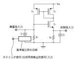
ゲート回路5の構成を図3Aに示す。ゲート回路5は、前段の層からの信号選択部50、クロック信号入力部51、カウンタ52、ゲートスイッチ53、ゲート制御回路54などから構成される。
The configuration of the
信号選択部50は、そのゲート回路5と対応する特徴検出層ニューロンの受容野に属する特徴統合層ニューロンからの信号のうち既に説明したような所定の基準を満たす信号だけを選択的に入力する。例えば、前段の特徴統合層ニューロン出力がメモリに一時的に格納される場合、受容野に属する各ニューロン出力が格納されているメモリアドレスを適切に設定する(例えば、上位k個の出力信号を選択する)ことにより信号の選択的入力を行う。以下、このような場合を前提として説明する。
The
ゲート回路のカウンタ52は、選択的に通過させたパルス信号数をカウントする為のものであり、クロック信号入力部51からのタイミング信号によりリセットされる。ゲート制御回路54は、カウンタ52の値が所定の上限値に達するとゲートスイッチ53を開き、以後パルス信号は後段の層に出力されない。
The
特徴検出層への信号の並列入力が時分割で部分的に行われる(例えば、ある特徴クラスを検出する特徴検出ニューロン全体の4分の1に対応する受容野分の特徴統合層からの信号を一度に入力する)場合には、制御回路は受容野が互いに重なり合わない特徴検出層ニューロンを並列入力可能な数だけ選択する。この場合、次にゲート制御回路の信号選択部50は各特徴検出層ニューロンの受容野に対応する特徴統合層ニューロン出力を格納するメモリアドレスを設定して各出力データを読み込む。上述した並列入力以降の入力ステップでは、受容野が互いに重なり合わない条件は保持しながら、前の入力ステップで入力したものと順次異なる受容野からの入力を行う。
Parallel input of signals to the feature detection layer is performed in a time-sharing manner (for example, signals from the feature integration layer corresponding to one-fourth of all feature detection neurons that detect a certain feature class In the case of inputting at the same time, the control circuit selects as many feature detection layer neurons whose receptive fields do not overlap each other as many as possible in parallel input. In this case, the
ゲート回路の信号選択部50は一般的に、通過させる信号の数kが1の場合、いわゆるWinner take all(WTA)回路としての機能を持つ。特徴統合層からの出力が位相変調されたパルス信号である場合には、信号のレベルを基準時刻からの遅延量によってその信号レベルを検出する。基準時刻は、全体制御回路7内部のタイミング素子からのクロックパルス信号の入力により与えられる。
The
ゲート回路は、図5に示す構成に限定されるものではなく、上述した信号選択機能を有するものであれば良いことは言うまでもない。なお、以上の説明では一つの特徴クラスについて一つのゲート回路を設定したが、特徴統合層の複数の特徴クラスからの信号について一括して上位レベルの出力信号(極大値信号であることを条件としても良い)を選択的に通過させても良い。この場合は、ある特徴クラスで上位レベル信号であっても複数クラスの全体としては上位ではない信号は、ゲート回路を通過できないことは言うまでもない。 Needless to say, the gate circuit is not limited to the configuration shown in FIG. 5 and may have any of the signal selection functions described above. In the above description, one gate circuit is set for one feature class. However, the signals from a plurality of feature classes in the feature integration layer are collectively output on the condition that they are high-level output signals (maximum value signals). May also be selectively passed. In this case, it is needless to say that a signal that is not a high-order signal as a whole of a plurality of classes even though it is a high-level signal in a certain feature class cannot pass through the gate circuit.
次にニューロン素子間の結合手段としてのシナプス回路について説明する。 Next, a synapse circuit as a coupling means between neuron elements will be described.
本実施形態でのシナプス回路は、層間結合を実現し、図7Aに示すように、神経細胞(ニューロン)の軸索または樹状突起に相当する信号伝達部(配線または遅延線)、及びシナプス結合部である。図7Aでは、ある特徴検出(統合)細胞に対する受容野を形成する特徴統合(検出)細胞のニューロン群(nj)からの出力(当該細胞から見ると入力)に関与する結合部の構成を示している。図7Aにおいて、各ニューロン素子njは、パルス信号列(スパイクトレイン)を出力する。 The synapse circuit in the present embodiment realizes interlayer coupling, and as shown in FIG. 7A, a signal transmission unit (wiring or delay line) corresponding to an axon or dendrite of a neuron (neuron), and synapse coupling Part. FIG. 7A shows a configuration of a connection part involved in an output (input as viewed from the cell) of a neuron group (n j ) of a feature integration (detection) cell that forms a receptive field for a certain feature detection (integration) cell. ing. In FIG. 7A, each neuron element n j outputs a pulse signal train (spike train).
いわゆる興奮性結合は、シナプス回路においてパルス信号の増幅を行い、抑制性結合は逆に減衰を与えるものである。パルス信号により情報の伝達を行う場合、増幅及び減衰はパルス信号の振幅変調、パルス幅変調、位相変調、周波数変調のいずれによっても実現することができる。 So-called excitatory coupling amplifies a pulse signal in a synaptic circuit, and inhibitory coupling conversely gives attenuation. When information is transmitted using a pulse signal, amplification and attenuation can be realized by any of amplitude modulation, pulse width modulation, phase modulation, and frequency modulation of the pulse signal.
本実施形態においては、シナプス結合部Sは、パルスの位相変調素子として用いる場合には、信号の増幅はパルス到着時間の実質的な進み(或いは、少ない位相遅延量)として、減衰は実質的な遅れ(或いは、大きな位相遅延量)として変換される。即ち、定性的には興奮性結合は、ある基準位相に対する到着パルスの位相の進みを、抑制性結合では同様に遅れを与えるものである。シナプス結合手段としては、この他にパルス幅変調、周波数変調などいずれの変調方法を用いても構わない(本実施形態では、パルス位相変調を用いて説明する)。シナプス結合部とニューロン素子とを、それぞれまとめて図7Bに示すような回路ブロックを構成してもよい。 In the present embodiment, when the synapse coupling unit S is used as a pulse phase modulation element, the signal amplification is a substantial advance of the pulse arrival time (or a small phase delay amount), and the attenuation is substantially It is converted as a delay (or a large phase delay amount). In other words, qualitatively excitatory coupling gives a phase advance of the arrival pulse with respect to a certain reference phase, and inhibitory coupling similarly gives a delay. As the synapse coupling means, any other modulation method such as pulse width modulation or frequency modulation may be used (this embodiment will be described using pulse phase modulation). The synapse connection unit and the neuron element may be combined to form a circuit block as shown in FIG. 7B.
次に、各層を構成するニューロン素子について説明する。各ニューロン素子はパルス信号を入力し、パルス信号を出力するパルス信号の変調出力素子であり、例えば入力信号(アクションポテンシャルに相当するパルス列)を時空間的に線形加算した結果が閾値を越したら発火し、パルス状信号を出力するようないわゆるintegrate-and-fireニューロン、或いはパルス信号の位相、幅などの非線形変換回路を用いても良い。 Next, neuron elements constituting each layer will be described. Each neuron element is a pulse signal modulation output element that inputs a pulse signal and outputs a pulse signal. For example, it fires when the result of linear addition of input signals (pulse trains corresponding to action potentials) exceeds the threshold A so-called integral-and-fire neuron that outputs a pulse signal or a non-linear conversion circuit such as the phase and width of the pulse signal may be used.
特徴検出層(1、k+1)の画像特徴部ニューロン素子は、入力として特徴統合層(2、k)の複数の特徴クラスに属するニューロン素子からの出力を受ける。 The image feature neuron elements in the feature detection layer (1, k + 1) receive outputs from neuron elements belonging to a plurality of feature classes in the feature integration layer (2, k) as inputs.
一方、特徴統合層(2、k+1)のニューロン素子は、そのニューロン素子と同じ特徴クラスに属する特徴検出層ニューロン素子からの出力を受ける。 On the other hand, the neuron element of the feature integration layer (2, k + 1) receives an output from the feature detection layer neuron element belonging to the same feature class as the neuron element.
図4は、ニューロン素子をIntegrate-and-fire回路としたときに用いられるニューロン素子のパルス発生回路の動作原理を表す基本構成の一例を示す。ここでは、3種類の入力として、特徴統合層または特徴検出層からの興奮性入力若しくは抑制性の入力、及び、全体制御回路7にあるタイミング素子からの入力を受けるものとして構成されている。3番目の入力信号は後述する時間窓の発生タイミング(入力パルス信号の時間積分開始のタイミング)信号を与えるためのものである。
FIG. 4 shows an example of a basic configuration representing an operation principle of a pulse generation circuit of a neuron element used when the neuron element is an Integrate-and-fire circuit. Here, three types of inputs are configured to receive an excitatory input or an inhibitory input from the feature integration layer or the feature detection layer and an input from a timing element in the
興奮性入力側のキャパシタC1及び抵抗R1回路の時定数は、キャパシタC2及び抵抗R2回路の時定数より小さく、定常状態では、トランジスタT1,T2,T3は遮断されている。なお、抵抗は実際には、能動負荷たるトランジスタで構成される。 The time constant of the capacitor C 1 and resistor R 1 circuit on the excitable input side is smaller than the time constant of the capacitor C 2 and resistor R 2 circuit, and the transistors T 1 , T 2 , T 3 are cut off in the steady state. . The resistor is actually composed of a transistor as an active load.
キャパシタC1の電位が増加し、キャパシタC2のそれよりトランジスタT1の閾値だけ上回ると、T1はアクティブになり、更にトランジスタT2,T3をアクティブにする。トランジスタT2,T3は、電流ミラー回路を構成し、図4の回路の出力は、不図示の出力回路によりキャパシタC1側から出力される。キャパシタC2の電荷蓄積量が最大となるとトランジスタT1は遮断され、その結果としてトランジスタT2及びT3も遮断され、上記正のフィードバックは0となる様に構成されている。
The potential of the capacitor C 1 increases and exceeds than that of the capacitor C 2 by the threshold value of the transistor T 1, T 1 becomes active, further activates the
いわゆる不応期にはキャパシタC2は放電し、C1の電位がC2の電位よりT1の閾値分より大とならない限り、ニューロンは応答しない。キャパシタC1,C2の交互充放電の繰り返しにより周期的なパルスが出力され、その周波数は一般的には興奮性入力のレベルに対応してきまる。但し、不応期が存在することにより、最大値で制限されるようにすることもできるし、一定周波数を出力するようにもできる。 Capacitor C 2 is the so-called refractory period is discharged, as long as the potential of the C 1 does not become larger than the threshold amount of T 1 than the potential of the C 2, neurons do not respond. Periodic pulses are output by repeating alternating charging and discharging of the capacitors C 1 and C 2 , and the frequency generally corresponds to the level of excitability input. However, since there is a refractory period, it can be limited by the maximum value, or a constant frequency can be output.
なお、上記Integrate-and-Fire機能を有する素子を用いず、シナプス後のパルス信号が加算された内部状態を所定のニューロン活性化関数(シグモイド関数など)に基づいて変調されたパルス信号のかたちで出力する回路を用いても良い。 In addition, without using the element with the above-mentioned Integrate-and-Fire function, the internal state where the post-synaptic pulse signal is added is converted into a pulse signal modulated based on a predetermined neuron activation function (such as a sigmoid function). An output circuit may be used.
ニューロン素子でのパルス信号積分特性を制御する役割をもつのが、時間窓重み関数発生回路である。この回路によりキャパシタの電位(及び電荷蓄積量)は時間的に制御される。この制御特性を反映するのが、入力パルスに対する後述の時間窓内での重み付き加算である(図11A〜図11Dを参照)。 The time window weight function generation circuit has a role of controlling the pulse signal integration characteristics in the neuron element. With this circuit, the potential of the capacitor (and the amount of accumulated charge) is temporally controlled. Reflecting this control characteristic is a weighted addition within the time window described later for the input pulse (see FIGS. 11A to 11D).
この重みにシナプス荷重値を対応させる場合には、時間窓重み関数発生回路は信号レベルとシナプス荷重値の積に相当する値が得られるように入力パルスの到着時間に応じた重み関数を生成する。即ち、パルスの到着時間の遅れ増大とともに乗算される重みの値が減少するように関数波形が設定される。関数波形の生成は、アナログ発振回路を使うか、デジタル回路でルックアップテーブル法や関数生成法によりデジタル波形を作り出し、それをD/A変換器によりアナログ波形にする方法を用いてもよい。 When a synaptic load value is associated with this weight, the time window weight function generation circuit generates a weight function corresponding to the arrival time of the input pulse so that a value corresponding to the product of the signal level and the synaptic load value is obtained. . That is, the function waveform is set so that the weight value to be multiplied decreases as the arrival time of the pulse increases. For generating the function waveform, an analog oscillation circuit may be used, or a digital waveform may be generated by a digital circuit by a look-up table method or a function generation method, and converted to an analog waveform by a D / A converter.
この基準電圧制御回路は、タイミング素子からの入力タイミング(又は、後続層のニューロンとの相互結合入力)に基づき、基準電圧信号(図11Bの重み関数に相当)を発生する。 The reference voltage control circuit generates a reference voltage signal (corresponding to the weight function in FIG. 11B) based on the input timing from the timing element (or the mutual coupling input with the neurons in the subsequent layer).
一般的に、入力信号の上記総和と出力レベル(パルス位相、パルス周波数、パルス幅など)の関係は、そのニューロンの感度特性によって変化し、また、その感度特性は上位層からのトップダウンの入力により変化させることができる。以下では、説明の便宜上、入力信号総和値に応じたパルス出力の周波数は急峻に立ち上がるように回路パラメータが設定されているものとし(従って周波数ドメインでは殆ど2値)、パルス位相変調により、出力レベル(位相変調を与えたタイミングなど)が変動するものとする。 In general, the relationship between the above sum of input signals and the output level (pulse phase, pulse frequency, pulse width, etc.) varies depending on the sensitivity characteristics of the neuron, and the sensitivity characteristics are top-down inputs from higher layers. Can be changed. In the following, for convenience of explanation, it is assumed that the circuit parameters are set so that the frequency of the pulse output corresponding to the total value of the input signal rises sharply (thus almost binary in the frequency domain), and the output level is obtained by pulse phase modulation. It is assumed that the timing (such as the timing at which phase modulation is applied) varies.
特徴統合層内の画像特徴部ニューロンからの出力により、時間窓内の重み関数で上記基準電圧が制御される結果、特徴検出層ニューロンからの出力特性(例えばパルス出力の位相)が変化する。位相変調がなされる場合には、この位相をニューロンの出力レベルとして用いることができる。 As a result of the output from the image feature neuron in the feature integration layer, the reference voltage is controlled by the weighting function in the time window, and as a result, the output characteristics (for example, the phase of pulse output) from the feature detection layer neuron change. When phase modulation is performed, this phase can be used as the output level of the neuron.
また、ニューロン出力(シナプス前)の位相は、後述するように時間窓の始期を基準とし、その基準時からの遅れ(位相)は基準パルス(タイミング素子出力その他による)を受けた時の電荷蓄積量により決まるような出力特性を有する。このような出力特性を与える回路構成の詳細については、本実施形態の主眼とする所ではないので省略する。シナプス後のパルス位相が当該シナプスにより与えられる固有の位相変調量にシナプス前の位相を加算したものとする場合には、シナプス荷重とシナプス前信号との乗算(通常行われる演算)は、後述する時間窓重み関数において行われる。 The phase of the neuron output (before synapse) is based on the start of the time window as described later, and the delay (phase) from the reference time is the charge accumulation when receiving the reference pulse (due to the timing element output and others). The output characteristic is determined by the quantity. The details of the circuit configuration that provides such output characteristics are not the main points of the present embodiment, and will be omitted. When the post-synaptic pulse phase is obtained by adding the pre-synaptic phase to the intrinsic phase modulation amount given by the synapse, multiplication of the synaptic load and the pre-synaptic signal (a calculation that is normally performed) will be described later. This is done in the time window weight function.
なお、窓関数などを用いることにより得られる入力の総和値が閾値を越えたときに、所定タイミング遅れて発振出力を出すような公知の回路構成を用いてもよい。 It should be noted that a known circuit configuration may be used in which an oscillation output is output with a predetermined timing delay when the total value of inputs obtained by using a window function or the like exceeds a threshold value.
特徴検出層のニューロンは前述したように特徴カテゴリに応じた受容野構造を有し、前段の層(入力層または特徴統合層)のニューロンからの入力パルス信号(電流値または電位)の時間窓関数による後述の荷重総和値が閾値以上となったとき、その総和値に応じて、例えばシグモイド関数等の一定レベルに漸近的に飽和するような非減少かつ非線形な関数、即ちいわゆるsquashing関数値をとるような出力(ここでは位相変化で与える;周波数、振幅、パルス幅基準での変化となる構成でもよい)でパルス出力を行う。 The neuron of the feature detection layer has a receptive field structure corresponding to the feature category as described above, and the time window function of the input pulse signal (current value or potential) from the neuron of the previous layer (input layer or feature integration layer) When the total load value (described later) is equal to or greater than the threshold, a non-decreasing and non-linear function that is asymptotically saturated to a certain level such as a sigmoid function, that is, a so-called squashing function value is taken. The pulse is output with such an output (in this case, it is given by phase change; the change may be based on frequency, amplitude, and pulse width).
<シナプス回路等>
図4は、シナプス結合部Siにおいてニューロンniの結合先である各ニューロンn’jへのシナプス結合強度(位相遅延等に関する変調の大きさを意味する)を与える各小回路がマトリクス的に配置されていることを示す。
<Synapse circuit, etc.>
FIG. 4 shows that each small circuit that gives synapse connection strength (meaning the magnitude of modulation related to phase delay or the like) to each neuron n ′ j to which the neuron ni is connected in the synapse connection portion Si is arranged in a matrix. Indicates that
図9Bに示すように各シナプス結合小回路401は、学習回路402と位相遅延回路403とからなる。学習回路402は、位相遅延回路403の特性を変化させることにより、上記遅延量を調整し、また、その特性値(或いはその制御値)を浮遊ゲート素子、或いは浮遊ゲート素子と結合したキャパシタ上に記憶するものである。
As shown in FIG. 9B, each
位相遅延回路403はパルス位相変調回路であり、例えば、図10Aに示すような単安定マルチバイブレータ506、507及び、抵抗501、504、キャパシタ503、505、トランジスタ502を用いた構成がある。図10Bは単安定マルチバイブレータ506へ入力された方形波P1、単安定マルチバイブレータ506から出力される方形波P2、単安定マルチバイブレータ507から出力される方形波P3の各タイミングを表している。
The
位相遅延回路403の動作機構の詳細については説明を省略するが、P1のパルス幅は、充電電流によるキャパシタ503の電圧が予め定められた閾値に達するまでの時間で決まり、P2の幅は抵抗504とキャパシタ505による時定数で決まる。P2のパルス幅が(図10Bの点線方形波のように)広がって、その立ち下がり時点が後にずれるとP3の立ち上がり時点も同じ量ずれるが、P3のパルス幅は変わらないので、結果的に入力パルスの位相だけが変調されて出力されたことになる。
Although a detailed description of the operation mechanism of the
位相遅延量は、シナプス結合に入力される前のパルス信号とシナプス結合後のパルス信号とでシナプス荷重に相当する位相遅延の変換により与えられる。本実施形態では、シナプス荷重値が大きいほど小さい位相遅延量になるようにする。 The phase delay amount is given by the conversion of the phase delay corresponding to the synaptic load between the pulse signal before being input to the synapse connection and the pulse signal after the synapse connection. In this embodiment, the larger the synapse load value, the smaller the phase delay amount.
なお、シナプス結合回路としては位相遅延回路を用いる代わりに後述する所定の重み関数を用いた時間窓積分回路を用いても良い。この場合は、パルス信号にシナプス荷重に相当する重みがパルス信号に乗算されるように構成する。 As the synapse coupling circuit, a time window integrating circuit using a predetermined weight function described later may be used instead of using the phase delay circuit. In this case, the pulse signal is configured to be multiplied by a weight corresponding to the synaptic load.
制御電圧Ecを基準電圧のリフレッシュ回路509と結合荷重を与えるキャパシタ508への電荷蓄積量制御を行う学習回路402で変化させることにより、パルス位相(遅延量)を制御することができる。この結合荷重の長期保持のためには、学習動作後に不図示の浮遊ゲート素子等のアナログメモリへ、或いはデジタルメモリ(SDRAM,MRAMなど)への書き込み等を行って結合荷重を格納してもよい。
The pulse phase (delay amount) can be controlled by changing the control voltage E c by the
パルスの同時到着、或いは所定の位相変調量を実現するシナプスでの学習回路の例としては、図9Aに示すような回路要素を有するものを用いればよい。即ち、学習回路402をパルス伝播時間計測回路510(ここで、伝播時間とは、ある層のニューロンの前シナプスでのパルス出力時刻と次の層上にある出力先ニューロンでの当該パルスの到着時刻との時間差をさす)、時間窓発生回路511、及び伝播時間が一定値となるようにシナプス部でのパルス位相変調量を調整するパルス位相変調量調整回路512から構成できる。
As an example of a learning circuit at a synapse that realizes simultaneous arrival of pulses or a predetermined phase modulation amount, a learning circuit having a circuit element as shown in FIG. 9A may be used. That is, the
伝播時間計測回路510としては、後述するような同一局所受容野を形成するタイミング素子からのクロックパルスを入力し、所定の時間幅(時間窓:図3B参照)において、そのクロックパルスのカウンタ回路からの出力に基づき伝播時間を求めるような構成などが用いられる。 As the propagation time measuring circuit 510, a clock pulse from a timing element that forms the same local receptive field as described later is input, and in a predetermined time width (time window: see FIG. 3B), from the counter circuit of the clock pulse. For example, a configuration in which the propagation time is obtained based on the output of is used.
<特徴検出層(1,0)での処理>
特徴検出層10の各ニューロンは、gmnに対応する受容野構造を有する。同じスケールインデックスmを有するgmnは同じサイズの受容野を有し、演算上は対応するカーネルgmnサイズもスケールインデックスに応じた大きさを有するようにしてある。ここでは、最も粗いスケールから順に入力画像上の30×30、15×15、7×7のサイズとした。各ニューロンは、分布重み係数と画像データとの積和入力を行って得られるウエーブレット変換係数値の非線型squashing関数となる出力レベル(ここでは位相基準とする;但し、周波数、振幅、パルス幅基準となる構成でもよい)でパルス出力を行う。この結果、この層(1,0)全体の出力として、Gabor wavelet変換が行われたことになる。
<Processing in the feature detection layer (1, 0)>
Each neuron of the feature detection layer 10 has a receptive field structure corresponding to gmn . G mn having the same scale index m has receptive fields of the same size, and the corresponding kernel g mn size is calculated so as to have a size corresponding to the scale index. Here, the sizes of the input image are 30 × 30, 15 × 15, and 7 × 7 in order from the coarsest scale. Each neuron has an output level that is a nonlinear squashing function of wavelet transform coefficient values obtained by performing product-sum input of distribution weight coefficients and image data (here, phase reference; however, frequency, amplitude, pulse width) The pulse may be output with a reference configuration. As a result, Gabor wavelet conversion is performed as an output of the entire layer (1, 0).
<特徴検出層での処理(中次、高次特徴抽出)>
後続の特徴検出層((1,1)、(1,2)、・・・)では、中次から高次の画像特徴を入力画像上の所定サンプリング位置で検出する。各ニューロンは、上記特徴検出層(1,0)とは異なり、検出すべき特徴パターンに固有の受容野構造をいわゆるHebb学習則等により形成する。後の層ほど特徴検出を行う局所的な領域のサイズが認識対象全体のサイズに段階的に近くなり、幾何学的には中次または高次の特徴を検出する。例えば、顔の検出認識を行う場合には中次(または高次)の特徴とは顔を構成する目、鼻、口等の図形要素のレベルでの特徴を表す。なお、特徴検出層ニューロンは一般的に(低次、高次特徴抽出に依らず)、出力の安定化のために抑制性(分流型抑制:shunting inhibition)の結合を前段の層出力に基づいて受けるような機構を有してもよい。
<Processing in the feature detection layer (middle order and higher order feature extraction)>
In the subsequent feature detection layer ((1, 1), (1, 2),...), The middle to higher order image features are detected at predetermined sampling positions on the input image. Each neuron, unlike the feature detection layer (1, 0), forms a receptive field structure specific to the feature pattern to be detected by a so-called Hebb learning rule. The size of the local region where the feature detection is performed becomes closer to the size of the entire recognition target stepwise in the later layers, and a medium-order or higher-order feature is detected geometrically. For example, when detecting and recognizing a face, the middle-order (or higher-order) feature represents a feature at the level of graphic elements such as eyes, nose and mouth constituting the face. In general, feature detection layer neurons (regardless of low-order or high-order feature extraction) are connected based on the output of the previous layer in order to stabilize the output. You may have a mechanism which receives.
<特徴統合層(画像特徴部)での処理>
特徴統合層((2,0)、(2,1)、・・・)のニューロン素子について説明する。図2に示すごとく特徴検出層(例えば(1,0))から特徴統合層(例えば(2,0))への結合は、当該特徴統合ニューロンの受容野内にある前段の特徴検出層の同一特徴要素(タイプ)のニューロン素子から興奮性結合の入力及び後述するタイミング素子出力(PNout1)をともに図4の興奮性入力側で受けるように構成され、統合層のニューロン素子の機能は前述したごとく、特徴カテゴリごとの局所平均化或いは最大値検出その他のサブサンプリング等である。
<Processing in the feature integration layer (image feature part)>
A neuron element of the feature integration layer ((2, 0), (2, 1),...) Will be described. As shown in FIG. 2, the connection from the feature detection layer (for example, (1, 0)) to the feature integration layer (for example, (2, 0)) is the same feature of the preceding feature detection layer in the receptive field of the feature integration neuron. An excitatory coupling input and a timing element output (PNout1) described later are received on the excitatory input side of FIG. 4 from the element (type) neuron element, and the function of the neuron element of the integration layer is as described above. For example, local averaging for each feature category or maximum value detection or other sub-sampling.
特徴統合層ニューロンによれば、複数の同一種類の特徴に関するパルスを入力し、それらを局所的な領域(受容野)で統合して平均化する(或いは、受容野内での最大値等の代表値を算出する)ことにより、その特徴の位置のゆらぎ、変形に対しても確実に検出することができる。このため、特徴統合層ニューロン素子の受容野構造は、特徴カテゴリによらず一様(例えば、いずれも所定サイズの矩形領域であって、かつ感度または重み係数がその中で一様分布するなど)となるように構成してよい。 According to the feature integration layer neuron, a plurality of pulses related to the same type of feature are input, and they are integrated in a local region (receptive field) and averaged (or a representative value such as a maximum value in the receptive field). Thus, it is possible to reliably detect fluctuations and deformations of the feature position. For this reason, the receptive field structure of the feature integration layer neuron element is uniform regardless of the feature category (for example, each is a rectangular region of a predetermined size and the sensitivity or weighting coefficient is uniformly distributed therein). You may comprise so that it may become.
<パターン検出の動作原理>
以下、図2に示すネットワーク構成をパターン認識装置に適用する場合の2次元図形パターンのパルス符号化と検出方法について説明する。図8Aは、特徴統合層から特徴検出層への(例えば、図1の層(2,0)から層(1,1)への)パルス信号の伝播の様子を模式的に示したものである。ゲート回路5がシナプス結合素子(Sj)の前にあり、特徴検出に有意なパルス信号(P1,P3)のみを通過させることを示している。図8Aではシナプス結合素子S1,S3により変調を受けるパルスのみが伝播することを示している。特徴統合層側の各ニューロンniは、それぞれ異なる特徴量(或いは特徴要素)に対応し、特徴検出層側のニューロンn’jは、同一受容野内の各特徴を組み合わせて得られる、より高次の特徴(図形要素)の検出に関与する。
<Principle of pattern detection>
Hereinafter, a pulse encoding and detection method for a two-dimensional figure pattern when the network configuration shown in FIG. 2 is applied to a pattern recognition apparatus will be described. FIG. 8A schematically shows how a pulse signal propagates from the feature integration layer to the feature detection layer (for example, from the layer (2,0) to the layer (1,1) in FIG. 1). . The
特徴統合層ニューロンから特徴検出層ニューロンへの結合により特徴統合層出力の上位レベルのみ伝達させるために、上位レベルの極大値をとるパルス信号についてだけ開くゲート回路5をシナプス結合回路の入力側に設定してある。
タイミングパルス信号(PN)入力があったときに、特徴統合層ニューロンからの出力パルス信号は、シナプス結合回路で位相変調などの変調処理を受けて次の特徴検出層に伝播し、特徴検出層ニューロンでは特徴統合層ニューロンからのシナプス結合を経由したパルス信号の時間的積分が時間積分窓の範囲内で行われる。
In order to transmit only the upper level of the feature integration layer output by coupling from the feature integration layer neuron to the feature detection layer neuron, the
When there is a timing pulse signal (PN) input, the output pulse signal from the feature integration layer neuron is subjected to modulation processing such as phase modulation in the synapse connection circuit and propagates to the next feature detection layer, and the feature detection layer neuron Then, temporal integration of pulse signals via synaptic connections from feature integration layer neurons is performed within the range of the time integration window.
ここに、時間窓は特徴検出細胞(n’i)ごとに定められ、当該細胞に関して同一受容野を形成する特徴統合層内の各ニューロンに対して共通であり、時間窓積分の時間範囲を与える。 Here, a time window is defined for each feature detection cell (n′i), and is common to each neuron in the feature integration layer forming the same receptive field with respect to the cell, giving a time range for time window integration. .
図8Aではゲート回路5は、特徴検出層ニューロンのシナプス結合の前にある。ゲート回路5に信号を入力するニューロンは、特徴検出層ニューロンの受容野を構成し、かつ同じ特徴クラスに属する全ての特徴統合層ニューロンである。本実施形態での特徴検出層ニューロンは、ゲート回路5を通過後の各パルス信号の時間窓積分を並列的に行う。図8Bはこのときのシナプス後の信号が並列的に時間窓積分される様子(ほぼ同じ時間帯に複数の時間窓積分を行う様子)を模式的に表す。
In FIG. 8A, the
タイミング素子は、全体制御回路7にあって、タイミングパルス信号を層番号(2,k−1)の各特徴統合細胞、及び各特徴検出細胞(層番号(1,k))に出力することにより、特徴検出細胞が時間的に入力を加算する際の時間窓発生のタイミング信号を与えている。この時間窓の開始時刻が各特徴統合細胞から出力されるパルスの到着時間を図る基準時となる。即ち、タイミング素子は特徴統合細胞からのパルス出力時刻、及び特徴検出細胞での時間窓積分の基準パルスを与える。
The timing element is in the
本実施形態では、特徴検出層の前段の層である特徴統合層上の同一受容野内の各低次特徴要素に相当するニューロンであって入力画像中において所定の局所的特徴の検出に関与したものは、それぞれ所定の位相で同期発火(パルス出力)することになる。一般的に特徴統合層のニューロンであって位置が異なるが同一の高次の特徴を検出する特徴検出ニューロンへの結合が存在する(この場合、受容野は異なるが、高次の同じ特徴を構成する結合を有する)。この時、これら特徴検出ニューロンとの間でも同期発火することはいうまでもない。 In this embodiment, neurons corresponding to each low-order feature element in the same receptive field on the feature integration layer, which is the previous stage of the feature detection layer, are involved in detection of a predetermined local feature in the input image. Are synchronously fired (pulse output) at a predetermined phase. Generally, there is a connection to a feature detection neuron that detects the same higher-order feature in a feature integration layer that is located at different positions (in this case, the receptive field is different, but the same higher-order feature is configured) To have a bond). At this time, it goes without saying that synchronous firing occurs between these feature detection neurons.
各パルスはシナプス回路を通過すると所定量の位相遅延が与えられ、更に信号伝達線を通って特徴検出細胞に到着する。パルスの時間軸上の並びを、特徴検出細胞の時間軸上において点線で表したパルス(P1,P2,P3)により示す。 Each pulse is given a predetermined amount of phase delay when passing through the synapse circuit, and further reaches the feature detection cell through the signal transmission line. The arrangement of the pulses on the time axis is indicated by pulses (P1, P2, P3) represented by dotted lines on the time axis of the feature detection cells.
特徴検出細胞において各パルス(P1,P2,P3)の時間窓積分(通常、一回の積分とする;但し、多数回にわたる時間窓積分による電荷蓄積、または平均化処理を行ってもよい)の結果、閾値より大となった場合には、時間窓の終了時刻を基準としてパルス出力(Pd)がなされる。なお、同図に示した学習時の時間窓とは、後で説明する学習則を実行する際に参照されるものである。 Time-window integration of each pulse (P1, P2, P3) in the feature detection cell (usually a single integration; however, charge accumulation or averaging processing may be performed by multiple time-window integrations) As a result, when it becomes larger than the threshold value, a pulse output (Pd) is made with reference to the end time of the time window. The learning time window shown in the figure is referred to when a learning rule described later is executed.
<特徴検出層処理>
以下、特徴検出層で主に行われる処理(学習時、認識時)について説明する。各特徴検出層においては、前述したようにスケールレベルごとに設定される処理チャネル内において同一受容野からの複数の異なる特徴に関するパルス信号を入力し、時空間的重み付き総和(荷重和)演算と閾値処理を行う。
<Feature detection layer processing>
Hereinafter, processing mainly performed in the feature detection layer (during learning and recognition) will be described. In each feature detection layer, as described above, pulse signals relating to a plurality of different features from the same receptive field are input in a processing channel set for each scale level, and a spatio-temporal weighted sum (load sum) calculation is performed. Perform threshold processing.
また、特徴検出層上の各ニューロンにおいては入力パルスの時空間的重み付き総和(荷重和)の演算は、ニューロンに到着したパルス列について所定幅の時間窓においてのみ行われる。時間窓内の重み付き加算を実現する手段は、図4に示したニューロン素子回路に限らず、他の方法で実現してもよいことは言うまでもない。 In each neuron on the feature detection layer, the spatio-temporal weighted sum (load sum) of the input pulses is calculated only in a time window having a predetermined width with respect to the pulse train arriving at the neuron. Needless to say, means for realizing weighted addition within the time window is not limited to the neuron element circuit shown in FIG.
この時間窓は、実際のニューロンの不応期(refractory period)以外の時間帯にある程度対応している。即ち、不応期(時間窓以外の時間範囲)にはどのような入力を受けてもニューロンからの出力はないが、その時間範囲以外の時間窓では入力レベルに応じた発火を行うという点が実際のニューロンと類似している。 This time window corresponds to some extent to a time zone other than the actual neuronal refractory period. In other words, in the refractory period (time range other than the time window), there is no output from the neuron no matter what input is received, but in the time window outside that time range, firing is performed according to the input level. Similar to neurons.
本実施形態では、各層での処理に共通して制御回路内にあるタイミング素子(固定周波数でパルス出力)からのタイミングパルス信号を入力することにより、上述した時間窓開始時期のニューロン間での共通化をもたらしている。図1に示すような構成において、シナプスアレイ回路ブロック3とニューロンアレイ回路ブロック2を図2に示す階層構造全体の一層分とすると、タイミング信号は層内で共通して用いられる。また、シナプスアレイ回路ブロック3とニューロンアレイ回路ブロック2を図2に示す階層構造全体のうち一部に相当する複数の層が実現されるように構成した場合であっても、時間窓の同期制御は(仮に必要であったとしても)ネットワーク全体にわたって行う必要は無く、タイミング信号のskew等の問題は全体として緩和されている。
In this embodiment, the timing pulse signal from the timing element (pulse output at a fixed frequency) in the control circuit is input in common to the processing in each layer, so that the time window start timing described above is shared among neurons. Has brought about. In the configuration as shown in FIG. 1, if the synapse
<撮像装置、ロボット視覚ヘッドなどへ搭載した応用例>
本実施形態の構成に係る並列パルス信号処理手段をパターン認識(検出)装置としてロボット視覚ヘッド、或いは光軸方向制御機構を有する撮像装置に搭載させることにより、視野内の特定被写体を高速に検出し、最適撮影(自動フォーカシングや特定被写体の色補正、露出等)制御を行うことができる。この場合の構成について、図12を参照して説明する。
<Application examples installed in imaging devices, robot vision heads, etc.>
By mounting the parallel pulse signal processing means according to the configuration of the present embodiment as a pattern recognition (detection) device on a robot vision head or an imaging device having an optical axis direction control mechanism, a specific subject in the field of view can be detected at high speed. Optimal shooting (automatic focusing, color correction of specific subject, exposure, etc.) can be controlled. The configuration in this case will be described with reference to FIG.
図12の撮像装置9は、撮影レンズおよびズーム撮影及び光軸方向制御用の駆動制御機構を含む結像光学系92、CCD又はCMOSイメージセンサー93、撮像パラメータの計測手段94、映像信号処理回路95、記憶手段96、撮像動作の制御、撮像条件の制御などの制御用信号を発生する制御信号発生手段97、EVFなどファインダーを兼ねた表示ディスプレイ98、ストロボ発光手段99、記録媒体910、そして注視認識処理手段911(上述した本実施形態での階層構造を持った並列パルス信号処理回路からなるパターン認識装置)などを具備する。
The
この撮像装置は、撮像手段内の映像センサから入力される画像信号から予め登録された人物の存在する方向を推定し、当該方向へ撮像光学系の光軸制御を行って顔画像の検出(存在位置、サイズの検出)を注視認識処理手段911により行う。その人物の位置(存在方向)、サイズ情報は制御信号発生手段に97に入力されると、同制御信号発生手段97は、撮像パラメータ計測手段94からの出力に基づき、その人物に対するピント制御、露出条件制御、ホワイトバランス制御などを最適に行う制御信号を発生する。 This imaging device estimates the direction in which a pre-registered person exists from an image signal input from a video sensor in the imaging means, detects the face image by performing optical axis control of the imaging optical system in that direction (existence) (Detection of position and size) is performed by the gaze recognition processing means 911. When the position (existing direction) and size information of the person are input to the control signal generation means 97, the control signal generation means 97 performs focus control and exposure for the person based on the output from the imaging parameter measurement means 94. A control signal for optimally performing condition control, white balance control, etc. is generated.
上述した実施形態に係る並列パルス信号処理装置をこのように画像からパターン検出(認識)を行う撮像装置に用いることにより、当該被写体の検出(認識)機能を確実に、低消費電力で、かつ高速(リアルタイム)に実現して、人物等の検出とそれに基づく撮影の最適制御(AF、AEなど)を行うことができる。 By using the parallel pulse signal processing device according to the above-described embodiment in an imaging device that performs pattern detection (recognition) from an image in this way, the subject detection (recognition) function can be ensured, with low power consumption and high speed. (Real-time) can be performed to detect a person or the like and perform optimal control (AF, AE, etc.) of shooting based on the detection.
[第2の実施形態]
本実施形態では、ニューロン素子へのパルス信号は、シナプス結合後の各信号を束ねて伝播する為の共通バスラインを通じて入力され、特徴検出層ニューロンに対しては、前段の特徴統合層出力のうち、特徴クラスに固有の位相変調を受けたパルスが時系列的に入力される。ゲート回路5をシナプス結合回路の後方であってシナプス結合が収束する共通バスライン上に設定する。
[Second Embodiment]
In the present embodiment, the pulse signal to the neuron element is input through a common bus line for bundling and propagating each signal after synapse connection, and for the feature detection layer neuron, of the output of the feature integration layer in the previous stage. The pulses subjected to phase modulation specific to the feature class are input in time series. The
本実施形態で用いるゲート回路の構成を図6に示す。ゲート回路5は、前段の層からの信号選択部510、クロック信号入力部511、カウンタ512、ゲートスイッチ513、ゲート制御回路514、遅延時間ベースでの比較器515などから構成される。ここでの信号選択部510は、処理結果保持メモリ4にアクセスして、受容野からの信号を取り出すためのものであり、いわゆるWTA的な機能は有しない。
The configuration of the gate circuit used in this embodiment is shown in FIG. The
一方、比較器515はタイミング素子から与えられる基準時刻に対する到着パルス時刻の遅延量に基づいて上位レベルの信号(或いは上位レベルの極大値信号)だけを選択するための回路で時間軸ドメインでのWTA回路とみなすことができる。その他の構成要素の機能は、第1の実施形態で説明した図3Aに示す構成の各要素と同様である。 On the other hand, the comparator 515 is a circuit for selecting only an upper level signal (or an upper level maximum value signal) based on the delay amount of the arrival pulse time with respect to the reference time given from the timing element, and is a WTA in the time axis domain. It can be regarded as a circuit. The functions of the other constituent elements are the same as those of the constituent elements shown in FIG. 3A described in the first embodiment.
図8Cでは、各ニューロン間結合には、パルスの伝播時間とニューロンniからニューロンn’jへのシナプス結合(Sj,i)での時間遅れ等による固有(特徴に固有)の遅延が生じ、その結果としてニューロンn’jに到着するパルス列Piは、特徴統合層の各ニューロンからパルス出力がなされる限り、学習によって決まるシナプス結合での遅延量により、所定の順序(及び間隔)になっている(図8Cでは、P4,P3,P2,P1の順に到着するように示されている)。ゲート回路5は、シナプス結合により変調を受け、共通バス上を伝播するパルス列に対して上述したように選択的にパルス信号を通す。
In FIG. 8C, each interneuron connection has an inherent (feature-specific) delay due to a pulse propagation time and a time delay at the synaptic connection (S j, i ) from neuron ni to neuron n ′ j . As a result, the pulse train P i arriving at the neuron n ′ j is in a predetermined order (and interval) depending on the delay amount at the synaptic connection determined by learning as long as pulse output is made from each neuron of the feature integration layer. (In FIG. 8C, they are shown to arrive in the order of P4, P3, P2, and P1). The
図8Dは、タイミング信号が特徴統合層ニューロンに入力された後についての層番号(2,k)上の特徴統合細胞n1、n2、n3(それぞれ異なる種類の特徴を表す)から、層番号(1,k+1)上のある特徴検出細胞(n’j)(より上位の特徴検出を行う)へのパルス伝播のタイミング等を示す。 FIG. 8D shows from the feature integrated cells n 1 , n 2 , n 3 (each representing a different type of feature) on the layer number (2, k) after the timing signal is input to the feature integrated layer neuron. The timing of pulse propagation to a certain feature detection cell (n ′ j ) (which performs higher-order feature detection) on the number (1, k + 1) is shown.
特徴検出層ニューロンの内部状態の算出処理は、所定の重み付き時間窓積分により行われる。図8Cにおいて、特徴検出層ニューロンでは、タイミング素子からの入力がある前は後述する時間窓積分は行われず、タイミング素子からのパルス入力をトリガーとして、同積分が行われる。 The calculation process of the internal state of the feature detection layer neuron is performed by a predetermined weighted time window integration. In FIG. 8C, in the feature detection layer neuron, time window integration described later is not performed before the input from the timing element, and the integration is performed using a pulse input from the timing element as a trigger.
図8Cに示す不応期は、特徴検出細胞の発火直後から次の時間窓開始時刻までの時間帯である。不応期の長さと時間窓の幅は任意に設定可能であることはいうまでもなく、同図に示したように時間窓に比べて不応期を短くとらなくてもよい。 The refractory period shown in FIG. 8C is a time period from immediately after the firing of the feature detection cell to the next time window start time. It goes without saying that the length of the refractory period and the width of the time window can be arbitrarily set, and the refractory period does not have to be shorter than the time window as shown in FIG.
各特徴量に対応するパルスは予め学習により定められた遅延量(位相)により、所定の時間間隔で到着する。このパルス到着時間パターンの学習制御は、本実施形態の主眼ではないので詳しくは説明しないが、例えば、ある図形パターンを構成する特徴要素がその図形の検出に最も寄与する特徴であるほど先に到着し、そのままでは、パルス到着時間がほぼ等しくなる特徴要素間では、互いに一定量だけ時間的に離れて到着するような競争学習を導入する。或いは、予め決められた特徴要素(認識対象を構成する特徴要素であって、特に重要と考えられるもの:例えば、平均曲率の大きい特徴、直線性の高い特徴など)間で異なる時間間隔で到着する様に設計してもよい。 Pulses corresponding to each feature amount arrive at predetermined time intervals by a delay amount (phase) determined in advance by learning. This learning control of the pulse arrival time pattern is not the main focus of the present embodiment and will not be described in detail. For example, the feature element that constitutes a certain graphic pattern arrives earlier as the feature that contributes most to the detection of that graphic pattern. However, competitive learning that introduces a certain amount of time apart from each other is introduced between the feature elements that have almost the same pulse arrival times. Alternatively, it arrives at different time intervals between predetermined feature elements (feature elements constituting the recognition target, which are considered to be particularly important: for example, features with a large average curvature, features with high linearity, etc.) You may design it like this.
<パルス出力の時空間的統合及びネットワーク特性>
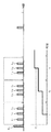
次に入力パルスの時空間的重み付き総和(荷重和)の演算について説明する。図11Bに示すごとく、各ニューロンでは、上記サブ時間窓(タイムスロット毎に所定の重み関数で入力パルスの荷重和がとられ、各荷重和の総和が閾値と比較される。τjはサブ時間窓jの重み関数の中心位置を表し、時間窓の開始時刻基準(開始時間からの経過時間)で表す。重み関数は一般に所定の中心位置(検出予定の特徴が検出された場合のパルス到着時間を表す)からの距離(時間軸上でのずれ)の関数になる。
<Spatio-temporal integration of pulse output and network characteristics>
Next, the calculation of the spatiotemporal weighted sum (load sum) of the input pulse will be described. As shown in FIG. 11B, in each neuron, the load sum of the input pulse is calculated with a predetermined weight function for each time slot, and the total sum of the load sums is compared with a threshold. Τ j is a sub time. Represents the center position of the weight function of the window j and is represented by the time window start time reference (elapsed time from the start time) The weight function is generally a predetermined center position (pulse arrival time when a feature to be detected is detected). It is a function of the distance (deviation on the time axis).
シナプスで特徴の種類に応じた位相変調が行われ、シナプス荷重値と信号との乗算が行われない場合には、時間窓積分において前段の層でのニューロン出力レベルにシナプス荷重に応じた乗算を時間軸上の重み関数値を参照して行う。 When phase modulation is performed according to the type of feature at the synapse and multiplication of the synapse load value and the signal is not performed, multiplication according to the synapse load is applied to the neuron output level in the previous layer in time window integration. Referring to the weight function value on the time axis.
なお、各サブ時間窓内での重み関数形状が対称の場合、若しくは時間軸上での距離の関数となっている場合、ニューロンの各サブ時間窓(タイムスロット)の重み関数の中心位置τが、ニューロン間の学習後の時間遅れとすると、入力パルスの時空間的重み付き総和(荷重和)を行う神経回路網は一種の時間軸ドメインのRadial Basis Function Network(以下RBFと略す)とみなすことができる。 When the weight function shape in each sub time window is symmetric, or when it is a function of the distance on the time axis, the center position τ of the weight function of each sub time window (time slot) of the neuron is Assuming time delay after learning between neurons, the neural network that performs spatio-temporal weighted summation (weighted sum) of input pulses is regarded as a kind of time-domain domain radial basis function network (hereinafter abbreviated as RBF). Can do.
重み関数としては、非対称形状(図11Bに示すように)や負の値をとるものであってもよい。例えば、ある特徴検出層のニューロンが三角形を最終的に検出することが予定されている場合に、その図形パターンの構成要素でないことが明らかな特徴(Ffalse)が検出された場合には、他の特徴要素からの寄与が大きくても三角形の検出出力が最終的になされないように、入力の総和値算出処理において、当該特徴(Ffalse)に対応するパルスからは、負の寄与を与えるような重み関数及び特徴検出(統合)細胞からの結合を与えておくことができる。 The weight function may be an asymmetric shape (as shown in FIG. 11B) or a negative value. For example, when a neuron of a certain feature detection layer is scheduled to finally detect a triangle, and a feature (F false ) that is clearly not a component of the graphic pattern is detected, In the input summation value calculation process, a negative contribution is given from the pulse corresponding to the feature (F false ) so that the triangle detection output is not finally made even if the contribution from the feature element is large . New weight functions and feature detection (integrated) connections from cells.
特徴検出層のニューロンniへの入力信号の時空間和Xi(t)は、 The spatio-temporal sum X i (t) of the input signals to the neurons n i of the feature detection layer is
![]()
![]()
ここに、εjは、ニューロンnjからの出力パルスの初期位相、FTiは時間窓重み関数であり、ニューロンniとの同期発火により、0に収束するか、又はタイミングパルス入力により、時間窓の位相を0に強制同期する場合には、εjは常に0としてよい。
図11Aのパルス入力と図11Bに示す重み関数による荷重和を実行すると、図11Dに示すような荷重和値の時間的遷移が得られる。特徴検出ニューロンは、この荷重和値が閾値(Vt)に達するとパルス出力を行う。ニューロンniからの出力パルス信号は、前述したように、入力信号の時空間和(いわゆる総入力和)のsquashing非線形関数となる出力レベルと学習により与えられた時間遅れ(位相)をもって上位層のニューロンに出力される(パルス出力は固定周波数(2値)とし、学習によって決まる固定遅延量に相当する位相に入力信号の時空間和についてのsquashing非線形関数となる位相変調量を加えて出力される)。
Here, epsilon j is the initial phase of the output pulse from the neuron n j, F Ti is the time window weight function, the synchronization firing of the neuron n i, or converges to 0, or by the timing pulse input, time When the window phase is forcibly synchronized to 0, ε j may always be 0.
When the load input by the pulse input of FIG. 11A and the weight function shown in FIG. 11B is executed, a temporal transition of the load sum value as shown in FIG. 11D is obtained. The feature detection neuron outputs a pulse when the sum of the weights reaches a threshold value (V t ). The output pulse signal from the neuron n i, as described above, the upper layer with a space-time sum squashing nonlinear function to become an output level and a given time delay by learning (the so-called total input sum) of the input signal (phase) Output to neuron (pulse output is fixed frequency (binary), output by adding phase modulation amount which is squashing nonlinear function for spatiotemporal sum of input signal to phase corresponding to fixed delay amount determined by learning) ).
以下、簡単のために三角形を特徴として検出する特徴検出ニューロンについて説明する。その前段の特徴統合層は、図11Cに示すような各種向きを持ったL字パターン(f11,f12,・・・,)、L字パターンとの連続性(連結性)を有する線分の組み合わせパターン(f21,f22,・・・)、三角形を構成する2辺の一部の組み合わせ(f31,・・・)、などのような図形的特徴(特徴要素)に反応するものとする。 Hereinafter, for simplicity, a feature detection neuron that detects a triangle as a feature will be described. The feature integration layer in the previous stage is an L-shaped pattern (f 11 , f 12 ,...) Having various orientations as shown in FIG. 11C, and a line segment having continuity (connectivity) with the L-shaped pattern. Responding to graphical features (feature elements) such as a combination pattern (f 21 , f 22 ,...), A partial combination of two sides constituting a triangle (f 31 ,...), Etc. And
また、同図のf41,f42,f43は向きの異なる三角形を構成する特徴であって、f11,f12,f13に対応する特徴を示している。学習により層間結合をなすニューロン間に固有の遅延量が設定された結果、三角形の特徴検出ニューロンにおいては、時間窓を分割して得られる各サブ時間窓(タイムスロット)(w1,w2,・・・)において、三角形を構成する主要かつ異なる特徴に対応するパルスが到着するように予め設定がなされる。 Also, f 41 , f 42 , and f 43 in the figure are features constituting triangles having different directions, and show features corresponding to f 11 , f 12 , and f 13 . As a result of setting a specific delay amount between the neurons that form the interlayer connection by learning, in the triangular feature detection neuron, each sub time window (time slot) (w1, w2,...) Obtained by dividing the time window is obtained. In (), a setting is made in advance so that pulses corresponding to main and different features constituting the triangle arrive.
例えば、時間窓をn分割した後のw1,w2,・・・、wnには図11Aに示すごとく、全体として三角形を構成するような特徴のセットの組み合わせに対応するパルスが初めに到着する。ここに、L字パターン(f11,f12,f13)は、それぞれw1,w2,w3内に到着し、特徴要素(f21,f22,f23)に対応するパルスは、それぞれw1,w2,w3内に到着するように学習により遅延量が設定されている。
For example, as shown in FIG. 11A, a pulse corresponding to a combination of feature sets that form a triangle as a whole arrives first at w1, w2,. Here, the L-shaped patterns (f 11 , f 12 , f 13 ) arrive in
特徴要素(f31,f32,f33)対応のパルスも同様の順序で到着する。図11Aの場合、一つのサブ時間窓(タイムスロット)にそれぞれ一つの特徴要素に対応するパルスが到着する。 The pulses corresponding to the feature elements (f 31 , f 32 , f 33 ) arrive in the same order. In the case of FIG. 11A, a pulse corresponding to one feature element arrives in one sub time window (time slot).
重要な特徴ほど早いサブ時間窓にパルスが到着するように予め設定されているとすると、当該サブ時間窓での重み関数値が他のサブ時間窓での値より大きくすることにより、重要度の高い特徴ほど検出されやすくすることができる。この重要度(特徴間の検出優先度)は学習により獲得されるか、予め定義しておくこともできる。 Assuming that the important feature is set in advance so that the pulse arrives in the earlier sub-time window, the weight function value in the sub-time window becomes larger than the values in the other sub-time windows, so that Higher features can be more easily detected. This importance (detection priority between features) is acquired by learning or can be defined in advance.
サブ時間窓(タイムスロット)への分割数、各サブ時間窓(タイムスロット)の幅および特徴のクラスおよび特徴に対応するパルスの時間間隔の割り当てなどは上述した説明に限らず、変更可能であることはいうまでもない。 The number of divisions into sub-time windows (time slots), the width of each sub-time window (time slot), the feature class, and the assignment of pulse time intervals corresponding to the features are not limited to the above description, and can be changed. Needless to say.
[第3の実施形態]
本実施形態では、特徴検出層ニューロンの受容野を構成するシナプス結合の分布に基づいてゲート回路は強度が極大となり、絶対値が上位k個(kは自然数)の範囲に収まるシナプス結合を選択し、該当するシナプス結合からのパルス信号だけを通過させる。
[Third Embodiment]
In this embodiment, based on the distribution of synaptic connections constituting the receptive field of the feature detection layer neuron, the gate circuit has a maximum intensity and selects a synaptic connection whose absolute value is in the upper k range (k is a natural number). Only the pulse signal from the relevant synaptic connection is passed.
図5は、本実施形態に係る並列パルス信号処理装置の要部構成を示し、データ入力制御回路100、ニューロンアレイ回路ブロック200、シナプスアレイ回路ブロック300、処理結果保持メモリ400、ゲート回路500、信号生成回路600、および全体制御回路700を主たる構成要素とする。各構成要素の機能は、ゲート回路500を除いて第1の実施形態と同じである。
FIG. 5 shows a main configuration of the parallel pulse signal processing device according to the present embodiment, in which a data
第1の実施形態との構成上の違いは、ゲート回路はシナプスアレイ回路ブロック300にアクセスし、有意なシナプス結合を選択する点である。有意なシナプス結合とは、上記したように強度が極大となり、絶対値が上位k個(kは自然数)の範囲に収まるシナプス結合を意味する。
The difference in configuration from the first embodiment is that the gate circuit accesses the synapse
図3Bに信号選択部60、クロック信号入力部61、およびゲート制御回路64を主たる構成要素とするゲート回路500の構成を示す。信号選択部60は、図1のシナプス結合回路アレイ300内部のメモリからシナプス結合データを一旦全て読み出し、然る後、上位k個の極大値に相当するシナプス結合の荷重値を格納するメモリアドレスから抽出するようなWTA回路(第1の実施形態で示した文献3を参照)としての機能を備え、有意なシナプス結合のアドレスを選択する。ゲート制御回路64は、信号選択部で抽出したシナプス結合により変調されたパルス信号をクロック信号入力部61からのタイミング信号に同期して選択的に通過させる。
FIG. 3B shows a configuration of the
Claims (10)
前記パルス出力演算素子は更に、
複数の時系列パルス信号を入力する入力手段と、
前記入力された複数の時系列パルス信号に基づいて変調処理を行う変調処理手段と、
前記変調処理の結果に基づいて、パルス信号の出力を行うパルス出力手段と
を備え、
前記ゲート回路は、前記結合されるパルス出力演算素子のそれぞれからの信号のうち上位の出力レベルに相当するパルス信号を選択的に入力し、該入力されたパルス信号の個数をカウントし、当該個数が所定個数N(Nは1より大きい自然数)に達するまで当該入力されたパルス信号を前記複数の結合素子へ通過させることにより、前記選択的に入力されたパルス信号のうち最上位の出力レベルから上位N番目の出力レベルまでの各出力レベルのパルス信号を前記複数の結合素子へ通過させることを特徴とする並列パルス信号処理装置。 A plurality of pulse output computing elements, a plurality of coupling elements that respectively couple the preset pulse output computing elements among the pulse output computing elements, and the coupled pulse output computing elements to the plurality of coupling elements A parallel pulse signal processing device comprising: a gate circuit for selectively passing a pulse signal;
The pulse output calculation element further includes:
Input means for inputting a plurality of time-series pulse signals;
Modulation processing means for performing modulation processing based on the plurality of input time-series pulse signals;
Pulse output means for outputting a pulse signal based on the result of the modulation processing, and
The gate circuit selectively inputs a pulse signal corresponding to a higher output level among signals from each of the combined pulse output arithmetic elements, counts the number of the input pulse signals, The input pulse signals are passed through the plurality of coupling elements until a predetermined number N (N is a natural number greater than 1) is reached, so that from the highest output level of the selectively input pulse signals. A parallel pulse signal processing apparatus , wherein a pulse signal of each output level up to an upper Nth output level is passed through the plurality of coupling elements .
前記ゲート回路は前記タイミング信号発生回路からのタイミング信号の入力後に、前記結合されるパルス出力演算素子のそれぞれからの信号のうち上位の出力レベルに相当する前記所定個数Nのパルス信号を選択的に通過させることを特徴とする請求項1に記載の並列パルス信号処理装置。 A timing signal generating circuit for generating a timing signal;
Said gate circuit after input of the timing signal from the timing signal generating circuit, selectively a pulse signal of the predetermined number N corresponding to the output level of the upper of the signal from each pulse output arithmetic elements being the binding The parallel pulse signal processing device according to claim 1, wherein the parallel pulse signal processing device is passed.
前記パルス出力演算素子は更に、
複数の時系列パルス信号を入力し、
前記入力された複数の時系列パルス信号に基づいて変調処理を行い、
前記変調処理の結果に基づいて、パルス信号の出力を行い、
前記ゲート回路は、前記結合されるパルス出力演算素子のそれぞれからの信号のうち上位の出力レベルに相当するパルス信号を選択的に入力し、該入力されたパルス信号の個数をカウントし、当該個数が所定個数N(Nは1より大きい自然数)に達するまで当該入力されたパルス信号を前記複数の結合素子へ通過させることにより、前記選択的に入力されたパルス信号のうち最上位の出力レベルから上位N番目の出力レベルまでの各出力レベルのパルス信号を前記複数の結合素子へ通過させることを特徴とする並列パルス信号処理装置の制御方法。 A plurality of pulse output computing elements, a plurality of coupling elements that respectively couple the preset pulse output computing elements among the pulse output computing elements, and the coupled pulse output computing elements to the plurality of coupling elements A parallel pulse signal processing device control method comprising: a gate circuit for selectively passing a pulse signal;
The pulse output calculation element further includes:
Input multiple time series pulse signals,
Performs modulation processing based on the plurality of input time-series pulse signals,
Based on the result of the modulation process, output a pulse signal,
The gate circuit selectively inputs a pulse signal corresponding to a higher output level among signals from each of the combined pulse output arithmetic elements, counts the number of the input pulse signals, The input pulse signals are passed through the plurality of coupling elements until a predetermined number N (N is a natural number greater than 1) is reached, so that from the highest output level of the selectively input pulse signals. A control method for a parallel pulse signal processing device, wherein a pulse signal of each output level up to an upper Nth output level is passed through the plurality of coupling elements .
Priority Applications (5)
| Application Number | Priority Date | Filing Date | Title |
|---|---|---|---|
| JP2004077041A JP4780921B2 (en) | 2004-03-17 | 2004-03-17 | Parallel pulse signal processing apparatus and control method thereof |
| EP05721347A EP1728201A2 (en) | 2004-03-17 | 2005-03-16 | Parallel pulse signal processing apparatus, pattern recognition apparatus, and image input apparatus |
| US10/592,954 US7707128B2 (en) | 2004-03-17 | 2005-03-16 | Parallel pulse signal processing apparatus with pulse signal pulse counting gate, pattern recognition apparatus, and image input apparatus |
| PCT/JP2005/005297 WO2005088535A2 (en) | 2004-03-17 | 2005-03-16 | Parallel pulse signal processing apparatus, pattern recognition apparatus, and image input apparatus |
| CN2005800159479A CN101052979B (en) | 2004-03-17 | 2005-03-16 | Parallel pulse signal processing apparatus, pattern recognition apparatus, and image input apparatus |
Applications Claiming Priority (1)
| Application Number | Priority Date | Filing Date | Title |
|---|---|---|---|
| JP2004077041A JP4780921B2 (en) | 2004-03-17 | 2004-03-17 | Parallel pulse signal processing apparatus and control method thereof |
Publications (3)
| Publication Number | Publication Date |
|---|---|
| JP2005267105A JP2005267105A (en) | 2005-09-29 |
| JP2005267105A5 JP2005267105A5 (en) | 2007-05-10 |
| JP4780921B2 true JP4780921B2 (en) | 2011-09-28 |
Family
ID=34965355
Family Applications (1)
| Application Number | Title | Priority Date | Filing Date |
|---|---|---|---|
| JP2004077041A Expired - Fee Related JP4780921B2 (en) | 2004-03-17 | 2004-03-17 | Parallel pulse signal processing apparatus and control method thereof |
Country Status (5)
| Country | Link |
|---|---|
| US (1) | US7707128B2 (en) |
| EP (1) | EP1728201A2 (en) |
| JP (1) | JP4780921B2 (en) |
| CN (1) | CN101052979B (en) |
| WO (1) | WO2005088535A2 (en) |
Families Citing this family (124)
| Publication number | Priority date | Publication date | Assignee | Title |
|---|---|---|---|---|
| JP4794846B2 (en) | 2004-10-27 | 2011-10-19 | キヤノン株式会社 | Estimation apparatus and estimation method |
| JP5058838B2 (en) * | 2008-02-01 | 2012-10-24 | キヤノン株式会社 | Information processing apparatus and method |
| JP5588196B2 (en) * | 2010-02-25 | 2014-09-10 | キヤノン株式会社 | Recognition device, control method therefor, and computer program |
| US9311593B2 (en) | 2010-03-26 | 2016-04-12 | Brain Corporation | Apparatus and methods for polychronous encoding and multiplexing in neuronal prosthetic devices |
| US8315305B2 (en) | 2010-03-26 | 2012-11-20 | Brain Corporation | Systems and methods for invariant pulse latency coding |
| US9122994B2 (en) | 2010-03-26 | 2015-09-01 | Brain Corporation | Apparatus and methods for temporally proximate object recognition |
| US9405975B2 (en) | 2010-03-26 | 2016-08-02 | Brain Corporation | Apparatus and methods for pulse-code invariant object recognition |
| US9053562B1 (en) | 2010-06-24 | 2015-06-09 | Gregory S. Rabin | Two dimensional to three dimensional moving image converter |
| US9906838B2 (en) | 2010-07-12 | 2018-02-27 | Time Warner Cable Enterprises Llc | Apparatus and methods for content delivery and message exchange across multiple content delivery networks |
| US9626624B2 (en) * | 2010-07-20 | 2017-04-18 | Analog Devices, Inc. | Programmable probability processing |
| US8942466B2 (en) | 2010-08-26 | 2015-01-27 | Brain Corporation | Sensory input processing apparatus and methods |
| US9193075B1 (en) | 2010-08-26 | 2015-11-24 | Brain Corporation | Apparatus and methods for object detection via optical flow cancellation |
| US9269042B2 (en) | 2010-09-30 | 2016-02-23 | International Business Machines Corporation | Producing spike-timing dependent plasticity in a neuromorphic network utilizing phase change synaptic devices |
| US9015093B1 (en) | 2010-10-26 | 2015-04-21 | Michael Lamport Commons | Intelligent control with hierarchical stacked neural networks |
| US8775341B1 (en) | 2010-10-26 | 2014-07-08 | Michael Lamport Commons | Intelligent control with hierarchical stacked neural networks |
| US9147156B2 (en) | 2011-09-21 | 2015-09-29 | Qualcomm Technologies Inc. | Apparatus and methods for synaptic update in a pulse-coded network |
| US9047568B1 (en) | 2012-09-20 | 2015-06-02 | Brain Corporation | Apparatus and methods for encoding of sensory data using artificial spiking neurons |
| US9566710B2 (en) | 2011-06-02 | 2017-02-14 | Brain Corporation | Apparatus and methods for operating robotic devices using selective state space training |
| US9070039B2 (en) | 2013-02-01 | 2015-06-30 | Brian Corporation | Temporal winner takes all spiking neuron network sensory processing apparatus and methods |
| US8990133B1 (en) | 2012-12-20 | 2015-03-24 | Brain Corporation | Apparatus and methods for state-dependent learning in spiking neuron networks |
| KR101838560B1 (en) | 2011-07-27 | 2018-03-15 | 삼성전자주식회사 | Apparatus and Method for transmitting/receiving spike event in neuromorphic chip |
| JP5911165B2 (en) * | 2011-08-05 | 2016-04-27 | 株式会社メガチップス | Image recognition device |
| US8725662B2 (en) | 2011-09-21 | 2014-05-13 | Brain Corporation | Apparatus and method for partial evaluation of synaptic updates based on system events |
| US9460387B2 (en) | 2011-09-21 | 2016-10-04 | Qualcomm Technologies Inc. | Apparatus and methods for implementing event-based updates in neuron networks |
| US8719199B2 (en) | 2011-09-21 | 2014-05-06 | Brain Corporation | Systems and methods for providing a neural network having an elementary network description for efficient implementation of event-triggered plasticity rules |
| US9412064B2 (en) | 2011-08-17 | 2016-08-09 | Qualcomm Technologies Inc. | Event-based communication in spiking neuron networks communicating a neural activity payload with an efficacy update |
| US9104973B2 (en) | 2011-09-21 | 2015-08-11 | Qualcomm Technologies Inc. | Elementary network description for neuromorphic systems with plurality of doublets wherein doublet events rules are executed in parallel |
| US8725658B2 (en) | 2011-09-21 | 2014-05-13 | Brain Corporation | Elementary network description for efficient memory management in neuromorphic systems |
| US9156165B2 (en) | 2011-09-21 | 2015-10-13 | Brain Corporation | Adaptive critic apparatus and methods |
| US9098811B2 (en) | 2012-06-04 | 2015-08-04 | Brain Corporation | Spiking neuron network apparatus and methods |
| US9213937B2 (en) | 2011-09-21 | 2015-12-15 | Brain Corporation | Apparatus and methods for gating analog and spiking signals in artificial neural networks |
| US10210452B2 (en) | 2011-09-21 | 2019-02-19 | Qualcomm Incorporated | High level neuromorphic network description apparatus and methods |
| US8712939B2 (en) | 2011-09-21 | 2014-04-29 | Brain Corporation | Tag-based apparatus and methods for neural networks |
| US9117176B2 (en) | 2011-09-21 | 2015-08-25 | Qualcomm Technologies Inc. | Round-trip engineering apparatus and methods for neural networks |
| US9146546B2 (en) | 2012-06-04 | 2015-09-29 | Brain Corporation | Systems and apparatus for implementing task-specific learning using spiking neurons |
| US9104186B2 (en) | 2012-06-04 | 2015-08-11 | Brain Corporation | Stochastic apparatus and methods for implementing generalized learning rules |
| US9015092B2 (en) | 2012-06-04 | 2015-04-21 | Brain Corporation | Dynamically reconfigurable stochastic learning apparatus and methods |
| KR101912165B1 (en) * | 2011-12-09 | 2018-10-29 | 삼성전자주식회사 | Neural working memory |
| JP6027764B2 (en) | 2012-04-25 | 2016-11-16 | キヤノン株式会社 | Mirror system and control method thereof |
| US9129221B2 (en) | 2012-05-07 | 2015-09-08 | Brain Corporation | Spiking neural network feedback apparatus and methods |
| US9224090B2 (en) | 2012-05-07 | 2015-12-29 | Brain Corporation | Sensory input processing apparatus in a spiking neural network |
| CN103505197B (en) * | 2012-06-26 | 2015-05-06 | 中国科学院电子学研究所 | Neural signal detector |
| US9412041B1 (en) | 2012-06-29 | 2016-08-09 | Brain Corporation | Retinal apparatus and methods |
| US9111215B2 (en) | 2012-07-03 | 2015-08-18 | Brain Corporation | Conditional plasticity spiking neuron network apparatus and methods |
| US8977582B2 (en) | 2012-07-12 | 2015-03-10 | Brain Corporation | Spiking neuron network sensory processing apparatus and methods |
| US9256215B2 (en) | 2012-07-27 | 2016-02-09 | Brain Corporation | Apparatus and methods for generalized state-dependent learning in spiking neuron networks |
| US9256823B2 (en) | 2012-07-27 | 2016-02-09 | Qualcomm Technologies Inc. | Apparatus and methods for efficient updates in spiking neuron network |
| US9186793B1 (en) | 2012-08-31 | 2015-11-17 | Brain Corporation | Apparatus and methods for controlling attention of a robot |
| US9440352B2 (en) | 2012-08-31 | 2016-09-13 | Qualcomm Technologies Inc. | Apparatus and methods for robotic learning |
| US8793205B1 (en) | 2012-09-20 | 2014-07-29 | Brain Corporation | Robotic learning and evolution apparatus |
| US9189730B1 (en) | 2012-09-20 | 2015-11-17 | Brain Corporation | Modulated stochasticity spiking neuron network controller apparatus and methods |
| US9367798B2 (en) | 2012-09-20 | 2016-06-14 | Brain Corporation | Spiking neuron network adaptive control apparatus and methods |
| US9311594B1 (en) | 2012-09-20 | 2016-04-12 | Brain Corporation | Spiking neuron network apparatus and methods for encoding of sensory data |
| US9082079B1 (en) | 2012-10-22 | 2015-07-14 | Brain Corporation | Proportional-integral-derivative controller effecting expansion kernels comprising a plurality of spiking neurons associated with a plurality of receptive fields |
| US9111226B2 (en) | 2012-10-25 | 2015-08-18 | Brain Corporation | Modulated plasticity apparatus and methods for spiking neuron network |
| US9183493B2 (en) | 2012-10-25 | 2015-11-10 | Brain Corporation | Adaptive plasticity apparatus and methods for spiking neuron network |
| US9218563B2 (en) | 2012-10-25 | 2015-12-22 | Brain Corporation | Spiking neuron sensory processing apparatus and methods for saliency detection |
| US9275326B2 (en) | 2012-11-30 | 2016-03-01 | Brain Corporation | Rate stabilization through plasticity in spiking neuron network |
| US9123127B2 (en) | 2012-12-10 | 2015-09-01 | Brain Corporation | Contrast enhancement spiking neuron network sensory processing apparatus and methods |
| US9195934B1 (en) | 2013-01-31 | 2015-11-24 | Brain Corporation | Spiking neuron classifier apparatus and methods using conditionally independent subsets |
| US9177245B2 (en) | 2013-02-08 | 2015-11-03 | Qualcomm Technologies Inc. | Spiking network apparatus and method with bimodal spike-timing dependent plasticity |
| US9992021B1 (en) | 2013-03-14 | 2018-06-05 | GoTenna, Inc. | System and method for private and point-to-point communication between computing devices |
| US8996177B2 (en) | 2013-03-15 | 2015-03-31 | Brain Corporation | Robotic training apparatus and methods |
| US9764468B2 (en) | 2013-03-15 | 2017-09-19 | Brain Corporation | Adaptive predictor apparatus and methods |
| US9008840B1 (en) | 2013-04-19 | 2015-04-14 | Brain Corporation | Apparatus and methods for reinforcement-guided supervised learning |
| US9242372B2 (en) | 2013-05-31 | 2016-01-26 | Brain Corporation | Adaptive robotic interface apparatus and methods |
| US9384443B2 (en) | 2013-06-14 | 2016-07-05 | Brain Corporation | Robotic training apparatus and methods |
| US9314924B1 (en) * | 2013-06-14 | 2016-04-19 | Brain Corporation | Predictive robotic controller apparatus and methods |
| US9792546B2 (en) | 2013-06-14 | 2017-10-17 | Brain Corporation | Hierarchical robotic controller apparatus and methods |
| US9239985B2 (en) | 2013-06-19 | 2016-01-19 | Brain Corporation | Apparatus and methods for processing inputs in an artificial neuron network |
| US9436909B2 (en) | 2013-06-19 | 2016-09-06 | Brain Corporation | Increased dynamic range artificial neuron network apparatus and methods |
| US9552546B1 (en) | 2013-07-30 | 2017-01-24 | Brain Corporation | Apparatus and methods for efficacy balancing in a spiking neuron network |
| US9579789B2 (en) | 2013-09-27 | 2017-02-28 | Brain Corporation | Apparatus and methods for training of robotic control arbitration |
| US9296101B2 (en) | 2013-09-27 | 2016-03-29 | Brain Corporation | Robotic control arbitration apparatus and methods |
| US9489623B1 (en) | 2013-10-15 | 2016-11-08 | Brain Corporation | Apparatus and methods for backward propagation of errors in a spiking neuron network |
| US9390368B2 (en) | 2013-10-21 | 2016-07-12 | International Business Machines Corporation | Coupling parallel event-driven computation with serial computation |
| US9597797B2 (en) | 2013-11-01 | 2017-03-21 | Brain Corporation | Apparatus and methods for haptic training of robots |
| US9463571B2 (en) | 2013-11-01 | 2016-10-11 | Brian Corporation | Apparatus and methods for online training of robots |
| US9248569B2 (en) | 2013-11-22 | 2016-02-02 | Brain Corporation | Discrepancy detection apparatus and methods for machine learning |
| US10282660B2 (en) * | 2014-01-06 | 2019-05-07 | Qualcomm Incorporated | Simultaneous latency and rate coding for automatic error correction |
| US9358685B2 (en) | 2014-02-03 | 2016-06-07 | Brain Corporation | Apparatus and methods for control of robot actions based on corrective user inputs |
| US9533413B2 (en) | 2014-03-13 | 2017-01-03 | Brain Corporation | Trainable modular robotic apparatus and methods |
| US9987743B2 (en) | 2014-03-13 | 2018-06-05 | Brain Corporation | Trainable modular robotic apparatus and methods |
| US9364950B2 (en) | 2014-03-13 | 2016-06-14 | Brain Corporation | Trainable modular robotic methods |
| US9630317B2 (en) | 2014-04-03 | 2017-04-25 | Brain Corporation | Learning apparatus and methods for control of robotic devices via spoofing |
| US9613308B2 (en) | 2014-04-03 | 2017-04-04 | Brain Corporation | Spoofing remote control apparatus and methods |
| US9346167B2 (en) | 2014-04-29 | 2016-05-24 | Brain Corporation | Trainable convolutional network apparatus and methods for operating a robotic vehicle |
| US9195903B2 (en) | 2014-04-29 | 2015-11-24 | International Business Machines Corporation | Extracting salient features from video using a neurosynaptic system |
| US10194163B2 (en) | 2014-05-22 | 2019-01-29 | Brain Corporation | Apparatus and methods for real time estimation of differential motion in live video |
| US9939253B2 (en) | 2014-05-22 | 2018-04-10 | Brain Corporation | Apparatus and methods for distance estimation using multiple image sensors |
| US9713982B2 (en) | 2014-05-22 | 2017-07-25 | Brain Corporation | Apparatus and methods for robotic operation using video imagery |
| US9373058B2 (en) | 2014-05-29 | 2016-06-21 | International Business Machines Corporation | Scene understanding using a neurosynaptic system |
| GB2526810B (en) * | 2014-06-03 | 2017-07-05 | Canon Kk | Method and apparatus for transmitting sensor data in a wireless network |
| US9848112B2 (en) | 2014-07-01 | 2017-12-19 | Brain Corporation | Optical detection apparatus and methods |
| US10115054B2 (en) | 2014-07-02 | 2018-10-30 | International Business Machines Corporation | Classifying features using a neurosynaptic system |
| US9798972B2 (en) | 2014-07-02 | 2017-10-24 | International Business Machines Corporation | Feature extraction using a neurosynaptic system for object classification |
| US10057593B2 (en) | 2014-07-08 | 2018-08-21 | Brain Corporation | Apparatus and methods for distance estimation using stereo imagery |
| US9579790B2 (en) | 2014-09-17 | 2017-02-28 | Brain Corporation | Apparatus and methods for removal of learned behaviors in robots |
| US9849588B2 (en) | 2014-09-17 | 2017-12-26 | Brain Corporation | Apparatus and methods for remotely controlling robotic devices |
| US9860077B2 (en) | 2014-09-17 | 2018-01-02 | Brain Corporation | Home animation apparatus and methods |
| US9821470B2 (en) | 2014-09-17 | 2017-11-21 | Brain Corporation | Apparatus and methods for context determination using real time sensor data |
| US9870617B2 (en) | 2014-09-19 | 2018-01-16 | Brain Corporation | Apparatus and methods for saliency detection based on color occurrence analysis |
| US9630318B2 (en) | 2014-10-02 | 2017-04-25 | Brain Corporation | Feature detection apparatus and methods for training of robotic navigation |
| US9881349B1 (en) | 2014-10-24 | 2018-01-30 | Gopro, Inc. | Apparatus and methods for computerized object identification |
| US9426946B2 (en) | 2014-12-02 | 2016-08-30 | Brain Corporation | Computerized learning landscaping apparatus and methods |
| US9717387B1 (en) | 2015-02-26 | 2017-08-01 | Brain Corporation | Apparatus and methods for programming and training of robotic household appliances |
| US9840003B2 (en) | 2015-06-24 | 2017-12-12 | Brain Corporation | Apparatus and methods for safe navigation of robotic devices |
| US10197664B2 (en) | 2015-07-20 | 2019-02-05 | Brain Corporation | Apparatus and methods for detection of objects using broadband signals |
| US20170118479A1 (en) * | 2015-10-23 | 2017-04-27 | Semiconductor Energy Laboratory Co., Ltd. | Semiconductor device and electronic device |
| US10295972B2 (en) | 2016-04-29 | 2019-05-21 | Brain Corporation | Systems and methods to operate controllable devices with gestures and/or noises |
| US11175387B2 (en) * | 2016-09-08 | 2021-11-16 | Sharp Kabushiki Kaisha | Optical sensor and electronic device |
| US10248906B2 (en) * | 2016-12-28 | 2019-04-02 | Intel Corporation | Neuromorphic circuits for storing and generating connectivity information |
| CN106897769A (en) * | 2017-01-20 | 2017-06-27 | 清华大学 | The neuronal messages processing method and system of window are drawn with depth time |
| WO2018137411A1 (en) * | 2017-01-25 | 2018-08-02 | 清华大学 | Neural network information conversion method and system, and computer device |
| US10679119B2 (en) * | 2017-03-24 | 2020-06-09 | Intel Corporation | Handling signal saturation in spiking neural networks |
| US10475214B2 (en) * | 2017-04-05 | 2019-11-12 | General Electric Company | Tomographic reconstruction based on deep learning |
| WO2018211350A1 (en) * | 2017-05-19 | 2018-11-22 | Semiconductor Energy Laboratory Co., Ltd. | Machine learning method, machine learning system, and display system |
| TWI647627B (en) * | 2017-11-03 | 2019-01-11 | 旺宏電子股份有限公司 | Neuromorphic computing system and current estimation method using the same |
| US11487702B2 (en) | 2018-11-02 | 2022-11-01 | International Business Machines Corporation | Object mining and recognition system |
| US11556763B2 (en) | 2019-02-19 | 2023-01-17 | International Business Machines Corporation | Multi-kernel configuration for convolutional neural networks |
| JP7233251B2 (en) | 2019-02-28 | 2023-03-06 | キヤノン株式会社 | Information processing device, control method and program for information processing device |
| CN111325330B (en) * | 2020-02-19 | 2022-10-11 | 北京大学 | Synaptic symmetry time-dependent plasticity algorithm circuit and array structure thereof |
| CN113824453B (en) * | 2020-06-19 | 2022-09-09 | 意法半导体有限公司 | Apparatus and method for receiving data in radio frequency transmission |
| WO2023106249A1 (en) * | 2021-12-07 | 2023-06-15 | 国立研究開発法人産業技術総合研究所 | Module circuit and reservoir circuit |
Family Cites Families (23)
| Publication number | Priority date | Publication date | Assignee | Title |
|---|---|---|---|---|
| JPS60712B2 (en) | 1979-03-19 | 1985-01-09 | 日本放送協会 | pattern recognition device |
| JPH0264788A (en) | 1988-08-31 | 1990-03-05 | Fujitsu Ltd | Neuron architecture |
| JP2679730B2 (en) | 1988-08-31 | 1997-11-19 | 富士通株式会社 | Hierarchical neural network |
| US4974169A (en) | 1989-01-18 | 1990-11-27 | Grumman Aerospace Corporation | Neural network with memory cycling |
| JPH04211859A (en) * | 1990-02-28 | 1992-08-03 | Chiyoda Corp | Abnormality recognizing method |
| US5263122A (en) | 1991-04-22 | 1993-11-16 | Hughes Missile Systems Company | Neural network architecture |
| US5179596A (en) | 1991-07-05 | 1993-01-12 | Booz, Allen & Hamilton, Inc. | Analog pattern categorization system having dual weighted connectivity between nodes |
| JPH05158909A (en) * | 1991-12-10 | 1993-06-25 | Ricoh Co Ltd | Signal processor |
| JP2993287B2 (en) | 1992-08-31 | 1999-12-20 | 富士通株式会社 | Uneven shape detector |
| JPH06326572A (en) * | 1993-05-14 | 1994-11-25 | Nippon Telegr & Teleph Corp <Ntt> | Signal variable delay circuit |
| JP2624143B2 (en) | 1993-09-24 | 1997-06-25 | 日本電気株式会社 | Semiconductor integrated circuit device using neural network |
| JPH07262157A (en) | 1994-03-17 | 1995-10-13 | Kumamoto Techno Porisu Zaidan | Neural network and circuit therefor |
| JP2615422B2 (en) * | 1994-03-23 | 1997-05-28 | 工業技術院長 | Time series learning neural circuit element and time series learning neural circuit using the same |
| JP3508783B2 (en) | 1994-06-13 | 2004-03-22 | 株式会社リコー | Coupling coefficient updating method and coupling coefficient updating apparatus in pulse density type signal processing network |
| JPH08153148A (en) | 1994-11-29 | 1996-06-11 | Nippon Telegr & Teleph Corp <Ntt> | Analog neural network learning circuit |
| US5664065A (en) | 1996-06-17 | 1997-09-02 | The United States Of America As Represented By The Secretary Of The Army | Pulse-coupled automatic object recognition system dedicatory clause |
| JP2879670B2 (en) | 1997-03-28 | 1999-04-05 | 広島大学長 | Two-dimensional information processing device |
| WO2000029970A1 (en) | 1998-11-13 | 2000-05-25 | Arizona Board Of Regents, A Body Corporate Acting On Behalf Of Arizona State University | Oscillatary neurocomputers with dynamic connectivity |
| JP4510237B2 (en) * | 2000-06-16 | 2010-07-21 | キヤノン株式会社 | Pattern detection apparatus and method, image processing apparatus and method |
| JP2002358501A (en) * | 2001-05-31 | 2002-12-13 | Canon Inc | Signal processing circuit |
| US7007002B2 (en) * | 2001-05-31 | 2006-02-28 | Canon Kabushiki Kaisha | Signal processing circuit involving local synchronous behavior |
| JP4789511B2 (en) | 2004-06-04 | 2011-10-12 | キヤノン株式会社 | Status monitoring device and status monitoring system |
| JP4794846B2 (en) | 2004-10-27 | 2011-10-19 | キヤノン株式会社 | Estimation apparatus and estimation method |
-
2004
- 2004-03-17 JP JP2004077041A patent/JP4780921B2/en not_active Expired - Fee Related
-
2005
- 2005-03-16 CN CN2005800159479A patent/CN101052979B/en not_active Expired - Fee Related
- 2005-03-16 WO PCT/JP2005/005297 patent/WO2005088535A2/en active Application Filing
- 2005-03-16 EP EP05721347A patent/EP1728201A2/en not_active Withdrawn
- 2005-03-16 US US10/592,954 patent/US7707128B2/en active Active
Also Published As
| Publication number | Publication date |
|---|---|
| US7707128B2 (en) | 2010-04-27 |
| WO2005088535A2 (en) | 2005-09-22 |
| JP2005267105A (en) | 2005-09-29 |
| CN101052979B (en) | 2013-06-26 |
| US20070208678A1 (en) | 2007-09-06 |
| WO2005088535A3 (en) | 2007-02-15 |
| CN101052979A (en) | 2007-10-10 |
| EP1728201A2 (en) | 2006-12-06 |
Similar Documents
| Publication | Publication Date | Title |
|---|---|---|
| JP4780921B2 (en) | Parallel pulse signal processing apparatus and control method thereof | |
| JP4208485B2 (en) | Pulse signal processing circuit, parallel processing circuit, pattern recognition device, and image input device | |
| US7054850B2 (en) | Apparatus and method for detecting or recognizing pattern by employing a plurality of feature detecting elements | |
| US7028271B2 (en) | Hierarchical processing apparatus | |
| US7676441B2 (en) | Information processing apparatus, information processing method, pattern recognition apparatus, and pattern recognition method | |
| JP4478296B2 (en) | Pattern detection apparatus and method, image input apparatus and method, and neural network circuit | |
| US7274819B2 (en) | Pattern recognition apparatus using parallel operation | |
| US20170337469A1 (en) | Anomaly detection using spiking neural networks | |
| US7007002B2 (en) | Signal processing circuit involving local synchronous behavior | |
| JP4510237B2 (en) | Pattern detection apparatus and method, image processing apparatus and method | |
| JP4532678B2 (en) | Pattern detection apparatus and method, image processing apparatus and method, and neural network apparatus | |
| US20190392291A1 (en) | Electronic circuit for implementing generative adversarial network using spike neural network | |
| JP4898018B2 (en) | Signal processing circuit and pattern recognition device | |
| JP4314017B2 (en) | Hierarchical processing device | |
| CN114819064A (en) | Pulse neural network input signal coding method, system, device and storage medium | |
| JP4750313B2 (en) | Signal processing circuit | |
| JP2002358501A (en) | Signal processing circuit | |
| JP4174297B2 (en) | Signal processing circuit | |
| JP2003087112A (en) | Signal processing circuit and device for recognizing pattern |
Legal Events
| Date | Code | Title | Description |
|---|---|---|---|
| A521 | Request for written amendment filed |
Free format text: JAPANESE INTERMEDIATE CODE: A523 Effective date: 20070319 |
|
| A621 | Written request for application examination |
Free format text: JAPANESE INTERMEDIATE CODE: A621 Effective date: 20070319 |
|
| A131 | Notification of reasons for refusal |
Free format text: JAPANESE INTERMEDIATE CODE: A131 Effective date: 20100806 |
|
| A521 | Request for written amendment filed |
Free format text: JAPANESE INTERMEDIATE CODE: A523 Effective date: 20101005 |
|
| A131 | Notification of reasons for refusal |
Free format text: JAPANESE INTERMEDIATE CODE: A131 Effective date: 20110408 |
|
| A521 | Request for written amendment filed |
Free format text: JAPANESE INTERMEDIATE CODE: A523 Effective date: 20110607 |
|
| TRDD | Decision of grant or rejection written | ||
| A01 | Written decision to grant a patent or to grant a registration (utility model) |
Free format text: JAPANESE INTERMEDIATE CODE: A01 Effective date: 20110701 |
|
| A01 | Written decision to grant a patent or to grant a registration (utility model) |
Free format text: JAPANESE INTERMEDIATE CODE: A01 |
|
| A61 | First payment of annual fees (during grant procedure) |
Free format text: JAPANESE INTERMEDIATE CODE: A61 Effective date: 20110705 |
|
| FPAY | Renewal fee payment (event date is renewal date of database) |
Free format text: PAYMENT UNTIL: 20140715 Year of fee payment: 3 |
|
| R151 | Written notification of patent or utility model registration |
Ref document number: 4780921 Country of ref document: JP Free format text: JAPANESE INTERMEDIATE CODE: R151 |
|
| FPAY | Renewal fee payment (event date is renewal date of database) |
Free format text: PAYMENT UNTIL: 20140715 Year of fee payment: 3 |
|
| LAPS | Cancellation because of no payment of annual fees |