WO2023106249A1 - Module circuit and reservoir circuit - Google Patents
Module circuit and reservoir circuit Download PDFInfo
- Publication number
- WO2023106249A1 WO2023106249A1 PCT/JP2022/044655 JP2022044655W WO2023106249A1 WO 2023106249 A1 WO2023106249 A1 WO 2023106249A1 JP 2022044655 W JP2022044655 W JP 2022044655W WO 2023106249 A1 WO2023106249 A1 WO 2023106249A1
- Authority
- WO
- WIPO (PCT)
- Prior art keywords
- pulse signal
- input
- output
- circuit
- mos transistor
- Prior art date
Links
- 239000003990 capacitor Substances 0.000 claims description 63
- 230000010354 integration Effects 0.000 claims description 31
- 230000002964 excitative effect Effects 0.000 claims description 23
- 230000002401 inhibitory effect Effects 0.000 claims description 17
- 230000007423 decrease Effects 0.000 claims description 14
- 230000004044 response Effects 0.000 claims description 11
- 230000007274 generation of a signal involved in cell-cell signaling Effects 0.000 claims description 4
- 238000007599 discharging Methods 0.000 claims 1
- 210000000225 synapse Anatomy 0.000 description 77
- 210000002569 neuron Anatomy 0.000 description 73
- 238000010586 diagram Methods 0.000 description 21
- 238000013528 artificial neural network Methods 0.000 description 17
- 238000005259 measurement Methods 0.000 description 12
- 238000012790 confirmation Methods 0.000 description 11
- 230000008859 change Effects 0.000 description 9
- 238000012421 spiking Methods 0.000 description 9
- 230000010355 oscillation Effects 0.000 description 7
- 230000002123 temporal effect Effects 0.000 description 7
- 230000003111 delayed effect Effects 0.000 description 6
- 239000004065 semiconductor Substances 0.000 description 6
- 230000006870 function Effects 0.000 description 4
- 230000000946 synaptic effect Effects 0.000 description 4
- 238000000034 method Methods 0.000 description 3
- 230000001419 dependent effect Effects 0.000 description 2
- 230000008569 process Effects 0.000 description 2
- 238000009825 accumulation Methods 0.000 description 1
- 230000008901 benefit Effects 0.000 description 1
- 230000003247 decreasing effect Effects 0.000 description 1
- 238000005516 engineering process Methods 0.000 description 1
- 230000020169 heat generation Effects 0.000 description 1
- 230000003071 parasitic effect Effects 0.000 description 1
- 230000000087 stabilizing effect Effects 0.000 description 1
- 230000002194 synthesizing effect Effects 0.000 description 1
- 230000007704 transition Effects 0.000 description 1
Images


Classifications
-
- G—PHYSICS
- G06—COMPUTING; CALCULATING OR COUNTING
- G06G—ANALOGUE COMPUTERS
- G06G7/00—Devices in which the computing operation is performed by varying electric or magnetic quantities
- G06G7/12—Arrangements for performing computing operations, e.g. operational amplifiers
- G06G7/18—Arrangements for performing computing operations, e.g. operational amplifiers for integration or differentiation; for forming integrals
- G06G7/184—Arrangements for performing computing operations, e.g. operational amplifiers for integration or differentiation; for forming integrals using capacitive elements
-
- G—PHYSICS
- G06—COMPUTING; CALCULATING OR COUNTING
- G06G—ANALOGUE COMPUTERS
- G06G7/00—Devices in which the computing operation is performed by varying electric or magnetic quantities
- G06G7/48—Analogue computers for specific processes, systems or devices, e.g. simulators
- G06G7/60—Analogue computers for specific processes, systems or devices, e.g. simulators for living beings, e.g. their nervous systems ; for problems in the medical field
-
- G—PHYSICS
- G06—COMPUTING; CALCULATING OR COUNTING
- G06N—COMPUTING ARRANGEMENTS BASED ON SPECIFIC COMPUTATIONAL MODELS
- G06N3/00—Computing arrangements based on biological models
- G06N3/02—Neural networks
- G06N3/06—Physical realisation, i.e. hardware implementation of neural networks, neurons or parts of neurons
- G06N3/063—Physical realisation, i.e. hardware implementation of neural networks, neurons or parts of neurons using electronic means
-
- H—ELECTRICITY
- H03—ELECTRONIC CIRCUITRY
- H03K—PULSE TECHNIQUE
- H03K3/00—Circuits for generating electric pulses; Monostable, bistable or multistable circuits
- H03K3/02—Generators characterised by the type of circuit or by the means used for producing pulses
- H03K3/027—Generators characterised by the type of circuit or by the means used for producing pulses by the use of logic circuits, with internal or external positive feedback
- H03K3/03—Astable circuits
-
- H—ELECTRICITY
- H03—ELECTRONIC CIRCUITRY
- H03K—PULSE TECHNIQUE
- H03K5/00—Manipulating of pulses not covered by one of the other main groups of this subclass
- H03K5/01—Shaping pulses
- H03K5/04—Shaping pulses by increasing duration; by decreasing duration
-
- H—ELECTRICITY
- H03—ELECTRONIC CIRCUITRY
- H03K—PULSE TECHNIQUE
- H03K7/00—Modulating pulses with a continuously-variable modulating signal
- H03K7/08—Duration or width modulation ; Duty cycle modulation
Definitions
- the present invention relates to module circuits and reservoir circuits. This application claims priority based on Japanese Patent Application No. 2021-198579 filed in Japan on December 7, 2021, the content of which is incorporated herein.
- a LIF (Leaky Integration and Fire) element based on an analog method (integration circuit) is known (Patent Document 1).
- the present invention has been made in view of the above points, and provides a module circuit and a reservoir circuit that can achieve low power consumption in LIF elements.
- the present invention has been made to solve the above problems, and one aspect of the present invention includes a first block circuit and a second block circuit, wherein the first block circuit receives an input pulse signal a first input terminal for input, a holding unit for holding an average value of the input pulse signal for a predetermined period according to the interval of the input pulse signal and the width of the input pulse signal, and a frequency according to the average value. and a first output terminal for outputting the output pulse signal, and the second block circuit receives the output pulse signal output from the first block circuit. a second input terminal, a duty ratio adjuster for adjusting the duty ratio of the output pulse signal, and a second output terminal for outputting the output pulse signal adjusted by the duty ratio adjuster. be.
- the first block circuit includes a capacitor, the holding unit integrates a pulse voltage indicating the input pulse signal, and integrates a result of integrating the pulse voltage. is held as the average value, and the oscillation unit is supplied with an integrated current obtained by integration of the pulse voltage by the holding unit and monotonically increasing with respect to the result of integration of the pulse voltage from the holding unit, generating said output pulse signal with a frequency dependent on the magnitude of said integrated current and opening and closing in response to said input pulse signal indicative of an excitatory input to form said pulse voltage charged to said capacitor; and a high side switching element.
- the first block circuit is a low-side switching element that discharges the charge of the capacitor by opening and closing in response to the input pulse signal indicating a suppressive input. further provide.
- the first block circuit further includes an inflow limiter that limits inflow of the integration current from the holding unit to the oscillation unit.
- the module circuit described above further includes a third block circuit, and the third block circuit has a third input to which the output pulse signal output from the second block circuit is input.
- the third block circuit includes a CMOS inverter including a P-type MOS transistor and an N-type MOS transistor connected in series between a power supply terminal and a ground terminal.
- an inverter for generating an inverted signal obtained by inverting the output from the CMOS inverter; a switching element arranged between the P-type MOS transistor and the N-type MOS transistor and opened and closed according to the inverted signal; a delay circuit for delaying an output from a CMOS inverter and inputting it again to said CMOS inverter; a second capacitor charged by a pulse voltage indicative of said output pulse signal input to said third input terminal; a second low-side switching element that discharges the charge of the second capacitor in the closed state by opening and closing in response to a second input pulse signal indicating an excitatory input; and opening and closing in response to a first input pulse signal indicating an excitatory input.
- the charging section includes the second capacitor
- the pulse signal generating section includes the It includes an inverter, the switching element, and the delay circuit, and the voltage of the second capacitor is input to the CMOS inverter.
- Another aspect of the present invention is a reservoir circuit including a plurality of the above module circuits.
- the second output terminal provided in each of the one or more module circuits is connected to the first input terminal provided in one module circuit.
- the second output terminal provided in one of the module circuits is connected to the first input terminal provided in each of the one or more module circuits.
- low power consumption can be achieved in the LIF element.
- FIG. 5 is a diagram showing an example of operation confirmation results when one synapse element circuit, one weight adjustment circuit, and one LIF neuron circuit are connected according to the embodiment of the present invention;
- FIG. 5 is a diagram showing an example of operation confirmation results when one synapse element circuit, one weight adjustment circuit, and one LIF neuron circuit are connected according to the embodiment of the present invention; It is a figure which shows an example of the operation
- FIG. 4 is a diagram showing an example of temporal change in synaptic current according to the embodiment of the present invention; It is a figure which shows the external appearance of the produced semiconductor chip based on the Example of this invention.
- FIG. 5 is a diagram showing the configuration of a module circuit according to a second embodiment of the present invention
- FIG. 10 is a diagram showing operation measurement results of the module circuit according to the second embodiment of the present invention
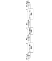
- FIG. 1 is a diagram showing an example of the configuration of a module circuit 1 according to this embodiment.
- a module circuit 1 includes a synapse element circuit 2 , a weight adjustment circuit 4 and a LIF neuron circuit 3 .
- the synapse element circuit 2 , the weight adjustment circuit 4 , and the LIF neuron circuit 3 are connected in series in this order and provided in the module circuit 1 .
- the module circuit 1 is used, for example, as a synapse for a neural network.
- An input pulse signal IP1 is input to the synapse element circuit 2 .
- the input pulse signal IP1 is a pulse signal output from a synapse provided in the front stage of the module circuit 1 .
- the synapse element circuit 2 integrates the inputted input pulse signal IP1 and outputs a pulse signal MP2 as an output pulse signal having a frequency corresponding to the integrated value.
- the synapse element circuit 2 is an example of a first block circuit.
- the weight adjustment circuit 4 adjusts the pulse width of the pulse signal MP2 output from the module circuit 1. The wider the pulse width, the faster the rate of charge and discharge of neurons in the later stages. That is, wide pulse widths correspond to large weights in the neural network.
- the weight adjustment circuit 4 outputs the pulse signal MP2 with the adjusted pulse width as the pulse signal MP3.
- the pulse signal MP3 is output to the LIF neuron circuit 3.
- the weight adjustment circuit 4 is an example of a second block circuit.
- the LIF neuron circuit 3 uses the leak current of the transistor to charge the node.
- the LIF neuron circuit 3 outputs an output pulse signal OP1 and is reset when the voltage of the charged node exceeds the threshold.
- the output pulse signal OP1 is output to the subsequent neuron.
- the pulse signal MP3 input from the weight adjustment circuit 4 increases or decreases the frequency at which the pulse signal is output.
- the LIF neuron circuit 3 is an example of a third block circuit.
- the module circuit 1 is a LIF (Leaky Integration and Fire) element that uses analog quantities (pulse intervals and pulse widths) in the time domain.
- LIF Leaky Integration and Fire
- analog quantities pulse intervals and pulse widths
- an LIF element with lower power consumption than a LIF element based on a conventional analog system (integration circuit) is realized.
- FIG. 2 is a diagram showing an example of the configuration of the synapse element circuit 2 according to this embodiment.
- the synapse element circuit 2 includes an input terminal IN21, an inverter D21, a P-type MOS transistor T21, a power supply terminal P2, an input terminal IN22, an N-type MOS transistor T22, a ring oscillator O2, a capacitor C2, and an N-type It has a MOS transistor T23, an output terminal OUT21, and an output terminal OUT22.
- the P-type MOS transistor T21, the N-type MOS transistor T22, and the N-type MOS transistor T23 are off when no signal is input.
- An input pulse signal IP21 is input to the input terminal IN21.
- the input pulse signal IP21 is a rectangular wave that goes high for a short period of time in a predetermined cycle.
- the input pulse signal IP21 corresponds to the input pulse signal IP1 shown in FIG.
- the input terminal IN21 is an example of a first input terminal.
- the inverter D21 inverts the polarity of the input pulse signal IP21 input to the input terminal IN21.
- the polarity-inverted input pulse signal IP21 is a rectangular wave that goes low for a short period of time in a predetermined cycle.
- the P-type MOS transistor T21 has its source connected to the power supply terminal P2, its gate connected to the inverter D21, and its drain connected to the connection point J22 of the wiring L21.
- the P-type MOS transistor T21 is turned on only while the input pulse signal IP21 whose polarity is inverted by the inverter D21 is low, and the current I21 flows from the source to the drain. As described above, the polarity-inverted input pulse signal IP21 is low for a short period of time, so the P-type MOS transistor T21 is turned on for that short period of time.
- the P-type MOS transistor T21 is an example of a high-side switching element.
- the high-side switching element opens and closes according to an input pulse signal IP21 indicating an excitatory input, thereby forming a pulse voltage that charges the capacitor C2.
- An input pulse signal IP22 is input to the input terminal IN22.
- the input pulse signal IP22 is a rectangular wave that goes high for a short period of time in a predetermined cycle.
- the pulse width of the input pulse signal IP22 is, for example, narrower than the pulse width of the input pulse signal IP21.
- the input pulse signal IP22 corresponds to the input pulse signal IP1 shown in FIG.
- the input terminal IN21 is an example of a first input terminal.
- the N-type MOS transistor T22 has its source connected to the connection point J21 between the capacitor C2 and the wiring L21, its gate connected to the input terminal IN22, and its drain grounded.
- the N-type MOS transistor T22 is turned on only while the input pulse signal IP22 is high, and the current I22 flows from the source to the drain. As described above, the input pulse signal IP22 is high for a short period of time, so the N-type MOS transistor T22 is turned on for that short period of time.
- the N-type MOS transistor T22 is an example of a low-side switching element.
- the low-side switching element discharges the charge of the capacitor C2 by opening and closing in response to an input pulse signal IP22 indicating an inhibitory input.
- the capacitor C2 is provided on the wiring L21. Each time the P-type MOS transistor T21 is turned on for a short period of time and the current I21 flows, the capacitor C2 is charged for that short period of time and charges accumulate in the capacitor C2.
- the capacitance of the capacitor C2 is, for example, 150 fF (femtofarad). The other end of capacitor C2 is grounded.
- the capacitor C2 is an example of a holding unit.
- the holding unit holds an average value of the input pulse signal IP21 for a predetermined period according to the interval of the input pulse signal IP21 and the width of the input pulse signal IP21.
- the holding unit includes a capacitor C2, integrates a pulse voltage indicating the input pulse signal IP21, and holds the result of integrating the pulse voltage as an average value.
- the ring oscillator O2 is an oscillation circuit (oscillator) that outputs a pulse signal.
- Ring oscillator O2 includes three inverters, inverter D22, inverter D23, and inverter D24.
- the inverter D22 is connected to the wiring L21 by a connection point J21.
- the inverter D23 is connected to the wiring L21 by a connection point J22.
- Inverter D24 is connected to line L21 by connection point J23.
- Inverter D22, inverter D23, and inverter D24 are connected in series in this order.
- the inverter D24 is connected in series to the inverter D22 by a wiring L24 via a connection point J26. That is, the ring oscillator O2 has a ring-shaped structure.
- the ring oscillator O2 is an example of an oscillator.
- the oscillation section generates the output pulse signal OP2 at a frequency corresponding to the average value of the input pulse signal IP21 held by the holding section.
- the oscillation section is supplied with an integrated current obtained by integration of the pulse voltage by the holding section from the holding section and generates an output pulse signal OP2 having a frequency dependent on the magnitude of the integrated current.
- the integral current is a current that monotonously increases with respect to the result of integrating the pulse voltage by the holding unit.
- the signal output from the inverter D24 is branched into two at the connection point J26.
- One of the signals branched at the connection point J26 is output to the output terminal OUT22.
- the output terminal OUT22 outputs one of the branched signals as the output pulse signal OP2.
- the output pulse signal OP2 corresponds to the pulse signal MP2 shown in FIG.
- the other of the signals branched at connection point J26 is input to inverter D22 via line L24.
- the inverter D22 When a low signal is input to the inverter D22, the polarity of the signal is inverted by the inverters D22, D23, and D24, and a high signal is output from the inverter D24. Similarly, when a high signal is input to the inverter D22, a low signal is output from the inverter D24. The signal output from the inverter D24 periodically repeats low and high. As a result, the output pulse signal OP2 is output from the inverter D24.
- the pulse interval of the output pulse signal OP2 depends on the node voltage V2.
- the connection point J21, the connection point J22, and the connection point J23 are collectively referred to as nodes.
- the voltage is determined by the voltage on capacitor C2. Therefore, the pulse interval of output pulse signal OP2 depends on the voltage of capacitor C2.
- the input pulse signal IP21 is integrated by the charge accumulated in the capacitor C2, and the output pulse signal OP2 having a frequency (pulse interval) corresponding to the integrated value is output. That is, the waveform of the output pulse signal OP2 corresponds to the result of integrating the waveform of the input pulse signal IP21.
- the waveform of the output pulse signal OP2 is used for learning when the synapse element circuit 2 is used as a node of the neural network.
- the output pulse signal OP2 corresponds to the pulse signal MP2 shown in FIG.
- the ring oscillator O2 consumes current.
- a current consumed by the ring oscillator O2 is called a leak current I23.
- Leakage current I23 flows out from junction J24.
- the value of the node voltage V2 shown in FIG. 2 rises each time the P-type MOS transistor T21 is turned on, and decreases as the ring oscillator O2 operates and the leak current I23 flows out.
- an output pulse signal OP2 is generated by a leakage current I23 that flows out according to the operation of the ring oscillator O2. That is, in the synapse element circuit 2, the leak current is converted into a pulse train.
- the amount of leakage current I23 is adjusted by the N-type MOS transistor T23.
- the N-type MOS transistor T23 has its source connected to the connection point J24, and its drain and gate grounded through the connection point J25.
- N-type MOS transistor T23 is an example of an inflow limiter. The inflow limiter limits the inflow of integral current from the holding section to the oscillation section.
- the N-type MOS transistor T23 may be omitted from the configuration of the synapse element circuit 2. If the N-type MOS transistor T23 is not provided, adjusting only the amount of the current I21 flowing through the P-type MOS transistor T21 cannot adjust the amount of the leak current I23 flowing out of the ring oscillator O2. Therefore, the accuracy of adjustment for making the output pulse signal OP2 output from the ring oscillator O2 into a desired pulse train is higher with the N-type MOS transistor T23 than without it.
- the input terminal IN22 and the N-type MOS transistor T22 may be omitted from the configuration of the synapse element circuit 2.
- FIG. 3 is a diagram showing an example of the configuration of the weight adjustment circuit 4 according to this embodiment.
- the weight adjustment circuit 4 includes an input terminal IN4, an inverter D41, a delay line D42, a multiplexer M4, a gate A4, and an output terminal OUT4.
- An input pulse signal IP4 is input to the input terminal IN4.
- the input pulse signal IP4 corresponds to the pulse signal MP2 shown in FIG. 1 (in other words, the output pulse signal OP2 shown in FIG. 2). That is, the output pulse signal OP2 output from the first block circuit is input to the input terminal IN4.
- the input pulse signal IP4 input to the input terminal IN4 is branched into the pulse signal IP41 and the pulse signal IP42 at the connection point J41.
- Pulse signal IP41 is input to inverter D41.
- Pulse signal IP42 is input to gate A4.
- Inverter D41 inverts the polarity of pulse signal IP41 and outputs it to delay line D42.
- the delay line D42 is composed of a plurality of delay elements connected in series.
- Multiplexer M4 selects one of the plurality of delay elements forming delay line D42 and outputs it as pulse signal IP43.
- the pulse signal IP43 is delayed compared to the pulse signal IP42 depending on which delay element the signal is extracted from. Of the plurality of delay elements connected in series in the delay line D42, the farther the delay element from which the signal is extracted is from the inverter D41 side, the more the extracted pulse signal IP43 is delayed compared to the pulse signal IP42.
- a pulse signal IP42 and a pulse signal IP43 delayed from the pulse signal IP42 are input to the gate A4.
- Gate A4 outputs a signal corresponding to the AND of the input pulse signal IP42 and pulse signal IP43.
- a signal output from the gate A4 is output as an output pulse signal OP4 from the output terminal OUT4.
- the pulse width of the output pulse signal OP4 is narrower than that of the input pulse signal IP4, depending on which delay element in the delay line D42 the signal is extracted from.
- FIG. 3 shows the waveform of the pulse signal IP43, the waveform of the pulse signal IP42, and the waveform of the output pulse signal OP4.
- the waveform of the pulse signal IP42 is the same as that of the input pulse signal IP4 because the pulse signal IP42 is just the input pulse signal IP4 branched at the connection point J41.
- the pulse signal IP43 is delayed with respect to the pulse signal IP42.
- the weight adjusting circuit 4 adjusts the pulse width of the output pulse signal OP4 according to which delay element in the delay line D42 takes out the signal.
- Inverter D41, delay line D42, and multiplexer M4 are one example of a duty ratio adjuster.
- the duty ratio adjuster adjusts the duty ratio of the output pulse signal OP4.
- the output terminal OUT4 is an example of a second output terminal. The second output terminal outputs the output pulse signal OP4 adjusted by the duty ratio adjuster.
- the configuration of the weight adjustment circuit 4 is not limited to the configuration shown in FIG. 3 as long as the pulse duty ratio can be adjusted.
- the configuration of the weight adjustment circuit 4 may be another configuration such as a configuration in which the pulse width is adjusted by varying the load capacitance.
- FIG. 4 is a diagram showing an example of the configuration of the LIF neuron circuit 3 according to this embodiment.
- the LIF neuron circuit 3 includes an input terminal IN31, a P-type MOS transistor T31, an input terminal IN32, an N-type MOS transistor T32, a power supply terminal P31, a capacitor C3, a power supply terminal P32, and a P-type MOS transistor T33.
- a P-type MOS transistor T34, an N-type MOS transistor T35 an inverter D31, an inverter D32, an inverter D33, an inverter D34, and an output terminal OUT3.
- the P-type MOS transistor T31, N-type MOS transistor T32, P-type MOS transistor T33, P-type MOS transistor T34, and N-type MOS transistor T35 are off when no signal is input. Also, the parasitic capacitance of each of the P-type MOS transistor T31, N-type MOS transistor T32, P-type MOS transistor T33, P-type MOS transistor T34, and N-type MOS transistor T35 is, for example, 10 fF (femtofarad).
- the P-type MOS transistor T33 has a source connected to the power supply terminal P32, a gate connected to the connection point J35, and a drain connected to the source of the P-type MOS transistor T34.
- the P-type MOS transistor T34 has its source connected to the drain of the P-type MOS transistor T33, its gate connected to the connection point J34, and its drain connected to the connection point J33.
- the P-type MOS transistor T33 and the P-type MOS transistor T34 are off.
- a leak current I31 flows through the P-type MOS transistor T33 and the P-type MOS transistor T34 even in the off state.
- Leakage current I31 always flows even in the off state.
- the capacitor C3 is connected to the connection point J33 via the connection point J32.
- the leakage current I31 flows through the P-type MOS transistors T33 and T34, charges accumulate in the capacitor C3. Therefore, in the LIF neuron circuit 3, the capacitor C3 is charged by the leakage current I31 flowing through the P-type MOS transistors T33 and T34. That is, the capacitor C3 is charged by the leak current I31 of the P-type MOS transistor T33 and the P-type MOS transistor T34, which are MOS transistors.
- Capacitor C3 is included in the charging section.
- the CMOS inverter P-type MOS transistor T33 and N-type MOS transistor T35.
- Inverter D32, inverter D33, and inverter D34 are provided in series in this order.
- the inverter D32 is connected to the connection point J34, and the inverter D34 is connected to the connection point J35.
- a signal output from the inverter D31 is inverted by three inverters, an inverter D32, an inverter D33, and an inverter D34, and output from the inverter D34.
- the pulse signal output from the inverter D34 is output as the output pulse signal OP3 from the output terminal OUT3 to the connection point J35.
- the output pulse signal OP3 corresponds to the output pulse signal OP1 shown in FIG.
- the N-type MOS transistor T35 has its source connected to the connection point J33, its gate connected to the connection point J35, and its drain grounded.
- the output pulse signal OP3 output from the inverter D34 goes high for a short period of time
- the N-type MOS transistor T35 is turned on for that short period of time.
- the charge stored in the capacitor C3 flows out, and a current I32 flows through the N-type MOS transistor T35 from the source to the drain.
- the voltage of the capacitor C3 is reset by the current I32 flowing through the N-type MOS transistor T35.
- connection point J31, the connection point J32, and the connection point J33 are collectively referred to as nodes. Therefore, voltage V3 is the voltage of the node.
- the value of the voltage V3 of the node shown in FIG. 4 rises due to accumulation of charge due to leakage current I31 of the P-type MOS transistors T33 and T34.
- the way in which the value of the voltage V3 rises due to the leak current I31 is an upwardly convex, moderately increasing function when the value is expressed as a function of time.
- the voltage V3 rises sharply.
- the signal output from the inverter D31 is inverted by the three inverters D32, D33, and D34, and delayed by the required time to turn on the N-type MOS transistor T35.
- the N-type MOS transistor T35 is turned on, the capacitor C3 is reset and the value of the voltage V3 rapidly decreases.
- a peak is formed in the time change of the voltage V3 due to the rapid rise of the voltage V3 due to the voltage V3 of the node exceeding the threshold of the inverter D31 and the rapid decrease of the voltage V3 due to the resetting of the capacitor C3. be.
- the time when the output pulse signal OP3 goes high corresponds to the peak of the time change of the node voltage V3.
- the P-type MOS transistor T33 and the N-type MOS transistor T35 are connected in series between the power supply terminal and the ground terminal.
- the P-type MOS transistor T33 and the N-type MOS transistor T35 are provided as a CMOS inverter.
- the inverter D31 generates an inverted signal by inverting the output from the CMOS inverter. Inverter D31 is an example of an inverter.
- the P-type MOS transistor T34 is arranged between the P-type MOS transistor T33 and the N-type MOS transistor T35 and opens and closes according to the inverted signal generated by the inverter D31.
- the P-type MOS transistor T34 is an example of a switching element.
- the inverter D32, inverter D33, and inverter D34 delay the output from the CMOS inverter (P-type MOS transistor T33 and N-type MOS transistor T35) and input it to the CMOS inverter again.
- the inverter D32, the inverter D33, and the inverter D34 are examples of delay circuits.
- the inverter D31, the P-type MOS transistor T34, the inverter D32, the inverter D33, and the inverter D34 are included in the pulse signal generation section.
- the pulse signal generator includes an inverter (inverter D31), a switching element (P-type MOS transistor T34), and a delay circuit (inverter D32, inverter D33, and inverter D34).
- the pulse signal generating section generates a pulse signal and resets the charging amount of the charging section when the charging amount of the charging section exceeds the threshold.
- the output terminal OUT3 is an example of a third output terminal.
- the third output terminal outputs the output pulse signal OP3 generated by the pulse signal generator.
- the output pulse signal OP3 corresponds to the output pulse signal OP1 shown in FIG. 1, and is output to the subsequent neuron.
- the P-type MOS transistor T31 and N-type MOS transistor T32 adjust the pulse interval of the output pulse signal OP3.
- the adjustment of the pulse interval of the output pulse signal OP3 by the P-type MOS transistor T31 and the N-type MOS transistor T32 will be described below.
- An input pulse signal IP31 is input to the input terminal IN31.
- the input pulse signal IP31 is a rectangular wave that goes low for a short period of time in a predetermined cycle.
- the input terminal IN31 is an example of a third input terminal to which the output pulse signal OP4 (in other words, the pulse signal MP3 shown in FIG. 1) output from the second block circuit (weight adjustment circuit 4) is input.
- the P-type MOS transistor T31 has a source connected to the power supply terminal P31, a gate connected to the input terminal IN31, and a drain connected to the connection point J31.
- the P-type MOS transistor T31 When the input pulse signal IP31 input to the gate of the P-type MOS transistor T31 becomes low for a short period of time, the P-type MOS transistor T31 is turned on for a short period of time.
- a current I33 flows through the P-type MOS transistor T31 from the source to the drain. Due to the current I33 flowing through the P-type MOS transistor T31, charges are accumulated in the capacitor C3.
- the capacitor C3 is also charged by the leakage current I31 flowing through the P-type MOS transistors T33 and T34. Therefore, by turning on the P-type MOS transistor T31, more electric charge is accumulated in the capacitor C3 than when the P-type MOS transistor T31 is turned off.
- An input pulse signal IP32 is input to the input terminal IN32.
- the input pulse signal IP32 is a rectangular wave that goes high for a short period of time in a predetermined cycle.
- the input terminal IN32 is an example of a third input terminal to which the output pulse signal OP1 output from the second block circuit (weight adjustment circuit 4) is input.
- the N-type MOS transistor T32 has a source connected to the connection point J31, a gate connected to the input terminal IN32, and a drain grounded.
- the N-type MOS transistor T32 is turned on for a short period of time when the input pulse signal IP32 input to its gate becomes high for a short period of time.
- a current I34 flows through the N-type MOS transistor T32 from the source to the drain.
- a current I34 flows through the N-type MOS transistor T32, whereby charges flow out from the capacitor C3. Therefore, by turning on the N-type MOS transistor T32, less charge is accumulated in the capacitor C3 than when the N-type MOS transistor T32 is turned off.
- the N-type MOS transistor T32 discharges the charge of the input pulse signal IP32 in the closed state by opening and closing in response to the input pulse signal IP32 indicating the suppressive input.
- the N-type MOS transistor T32 is an example of a second low-side switching element.
- the input pulse signal IP32 is an example of a second input pulse signal.
- the P-type MOS transistor T31 generates a pulse voltage indicating the input pulse signal IP31 by opening and closing according to the input pulse signal IP31 indicating an excitatory input.
- the P-type MOS transistor T31 is an example of a second high side switching element.
- the input pulse signal IP31 is an example of a first input pulse signal.
- the input of the pulse signal to the P-type MOS transistor T31 or the N-type MOS transistor T32 increases or decreases the charge accumulated in the capacitor C3.
- the node voltage V3 changes as the charge accumulated in the capacitor C3 increases or decreases.
- the output pulse signal OP3 output from the output terminal OUT3 becomes high when the voltage V3 exceeds the threshold of the inverter D31.
- the pulse interval of the output pulse signal OP3 can be adjusted by the input pulse signal IP31 or the input pulse signal IP32.
- the LIF neuron circuit 3 can increase or decrease the output frequency of the output pulse signal OP3 according to the input pulse signal IP31 or the input pulse signal IP32.
- the input pulse signal IP31 corresponds to an excitatory pulse.
- the input pulse signal IP32 corresponds to an inhibitory pulse.
- the capacitor C3 is charged with a pulse voltage indicating the input pulse signal (input pulse signal IP31 or input pulse signal IP32).
- Capacitor C3 is a second capacitor charged by a pulse voltage indicating output pulse signal OP4 (that is, input pulse signal IP31 or input pulse signal IP32) input to the third input terminal (input terminal IN31 or input terminal IN32).
- a pulse voltage indicating output pulse signal OP4 that is, input pulse signal IP31 or input pulse signal IP32
- the input pulse signal IP31 or the input pulse signal IP32 is the output pulse signal OP4 output from the weight adjustment circuit 4 provided in the preceding stage of the LIF neuron circuit 3.
- the input pulse signal IP31 is input from one weight adjustment circuit 4
- the input pulse signal IP32 is input from the other weight adjustment circuit 4.
- a synapse element circuit 2 is provided in the preceding stage of each weight adjustment circuit 4 .
- the frequency with which the pulse signal generator generates the output pulse signal OP3 is the frequency with which the output pulse signal OP4 output from the weight adjustment circuit 4 is input to the third input terminal (input terminal IN31 or input terminal IN32). increase or decrease accordingly.
- Either one of the P-type MOS transistor T31 or the N-type MOS transistor T32 may be omitted from the configuration of the LIF neuron circuit 3. For example, if the LIF neuron circuit 3 only shortens the pulse interval, it is sufficient to provide the P-type MOS transistor T31. On the other hand, if the LIF neuron circuit 3 only lengthens the pulse interval, it is sufficient to provide the N-type MOS transistor T32.
- the pulse interval of the output pulse signal OP3 is determined by the transistors provided in the LIF neuron circuit 3 (P-type MOS transistor T31, N-type MOS transistor T32, P-type MOS transistor T33, P-type MOS transistor T34, and N-type MOS transistor T35). ) also depends on the size of Therefore, by adjusting the size of the transistors provided in the LIF neuron circuit 3, the pulse interval of the output pulse signal OP3 output from the LIF neuron circuit 3 can be adjusted. However, since the transistor size is determined at the time the LIF neuron circuit 3 is assembled, the adjustment of the pulse interval according to the transistor size is an adjustment made at the time the LIF neuron circuit 3 is assembled.
- the magnitude of the leak current I31 is much smaller than the magnitude of the current I33 flowing through the P-type MOS transistor T31 or the magnitude of the current I34 flowing through the N-type MOS transistor T32.
- Leakage current also flows through the P-type MOS transistor T31 and the N-type MOS transistor T32 even in the off state.
- the charge accumulated in the capacitor C3 also increases or decreases depending on leakage currents flowing through the P-type MOS transistor T31 and the N-type MOS transistor T32. Due to the leakage current flowing through the P-type MOS transistor T31, electric charges are accumulated in the capacitor C3. Electric charge flows out from the capacitor C3 due to the leakage current flowing through the N-type MOS transistor T32.
- the module circuit 1 has the pulse interval of the input pulse signal (input pulse signal IP1 shown in FIG. 1) and the pulse interval of the output pulse signal (output pulse signal OP1 shown in FIG. 1). The relationship becomes a non-linear relationship.
- the LIF neuron circuit 3 may be omitted from the configuration of the module circuit 1. In that case, the output pulse signal OP2 output from the synapse element circuit 2 is directly input to the input terminal IN4, which is the second input terminal.
- the configuration of the low-side switching element may be omitted from the configuration of the synapse element circuit 2 .
- the input pulse signal IP22 indicating an inhibitory input can be input to the synapse element circuit 2 . Therefore, in the synapse element circuit 2 having the configuration of the low-side switching elements, even if the LIF neuron circuit 3 is omitted from the configuration of the module circuit 1, the frequency and width of pulses input to the synapse element circuit 2 are large. It is possible to reduce the frequency of output pulses as the number increases.
- the LIF neuron circuit 3 has the function of stabilizing the operation of the neural network.
- FIG. 5 is a diagram showing an example of the configuration of the reservoir circuit N1 according to this embodiment.
- the reservoir circuit N1 consists of three layers, an input layer, an intermediate layer, and an output layer, for example.
- the input layer includes a LIF element M11, a LIF element M12, a LIF element M13, and a LIF element M14.
- the intermediate layer includes a LIF element M21, a LIF element M22, and a LIF element M23.
- the output layer includes a LIF element M31, a LIF element M32, a LIF element M33, and a LIF element M34.
- Each of these LIF elements (LIF element M11, LIF element M12, . . . , LIF element M34) has the same configuration as the module circuit 1 shown in FIG. That is, the reservoir circuit N1 is a reservoir circuit including a plurality of module circuits 1.
- FIG. 1 is a reservoir circuit including a plurality of module circuits 1.
- An output terminal OUT3 (FIG. 4) provided in the LIF element M11 is connected to an input terminal IN21 or an input terminal IN22 (FIG. 2) provided in the LIF element M21.
- An output terminal OUT3 (FIG. 4) provided in the LIF element M12 is connected to an input terminal IN21 or IN22 (FIG. 2) provided in the LIF element M21.
- the output pulse signal OP3 output from each of the LIF element M11 and the LIF element M12 is input to the LIF element M21 as the input pulse signal IP21 or the input pulse signal IP22. Therefore, the output terminal OUT3 provided in each of the one or more module circuits 1 and the input terminal IN21 or the input terminal IN22 provided in one module circuit 1 are connected.
- An output terminal OUT3 (FIG. 4) provided in the LIF element M12 is connected to an input terminal IN21 or IN22 (FIG. 2) provided in the LIF element M21.
- An output terminal OUT3 (FIG. 4) provided in the LIF element M12 is connected to an input terminal IN21 or IN22 (FIG. 2) provided in the LIF element M22.
- the output pulse signal OP3 output from the LIF element M12 is input to the LIF element M21 and the LIF element M22 as the input pulse signal IP21 or the input pulse signal IP22. Therefore, the output terminal OUT3 provided in one module circuit 1 and the input terminal IN21 or the input terminal IN22 provided in each of the one or more module circuits 1 are connected.
- FIG. 6 is a diagram showing an example of operation confirmation results when one synapse element circuit, one weight adjustment circuit, and one LIF neuron circuit are connected according to the present embodiment.
- a plurality of graphs shown in FIG. 6 show time variations of each value of weight setting, excitatory pulse, intraneuronal integration terminal, neuron output pulse, intrasynaptic integration output, integration result readout, and synapse output signal.
- the operation confirmation result shown in FIG. 6 only the excitatory pulse is input to the LIF neuron circuit 3, and the inhibitory pulse is not input.
- the weight setting indicates duty ratio setting data for the weight adjustment circuit 4 .
- the value of the signal that instructs the multiplexer M4 (FIG. 3) provided in the weight adjustment circuit 4 to select which of the plurality of delay elements forming the delay line D42 as the delay element for extracting the pulse signal is set to: show.
- the excitatory pulse indicates the value of the input pulse signal IP4 input to the input terminal IN4 provided in the weight adjustment circuit 4.
- FIG. An excitatory pulse is a pulse signal generated with a constant period, amplitude and duty ratio.
- the intra-neuron integration terminal indicates the value of the voltage V3 of the nodes provided in the LIF neuron circuit 3 (connection point J31, connection point J32, and connection point J33).
- the value of node voltage V3 is equal to the value of the voltage on capacitor C3 as described above.
- the neuron output pulse indicates the value of the output pulse signal OP3 output from the output terminal OUT3 provided in the LIF neuron circuit 3.
- the intra-synapse integration output indicates the value of the voltage V2 at the nodes provided in the synapse element circuit 2 (connection point J21, connection point J22, and connection point J23).
- the value of node voltage V2 is equal to the value of the voltage on capacitor C2 as described above.
- the integration result read indicates the value of the signal output from the output terminal OUT21 provided in the synapse element circuit 2.
- FIG. The synapse output signal indicates the value of the output pulse signal OP2 output from the output terminal OUT22 provided in the synapse element circuit 2.
- the synapse element circuit 2 functions as an LIF element from the time change of the intra-synapse integration output or the integration result readout.
- the average power consumption in the LIF neuron circuit 3 was 2.5 nW (nanowatts).
- the average power consumption in the synapse element circuit 2 was 3.0 nW.
- FIG. 7 is a diagram showing an example of operation confirmation results when one synapse element circuit, one weight adjustment circuit, and one LIF neuron circuit according to the present embodiment are connected.
- a plurality of graphs shown in FIG. 7 show temporal changes in each value of an excitatory pulse, an inhibitory pulse, an intra-synaptic integration output, an integration result readout, a synaptic output signal, an intra-neuron integration terminal, and a neuron output pulse.
- the LIF neuron circuit 3 receives an excitatory pulse and an inhibitory pulse.
- the excitatory pulse indicates the value of the input pulse signal IP31 input to the input terminal IN4 provided in the weight adjustment circuit 4.
- FIG. An excitatory pulse is a pulse signal generated with a constant period, amplitude and duty ratio.
- the inhibitory pulse indicates the value of the input pulse signal IP32 input to the input terminal IN32 provided in the weight adjustment circuit 4.
- FIG. An inhibitory pulse is a pulse signal generated with a constant period, amplitude, and duty ratio.
- the neuron output pulse is always low during the period when the inhibitory pulse is input.
- the pulse interval of the neuron output pulse is short in the period in which the pulse interval of the excitatory pulse is short. That is, as described above, in the LIF neuron circuit 3, the output frequency of the output pulse signal OP3 can be increased or decreased by the input pulse signal IP31, which is an excitatory pulse, or the input pulse signal IP32, which is an inhibitory pulse.
- FIG. 8 is a diagram showing an example of the operation check result of the spiking NN according to this embodiment.
- the spiking NN is composed of four module circuits 1, for example.
- a plurality of graphs shown in FIG. 8 show temporal changes in values of spike output, integration output, and VCO (Voltage-controlled oscillator) output.
- a plurality of graphs shown in FIG. 8 show respective values of the spike output, integration output, and VCO output for each of the four module circuits 1.
- the spike output indicates the value of the output pulse signal OP3 output from the output terminal OUT3 provided in the LIF neuron circuit 3.
- FIG. The integrated output indicates the value of the voltage V2 at the nodes (connection point J21, connection point J22, and connection point J23) provided in the synapse element circuit 2.
- the VCO output indicates the value of the output pulse signal OP2 output from the output terminal OUT22 provided in the synapse element circuit 2.
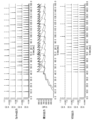
- FIG. 9 is a diagram showing an example of temporal changes in synapse output signals according to the present embodiment.
- the synapse output signal indicates the value of the output pulse signal OP2 output from the output terminal OUT21 provided in the synapse element circuit 2.
- FIG. 9 is a diagram showing an example of temporal changes in synapse output signals according to the present embodiment.
- the synapse output signal indicates the value of the output pulse signal OP2 output from the output terminal OUT21 provided in the synapse element circuit 2.
- the teacher signal is shown together with the synapse output signal.
- the teacher signal is a signal for learning that makes the value of the synapse output signal close to the value of the teacher signal.
- the teacher signal is input during the period from the time indicated as "RLS on” to the time indicated as "off” in FIG.
- the graph of the synapse output signal almost overlaps the graph of the teacher signal during the period when the teacher signal is being input.
- the graph of the synapse output signal shows the same temporal change as the period during which the teacher signal is input in the period after the input of the teacher signal (the period after the time indicated as "off"). That is, the graph of the synapse output signal changes with the teacher signal so as to change over time in the same way as the graph of the teacher signal. In other words, it can be seen that learning can be realized by the spiking NN composed of the module circuit 1.
- FIG. 10 is a diagram showing an example of temporal changes in neuron voltage according to this embodiment.
- the neuron voltage indicates the value of the voltage V3 of the nodes (connection point J31, connection point J32, and connection point J33) provided in the LIF neuron circuit 3, similar to the intra-neuron integration terminals (FIGS. 6 and 7) described above. .
- FIG. 11 is a diagram showing an example of temporal changes in synaptic currents according to this embodiment.
- the synapse current indicates the value of the voltage V2 at the nodes (connection point J21, connection point J22, and connection point J23) provided in the synapse element circuit 2, similar to the above-described intrasynaptic integral output (FIGS. 6 and 7). .
- the module circuit 1 includes a first block circuit (the synapse element circuit 2 in the present embodiment) and a second block circuit (the weight adjustment circuit 4 in the present embodiment). , provided.
- the first block circuit (synapse element circuit 2 in this embodiment) includes a first input terminal (input terminal IN21 in this embodiment), a holding section (capacitor C2 in this embodiment), an oscillation section (this In the embodiment, it includes a ring oscillator O2) and a first output terminal (output terminal OUT22 in the embodiment).
- the input pulse signal IP1 is input to the first input terminal (input terminal IN21 in this embodiment).
- the holding unit holds the average value of the input pulse signal IP1 for a predetermined period according to the interval of the input pulse signal IP1 and the width of the input pulse signal IP1.
- the oscillator (ring oscillator O2 in this embodiment) generates the output pulse signal OP2 at a frequency corresponding to the average value.
- the first output terminal (output terminal OUT22 in this embodiment) outputs an output pulse signal OP2.
- the second block circuit (weight adjustment circuit 4 in this embodiment) includes a second input terminal (input terminal IN4 in this embodiment) and a duty ratio adjuster (inverter D41, delay line D42, and multiplexer M4), and a second output terminal (output terminal OUT4 in this embodiment).
- the second input terminal receives the output pulse signal OP2 output from the first block circuit (synapse element circuit 2 in this embodiment).
- a duty ratio adjuster (in this embodiment, an inverter D41, a delay line D42, and a multiplexer M4) adjusts the duty ratio of the output pulse signal OP2.
- the second output terminal (output terminal OUT4 in this embodiment) outputs an output pulse signal (in this embodiment, It outputs an output pulse signal OP4).
- the output pulse signal can be output at a frequency corresponding to the time domain information such as the interval of the input pulse signal and the width of the pulse signal. realizable.
- the module circuit 1 according to the present embodiment relates to a low power consumption integrated circuit mounting system for neuron elements used in neural networks and the like.
- the module circuit 1 according to the present embodiment does not use voltage or current as information, but uses time-domain information such as the period and pulse width of binary pulse signals of low and high. Enables heat generation and high integration.
- the module circuit 1 according to the present embodiment can operate with extremely low power consumption because it operates mainly by utilizing the leak current flowing through the transistor in the off state.
- the module circuit 1 according to the present embodiment can operate with low power consumption, does not require a large capacity, and can realize a time constant in milliseconds with a relatively small area.
- the module circuit 1 adjusts the transition time between binary voltages of 0 or 1 without precisely controlling analog quantities that are sensitive to noise and the like. do. Therefore, it is easy to implement even in a low-voltage process technology, has a high affinity for advanced processes, and has the advantage of being able to increase the degree of integration.
- the enlarged area R2 is an enlarged area of the rectangular area R1 of the semiconductor chip.
- the enlarged region R2 has a long side length of 70 ⁇ m and a short side length of 30 ⁇ m.
- the area of the semiconductor chip of the LIF neuron circuit is 127 mm 2 .
- the area of the semiconductor chip of the synapse element circuit is 231 mm 2 .
- the area of the semiconductor chip of the weight adjustment circuit is 525 mm 2 .
- the configuration of the synapse element circuit 20 is the same as the configuration of the synapse element circuit 2 (FIG. 2) according to the embodiment described above.
- the configuration of the weight adjustment circuit 40 is the same as the configuration of the weight adjustment circuit 4 (FIG. 3) according to the embodiment described above.
- the configuration of the LIF neuron circuit 30 is the same as the configuration of the LIF neuron circuit 3 (FIG. 4) according to the embodiment described above. Therefore, in the examples described below, the respective symbols used in the above-described embodiments may be used for description.
- FIG. 13 is a diagram showing an example of the configuration of the module circuit 10a according to this embodiment.
- the module circuit 10 a includes a pulse generator 50 , a weight adjustment circuit 40 and a LIF neuron circuit 30 .
- the pulse generator 50, the weight adjustment circuit 40, and the LIF neuron circuit 30 are connected in series in this order and provided in the module circuit 10a.
- the pulse generator 50 generates a rectangular wave of 100 Hz as the input pulse signal IP4.
- An input pulse signal IP4 generated by the pulse generator 50 is input to the input terminal IN4 of the weight adjustment circuit 40.
- FIG. When the input pulse signal IP4 is input to the input terminal IN4, the output pulse signal OP4 is output from the output terminal OUT4 of the weight adjustment circuit 40.
- FIG. An output pulse signal OP4 output from the weight adjustment circuit 40 is input to the input terminal IN31 of the LIF neuron circuit 30.
- FIG. A spike signal V spike is output from an output terminal OUT3 of the LIF neuron circuit 30 as an output pulse signal OP3.
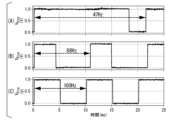
- FIG. 14 shows the waveform of the spike signal V spike output from the module circuit 10a as the operation measurement result of the module circuit 10a.
- 14(A), 14(B), 14(C), and 14(D) the weight values for adjusting the pulse width of the output pulse signal OP4 by the weight adjusting circuit 40 are 1 and 1, respectively.
- 2 shows the waveform of the spike signal V spike for 2, 4, and 8; As shown in FIG. 14, it was confirmed that the larger the weight, the shorter the spike period of the spike signal V spike .
- FIG. 15 is a diagram showing an example of the configuration of the module circuit 10b according to this embodiment.
- the module circuit 10 b includes a pulse generator 51 , a pulse generator 52 , a weight adjustment circuit 41 , a weight adjustment circuit 42 and a LIF neuron circuit 30 .
- the pulse generator 51 and weight adjustment circuit 41 are connected in series in this order.
- the pulse generator 52 and weight adjustment circuit 42 are connected in series in this order.
- a series-connected pulse generator 51 and weight adjustment circuit 41 and a series-connected pulse generator 52 and weight adjustment circuit 42 are connected in parallel to the LIF neuron circuit 30 .
- each of the weight adjustment circuit 41 and the weight adjustment circuit 42 is the same as the configuration of the weight adjustment circuit 40 .
- the configuration of each of the pulse generator 51 and the pulse generator 52 is the same as that of the pulse generator 50 .
- An input pulse signal IP4 which is a rectangular wave of 100 Hz generated by the pulse generator 51, is input to the input terminal IN4 of the weight adjustment circuit 41, and output from the output terminal OUT4 of the weight adjustment circuit 41 as an output pulse signal OP4.
- the input pulse signal IP4 which is a rectangular wave of 100 Hz generated by the pulse generator 52, is input to the input terminal IN4 of the weight adjustment circuit 42, and is output from the output terminal OUT4 of the weight adjustment circuit 42 as the output pulse signal OP4.
- An output pulse signal OP4 output from the weight adjustment circuit 41 is input to an input terminal IN31 of the LIF neuron circuit 30 as an input pulse signal IP31, which is an excitatory pulse.
- the output pulse signal OP4 output from the weight adjustment circuit 42 is input to the input terminal IN32 of the LIF neuron circuit 30 as the input pulse signal IP32, which is an inhibitory pulse.
- a spike signal V spike is output from an output terminal OUT3 of the LIF neuron circuit 30 as an output pulse signal OP3.
- FIG. 16 shows the waveform of the spike signal V spike output from the module circuit 10b as the operation measurement result of the module circuit 10b.
- FIG. 16A shows the waveform of the spike signal V spike when no signal is input to the input terminal IN31 and an inhibitory pulse (input pulse signal IP32) is input to the input terminal IN32.
- FIG. 16B shows the waveform of the spike signal V spike when no signal is input to either the input terminal IN31 or the input terminal IN32.
- FIG. 16C shows the waveform of the spike signal V spike when an excitatory pulse (input pulse signal IP31) is input to the input terminal IN31 and no signal is input to the input terminal IN32. As shown in FIG.
- the LIF neuron circuit 30 periodically outputs the spike signal V spike to the output terminal OUT3 even if no signal is input.
- the period of the spike signal V spike becomes longer.
- FIG. 16(C) when an excitatory pulse is input from the input terminal IN31, the cycle of the spike signal V spike is shortened.
- FIG. 17 is a diagram showing an example of the configuration of the module circuit 10c according to this embodiment. Comparing the configuration of the module circuit 10c and the configuration of the module circuit 10b (FIG. 15) according to the second embodiment, the synapse element circuit 20 is different. In the module circuit 10c, the LIF neuron circuit 30 and the synapse element circuit 20 are connected in series.
- a spike signal V spike output from the output terminal OUT3 of the LIF neuron circuit 30 is input to the input terminal IN22 of the synapse element circuit 20 .
- the pulse signal V ring generated by the ring oscillator O2 is output as the output pulse signal OP2.
- FIG. 18 shows the waveform of the pulse signal V ring output from the module circuit 10c as the operation measurement result of the module circuit 10c.
- FIG. 18A shows the waveform of the pulse signal V ring when no signal is input to the input terminal IN31 and an inhibitory pulse (input pulse signal IP32) is input to the input terminal IN32.
- FIG. 16B shows the waveform of the pulse signal Vring when no signal is input to either the input terminal IN31 or the input terminal IN32.
- FIG. 16(C) shows the waveform of the pulse signal Vring when an excitatory pulse (input pulse signal IP31) is input to the input terminal IN31 and no signal is input to the input terminal IN32. As shown in FIG.
- the synapse element circuit 20 periodically outputs a square wave as the pulse signal V ring in response to the spike signal V spike output from the LIF neuron circuit 30 .
- the frequency of the rectangular wave is reduced.
- the frequency of the rectangular wave increases.
- FIG. 19 is a diagram showing an example of the configuration of the module circuit 10d according to this embodiment.
- the module circuit 10 d includes a pulse generator 50 , a weight adjustment circuit 40 and a synapse element circuit 20 .
- the pulse generator 50, the weight adjustment circuit 40, and the synapse element circuit 20 are connected in series in this order and provided in the module circuit 10d.
- the pulse generator 50 generates a rectangular wave of 10 Hz as the input pulse signal IP4.
- An input pulse signal IP4 generated by the pulse generator 50 is input to the input terminal IN4 of the weight adjustment circuit 40.
- FIG. When the input pulse signal IP4 is input to the input terminal IN4, the output pulse signal OP4 is output from the output terminal OUT4 of the weight adjustment circuit 40.
- FIG. The output pulse signal OP4 output from the weight adjustment circuit 40 is input to the input terminal IN22 of the synapse element circuit 20.
- the output terminal OUT22 of the synapse element circuit 20 outputs the pulse signal V ring .
- FIG. 20 shows the waveform of the synapse potential signal V SYN and the waveform of the pulse signal V ring output from the module circuit 10d as the operation measurement results of the module circuit 10d.
- FIG. 20A shows the waveform of the synaptic potential signal V SYN .
- FIG. 20B shows the waveform of the pulse signal Vring .
- the pulse signal V ring is output as a rectangular wave whose frequency is modulated according to the voltage of the synapse potential signal V SYN .
- the synapse potential signal V SYN increases in response to the input to the input terminal IN22, the frequency of the pulse signal V ring increases.
- the synapse potential signal V SYN decreases and the frequency of the pulse signal V ring decreases.
- module circuit 2 synapse element circuit 4 weight adjustment circuit IN2 input terminal C2 capacitor O2 ring oscillator OUT22 output terminal IN4 input terminal D41 inverter D42 delay line M4...multiplexer, OUT4...output terminal, IP1...input pulse signal, OP2, OP4...output pulse signal
Abstract
A module circuit comprises a first block circuit and a second block circuit. The first block circuit is provided with a first input terminal to which an input pulse signal is inputted, a holding unit that holds an average value of the input pulse signal for a predetermined period in accordance with the interval of the input pulse signal and the width of the input pulse signal, an oscillator that generates an output pulse signal at a frequency according to the average value, and a first output terminal that outputs the output pulse signal. The second block circuit is provided with a second input terminal to which the output pulse signal outputted from the first block circuit is inputted, a duty ratio adjuster that adjusts the duty ratio of the output pulse signal, and a second output terminal that outputs the output pulse signal adjusted by the duty ratio adjuster.
Description
本発明は、モジュール回路、及びレザバー回路に関する。
本願は、2021年12月7日に、日本に出願された特願2021-198579号に基づき優先権を主張し、その内容をここに援用する。 The present invention relates to module circuits and reservoir circuits.
This application claims priority based on Japanese Patent Application No. 2021-198579 filed in Japan on December 7, 2021, the content of which is incorporated herein.
アナログ方式(積分回路)によるLIF(Leaky Integration and Fire)素子が知られている(特許文献1)。
A LIF (Leaky Integration and Fire) element based on an analog method (integration circuit) is known (Patent Document 1).
しかしながら、特許文献1に記載されるようなアナログ方式によるLIF素子では、消費電力が大きくなる傾向があった。LIF素子において低消費電力を実現できることが求められている。
However, the analog LIF element as described in Patent Document 1 tends to consume a large amount of power. There is a demand for low power consumption in LIF elements.
本発明は上記の点に鑑みてなされたものであり、LIF素子において低消費電力を実現できるモジュール回路、及びレザバー回路を提供する。
The present invention has been made in view of the above points, and provides a module circuit and a reservoir circuit that can achieve low power consumption in LIF elements.
本発明は上記の課題を解決するためになされたものであり、本発明の一態様は、第1ブロック回路と、第2ブロック回路と、を備え、前記第1ブロック回路は、入力パルス信号が入力される第1入力端子と、前記入力パルス信号の間隔、及び前記入力パルス信号の幅に応じて所定期間の前記入力パルス信号の平均値を保持する保持部と、前記平均値に応じた頻度において出力パルス信号を生成する発振部と、前記出力パルス信号を出力する第1出力端子と、を備え、前記第2ブロック回路は、前記第1ブロック回路から出力される前記出力パルス信号が入力される第2入力端子と、前記出力パルス信号のデューティ比を調整するデューティ比調整器と、前記デューティ比調整器によって調整された前記出力パルス信号を出力する第2出力端子と、を備えるモジュール回路である。
The present invention has been made to solve the above problems, and one aspect of the present invention includes a first block circuit and a second block circuit, wherein the first block circuit receives an input pulse signal a first input terminal for input, a holding unit for holding an average value of the input pulse signal for a predetermined period according to the interval of the input pulse signal and the width of the input pulse signal, and a frequency according to the average value. and a first output terminal for outputting the output pulse signal, and the second block circuit receives the output pulse signal output from the first block circuit. a second input terminal, a duty ratio adjuster for adjusting the duty ratio of the output pulse signal, and a second output terminal for outputting the output pulse signal adjusted by the duty ratio adjuster. be.
また、本発明の一態様は、上記のモジュール回路において、前記第1ブロック回路は、前記保持部は、キャパシタを含み、前記入力パルス信号を示すパルス電圧を積分し、前記パルス電圧を積分した結果を前記平均値として保持し、前記発振部は、前記保持部による前記パルス電圧の積分によって得られる、前記パルス電圧を積分した結果に対して単調に増加する積分電流が前記保持部から供給され、前記積分電流の大きさに依存する周波数をもつ前記出力パルス信号を生成し、興奮性の入力を示す前記入力パルス信号に応じて開閉することにより、前記キャパシタにチャージされる前記パルス電圧を形成するハイサイドスイッチング素子と、を備える。
In one aspect of the present invention, in the module circuit described above, the first block circuit includes a capacitor, the holding unit integrates a pulse voltage indicating the input pulse signal, and integrates a result of integrating the pulse voltage. is held as the average value, and the oscillation unit is supplied with an integrated current obtained by integration of the pulse voltage by the holding unit and monotonically increasing with respect to the result of integration of the pulse voltage from the holding unit, generating said output pulse signal with a frequency dependent on the magnitude of said integrated current and opening and closing in response to said input pulse signal indicative of an excitatory input to form said pulse voltage charged to said capacitor; and a high side switching element.
また、本発明の一態様は、上記のモジュール回路において、前記第1ブロック回路は、抑制性の入力を示す前記入力パルス信号に応じて開閉することにより、前記キャパシタの電荷をディスチャージさせるローサイドスイッチング素子をさらに備える。
Further, according to one aspect of the present invention, in the module circuit described above, the first block circuit is a low-side switching element that discharges the charge of the capacitor by opening and closing in response to the input pulse signal indicating a suppressive input. further provide.
また、本発明の一態様は、上記のモジュール回路において、前記第1ブロック回路は、前記保持部から前記発振部への前記積分電流の流入を制限する流入制限器をさらに備える。
In one aspect of the present invention, in the module circuit described above, the first block circuit further includes an inflow limiter that limits inflow of the integration current from the holding unit to the oscillation unit.
また、本発明の一態様は、上記のモジュール回路において、第3ブロック回路をさらに備え、前記第3ブロック回路は、前記第2ブロック回路から出力される前記出力パルス信号が入力される第3入力端子と、MOSトランジスタのリーク電流によって充電される充電部と、前記充電部の充電量が閾値を超えると、パルス信号を生成し、かつ前記充電部の充電量をリセットするパルス信号生成部と、前記パルス信号生成部が生成した前記パルス信号を出力する第3出力端子と、を備え、前記パルス信号生成部が前記出力パルス信号を生成する頻度は、前記第3入力端子に前記出力パルス信号が入力される頻度に応じて増減する。
In one aspect of the present invention, the module circuit described above further includes a third block circuit, and the third block circuit has a third input to which the output pulse signal output from the second block circuit is input. a terminal, a charging section charged by leakage current of the MOS transistor, a pulse signal generating section for generating a pulse signal and resetting the charging amount of the charging section when the charging amount of the charging section exceeds a threshold; and a third output terminal for outputting the pulse signal generated by the pulse signal generation unit, wherein the frequency at which the pulse signal generation unit generates the output pulse signal is determined by the output pulse signal at the third input terminal. It increases or decreases according to the input frequency.
また、本発明の一態様は、上記のモジュール回路において、前記第3ブロック回路は、電源端子と接地端子との間に直列接続されたP型MOSトランジスタとN型MOSトランジスタとを備えるCMOSインバータと、前記CMOSインバータからの出力を反転させた反転信号を生成する反転器と、前記P型MOSトランジスタと前記N型MOSトランジスタとの間に配置され前記反転信号に応じて開閉するスイッチング素子と、前記CMOSインバータからの出力を遅延させて再び前記CMOSインバータに入力する遅延回路と、前記第3入力端子に入力される前記出力パルス信号を示すパルス電圧によってチャージされる第2キャパシタと、抑制性の入力を示す第2入力パルス信号に応じて開閉することによって閉状態において前記第2キャパシタの電荷をディスチャージさせる第2ローサイドスイッチング素子と、興奮性の入力を示す第1入力パルス信号に応じて開閉することによって、第1入力パルス信号を示すパルス電圧を生成する第2ハイサイドスイッチング素子とのうち少なくとも一方と、を備え、前記充電部は、前記第2キャパシタを含み、前記パルス信号生成部は、前記反転器と、前記スイッチング素子と、前記遅延回路とを含み、前記第2キャパシタの電圧が前記CMOSインバータに入力される。
In one aspect of the present invention, in the module circuit described above, the third block circuit includes a CMOS inverter including a P-type MOS transistor and an N-type MOS transistor connected in series between a power supply terminal and a ground terminal. an inverter for generating an inverted signal obtained by inverting the output from the CMOS inverter; a switching element arranged between the P-type MOS transistor and the N-type MOS transistor and opened and closed according to the inverted signal; a delay circuit for delaying an output from a CMOS inverter and inputting it again to said CMOS inverter; a second capacitor charged by a pulse voltage indicative of said output pulse signal input to said third input terminal; a second low-side switching element that discharges the charge of the second capacitor in the closed state by opening and closing in response to a second input pulse signal indicating an excitatory input; and opening and closing in response to a first input pulse signal indicating an excitatory input. and at least one of a second high-side switching element for generating a pulse voltage indicative of the first input pulse signal, wherein the charging section includes the second capacitor, and the pulse signal generating section includes the It includes an inverter, the switching element, and the delay circuit, and the voltage of the second capacitor is input to the CMOS inverter.
また、本発明の一態様は、上記のモジュール回路を複数備えるレザバー回路である。
Another aspect of the present invention is a reservoir circuit including a plurality of the above module circuits.
また、本発明の一態様は、上記のレザバー回路において、1以上の前記モジュール回路それぞれに備えられる前記第2出力端子と1つの前記モジュール回路に備えられる前記第1入力端子とが接続される、または1つの前記モジュール回路に備えられる前記第2出力端子と1以上の前記モジュール回路それぞれに備えられる前記第1入力端子とが接続される。
In one aspect of the present invention, in the reservoir circuit described above, the second output terminal provided in each of the one or more module circuits is connected to the first input terminal provided in one module circuit. Alternatively, the second output terminal provided in one of the module circuits is connected to the first input terminal provided in each of the one or more module circuits.
本発明によれば、LIF素子において低消費電力を実現できる。
According to the present invention, low power consumption can be achieved in the LIF element.
(実施形態)
以下、図面を参照しながら本発明の実施形態について詳しく説明する。図1は、本実施形態に係るモジュール回路1の構成の一例を示す図である。モジュール回路1は、シナプス素子回路2と、重み調整回路4と、LIFニューロン回路3とを備える。シナプス素子回路2と、重み調整回路4と、LIFニューロン回路3とは、この順に直列に接続されてモジュール回路1に備えられる。 (embodiment)
BEST MODE FOR CARRYING OUT THE INVENTION Hereinafter, embodiments of the present invention will be described in detail with reference to the drawings. FIG. 1 is a diagram showing an example of the configuration of amodule circuit 1 according to this embodiment. A module circuit 1 includes a synapse element circuit 2 , a weight adjustment circuit 4 and a LIF neuron circuit 3 . The synapse element circuit 2 , the weight adjustment circuit 4 , and the LIF neuron circuit 3 are connected in series in this order and provided in the module circuit 1 .
以下、図面を参照しながら本発明の実施形態について詳しく説明する。図1は、本実施形態に係るモジュール回路1の構成の一例を示す図である。モジュール回路1は、シナプス素子回路2と、重み調整回路4と、LIFニューロン回路3とを備える。シナプス素子回路2と、重み調整回路4と、LIFニューロン回路3とは、この順に直列に接続されてモジュール回路1に備えられる。 (embodiment)
BEST MODE FOR CARRYING OUT THE INVENTION Hereinafter, embodiments of the present invention will be described in detail with reference to the drawings. FIG. 1 is a diagram showing an example of the configuration of a
モジュール回路1は、例えば、ニューラルネットワークのシナプスとして用いられる。シナプス素子回路2には、入力パルス信号IP1が入力される。入力パルス信号IP1は、モジュール回路1の前段に備えられるシナプスから出力されるパルス信号である。シナプス素子回路2は、入力された入力パルス信号IP1を積分し、積分値に応じた周波数の出力パルス信号としてパルス信号MP2を出力する。シナプス素子回路2は、第1ブロック回路の一例である。
The module circuit 1 is used, for example, as a synapse for a neural network. An input pulse signal IP1 is input to the synapse element circuit 2 . The input pulse signal IP1 is a pulse signal output from a synapse provided in the front stage of the module circuit 1 . The synapse element circuit 2 integrates the inputted input pulse signal IP1 and outputs a pulse signal MP2 as an output pulse signal having a frequency corresponding to the integrated value. The synapse element circuit 2 is an example of a first block circuit.
重み調整回路4は、モジュール回路1から出力されるパルス信号MP2のパルス幅を調整する。パルス幅が広いほど、後段のニューロンの充電及び放電の速度は速くなる。すなわち、広いパルス幅は、ニューラルネットワークにおける大きな重みに相当する。重み調整回路4は、パルス幅を調整したパルス信号MP2をパルス信号MP3として出力する。パルス信号MP3は、LIFニューロン回路3へと出力される。重み調整回路4は、第2ブロック回路の一例である。
The weight adjustment circuit 4 adjusts the pulse width of the pulse signal MP2 output from the module circuit 1. The wider the pulse width, the faster the rate of charge and discharge of neurons in the later stages. That is, wide pulse widths correspond to large weights in the neural network. The weight adjustment circuit 4 outputs the pulse signal MP2 with the adjusted pulse width as the pulse signal MP3. The pulse signal MP3 is output to the LIF neuron circuit 3. The weight adjustment circuit 4 is an example of a second block circuit.
LIFニューロン回路3は、トランジスタのリーク電流を用いてノードを充電する。LIFニューロン回路3は、充電されるノードの電圧が閾値を超えると、出力パルス信号OP1を出力しリセットされる。出力パルス信号OP1は、後段のニューロンへと出力される。LIFニューロン回路3では、重み調整回路4から入力されるパルス信号MP3によって、パルス信号が出力される頻度が増減する。LIFニューロン回路3は、第3ブロック回路の一例である。
The LIF neuron circuit 3 uses the leak current of the transistor to charge the node. The LIF neuron circuit 3 outputs an output pulse signal OP1 and is reset when the voltage of the charged node exceeds the threshold. The output pulse signal OP1 is output to the subsequent neuron. In the LIF neuron circuit 3, the pulse signal MP3 input from the weight adjustment circuit 4 increases or decreases the frequency at which the pulse signal is output. The LIF neuron circuit 3 is an example of a third block circuit.
モジュール回路1は、時間領域のアナログ量(パルス間隔及びパルス幅)を用いたLIF(Leaky Integration and Fire)素子である。モジュール回路1では時間領域のアナログ量を用いることによって、従来のアナログ方式(積分回路)によるLIF素子よりも低消費電力のLIF素子を実現する。
The module circuit 1 is a LIF (Leaky Integration and Fire) element that uses analog quantities (pulse intervals and pulse widths) in the time domain. In the module circuit 1, by using analog quantities in the time domain, an LIF element with lower power consumption than a LIF element based on a conventional analog system (integration circuit) is realized.
[シナプス素子回路2の構成]
図2は、本実施形態に係るシナプス素子回路2の構成の一例を示す図である。シナプス素子回路2は、入力端子IN21と、インバータD21と、P型MOSトランジスタT21と、電源端子P2と、入力端子IN22と、N型MOSトランジスタT22と、リングオシレータO2と、キャパシタC2と、N型MOSトランジスタT23と、出力端子OUT21と、出力端子OUT22とを備える。なお、P型MOSトランジスタT21、N型MOSトランジスタT22、及びN型MOSトランジスタT23は、信号が入力されていない状態においてオフ状態である。 [Configuration of synapse element circuit 2]
FIG. 2 is a diagram showing an example of the configuration of thesynapse element circuit 2 according to this embodiment. The synapse element circuit 2 includes an input terminal IN21, an inverter D21, a P-type MOS transistor T21, a power supply terminal P2, an input terminal IN22, an N-type MOS transistor T22, a ring oscillator O2, a capacitor C2, and an N-type It has a MOS transistor T23, an output terminal OUT21, and an output terminal OUT22. The P-type MOS transistor T21, the N-type MOS transistor T22, and the N-type MOS transistor T23 are off when no signal is input.
図2は、本実施形態に係るシナプス素子回路2の構成の一例を示す図である。シナプス素子回路2は、入力端子IN21と、インバータD21と、P型MOSトランジスタT21と、電源端子P2と、入力端子IN22と、N型MOSトランジスタT22と、リングオシレータO2と、キャパシタC2と、N型MOSトランジスタT23と、出力端子OUT21と、出力端子OUT22とを備える。なお、P型MOSトランジスタT21、N型MOSトランジスタT22、及びN型MOSトランジスタT23は、信号が入力されていない状態においてオフ状態である。 [Configuration of synapse element circuit 2]
FIG. 2 is a diagram showing an example of the configuration of the
入力端子IN21には、入力パルス信号IP21が入力される。図2に示すように入力パルス信号IP21は、所定の周期において短時間だけハイになる矩形波である。入力パルス信号IP21は、図1に示す入力パルス信号IP1に相当する。入力端子IN21は、第1入力端子の一例である。
An input pulse signal IP21 is input to the input terminal IN21. As shown in FIG. 2, the input pulse signal IP21 is a rectangular wave that goes high for a short period of time in a predetermined cycle. The input pulse signal IP21 corresponds to the input pulse signal IP1 shown in FIG. The input terminal IN21 is an example of a first input terminal.
インバータD21は、入力端子IN21に入力された入力パルス信号IP21の極性を反転させる。極性が反転された入力パルス信号IP21は、所定の周期において短時間だけローになる矩形波である。
The inverter D21 inverts the polarity of the input pulse signal IP21 input to the input terminal IN21. The polarity-inverted input pulse signal IP21 is a rectangular wave that goes low for a short period of time in a predetermined cycle.
P型MOSトランジスタT21は、そのソースが電源端子P2に接続され、そのゲートがインバータD21に接続され、そのドレインが配線L21の接続点J22に接続される。P型MOSトランジスタT21は、インバータD21によって極性が反転された入力パルス信号IP21がローになる間だけオンとなり、ソースからドレインの向きに電流I21が流れる。上述したように、極性が反転された入力パルス信号IP21は短時間だけローとなるため、P型MOSトランジスタT21は当該短時間だけオンとなる。
The P-type MOS transistor T21 has its source connected to the power supply terminal P2, its gate connected to the inverter D21, and its drain connected to the connection point J22 of the wiring L21. The P-type MOS transistor T21 is turned on only while the input pulse signal IP21 whose polarity is inverted by the inverter D21 is low, and the current I21 flows from the source to the drain. As described above, the polarity-inverted input pulse signal IP21 is low for a short period of time, so the P-type MOS transistor T21 is turned on for that short period of time.
P型MOSトランジスタT21は、ハイサイドスイッチング素子の一例である。当該ハイサイドスイッチング素子は、興奮性の入力を示す入力パルス信号IP21に応じて開閉することにより、キャパシタC2にチャージされるパルス電圧を形成する。
The P-type MOS transistor T21 is an example of a high-side switching element. The high-side switching element opens and closes according to an input pulse signal IP21 indicating an excitatory input, thereby forming a pulse voltage that charges the capacitor C2.
入力端子IN22には、入力パルス信号IP22が入力される。図2に示すように入力パルス信号IP22は、所定の周期において短時間だけハイになる矩形波である。なお、図2に示すように入力パルス信号IP22のパルス幅は、一例として、入力パルス信号IP21のパルス幅に比べて狭い。入力パルス信号IP22は、図1に示す入力パルス信号IP1に相当する。入力端子IN21は、第1入力端子の一例である。
An input pulse signal IP22 is input to the input terminal IN22. As shown in FIG. 2, the input pulse signal IP22 is a rectangular wave that goes high for a short period of time in a predetermined cycle. In addition, as shown in FIG. 2, the pulse width of the input pulse signal IP22 is, for example, narrower than the pulse width of the input pulse signal IP21. The input pulse signal IP22 corresponds to the input pulse signal IP1 shown in FIG. The input terminal IN21 is an example of a first input terminal.
N型MOSトランジスタT22は、そのソースがキャパシタC2及び配線L21の接続点J21に接続され、そのゲートが入力端子IN22に接続され、そのドレインが接地される。N型MOSトランジスタT22は、入力パルス信号IP22がハイになる間だけオンとなり、ソースからドレインの向きに電流I22が流れる。上述したように、入力パルス信号IP22は短時間だけハイとなるため、N型MOSトランジスタT22は当該短時間だけオンとなる。
The N-type MOS transistor T22 has its source connected to the connection point J21 between the capacitor C2 and the wiring L21, its gate connected to the input terminal IN22, and its drain grounded. The N-type MOS transistor T22 is turned on only while the input pulse signal IP22 is high, and the current I22 flows from the source to the drain. As described above, the input pulse signal IP22 is high for a short period of time, so the N-type MOS transistor T22 is turned on for that short period of time.
N型MOSトランジスタT22は、ローサイドスイッチング素子の一例である。当該ローサイドスイッチング素子は、抑制性の入力を示す入力パルス信号IP22に応じて開閉することにより、キャパシタC2の電荷をディスチャージさせる。
The N-type MOS transistor T22 is an example of a low-side switching element. The low-side switching element discharges the charge of the capacitor C2 by opening and closing in response to an input pulse signal IP22 indicating an inhibitory input.
キャパシタC2は、配線L21上に備えられる。P型MOSトランジスタT21が短時間だけオンとなり電流I21が流れる度に、当該短時間だけ充電されてキャパシタC2には電荷が溜まる。キャパシタC2の静電容量は、一例として、150fF(フェムトファラド)である。キャパシタC2の他端は接地されている。
The capacitor C2 is provided on the wiring L21. Each time the P-type MOS transistor T21 is turned on for a short period of time and the current I21 flows, the capacitor C2 is charged for that short period of time and charges accumulate in the capacitor C2. The capacitance of the capacitor C2 is, for example, 150 fF (femtofarad). The other end of capacitor C2 is grounded.
キャパシタC2は、保持部の一例である。保持部は、入力パルス信号IP21の間隔、及び入力パルス信号IP21の幅に応じて所定期間の入力パルス信号IP21の平均値を保持する。保持部は、キャパシタC2を含み、入力パルス信号IP21を示すパルス電圧を積分し、当該パルス電圧を積分した結果を平均値として保持する。
The capacitor C2 is an example of a holding unit. The holding unit holds an average value of the input pulse signal IP21 for a predetermined period according to the interval of the input pulse signal IP21 and the width of the input pulse signal IP21. The holding unit includes a capacitor C2, integrates a pulse voltage indicating the input pulse signal IP21, and holds the result of integrating the pulse voltage as an average value.
リングオシレータO2は、パルス信号を出力する発振回路(オシレータ)である。リングオシレータO2は、インバータD22と、インバータD23と、インバータD24との3つのインバータを備える。インバータD22は、接続点J21によって配線L21に接続される。インバータD23は、接続点J22によって配線L21に接続される。インバータD24は、接続点J23によって配線L21に接続される。インバータD22、インバータD23、及びインバータD24は、この順に直列に接続される。インバータD24は、接続点J26を介して配線L24によってインバータD22に直列に接続される。つまり、リングオシレータO2は、リング状の構造を有している。
The ring oscillator O2 is an oscillation circuit (oscillator) that outputs a pulse signal. Ring oscillator O2 includes three inverters, inverter D22, inverter D23, and inverter D24. The inverter D22 is connected to the wiring L21 by a connection point J21. The inverter D23 is connected to the wiring L21 by a connection point J22. Inverter D24 is connected to line L21 by connection point J23. Inverter D22, inverter D23, and inverter D24 are connected in series in this order. The inverter D24 is connected in series to the inverter D22 by a wiring L24 via a connection point J26. That is, the ring oscillator O2 has a ring-shaped structure.
リングオシレータO2は、発振部の一例である。発振部は、保持部が保持する入力パルス信号IP21の平均値に応じた頻度において出力パルス信号OP2を生成する。発振部は、保持部によるパルス電圧の積分によって得られる積分電流が保持部から供給され、当該積分電流の大きさに依存する周波数をもつ出力パルス信号OP2を生成する。当該積分電流は、保持部によるパルス電圧を積分した結果に対して単調に増加する電流である。
The ring oscillator O2 is an example of an oscillator. The oscillation section generates the output pulse signal OP2 at a frequency corresponding to the average value of the input pulse signal IP21 held by the holding section. The oscillation section is supplied with an integrated current obtained by integration of the pulse voltage by the holding section from the holding section and generates an output pulse signal OP2 having a frequency dependent on the magnitude of the integrated current. The integral current is a current that monotonously increases with respect to the result of integrating the pulse voltage by the holding unit.
インバータD24から出力される信号は、接続点J26において2つに分岐される。接続点J26において分岐された信号のうち一方は、出力端子OUT22に出力される。出力端子OUT22は、当該分岐された信号のうち一方を、出力パルス信号OP2として出力する。出力パルス信号OP2は、図1に示すパルス信号MP2に相当する。接続点J26において分岐された信号のうち他方は、配線L24を介してインバータD22に入力される。
The signal output from the inverter D24 is branched into two at the connection point J26. One of the signals branched at the connection point J26 is output to the output terminal OUT22. The output terminal OUT22 outputs one of the branched signals as the output pulse signal OP2. The output pulse signal OP2 corresponds to the pulse signal MP2 shown in FIG. The other of the signals branched at connection point J26 is input to inverter D22 via line L24.
インバータD22に、ローの信号が入力されると、当該信号は、インバータD22、インバータD23、インバータD24によってそれぞれ極性が反転されて、インバータD24からハイの信号が出力される。同様にして、インバータD22に、ハイの信号が入力されると、インバータD24からローの信号が出力される。インバータD24から出力される信号は、ローとハイとが周期的に繰り返される。その結果、インバータD24からは、出力パルス信号OP2が出力される。
When a low signal is input to the inverter D22, the polarity of the signal is inverted by the inverters D22, D23, and D24, and a high signal is output from the inverter D24. Similarly, when a high signal is input to the inverter D22, a low signal is output from the inverter D24. The signal output from the inverter D24 periodically repeats low and high. As a result, the output pulse signal OP2 is output from the inverter D24.
出力パルス信号OP2のパルス間隔は、ノードの電圧V2に依存する。ここで接続点J21、接続点J22、及び接続点J23をまとめてノードという。当該電圧は、キャパシタC2の電圧によって決まる。したがって、出力パルス信号OP2のパルス間隔は、キャパシタC2の電圧に依存する。入力パルス信号IP21のパルス間隔が狭いほど、単位時間当たりより多くのパルスが入力され、より多くの電荷がキャパシタC2に溜まる。より多くの電荷がキャパシタC2に溜まるほど、キャパシタC2の電圧は上昇する。キャパシタC2の電圧が高いほど、出力パルス信号OP2のパルス間隔は狭くなり、単位時間当たりより多くのパルスが出力される。
The pulse interval of the output pulse signal OP2 depends on the node voltage V2. Here, the connection point J21, the connection point J22, and the connection point J23 are collectively referred to as nodes. The voltage is determined by the voltage on capacitor C2. Therefore, the pulse interval of output pulse signal OP2 depends on the voltage of capacitor C2. The narrower the pulse interval of the input pulse signal IP21, the more pulses are input per unit time and the more charge accumulates in the capacitor C2. As more charge accumulates on capacitor C2, the voltage on capacitor C2 increases. The higher the voltage of the capacitor C2, the narrower the pulse interval of the output pulse signal OP2, and the more pulses are output per unit time.
つまり、シナプス素子回路2では、入力パルス信号IP21は、キャパシタC2に電荷が溜まることによって積分され、積分された値に応じた周波数(パルス間隔)の出力パルス信号OP2が出力される。つまり、出力パルス信号OP2の波形は、入力パルス信号IP21の波形を積分した結果に相当する。出力パルス信号OP2の波形は、シナプス素子回路2をニューラルネットワークのノードとして用いる場合に、学習に用いられる。出力パルス信号OP2は、図1に示すパルス信号MP2に相当する。
That is, in the synapse element circuit 2, the input pulse signal IP21 is integrated by the charge accumulated in the capacitor C2, and the output pulse signal OP2 having a frequency (pulse interval) corresponding to the integrated value is output. That is, the waveform of the output pulse signal OP2 corresponds to the result of integrating the waveform of the input pulse signal IP21. The waveform of the output pulse signal OP2 is used for learning when the synapse element circuit 2 is used as a node of the neural network. The output pulse signal OP2 corresponds to the pulse signal MP2 shown in FIG.
出力パルス信号OP2を出力すると同時に、リングオシレータO2は、電流を消費する。リングオシレータO2が消費した電流を、リーク電流I23という。リーク電流I23は、接続点J24から流れ出る。
At the same time as outputting the output pulse signal OP2, the ring oscillator O2 consumes current. A current consumed by the ring oscillator O2 is called a leak current I23. Leakage current I23 flows out from junction J24.
ここで図2に示すノードの電圧V2の値は、P型MOSトランジスタT21がオンとなる度に立ち上がり、リングオシレータO2が動作しリーク電流I23が流れ出ることに応じて減少している。シナプス素子回路2では、リングオシレータO2の動作に応じて流れ出るリーク電流I23によって出力パルス信号OP2が生成される。つまり、シナプス素子回路2では、リーク電流がパルス列に変換される。
Here, the value of the node voltage V2 shown in FIG. 2 rises each time the P-type MOS transistor T21 is turned on, and decreases as the ring oscillator O2 operates and the leak current I23 flows out. In the synapse element circuit 2, an output pulse signal OP2 is generated by a leakage current I23 that flows out according to the operation of the ring oscillator O2. That is, in the synapse element circuit 2, the leak current is converted into a pulse train.
図2に示すシナプス素子回路2では、リーク電流I23の量は、N型MOSトランジスタT23によって調整される。N型MOSトランジスタT23は、そのソースが接続点J24に接続され、そのドレイン及びゲートが接続点J25を介して接地される。
N型MOSトランジスタT23は、流入制限器の一例である。流入制限器は、保持部から発振部への積分電流の流入を制限する。 In thesynapse element circuit 2 shown in FIG. 2, the amount of leakage current I23 is adjusted by the N-type MOS transistor T23. The N-type MOS transistor T23 has its source connected to the connection point J24, and its drain and gate grounded through the connection point J25.
N-type MOS transistor T23 is an example of an inflow limiter. The inflow limiter limits the inflow of integral current from the holding section to the oscillation section.
N型MOSトランジスタT23は、流入制限器の一例である。流入制限器は、保持部から発振部への積分電流の流入を制限する。 In the
N-type MOS transistor T23 is an example of an inflow limiter. The inflow limiter limits the inflow of integral current from the holding section to the oscillation section.
なお、シナプス素子回路2の構成からN型MOSトランジスタT23は省略されてもよい。N型MOSトランジスタT23が備えられていない場合、P型MOSトランジスタT21に流れる電流I21の量のみを調整しても、リングオシレータO2から流れ出るリーク電流I23の量が調整できない。そのため、リングオシレータO2から出力される出力パルス信号OP2を所望のパルス列とするための調整の精度は、N型MOSトランジスタT23を備えた方が備えない場合に比べて高い。
Note that the N-type MOS transistor T23 may be omitted from the configuration of the synapse element circuit 2. If the N-type MOS transistor T23 is not provided, adjusting only the amount of the current I21 flowing through the P-type MOS transistor T21 cannot adjust the amount of the leak current I23 flowing out of the ring oscillator O2. Therefore, the accuracy of adjustment for making the output pulse signal OP2 output from the ring oscillator O2 into a desired pulse train is higher with the N-type MOS transistor T23 than without it.
また、シナプス素子回路2の構成から入力端子IN22及びN型MOSトランジスタT22は省略されてもよい。
Also, the input terminal IN22 and the N-type MOS transistor T22 may be omitted from the configuration of the synapse element circuit 2.
[重み調整回路4の構成]
図3は、本実施形態に係る重み調整回路4の構成の一例を示す図である。
重み調整回路4は、入力端子IN4と、インバータD41と、遅延ラインD42と、マルチプレクサM4と、ゲートA4と、出力端子OUT4とを備える。 [Configuration of Weight Adjustment Circuit 4]
FIG. 3 is a diagram showing an example of the configuration of theweight adjustment circuit 4 according to this embodiment.
Theweight adjustment circuit 4 includes an input terminal IN4, an inverter D41, a delay line D42, a multiplexer M4, a gate A4, and an output terminal OUT4.
図3は、本実施形態に係る重み調整回路4の構成の一例を示す図である。
重み調整回路4は、入力端子IN4と、インバータD41と、遅延ラインD42と、マルチプレクサM4と、ゲートA4と、出力端子OUT4とを備える。 [Configuration of Weight Adjustment Circuit 4]
FIG. 3 is a diagram showing an example of the configuration of the
The
入力端子IN4には、入力パルス信号IP4が入力される。入力パルス信号IP4は、図1に示すパルス信号MP2(換言すれば、図2に示す出力パルス信号OP2)に相当する。つまり、入力端子IN4には、第1ブロック回路から出力される出力パルス信号OP2が入力される。
An input pulse signal IP4 is input to the input terminal IN4. The input pulse signal IP4 corresponds to the pulse signal MP2 shown in FIG. 1 (in other words, the output pulse signal OP2 shown in FIG. 2). That is, the output pulse signal OP2 output from the first block circuit is input to the input terminal IN4.
入力端子IN4に入力された入力パルス信号IP4は、接続点J41においてパルス信号IP41と、パルス信号IP42とに分岐される。パルス信号IP41は、インバータD41に入力される。パルス信号IP42は、ゲートA4に入力される。
The input pulse signal IP4 input to the input terminal IN4 is branched into the pulse signal IP41 and the pulse signal IP42 at the connection point J41. Pulse signal IP41 is input to inverter D41. Pulse signal IP42 is input to gate A4.
インバータD41は、パルス信号IP41をその極性を反転させて、遅延ラインD42へと出力する。
遅延ラインD42は、直列に接続された複数の遅延素子から構成される。マルチプレクサM4は、遅延ラインD42を構成する複数の遅延素子のなかからいずれか1つを選択して、パルス信号IP43として出力する。いずれの遅延素子から信号が取り出されるかに応じて、パルス信号IP43は、パルス信号IP42に比べて遅延する。遅延ラインD42において直列に接続された複数の遅延素子のうち、信号が取り出される遅延素子がインバータD41の側から遠いほど、取り出されるパルス信号IP43は、パルス信号IP42に比べて遅延する。 Inverter D41 inverts the polarity of pulse signal IP41 and outputs it to delay line D42.
The delay line D42 is composed of a plurality of delay elements connected in series. Multiplexer M4 selects one of the plurality of delay elements forming delay line D42 and outputs it as pulse signal IP43. The pulse signal IP43 is delayed compared to the pulse signal IP42 depending on which delay element the signal is extracted from. Of the plurality of delay elements connected in series in the delay line D42, the farther the delay element from which the signal is extracted is from the inverter D41 side, the more the extracted pulse signal IP43 is delayed compared to the pulse signal IP42.
ゲートA4には、パルス信号IP42と、当該パルス信号IP42に遅延してパルス信号IP43とが入力される。ゲートA4は、入力されたパルス信号IP42と、パルス信号IP43との論理積に相当する信号を出力する。ゲートA4から出力される信号は、出力端子OUT4から出力パルス信号OP4として出力される。
A pulse signal IP42 and a pulse signal IP43 delayed from the pulse signal IP42 are input to the gate A4. Gate A4 outputs a signal corresponding to the AND of the input pulse signal IP42 and pulse signal IP43. A signal output from the gate A4 is output as an output pulse signal OP4 from the output terminal OUT4.
出力パルス信号OP4のパルス幅は、遅延ラインD42においていずれの遅延素子から信号が取り出されるかに応じて、入力パルス信号IP4に比べて狭い。図3に、パルス信号IP43の波形、パルス信号IP42の波形、及び出力パルス信号OP4の波形をそれぞれ示す。
The pulse width of the output pulse signal OP4 is narrower than that of the input pulse signal IP4, depending on which delay element in the delay line D42 the signal is extracted from. FIG. 3 shows the waveform of the pulse signal IP43, the waveform of the pulse signal IP42, and the waveform of the output pulse signal OP4.
パルス信号IP42は、入力パルス信号IP4が接続点J41において分岐されただけであるため、パルス信号IP42の波形は、入力パルス信号IP4の波形と同じである。一方、パルス信号IP43は、パルス信号IP42に対して遅延している。パルス信号IP42の波形と、当該パルス信号IP42に対して遅延しているパルス信号IP43の波形とを合成することによって、入力パルス信号IP4に比べて狭いパルス幅をもつ出力パルス信号OP4が得られている。
The waveform of the pulse signal IP42 is the same as that of the input pulse signal IP4 because the pulse signal IP42 is just the input pulse signal IP4 branched at the connection point J41. On the other hand, the pulse signal IP43 is delayed with respect to the pulse signal IP42. By synthesizing the waveform of the pulse signal IP42 and the waveform of the pulse signal IP43 delayed with respect to the pulse signal IP42, an output pulse signal OP4 having a pulse width narrower than that of the input pulse signal IP4 is obtained. there is
したがって、重み調整回路4では、遅延ラインD42においていずれの遅延素子から信号が取り出されるかに応じて、出力パルス信号OP4のパルス幅が調整される。
インバータD41、遅延ラインD42、及びマルチプレクサM4は、デューティ比調整器の一例である。デューティ比調整器は、出力パルス信号OP4のデューティ比を調整する。出力端子OUT4は、第2出力端子の一例である。第2出力端子は、デューティ比調整器によって調整された出力パルス信号OP4を出力する。 Therefore, theweight adjusting circuit 4 adjusts the pulse width of the output pulse signal OP4 according to which delay element in the delay line D42 takes out the signal.
Inverter D41, delay line D42, and multiplexer M4 are one example of a duty ratio adjuster. The duty ratio adjuster adjusts the duty ratio of the output pulse signal OP4. The output terminal OUT4 is an example of a second output terminal. The second output terminal outputs the output pulse signal OP4 adjusted by the duty ratio adjuster.
インバータD41、遅延ラインD42、及びマルチプレクサM4は、デューティ比調整器の一例である。デューティ比調整器は、出力パルス信号OP4のデューティ比を調整する。出力端子OUT4は、第2出力端子の一例である。第2出力端子は、デューティ比調整器によって調整された出力パルス信号OP4を出力する。 Therefore, the
Inverter D41, delay line D42, and multiplexer M4 are one example of a duty ratio adjuster. The duty ratio adjuster adjusts the duty ratio of the output pulse signal OP4. The output terminal OUT4 is an example of a second output terminal. The second output terminal outputs the output pulse signal OP4 adjusted by the duty ratio adjuster.
なお、重み調整回路4の構成は、パルスのデューティ比さえ調整できれば、図3に示した構成に限られない。重み調整回路4の構成は、例えば負荷容量を可変にしてパルス幅を調整する構成など、他の構成とされてもよい。
The configuration of the weight adjustment circuit 4 is not limited to the configuration shown in FIG. 3 as long as the pulse duty ratio can be adjusted. The configuration of the weight adjustment circuit 4 may be another configuration such as a configuration in which the pulse width is adjusted by varying the load capacitance.
[LIFニューロン回路3の構成]
図4は、本実施形態に係るLIFニューロン回路3の構成の一例を示す図である。LIFニューロン回路3は、入力端子IN31と、P型MOSトランジスタT31と、入力端子IN32と、N型MOSトランジスタT32と、電源端子P31と、キャパシタC3と、電源端子P32と、P型MOSトランジスタT33と、P型MOSトランジスタT34と、N型MOSトランジスタT35と、インバータD31と、インバータD32と、インバータD33と、インバータD34と、出力端子OUT3とを備える。 [Configuration of LIF neuron circuit 3]
FIG. 4 is a diagram showing an example of the configuration of theLIF neuron circuit 3 according to this embodiment. The LIF neuron circuit 3 includes an input terminal IN31, a P-type MOS transistor T31, an input terminal IN32, an N-type MOS transistor T32, a power supply terminal P31, a capacitor C3, a power supply terminal P32, and a P-type MOS transistor T33. , a P-type MOS transistor T34, an N-type MOS transistor T35, an inverter D31, an inverter D32, an inverter D33, an inverter D34, and an output terminal OUT3.
図4は、本実施形態に係るLIFニューロン回路3の構成の一例を示す図である。LIFニューロン回路3は、入力端子IN31と、P型MOSトランジスタT31と、入力端子IN32と、N型MOSトランジスタT32と、電源端子P31と、キャパシタC3と、電源端子P32と、P型MOSトランジスタT33と、P型MOSトランジスタT34と、N型MOSトランジスタT35と、インバータD31と、インバータD32と、インバータD33と、インバータD34と、出力端子OUT3とを備える。 [Configuration of LIF neuron circuit 3]
FIG. 4 is a diagram showing an example of the configuration of the
なお、P型MOSトランジスタT31、N型MOSトランジスタT32、P型MOSトランジスタT33、P型MOSトランジスタT34、及びN型MOSトランジスタT35は、信号が入力されていない状態においてオフ状態である。また、P型MOSトランジスタT31、N型MOSトランジスタT32、P型MOSトランジスタT33、P型MOSトランジスタT34、及びN型MOSトランジスタT35それぞれの寄生容量は、一例として、10fF(フェムトファラド)である。
The P-type MOS transistor T31, N-type MOS transistor T32, P-type MOS transistor T33, P-type MOS transistor T34, and N-type MOS transistor T35 are off when no signal is input. Also, the parasitic capacitance of each of the P-type MOS transistor T31, N-type MOS transistor T32, P-type MOS transistor T33, P-type MOS transistor T34, and N-type MOS transistor T35 is, for example, 10 fF (femtofarad).
P型MOSトランジスタT33は、そのソースが電源端子P32に接続され、そのゲートが接続点J35に接続され、そのドレインがP型MOSトランジスタT34のソースに接続される。
P型MOSトランジスタT34は、そのソースがP型MOSトランジスタT33のドレインに接続され、そのゲートが接続点J34に接続され、そのドレインが接続点J33に接続される。 The P-type MOS transistor T33 has a source connected to the power supply terminal P32, a gate connected to the connection point J35, and a drain connected to the source of the P-type MOS transistor T34.
The P-type MOS transistor T34 has its source connected to the drain of the P-type MOS transistor T33, its gate connected to the connection point J34, and its drain connected to the connection point J33.
上述したように、P型MOSトランジスタT33、及びP型MOSトランジスタT34はオフ状態である。P型MOSトランジスタT33、及びP型MOSトランジスタT34は、オフ状態であっても、リーク電流I31が流れる。リーク電流I31は、オフ状態であっても常に流れている。
As described above, the P-type MOS transistor T33 and the P-type MOS transistor T34 are off. A leak current I31 flows through the P-type MOS transistor T33 and the P-type MOS transistor T34 even in the off state. Leakage current I31 always flows even in the off state.
キャパシタC3は、接続点J32を介して接続点J33と接続されている。P型MOSトランジスタT33、及びP型MOSトランジスタT34にリーク電流I31が流れると、キャパシタC3には電荷が溜まる。したがって、LIFニューロン回路3では、P型MOSトランジスタT33、及びP型MOSトランジスタT34を流れるリーク電流I31によって、キャパシタC3が充電される。つまり、キャパシタC3は、MOSトランジスタであるP型MOSトランジスタT33、及びP型MOSトランジスタT34のリーク電流I31によって充電される。キャパシタC3は、充電部に含まれる。
The capacitor C3 is connected to the connection point J33 via the connection point J32. When the leakage current I31 flows through the P-type MOS transistors T33 and T34, charges accumulate in the capacitor C3. Therefore, in the LIF neuron circuit 3, the capacitor C3 is charged by the leakage current I31 flowing through the P-type MOS transistors T33 and T34. That is, the capacitor C3 is charged by the leak current I31 of the P-type MOS transistor T33 and the P-type MOS transistor T34, which are MOS transistors. Capacitor C3 is included in the charging section.
キャパシタC3に電荷が溜まり、キャパシタC3の電圧が上昇することに応じて接続点J32の電圧V3が上昇する。つまり、キャパシタC3の電圧がCMOSインバータ(P型MOSトランジスタT33、及びN型MOSトランジスタT35)に入力される。接続点J32の電圧がインバータD31の閾値を超えると、インバータD31から、接続点J32の電圧V3に応じた信号がその極性が反転されて出力される。
A charge accumulates in the capacitor C3, and the voltage V3 at the connection point J32 rises according to the rise in the voltage of the capacitor C3. That is, the voltage of the capacitor C3 is input to the CMOS inverter (P-type MOS transistor T33 and N-type MOS transistor T35). When the voltage at the connection point J32 exceeds the threshold value of the inverter D31, a signal corresponding to the voltage V3 at the connection point J32 is output from the inverter D31 with its polarity inverted.
インバータD32、インバータD33、及びインバータD34は、この順に直列に備えられる。インバータD32は、接続点J34に接続され、インバータD34は、接続点J35に接続される。インバータD31から出力される信号は、インバータD32、インバータD33、及びインバータD34の3つインバータによって反転されてインバータD34から出力される。
インバータD34から出力されるパルス信号は、接続点J35に出力端子OUT3から出力パルス信号OP3として出力される。出力パルス信号OP3は、図1に示す出力パルス信号OP1に相当する。 Inverter D32, inverter D33, and inverter D34 are provided in series in this order. The inverter D32 is connected to the connection point J34, and the inverter D34 is connected to the connection point J35. A signal output from the inverter D31 is inverted by three inverters, an inverter D32, an inverter D33, and an inverter D34, and output from the inverter D34.
The pulse signal output from the inverter D34 is output as the output pulse signal OP3 from the output terminal OUT3 to the connection point J35. The output pulse signal OP3 corresponds to the output pulse signal OP1 shown in FIG.
N型MOSトランジスタT35は、そのソースが接続点J33に接続され、そのゲートが接続点J35に接続され、そのドレインが接地される。インバータD34から出力される出力パルス信号OP3が短時間だけハイとなると、N型MOSトランジスタT35は当該短時間だけオンとなる。N型MOSトランジスタT35がオンとなると、キャパシタC3に溜まっている電荷が流れ出ることによって、N型MOSトランジスタT35にはソースからドレインの向きに電流I32が流れる。N型MOSトランジスタT35に電流I32が流れることによって、キャパシタC3の電圧はリセットされる。
The N-type MOS transistor T35 has its source connected to the connection point J33, its gate connected to the connection point J35, and its drain grounded. When the output pulse signal OP3 output from the inverter D34 goes high for a short period of time, the N-type MOS transistor T35 is turned on for that short period of time. When the N-type MOS transistor T35 is turned on, the charge stored in the capacitor C3 flows out, and a current I32 flows through the N-type MOS transistor T35 from the source to the drain. The voltage of the capacitor C3 is reset by the current I32 flowing through the N-type MOS transistor T35.
ここで接続点J31、接続点J32、及び接続点J33をまとめてノードという。したがって、電圧V3はノードの電圧である。
図4に示すノードの電圧V3の値は、P型MOSトランジスタT33及びP型MOSトランジスタT34のリーク電流I31により電荷が溜まることによって上昇する。リーク電流I31による電圧V3の値の上昇の仕方は、当該値を時間の関数として表した場合に上に凸な緩やかな増加関数となる。 Here, the connection point J31, the connection point J32, and the connection point J33 are collectively referred to as nodes. Therefore, voltage V3 is the voltage of the node.
The value of the voltage V3 of the node shown in FIG. 4 rises due to accumulation of charge due to leakage current I31 of the P-type MOS transistors T33 and T34. The way in which the value of the voltage V3 rises due to the leak current I31 is an upwardly convex, moderately increasing function when the value is expressed as a function of time.
ノードの電圧V3がインバータD31の閾値を超えてインバータD31から反転された信号が出力されると、電圧V3は急激に上昇する。インバータD31から出力される信号が、インバータD32、インバータD33、及びインバータD34の3つのインバータによって反転されながら要する時間だけ遅れて、N型MOSトランジスタT35がオンとなる。N型MOSトランジスタT35がオンとなると、キャパシタC3はリセットされて、電圧V3の値は急激に減少する。
When the node voltage V3 exceeds the threshold of the inverter D31 and an inverted signal is output from the inverter D31, the voltage V3 rises sharply. The signal output from the inverter D31 is inverted by the three inverters D32, D33, and D34, and delayed by the required time to turn on the N-type MOS transistor T35. When the N-type MOS transistor T35 is turned on, the capacitor C3 is reset and the value of the voltage V3 rapidly decreases.
上述したノードの電圧V3がインバータD31の閾値を超えることによる電圧V3の急激な上昇と、キャパシタC3がリセットされることによる電圧V3の急激な減少によって、電圧V3の時間変化にはピークが形成される。出力パルス信号OP3がハイとなる時期は、ノードの電圧V3の時間変化の当該ピークに対応する。
A peak is formed in the time change of the voltage V3 due to the rapid rise of the voltage V3 due to the voltage V3 of the node exceeding the threshold of the inverter D31 and the rapid decrease of the voltage V3 due to the resetting of the capacitor C3. be. The time when the output pulse signal OP3 goes high corresponds to the peak of the time change of the node voltage V3.
ここで上述したように、P型MOSトランジスタT33とN型MOSトランジスタT35とは、電源端子と接地端子との間に直列接続されている。P型MOSトランジスタT33とN型MOSトランジスタT35とは、CMOSインバータとして備えられる。
インバータD31は、CMOSインバータからの出力を反転させた反転信号を生成する。インバータD31は、反転器の一例である。 As described above, the P-type MOS transistor T33 and the N-type MOS transistor T35 are connected in series between the power supply terminal and the ground terminal. The P-type MOS transistor T33 and the N-type MOS transistor T35 are provided as a CMOS inverter.
The inverter D31 generates an inverted signal by inverting the output from the CMOS inverter. Inverter D31 is an example of an inverter.
P型MOSトランジスタT34は、P型MOSトランジスタT33とN型MOSトランジスタT35との間に配置されインバータD31が生成する反転信号に応じて開閉する。P型MOSトランジスタT34は、スイッチング素子の一例である。
The P-type MOS transistor T34 is arranged between the P-type MOS transistor T33 and the N-type MOS transistor T35 and opens and closes according to the inverted signal generated by the inverter D31. The P-type MOS transistor T34 is an example of a switching element.
インバータD32、インバータD33、及びインバータD34は、CMOSインバータ(P型MOSトランジスタT33、及びN型MOSトランジスタT35)からの出力を遅延させて再び当該CMOSインバータに入力する。インバータD32、インバータD33、及びインバータD34は、遅延回路の一例である。
The inverter D32, inverter D33, and inverter D34 delay the output from the CMOS inverter (P-type MOS transistor T33 and N-type MOS transistor T35) and input it to the CMOS inverter again. The inverter D32, the inverter D33, and the inverter D34 are examples of delay circuits.
インバータD31、P型MOSトランジスタT34、インバータD32、インバータD33、及びインバータD34は、パルス信号生成部に含まれる。パルス信号生成部は、反転器(インバータD31)と、スイッチング素子(P型MOSトランジスタT34)と、遅延回路(インバータD32、インバータD33、及びインバータD34)とを含む。パルス信号生成部は、充電部の充電量が閾値を超えると、パルス信号を生成し、かつ当該充電部の充電量をリセットする。
The inverter D31, the P-type MOS transistor T34, the inverter D32, the inverter D33, and the inverter D34 are included in the pulse signal generation section. The pulse signal generator includes an inverter (inverter D31), a switching element (P-type MOS transistor T34), and a delay circuit (inverter D32, inverter D33, and inverter D34). The pulse signal generating section generates a pulse signal and resets the charging amount of the charging section when the charging amount of the charging section exceeds the threshold.
また、出力端子OUT3は、第3出力端子の一例である。第3出力端子は、パルス信号生成部が生成した出力パルス信号OP3を出力する。出力パルス信号OP3は、図1に示した出力パルス信号OP1に相当し、後段のニューロンへと出力される。
Also, the output terminal OUT3 is an example of a third output terminal. The third output terminal outputs the output pulse signal OP3 generated by the pulse signal generator. The output pulse signal OP3 corresponds to the output pulse signal OP1 shown in FIG. 1, and is output to the subsequent neuron.
P型MOSトランジスタT31、及びN型MOSトランジスタT32は、出力パルス信号OP3のパルス間隔を調整する。以下、P型MOSトランジスタT31、及びN型MOSトランジスタT32による出力パルス信号OP3のパルス間隔の調整について説明する。
The P-type MOS transistor T31 and N-type MOS transistor T32 adjust the pulse interval of the output pulse signal OP3. The adjustment of the pulse interval of the output pulse signal OP3 by the P-type MOS transistor T31 and the N-type MOS transistor T32 will be described below.
入力端子IN31には、入力パルス信号IP31が入力される。図4に示すように入力パルス信号IP31は、所定の周期において短時間だけローになる矩形波である。入力端子IN31は、第2ブロック回路(重み調整回路4)から出力される出力パルス信号OP4(換言すれば、図1に示すパルス信号MP3)が入力される第3入力端子の一例である。
P型MOSトランジスタT31は、そのソースが電源端子P31に接続され、そのゲートが入力端子IN31に接続され、そのドレインが接続点J31に接続される。 An input pulse signal IP31 is input to the input terminal IN31. As shown in FIG. 4, the input pulse signal IP31 is a rectangular wave that goes low for a short period of time in a predetermined cycle. The input terminal IN31 is an example of a third input terminal to which the output pulse signal OP4 (in other words, the pulse signal MP3 shown in FIG. 1) output from the second block circuit (weight adjustment circuit 4) is input.
The P-type MOS transistor T31 has a source connected to the power supply terminal P31, a gate connected to the input terminal IN31, and a drain connected to the connection point J31.
P型MOSトランジスタT31は、そのゲートに入力される入力パルス信号IP31が短時間だけローになると、当該短時間だけオンとなる。P型MOSトランジスタT31がオンとなると、P型MOSトランジスタT31には、ソースからドレインの向きに電流I33が流れる。P型MOSトランジスタT31に電流I33が流れることによって、キャパシタC3に電荷が溜まる。上述したように、キャパシタC3には、P型MOSトランジスタT33及びP型MOSトランジスタT34を流れるリーク電流I31によっても電荷が溜まる。したがって、P型MOSトランジスタT31がオンとなることによって、キャパシタC3には、P型MOSトランジスタT31がオフとなっている場合に比べてより多くの電荷が溜まる。
When the input pulse signal IP31 input to the gate of the P-type MOS transistor T31 becomes low for a short period of time, the P-type MOS transistor T31 is turned on for a short period of time. When the P-type MOS transistor T31 is turned on, a current I33 flows through the P-type MOS transistor T31 from the source to the drain. Due to the current I33 flowing through the P-type MOS transistor T31, charges are accumulated in the capacitor C3. As described above, the capacitor C3 is also charged by the leakage current I31 flowing through the P-type MOS transistors T33 and T34. Therefore, by turning on the P-type MOS transistor T31, more electric charge is accumulated in the capacitor C3 than when the P-type MOS transistor T31 is turned off.
入力端子IN32には、入力パルス信号IP32が入力される。図4に示すように入力パルス信号IP32は、所定の周期において短時間だけハイになる矩形波である。入力端子IN32は、第2ブロック回路(重み調整回路4)から出力される出力パルス信号OP1が入力される第3入力端子の一例である。
N型MOSトランジスタT32は、そのソースが接続点J31に接続され、そのゲートが入力端子IN32に接続され、そのドレインが接地される。 An input pulse signal IP32 is input to the input terminal IN32. As shown in FIG. 4, the input pulse signal IP32 is a rectangular wave that goes high for a short period of time in a predetermined cycle. The input terminal IN32 is an example of a third input terminal to which the output pulse signal OP1 output from the second block circuit (weight adjustment circuit 4) is input.
The N-type MOS transistor T32 has a source connected to the connection point J31, a gate connected to the input terminal IN32, and a drain grounded.
N型MOSトランジスタT32は、そのゲートに入力される入力パルス信号IP32が短時間だけハイになると、当該短時間だけオンとなる。N型MOSトランジスタT32がオンとなると、N型MOSトランジスタT32には、ソースからドレインの向きに電流I34が流れる。N型MOSトランジスタT32に電流I34が流れることによって、キャパシタC3から電荷が流出する。したがって、N型MOSトランジスタT32がオンとなることによって、キャパシタC3には、N型MOSトランジスタT32がオフとなっている場合に比べてより少ない電荷が溜まる。
The N-type MOS transistor T32 is turned on for a short period of time when the input pulse signal IP32 input to its gate becomes high for a short period of time. When the N-type MOS transistor T32 is turned on, a current I34 flows through the N-type MOS transistor T32 from the source to the drain. A current I34 flows through the N-type MOS transistor T32, whereby charges flow out from the capacitor C3. Therefore, by turning on the N-type MOS transistor T32, less charge is accumulated in the capacitor C3 than when the N-type MOS transistor T32 is turned off.
上述したように、N型MOSトランジスタT32は、抑制性の入力を示す入力パルス信号IP32に応じて開閉することによって閉状態において入力パルス信号IP32の電荷をディスチャージさせる。N型MOSトランジスタT32は、第2ローサイドスイッチング素子の一例である。入力パルス信号IP32は、第2入力パルス信号の一例である。
As described above, the N-type MOS transistor T32 discharges the charge of the input pulse signal IP32 in the closed state by opening and closing in response to the input pulse signal IP32 indicating the suppressive input. The N-type MOS transistor T32 is an example of a second low-side switching element. The input pulse signal IP32 is an example of a second input pulse signal.
また、P型MOSトランジスタT31は、興奮性の入力を示す入力パルス信号IP31に応じて開閉することによって、入力パルス信号IP31を示すパルス電圧を生成する。P型MOSトランジスタT31は、第2ハイサイドスイッチング素子の一例である。入力パルス信号IP31は、第1入力パルス信号の一例である。
In addition, the P-type MOS transistor T31 generates a pulse voltage indicating the input pulse signal IP31 by opening and closing according to the input pulse signal IP31 indicating an excitatory input. The P-type MOS transistor T31 is an example of a second high side switching element. The input pulse signal IP31 is an example of a first input pulse signal.
上述したように、P型MOSトランジスタT31またはN型MOSトランジスタT32へのパルス信号の入力によって、キャパシタC3に溜まる電荷は増減する。キャパシタC3に溜まる電荷が増減すると、ノードの電圧V3は変化する。また、出力端子OUT3から出力される出力パルス信号OP3は、電圧V3がインバータD31の閾値を超えるとハイとなる。P型MOSトランジスタT31またはN型MOSトランジスタT32へのパルス信号の入力によりノードの電圧V3を変化させることによって、電圧V3がインバータD31の閾値を超える時期を調整することができる。出力パルス信号OP3のパルス間隔は、電圧V3がインバータD31の閾値を超える時期に応じて決まっている。
As described above, the input of the pulse signal to the P-type MOS transistor T31 or the N-type MOS transistor T32 increases or decreases the charge accumulated in the capacitor C3. The node voltage V3 changes as the charge accumulated in the capacitor C3 increases or decreases. Also, the output pulse signal OP3 output from the output terminal OUT3 becomes high when the voltage V3 exceeds the threshold of the inverter D31. By changing node voltage V3 by inputting a pulse signal to P-type MOS transistor T31 or N-type MOS transistor T32, the timing at which voltage V3 exceeds the threshold of inverter D31 can be adjusted. The pulse interval of the output pulse signal OP3 is determined according to the time when the voltage V3 exceeds the threshold of the inverter D31.
したがって、LIFニューロン回路3では、入力される入力パルス信号IP31または入力パルス信号IP32によって、出力される出力パルス信号OP3のパルス間隔を調整できる。換言すれば、LIFニューロン回路3では、入力される入力パルス信号IP31または入力パルス信号IP32によって、出力される出力パルス信号OP3の出力頻度を増減させることができる。入力パルス信号IP31は、興奮性パルスに相当する。入力パルス信号IP32は、抑制性パルスに相当する。
Therefore, in the LIF neuron circuit 3, the pulse interval of the output pulse signal OP3 can be adjusted by the input pulse signal IP31 or the input pulse signal IP32. In other words, the LIF neuron circuit 3 can increase or decrease the output frequency of the output pulse signal OP3 according to the input pulse signal IP31 or the input pulse signal IP32. The input pulse signal IP31 corresponds to an excitatory pulse. The input pulse signal IP32 corresponds to an inhibitory pulse.
上述したようにキャパシタC3は、入力パルス信号(入力パルス信号IP31または入力パルス信号IP32)を示すパルス電圧によってチャージされる。キャパシタC3は、第3入力端子(入力端子IN31または入力端子IN32)に入力される出力パルス信号OP4(つまり、入力パルス信号IP31または入力パルス信号IP32)を示すパルス電圧によってチャージされる第2キャパシタの一例である。
As described above, the capacitor C3 is charged with a pulse voltage indicating the input pulse signal (input pulse signal IP31 or input pulse signal IP32). Capacitor C3 is a second capacitor charged by a pulse voltage indicating output pulse signal OP4 (that is, input pulse signal IP31 or input pulse signal IP32) input to the third input terminal (input terminal IN31 or input terminal IN32). An example.
ここで、入力パルス信号IP31、または入力パルス信号IP32は、LIFニューロン回路3の前段に備えられる重み調整回路4から出力される出力パルス信号OP4である。例えば、LIFニューロン回路3の前段に2つの重み調整回路4が備えられ、一方の重み調整回路4から入力パルス信号IP31が入力され、他方の重み調整回路4から入力パルス信号IP32が入力される。なお、それらの重み調整回路4の前段にはそれぞれシナプス素子回路2が備えられる。
Here, the input pulse signal IP31 or the input pulse signal IP32 is the output pulse signal OP4 output from the weight adjustment circuit 4 provided in the preceding stage of the LIF neuron circuit 3. For example, two weight adjustment circuits 4 are provided in the preceding stage of the LIF neuron circuit 3, the input pulse signal IP31 is input from one weight adjustment circuit 4, and the input pulse signal IP32 is input from the other weight adjustment circuit 4. A synapse element circuit 2 is provided in the preceding stage of each weight adjustment circuit 4 .
したがって、パルス信号生成部が出力パルス信号OP3を生成する頻度は、第3入力端子(入力端子IN31、または入力端子IN32)に重み調整回路4から出力される出力パルス信号OP4が入力される頻度に応じて増減する。
Therefore, the frequency with which the pulse signal generator generates the output pulse signal OP3 is the frequency with which the output pulse signal OP4 output from the weight adjustment circuit 4 is input to the third input terminal (input terminal IN31 or input terminal IN32). increase or decrease accordingly.
なお、LIFニューロン回路3の構成から、P型MOSトランジスタT31、またはN型MOSトランジスタT32のいずれか一方は省略されてもよい。例えば、LIFニューロン回路3によってパルス間隔を短くするだけであれば、P型MOSトランジスタT31が備えられれば十分である。一方、LIFニューロン回路3によってパルス間隔を長くするだけであれば、N型MOSトランジスタT32が備えられれば十分である。
Either one of the P-type MOS transistor T31 or the N-type MOS transistor T32 may be omitted from the configuration of the LIF neuron circuit 3. For example, if the LIF neuron circuit 3 only shortens the pulse interval, it is sufficient to provide the P-type MOS transistor T31. On the other hand, if the LIF neuron circuit 3 only lengthens the pulse interval, it is sufficient to provide the N-type MOS transistor T32.
なお、出力パルス信号OP3のパルス間隔は、LIFニューロン回路3に備えられるトランジスタ(P型MOSトランジスタT31、N型MOSトランジスタT32、P型MOSトランジスタT33、P型MOSトランジスタT34、及びN型MOSトランジスタT35)の大きさ(サイズ)にも依存している。したがって、LIFニューロン回路3に備えられるトランジスタの大きさを調整することによって、LIFニューロン回路3から出力される出力パルス信号OP3のパルス間隔は調整できる。ただし、トランジスタの大きさはLIFニューロン回路3を組み立てた時点において決まるため、トランジスタの大きさによるパルス間隔の調整は、LIFニューロン回路3を組み立てる時期においてなされる調整である。
It should be noted that the pulse interval of the output pulse signal OP3 is determined by the transistors provided in the LIF neuron circuit 3 (P-type MOS transistor T31, N-type MOS transistor T32, P-type MOS transistor T33, P-type MOS transistor T34, and N-type MOS transistor T35). ) also depends on the size of Therefore, by adjusting the size of the transistors provided in the LIF neuron circuit 3, the pulse interval of the output pulse signal OP3 output from the LIF neuron circuit 3 can be adjusted. However, since the transistor size is determined at the time the LIF neuron circuit 3 is assembled, the adjustment of the pulse interval according to the transistor size is an adjustment made at the time the LIF neuron circuit 3 is assembled.
なお、リーク電流I31の大きさは、P型MOSトランジスタT31を流れる電流I33の大きさ、またはN型MOSトランジスタT32を流れる電流I34の大きさに比べて非常に小さい。
また、P型MOSトランジスタT31、及びN型MOSトランジスタT32にも、オフ状態であってもリーク電流が流れる。キャパシタC3に溜まる電荷は、P型MOSトランジスタT31、及びN型MOSトランジスタT32それぞれに流れるリーク電流によっても増減する。P型MOSトランジスタT31に流れるリーク電流によって、キャパシタC3には電荷が溜まる。N型MOSトランジスタT32に流れるリーク電流によって、キャパシタC3からは電荷が流出する。 The magnitude of the leak current I31 is much smaller than the magnitude of the current I33 flowing through the P-type MOS transistor T31 or the magnitude of the current I34 flowing through the N-type MOS transistor T32.
Leakage current also flows through the P-type MOS transistor T31 and the N-type MOS transistor T32 even in the off state. The charge accumulated in the capacitor C3 also increases or decreases depending on leakage currents flowing through the P-type MOS transistor T31 and the N-type MOS transistor T32. Due to the leakage current flowing through the P-type MOS transistor T31, electric charges are accumulated in the capacitor C3. Electric charge flows out from the capacitor C3 due to the leakage current flowing through the N-type MOS transistor T32.
モジュール回路1では、LIFニューロン回路3を備えることによって、入力パルス信号(図1に示す入力パルス信号IP1)のパルス間隔と、出力パルス信号(図1に示す出力パルス信号OP1)のパルス間隔との関係は非線形な関係となる。
By providing the LIF neuron circuit 3, the module circuit 1 has the pulse interval of the input pulse signal (input pulse signal IP1 shown in FIG. 1) and the pulse interval of the output pulse signal (output pulse signal OP1 shown in FIG. 1). The relationship becomes a non-linear relationship.
なお、モジュール回路1の構成からLIFニューロン回路3が省略されてもよい。その場合、第2入力端子である入力端子IN4には、シナプス素子回路2から出力される出力パルス信号OP2が直接入力される。
Note that the LIF neuron circuit 3 may be omitted from the configuration of the module circuit 1. In that case, the output pulse signal OP2 output from the synapse element circuit 2 is directly input to the input terminal IN4, which is the second input terminal.
また、上述したように、シナプス素子回路2の構成からローサイドスイッチング素子の構成は省略されてもよい。本実施形態では、シナプス素子回路2がローサイドスイッチング素子を備えることによって、シナプス素子回路2には、抑制性の入力を示す入力パルス信号IP22を入力することができる。そのため、ローサイドスイッチング素子の構成を備えるシナプス素子回路2では、モジュール回路1の構成からLIFニューロン回路3が省略される場合であっても、シナプス素子回路2に入力されるパルスの頻度と幅が大きいほど、出力されるパルスの頻度が小さくなるようにすることができる。
Also, as described above, the configuration of the low-side switching element may be omitted from the configuration of the synapse element circuit 2 . In this embodiment, since the synapse element circuit 2 includes a low-side switching element, the input pulse signal IP22 indicating an inhibitory input can be input to the synapse element circuit 2 . Therefore, in the synapse element circuit 2 having the configuration of the low-side switching elements, even if the LIF neuron circuit 3 is omitted from the configuration of the module circuit 1, the frequency and width of pulses input to the synapse element circuit 2 are large. It is possible to reduce the frequency of output pulses as the number increases.
これによって、モジュール回路1の構成からLIFニューロン回路3が省略される場合であっても、後述するようにモジュール回路1をニューラルネットワークに適用する場合に、ニューラルネットワークとしての動作を安定させることができる。なお、本実施形態では、ニューラルネットワークとしての動作を安定させる機能は、LIFニューロン回路3によって担われている。
As a result, even if the LIF neuron circuit 3 is omitted from the configuration of the module circuit 1, the operation of the neural network can be stabilized when the module circuit 1 is applied to a neural network as will be described later. . In this embodiment, the LIF neuron circuit 3 has the function of stabilizing the operation of the neural network.
[レザバー回路及びスパイキングニューラルネットワークへの適用]
次に図5から図11を参照し、LIF素子であるモジュール回路1をレザバー回路及びスパイキングNN(Neural Network)への適用例について説明する。
図5は、本実施形態に係るレザバー回路N1の構成の一例を示す図である。レザバー回路N1は、一例として、入力層と、中間層と、出力層との3層からなる。入力層には、LIF素子M11と、LIF素子M12と、LIF素子M13と、LIF素子M14とが備えられる。中間層には、LIF素子M21と、LIF素子M22と、LIF素子M23とが備えられる。出力層には、LIF素子M31と、LIF素子M32と、LIF素子M33と、LIF素子M34とが備えられる。これらのLIF素子(LIF素子M11、LIF素子M12、・・・、LIF素子M34)はそれぞれが、図1に示したモジュール回路1と同様の構成を有する。つまり、レザバー回路N1は、モジュール回路1を複数備えるレザバー回路である。 [Application to reservoir circuits and spiking neural networks]
Next, with reference to FIGS. 5 to 11, application examples of themodule circuit 1, which is the LIF element, to a reservoir circuit and a spiking NN (Neural Network) will be described.
FIG. 5 is a diagram showing an example of the configuration of the reservoir circuit N1 according to this embodiment. The reservoir circuit N1 consists of three layers, an input layer, an intermediate layer, and an output layer, for example. The input layer includes a LIF element M11, a LIF element M12, a LIF element M13, and a LIF element M14. The intermediate layer includes a LIF element M21, a LIF element M22, and a LIF element M23. The output layer includes a LIF element M31, a LIF element M32, a LIF element M33, and a LIF element M34. Each of these LIF elements (LIF element M11, LIF element M12, . . . , LIF element M34) has the same configuration as themodule circuit 1 shown in FIG. That is, the reservoir circuit N1 is a reservoir circuit including a plurality of module circuits 1. FIG.
次に図5から図11を参照し、LIF素子であるモジュール回路1をレザバー回路及びスパイキングNN(Neural Network)への適用例について説明する。
図5は、本実施形態に係るレザバー回路N1の構成の一例を示す図である。レザバー回路N1は、一例として、入力層と、中間層と、出力層との3層からなる。入力層には、LIF素子M11と、LIF素子M12と、LIF素子M13と、LIF素子M14とが備えられる。中間層には、LIF素子M21と、LIF素子M22と、LIF素子M23とが備えられる。出力層には、LIF素子M31と、LIF素子M32と、LIF素子M33と、LIF素子M34とが備えられる。これらのLIF素子(LIF素子M11、LIF素子M12、・・・、LIF素子M34)はそれぞれが、図1に示したモジュール回路1と同様の構成を有する。つまり、レザバー回路N1は、モジュール回路1を複数備えるレザバー回路である。 [Application to reservoir circuits and spiking neural networks]
Next, with reference to FIGS. 5 to 11, application examples of the
FIG. 5 is a diagram showing an example of the configuration of the reservoir circuit N1 according to this embodiment. The reservoir circuit N1 consists of three layers, an input layer, an intermediate layer, and an output layer, for example. The input layer includes a LIF element M11, a LIF element M12, a LIF element M13, and a LIF element M14. The intermediate layer includes a LIF element M21, a LIF element M22, and a LIF element M23. The output layer includes a LIF element M31, a LIF element M32, a LIF element M33, and a LIF element M34. Each of these LIF elements (LIF element M11, LIF element M12, . . . , LIF element M34) has the same configuration as the
ここで、例えば、入力層に備えられるLIF素子M11、及びLIF素子M12と、中間層に備えられるLIF素子M21とに着目する。LIF素子M11に備えられる出力端子OUT3(図4)と、LIF素子M21に備えられる入力端子IN21または入力端子IN22(図2)とが接続される。LIF素子M12に備えられる出力端子OUT3(図4)と、LIF素子M21に備えられる入力端子IN21または入力端子IN22(図2)とが接続される。これらによって、LIF素子M11及びLIF素子M12からそれぞれ出力される出力パルス信号OP3は、LIF素子M21に入力パルス信号IP21または入力パルス信号IP22として入力される。
したがって、1以上のモジュール回路1それぞれに備えられる出力端子OUT3と1つのモジュール回路1に備えられる入力端子IN21または入力端子IN22とが接続される。 Here, for example, focus on the LIF element M11 and the LIF element M12 provided in the input layer, and the LIF element M21 provided in the intermediate layer. An output terminal OUT3 (FIG. 4) provided in the LIF element M11 is connected to an input terminal IN21 or an input terminal IN22 (FIG. 2) provided in the LIF element M21. An output terminal OUT3 (FIG. 4) provided in the LIF element M12 is connected to an input terminal IN21 or IN22 (FIG. 2) provided in the LIF element M21. As a result, the output pulse signal OP3 output from each of the LIF element M11 and the LIF element M12 is input to the LIF element M21 as the input pulse signal IP21 or the input pulse signal IP22.
Therefore, the output terminal OUT3 provided in each of the one ormore module circuits 1 and the input terminal IN21 or the input terminal IN22 provided in one module circuit 1 are connected.
したがって、1以上のモジュール回路1それぞれに備えられる出力端子OUT3と1つのモジュール回路1に備えられる入力端子IN21または入力端子IN22とが接続される。 Here, for example, focus on the LIF element M11 and the LIF element M12 provided in the input layer, and the LIF element M21 provided in the intermediate layer. An output terminal OUT3 (FIG. 4) provided in the LIF element M11 is connected to an input terminal IN21 or an input terminal IN22 (FIG. 2) provided in the LIF element M21. An output terminal OUT3 (FIG. 4) provided in the LIF element M12 is connected to an input terminal IN21 or IN22 (FIG. 2) provided in the LIF element M21. As a result, the output pulse signal OP3 output from each of the LIF element M11 and the LIF element M12 is input to the LIF element M21 as the input pulse signal IP21 or the input pulse signal IP22.
Therefore, the output terminal OUT3 provided in each of the one or
一方、例えば、入力層に備えられるLIF素子M12と、中間層に備えられるLIF素子M21、及びLIF素子M22とに着目する。LIF素子M12に備えられる出力端子OUT3(図4)と、LIF素子M21に備えられる入力端子IN21または入力端子IN22(図2)とが接続される。LIF素子M12に備えられる出力端子OUT3(図4)と、LIF素子M22に備えられる入力端子IN21または入力端子IN22(図2)とが接続される。これらによって、LIF素子M12から出力される出力パルス信号OP3は、LIF素子M21、及びLIF素子M22それぞれに入力パルス信号IP21または入力パルス信号IP22として入力される。
したがって、1つのモジュール回路1に備えられる出力端子OUT3と1以上のモジュール回路1それぞれに備えられる入力端子IN21または入力端子IN22とが接続される。 On the other hand, for example, focus on the LIF element M12 provided in the input layer and the LIF elements M21 and M22 provided in the intermediate layer. An output terminal OUT3 (FIG. 4) provided in the LIF element M12 is connected to an input terminal IN21 or IN22 (FIG. 2) provided in the LIF element M21. An output terminal OUT3 (FIG. 4) provided in the LIF element M12 is connected to an input terminal IN21 or IN22 (FIG. 2) provided in the LIF element M22. As a result, the output pulse signal OP3 output from the LIF element M12 is input to the LIF element M21 and the LIF element M22 as the input pulse signal IP21 or the input pulse signal IP22.
Therefore, the output terminal OUT3 provided in onemodule circuit 1 and the input terminal IN21 or the input terminal IN22 provided in each of the one or more module circuits 1 are connected.
したがって、1つのモジュール回路1に備えられる出力端子OUT3と1以上のモジュール回路1それぞれに備えられる入力端子IN21または入力端子IN22とが接続される。 On the other hand, for example, focus on the LIF element M12 provided in the input layer and the LIF elements M21 and M22 provided in the intermediate layer. An output terminal OUT3 (FIG. 4) provided in the LIF element M12 is connected to an input terminal IN21 or IN22 (FIG. 2) provided in the LIF element M21. An output terminal OUT3 (FIG. 4) provided in the LIF element M12 is connected to an input terminal IN21 or IN22 (FIG. 2) provided in the LIF element M22. As a result, the output pulse signal OP3 output from the LIF element M12 is input to the LIF element M21 and the LIF element M22 as the input pulse signal IP21 or the input pulse signal IP22.
Therefore, the output terminal OUT3 provided in one
次に、1つのシナプス素子回路2と、1つの重み調整回路4と、1つのLIFニューロン回路3とがこの順に接続された場合について、動作確認を実施した結果を説明する。図6は、本実施形態に係る1つのシナプス素子回路と、1つの重み調整回路と、1つのLIFニューロン回路とが接続された場合の動作確認結果の一例を示す図である。図6に示す複数のグラフは、重み設定、興奮性パルス、ニューロン内積分端子、ニューロン出力パルス、シナプス内積分出力、積分結果読み出し、及びシナプス出力信号の各値の時間変化を示す。図6に示す動作確認結果では、LIFニューロン回路3には、興奮性パルスのみが入力され抑制性パルスは入力されていない。
Next, we will explain the result of the operation confirmation when one synapse element circuit 2, one weight adjustment circuit 4, and one LIF neuron circuit 3 are connected in this order. FIG. 6 is a diagram showing an example of operation confirmation results when one synapse element circuit, one weight adjustment circuit, and one LIF neuron circuit are connected according to the present embodiment. A plurality of graphs shown in FIG. 6 show time variations of each value of weight setting, excitatory pulse, intraneuronal integration terminal, neuron output pulse, intrasynaptic integration output, integration result readout, and synapse output signal. In the operation confirmation result shown in FIG. 6, only the excitatory pulse is input to the LIF neuron circuit 3, and the inhibitory pulse is not input.
重み設定は、重み調整回路4のデューティ比設定用データを示す。換言すれば、重み調整回路4に備えられるマルチプレクサM4(図3)に対して、遅延ラインD42を構成する複数の遅延素子のいずれからパルス信号を取り出す遅延素子として選択するか指示する信号の値を示す。
興奮性パルスは、重み調整回路4に備えられる入力端子IN4に入力される入力パルス信号IP4の値を示す。興奮性パルスは、一定の周期、振幅、デューティ比で発生させたパルス信号である。 The weight setting indicates duty ratio setting data for theweight adjustment circuit 4 . In other words, the value of the signal that instructs the multiplexer M4 (FIG. 3) provided in the weight adjustment circuit 4 to select which of the plurality of delay elements forming the delay line D42 as the delay element for extracting the pulse signal is set to: show.
The excitatory pulse indicates the value of the input pulse signal IP4 input to the input terminal IN4 provided in theweight adjustment circuit 4. FIG. An excitatory pulse is a pulse signal generated with a constant period, amplitude and duty ratio.
興奮性パルスは、重み調整回路4に備えられる入力端子IN4に入力される入力パルス信号IP4の値を示す。興奮性パルスは、一定の周期、振幅、デューティ比で発生させたパルス信号である。 The weight setting indicates duty ratio setting data for the
The excitatory pulse indicates the value of the input pulse signal IP4 input to the input terminal IN4 provided in the
ニューロン内積分端子は、LIFニューロン回路3に備えられるノード(接続点J31、接続点J32、及び接続点J33)の電圧V3の値を示す。ノードの電圧V3の値は、上述したようにキャパシタC3の電圧の値と等しい。
ニューロン出力パルスは、LIFニューロン回路3に備えられる出力端子OUT3から出力される出力パルス信号OP3の値を示す。 The intra-neuron integration terminal indicates the value of the voltage V3 of the nodes provided in the LIF neuron circuit 3 (connection point J31, connection point J32, and connection point J33). The value of node voltage V3 is equal to the value of the voltage on capacitor C3 as described above.
The neuron output pulse indicates the value of the output pulse signal OP3 output from the output terminal OUT3 provided in theLIF neuron circuit 3. FIG.
ニューロン出力パルスは、LIFニューロン回路3に備えられる出力端子OUT3から出力される出力パルス信号OP3の値を示す。 The intra-neuron integration terminal indicates the value of the voltage V3 of the nodes provided in the LIF neuron circuit 3 (connection point J31, connection point J32, and connection point J33). The value of node voltage V3 is equal to the value of the voltage on capacitor C3 as described above.
The neuron output pulse indicates the value of the output pulse signal OP3 output from the output terminal OUT3 provided in the
シナプス内積分出力は、シナプス素子回路2に備えられるノード(接続点J21、接続点J22、及び接続点J23)の電圧V2の値を示す。ノードの電圧V2の値は、上述したようにキャパシタC2の電圧の値と等しい。
積分結果読み出しは、シナプス素子回路2に備えられる出力端子OUT21から出力される信号の値を示す。
シナプス出力信号は、シナプス素子回路2に備えられる出力端子OUT22から出力される出力パルス信号OP2の値を示す。 The intra-synapse integration output indicates the value of the voltage V2 at the nodes provided in the synapse element circuit 2 (connection point J21, connection point J22, and connection point J23). The value of node voltage V2 is equal to the value of the voltage on capacitor C2 as described above.
The integration result read indicates the value of the signal output from the output terminal OUT21 provided in thesynapse element circuit 2. FIG.
The synapse output signal indicates the value of the output pulse signal OP2 output from the output terminal OUT22 provided in thesynapse element circuit 2. FIG.
積分結果読み出しは、シナプス素子回路2に備えられる出力端子OUT21から出力される信号の値を示す。
シナプス出力信号は、シナプス素子回路2に備えられる出力端子OUT22から出力される出力パルス信号OP2の値を示す。 The intra-synapse integration output indicates the value of the voltage V2 at the nodes provided in the synapse element circuit 2 (connection point J21, connection point J22, and connection point J23). The value of node voltage V2 is equal to the value of the voltage on capacitor C2 as described above.
The integration result read indicates the value of the signal output from the output terminal OUT21 provided in the
The synapse output signal indicates the value of the output pulse signal OP2 output from the output terminal OUT22 provided in the
シナプス内積分出力、または積分結果読み出しの時間変化から、シナプス素子回路2が、LIF素子として機能していることがわかる。
It can be seen that the synapse element circuit 2 functions as an LIF element from the time change of the intra-synapse integration output or the integration result readout.
図6に示す動作確認結果によれば、LIFニューロン回路3における平均消費電力は、2.5nW(ナノワット)であった。シナプス素子回路2における平均消費電力は、3.0nWであった。
According to the operation confirmation results shown in FIG. 6, the average power consumption in the LIF neuron circuit 3 was 2.5 nW (nanowatts). The average power consumption in the synapse element circuit 2 was 3.0 nW.
図7は、本実施形態に係る1つのシナプス素子回路と、1つの重み調整回路と、1つのLIFニューロン回路とが接続された場合の動作確認結果の一例を示す図である。図7に示す複数のグラフは、興奮性パルス、抑制性パルス、シナプス内積分出力、積分結果読み出し、シナプス出力信号、ニューロン内積分端子、及びニューロン出力パルスの各値の時間変化を示す。図7に示す動作確認結果では、LIFニューロン回路3には、興奮性パルスと、抑制性パルスとが入力される。
FIG. 7 is a diagram showing an example of operation confirmation results when one synapse element circuit, one weight adjustment circuit, and one LIF neuron circuit according to the present embodiment are connected. A plurality of graphs shown in FIG. 7 show temporal changes in each value of an excitatory pulse, an inhibitory pulse, an intra-synaptic integration output, an integration result readout, a synaptic output signal, an intra-neuron integration terminal, and a neuron output pulse. In the operation confirmation result shown in FIG. 7, the LIF neuron circuit 3 receives an excitatory pulse and an inhibitory pulse.
興奮性パルスは、重み調整回路4に備えられる入力端子IN4に入力される入力パルス信号IP31の値を示す。興奮性パルスは、一定の周期、振幅、デューティ比で発生させたパルス信号である。
抑制性パルスは、重み調整回路4に備えられる入力端子IN32に入力される入力パルス信号IP32の値を示す。抑制性パルスは、一定の周期、振幅、デューティ比で発生させたパルス信号である。
他のシナプス内積分出力、積分結果読み出し、シナプス出力信号、ニューロン内積分端子、及びニューロン出力パルスの各値の意味については、図6と同様であるため説明を省略する。 The excitatory pulse indicates the value of the input pulse signal IP31 input to the input terminal IN4 provided in theweight adjustment circuit 4. FIG. An excitatory pulse is a pulse signal generated with a constant period, amplitude and duty ratio.
The inhibitory pulse indicates the value of the input pulse signal IP32 input to the input terminal IN32 provided in theweight adjustment circuit 4. FIG. An inhibitory pulse is a pulse signal generated with a constant period, amplitude, and duty ratio.
The meanings of other intra-synaptic integration outputs, integration result readouts, synapse output signals, intra-neuron integration terminals, and neuron output pulses are the same as in FIG.
抑制性パルスは、重み調整回路4に備えられる入力端子IN32に入力される入力パルス信号IP32の値を示す。抑制性パルスは、一定の周期、振幅、デューティ比で発生させたパルス信号である。
他のシナプス内積分出力、積分結果読み出し、シナプス出力信号、ニューロン内積分端子、及びニューロン出力パルスの各値の意味については、図6と同様であるため説明を省略する。 The excitatory pulse indicates the value of the input pulse signal IP31 input to the input terminal IN4 provided in the
The inhibitory pulse indicates the value of the input pulse signal IP32 input to the input terminal IN32 provided in the
The meanings of other intra-synaptic integration outputs, integration result readouts, synapse output signals, intra-neuron integration terminals, and neuron output pulses are the same as in FIG.
シナプス内積分出力、積分結果読み出し、シナプス出力信号、ニューロン内積分端子、及びニューロン出力パルスの各値の時間変化は、図7に示す動作確認結果ではLIFニューロン回路3に興奮性パルスと、抑制性パルスとが入力されているために図6に示した時間変化とは異なっている。
In the operation confirmation result shown in FIG. The time change differs from that shown in FIG. 6 because the pulse is input.
抑制性パルスが入力されている期間においては、ニューロン出力パルスは常にローとなっている。また、興奮性パルスのパルス間隔が短い期間においては、ニューロン出力パルスのパルス間隔が短くなっている。つまり、上述したようにLIFニューロン回路3では、興奮性パルスである入力パルス信号IP31、または抑制性パルスである入力パルス信号IP32によって出力パルス信号OP3の出力頻度を増減させることができる。
The neuron output pulse is always low during the period when the inhibitory pulse is input. In addition, the pulse interval of the neuron output pulse is short in the period in which the pulse interval of the excitatory pulse is short. That is, as described above, in the LIF neuron circuit 3, the output frequency of the output pulse signal OP3 can be increased or decreased by the input pulse signal IP31, which is an excitatory pulse, or the input pulse signal IP32, which is an inhibitory pulse.
次に、LIF素子であるモジュール回路1によって構成されるスパイキングNNの動作確認結果について説明する。図8は、本実施形態に係るスパイキングNNの動作確認結果の一例を示す図である。当該スパイキングNNは、一例として、4つのモジュール回路1から構成される。図8に示す複数のグラフは、スパイク出力、積分出力、及びVCO(Voltage-controlled oscillator)出力の各値の時間変化を示す。図8に示す複数のグラフは、4つのモジュール回路1それぞれについてのスパイク出力、積分出力、及びVCO出力の各値を示す。
Next, the operation confirmation result of the spiking NN configured by the module circuit 1, which is the LIF element, will be described. FIG. 8 is a diagram showing an example of the operation check result of the spiking NN according to this embodiment. The spiking NN is composed of four module circuits 1, for example. A plurality of graphs shown in FIG. 8 show temporal changes in values of spike output, integration output, and VCO (Voltage-controlled oscillator) output. A plurality of graphs shown in FIG. 8 show respective values of the spike output, integration output, and VCO output for each of the four module circuits 1. FIG.
スパイク出力は、LIFニューロン回路3に備えられる出力端子OUT3から出力される出力パルス信号OP3の値を示す。
積分出力は、シナプス素子回路2に備えられるノード(接続点J21、接続点J22、及び接続点J23)の電圧V2の値を示す。4つのモジュール回路1それぞれについて、4つの積分出力は互いに異なっている。当該4つの積分出力を調整することによって、4つのモジュール回路1は、スパイキングNNとして動作させることができる。
VCO出力は、シナプス素子回路2に備えられる出力端子OUT22から出力される出力パルス信号OP2の値を示す。 The spike output indicates the value of the output pulse signal OP3 output from the output terminal OUT3 provided in theLIF neuron circuit 3. FIG.
The integrated output indicates the value of the voltage V2 at the nodes (connection point J21, connection point J22, and connection point J23) provided in thesynapse element circuit 2. FIG. For each of the four module circuits 1, the four integrated outputs are different. By adjusting the four integrated outputs, the four module circuits 1 can operate as a spiking NN.
The VCO output indicates the value of the output pulse signal OP2 output from the output terminal OUT22 provided in thesynapse element circuit 2. FIG.
積分出力は、シナプス素子回路2に備えられるノード(接続点J21、接続点J22、及び接続点J23)の電圧V2の値を示す。4つのモジュール回路1それぞれについて、4つの積分出力は互いに異なっている。当該4つの積分出力を調整することによって、4つのモジュール回路1は、スパイキングNNとして動作させることができる。
VCO出力は、シナプス素子回路2に備えられる出力端子OUT22から出力される出力パルス信号OP2の値を示す。 The spike output indicates the value of the output pulse signal OP3 output from the output terminal OUT3 provided in the
The integrated output indicates the value of the voltage V2 at the nodes (connection point J21, connection point J22, and connection point J23) provided in the
The VCO output indicates the value of the output pulse signal OP2 output from the output terminal OUT22 provided in the
次に、上述したスパイキングNNによって学習を実施した結果について説明する。
図9は、本実施形態に係るシナプス出力信号の時間変化の一例を示す図である。当該シナプス出力信号は、シナプス素子回路2に備えられる出力端子OUT21から出力される出力パルス信号OP2の値を示す。 Next, the results of learning by the spiking NN described above will be described.
FIG. 9 is a diagram showing an example of temporal changes in synapse output signals according to the present embodiment. The synapse output signal indicates the value of the output pulse signal OP2 output from the output terminal OUT21 provided in thesynapse element circuit 2. FIG.
図9は、本実施形態に係るシナプス出力信号の時間変化の一例を示す図である。当該シナプス出力信号は、シナプス素子回路2に備えられる出力端子OUT21から出力される出力パルス信号OP2の値を示す。 Next, the results of learning by the spiking NN described above will be described.
FIG. 9 is a diagram showing an example of temporal changes in synapse output signals according to the present embodiment. The synapse output signal indicates the value of the output pulse signal OP2 output from the output terminal OUT21 provided in the
図9には、シナプス出力信号とともに、教師信号が示されている。教師信号は、シナプス出力信号の値が当該教師信号の値に近くなるようにする学習のための信号である。教師信号は、図9において「RLS on」として示される時期から「off」として示される時期までの期間において入力される。
In FIG. 9, the teacher signal is shown together with the synapse output signal. The teacher signal is a signal for learning that makes the value of the synapse output signal close to the value of the teacher signal. The teacher signal is input during the period from the time indicated as "RLS on" to the time indicated as "off" in FIG.
シナプス出力信号のグラフは、教師信号が入力されている期間では、当該教師信号のグラフとほぼ重なっている。シナプス出力信号のグラフは、教師信号の入力が終了した後の期間(「off」として示される時期より後の期間)において、教師信号が入力されている期間と同様の時間変化を示している。つまり、シナプス出力信号のグラフは、教師信号によって教師信号のグラフと同様の時間変化をするように変化している。つまり、モジュール回路1から構成されるスパイキングNNによって学習が実現可能であることがわかる。
The graph of the synapse output signal almost overlaps the graph of the teacher signal during the period when the teacher signal is being input. The graph of the synapse output signal shows the same temporal change as the period during which the teacher signal is input in the period after the input of the teacher signal (the period after the time indicated as "off"). That is, the graph of the synapse output signal changes with the teacher signal so as to change over time in the same way as the graph of the teacher signal. In other words, it can be seen that learning can be realized by the spiking NN composed of the module circuit 1. FIG.
図10は、本実施形態に係るニューロン電圧の時間変化の一例を示す図である。ニューロン電圧は、上述したニューロン内積分端子(図6、図7)と同様に、LIFニューロン回路3に備えられるノード(接続点J31、接続点J32、及び接続点J33)の電圧V3の値を示す。
FIG. 10 is a diagram showing an example of temporal changes in neuron voltage according to this embodiment. The neuron voltage indicates the value of the voltage V3 of the nodes (connection point J31, connection point J32, and connection point J33) provided in the LIF neuron circuit 3, similar to the intra-neuron integration terminals (FIGS. 6 and 7) described above. .
図11は、本実施形態に係るシナプス電流の時間変化の一例を示す図である。シナプス電流は、上述したシナプス内積分出力(図6、図7)と同様に、シナプス素子回路2に備えられるノード(接続点J21、接続点J22、及び接続点J23)の電圧V2の値を示す。
FIG. 11 is a diagram showing an example of temporal changes in synaptic currents according to this embodiment. The synapse current indicates the value of the voltage V2 at the nodes (connection point J21, connection point J22, and connection point J23) provided in the synapse element circuit 2, similar to the above-described intrasynaptic integral output (FIGS. 6 and 7). .
以上に説明したように、本実施形態に係るモジュール回路1は、第1ブロック回路(本実施形態において、シナプス素子回路2)と、第2ブロック回路(本実施形態において、重み調整回路4)と、を備える。
第1ブロック回路(本実施形態において、シナプス素子回路2)は、第1入力端子(本実施形態において、入力端子IN21)と、保持部(本実施形態において、キャパシタC2)と、発振部(本実施形態において、リングオシレータO2)と、第1出力端子(本実施形態において、出力端子OUT22)と、を備える。
第1入力端子(本実施形態において、入力端子IN21)は、入力パルス信号IP1が入力される。
保持部(本実施形態において、キャパシタC2)は、入力パルス信号IP1の間隔、及び入力パルス信号IP1の幅に応じて所定期間の入力パルス信号IP1の平均値を保持する。
発振部(本実施形態において、リングオシレータO2)は、当該平均値に応じた頻度において出力パルス信号OP2を生成する。
第1出力端子(本実施形態において、出力端子OUT22)は、出力パルス信号OP2を出力する。
第2ブロック回路(本実施形態において、重み調整回路4)は、第2入力端子(本実施形態において、入力端子IN4)と、デューティ比調整器(本実施形態において、インバータD41、遅延ラインD42、及びマルチプレクサM4)と、第2出力端子(本実施形態において、出力端子OUT4)と、を備える。
第2入力端子(本実施形態において、入力端子IN4)は、第1ブロック回路(本実施形態において、シナプス素子回路2)から出力される出力パルス信号OP2が入力される。
デューティ比調整器(本実施形態において、インバータD41、遅延ラインD42、及びマルチプレクサM4)は、出力パルス信号OP2のデューティ比を調整する。
第2出力端子(本実施形態において、出力端子OUT4)は、デューティ比調整器(本実施形態において、インバータD41、遅延ラインD42、及びマルチプレクサM4)によって調整された出力パルス信号(本実施形態において、出力パルス信号OP4)を出力する。 As described above, themodule circuit 1 according to the present embodiment includes a first block circuit (the synapse element circuit 2 in the present embodiment) and a second block circuit (the weight adjustment circuit 4 in the present embodiment). , provided.
The first block circuit (synapse element circuit 2 in this embodiment) includes a first input terminal (input terminal IN21 in this embodiment), a holding section (capacitor C2 in this embodiment), an oscillation section (this In the embodiment, it includes a ring oscillator O2) and a first output terminal (output terminal OUT22 in the embodiment).
The input pulse signal IP1 is input to the first input terminal (input terminal IN21 in this embodiment).
The holding unit (capacitor C2 in this embodiment) holds the average value of the input pulse signal IP1 for a predetermined period according to the interval of the input pulse signal IP1 and the width of the input pulse signal IP1.
The oscillator (ring oscillator O2 in this embodiment) generates the output pulse signal OP2 at a frequency corresponding to the average value.
The first output terminal (output terminal OUT22 in this embodiment) outputs an output pulse signal OP2.
The second block circuit (weight adjustment circuit 4 in this embodiment) includes a second input terminal (input terminal IN4 in this embodiment) and a duty ratio adjuster (inverter D41, delay line D42, and multiplexer M4), and a second output terminal (output terminal OUT4 in this embodiment).
The second input terminal (input terminal IN4 in this embodiment) receives the output pulse signal OP2 output from the first block circuit (synapse element circuit 2 in this embodiment).
A duty ratio adjuster (in this embodiment, an inverter D41, a delay line D42, and a multiplexer M4) adjusts the duty ratio of the output pulse signal OP2.
The second output terminal (output terminal OUT4 in this embodiment) outputs an output pulse signal (in this embodiment, It outputs an output pulse signal OP4).
第1ブロック回路(本実施形態において、シナプス素子回路2)は、第1入力端子(本実施形態において、入力端子IN21)と、保持部(本実施形態において、キャパシタC2)と、発振部(本実施形態において、リングオシレータO2)と、第1出力端子(本実施形態において、出力端子OUT22)と、を備える。
第1入力端子(本実施形態において、入力端子IN21)は、入力パルス信号IP1が入力される。
保持部(本実施形態において、キャパシタC2)は、入力パルス信号IP1の間隔、及び入力パルス信号IP1の幅に応じて所定期間の入力パルス信号IP1の平均値を保持する。
発振部(本実施形態において、リングオシレータO2)は、当該平均値に応じた頻度において出力パルス信号OP2を生成する。
第1出力端子(本実施形態において、出力端子OUT22)は、出力パルス信号OP2を出力する。
第2ブロック回路(本実施形態において、重み調整回路4)は、第2入力端子(本実施形態において、入力端子IN4)と、デューティ比調整器(本実施形態において、インバータD41、遅延ラインD42、及びマルチプレクサM4)と、第2出力端子(本実施形態において、出力端子OUT4)と、を備える。
第2入力端子(本実施形態において、入力端子IN4)は、第1ブロック回路(本実施形態において、シナプス素子回路2)から出力される出力パルス信号OP2が入力される。
デューティ比調整器(本実施形態において、インバータD41、遅延ラインD42、及びマルチプレクサM4)は、出力パルス信号OP2のデューティ比を調整する。
第2出力端子(本実施形態において、出力端子OUT4)は、デューティ比調整器(本実施形態において、インバータD41、遅延ラインD42、及びマルチプレクサM4)によって調整された出力パルス信号(本実施形態において、出力パルス信号OP4)を出力する。 As described above, the
The first block circuit (
The input pulse signal IP1 is input to the first input terminal (input terminal IN21 in this embodiment).
The holding unit (capacitor C2 in this embodiment) holds the average value of the input pulse signal IP1 for a predetermined period according to the interval of the input pulse signal IP1 and the width of the input pulse signal IP1.
The oscillator (ring oscillator O2 in this embodiment) generates the output pulse signal OP2 at a frequency corresponding to the average value.
The first output terminal (output terminal OUT22 in this embodiment) outputs an output pulse signal OP2.
The second block circuit (
The second input terminal (input terminal IN4 in this embodiment) receives the output pulse signal OP2 output from the first block circuit (
A duty ratio adjuster (in this embodiment, an inverter D41, a delay line D42, and a multiplexer M4) adjusts the duty ratio of the output pulse signal OP2.
The second output terminal (output terminal OUT4 in this embodiment) outputs an output pulse signal (in this embodiment, It outputs an output pulse signal OP4).
この構成により、本実施形態に係るモジュール回路1では、入力パルス信号の間隔、及びパルス信号の幅といった時間領域の情報に応じた頻度において出力パルス信号を出力できるため、LIF素子において低消費電力を実現できる。
With this configuration, in the module circuit 1 according to the present embodiment, the output pulse signal can be output at a frequency corresponding to the time domain information such as the interval of the input pulse signal and the width of the pulse signal. realizable.
本実施形態に係るモジュール回路1は、ニューラルネットワーク等に用いられるニューロン素子の低消費電力な集積回路実装方式に関するものである。本実施形態に係るモジュール回路1では、電圧や電流を情報として使用せず、ローとハイとの2値のパルス信号の周期やパルス幅という、いわば時間領域の情報を用いることで低電力、低発熱、高度集積化を可能にする。本実施形態に係るモジュール回路1は、主にオフ状態のトランジスタに流れるリーク電流を利用し動作するため極低消費電力での動作が可能である。本実施形態に係るモジュール回路1は、低消費電力での動作が可能であるとともに、大きな容量を必要とせず、比較的小面積でミリ秒単位の時定数の実現が可能である。
The module circuit 1 according to the present embodiment relates to a low power consumption integrated circuit mounting system for neuron elements used in neural networks and the like. The module circuit 1 according to the present embodiment does not use voltage or current as information, but uses time-domain information such as the period and pulse width of binary pulse signals of low and high. Enables heat generation and high integration. The module circuit 1 according to the present embodiment can operate with extremely low power consumption because it operates mainly by utilizing the leak current flowing through the transistor in the off state. The module circuit 1 according to the present embodiment can operate with low power consumption, does not require a large capacity, and can realize a time constant in milliseconds with a relatively small area.
本実施形態に係るモジュール回路1は、従来のアナログ方式によるLIF素子とは異なり、雑音等に敏感なアナログ量を精緻に制御することなく、0または1の2値の電圧を遷移する時間を調整する。そのため、低電圧のプロセス技術においても実現が容易であり、先端プロセスへの親和性が高く、集積度を高められるメリットがある。
Unlike conventional analog LIF elements, the module circuit 1 according to the present embodiment adjusts the transition time between binary voltages of 0 or 1 without precisely controlling analog quantities that are sensitive to noise and the like. do. Therefore, it is easy to implement even in a low-voltage process technology, has a high affinity for advanced processes, and has the advantage of being able to increase the degree of integration.
(実施例)
以下では、本発明の実施例について説明する。以下に説明する実施例でそれぞれ用いたモジュール回路は、図12に示すような半導体チップとして作成された。拡大領域R2は、当該半導体チップのうち長方形の領域R1を拡大した領域である。拡大領域R2は、長辺の長さが70μmであり、短辺の長さが30μmである。LIFニューロン回路の半導体チップの面積は、127mm2である。シナプス素子回路の半導体チップの面積は、231mm2である。重み調整回路の半導体チップの面積は、525mm2である。 (Example)
Examples of the present invention are described below. A module circuit used in each of the examples described below was produced as a semiconductor chip as shown in FIG. The enlarged area R2 is an enlarged area of the rectangular area R1 of the semiconductor chip. The enlarged region R2 has a long side length of 70 μm and a short side length of 30 μm. The area of the semiconductor chip of the LIF neuron circuit is 127 mm 2 . The area of the semiconductor chip of the synapse element circuit is 231 mm 2 . The area of the semiconductor chip of the weight adjustment circuit is 525 mm 2 .
以下に説明する実施例において、シナプス素子回路20の構成は、上述した実施形態に係るシナプス素子回路2の構成(図2)と同様である。重み調整回路40の構成は、上述した実施形態に係る重み調整回路4の構成(図3)と同様である。LIFニューロン回路30の構成は、上述した実施形態に係るLIFニューロン回路3の構成(図4)と同様である。そのため、以下に説明する実施例では、上述した実施形態において用いた各符号を用いて説明する場合がある。
In the examples described below, the configuration of the synapse element circuit 20 is the same as the configuration of the synapse element circuit 2 (FIG. 2) according to the embodiment described above. The configuration of the weight adjustment circuit 40 is the same as the configuration of the weight adjustment circuit 4 (FIG. 3) according to the embodiment described above. The configuration of the LIF neuron circuit 30 is the same as the configuration of the LIF neuron circuit 3 (FIG. 4) according to the embodiment described above. Therefore, in the examples described below, the respective symbols used in the above-described embodiments may be used for description.
(第1実施例)
第1実施例では、1つの重み調整回路と、1つのLIFニューロン回路とが接続された場合の、実際に作製した回路での動作測定結果について説明する。
図13は、本実施例に係るモジュール回路10aの構成の一例を示す図である。モジュール回路10aは、パルスジェネレータ50と、重み調整回路40と、LIFニューロン回路30とを備える。パルスジェネレータ50と、重み調整回路40と、LIFニューロン回路30とは、この順に直列に接続されてモジュール回路10aに備えられる。 (First embodiment)
In the first embodiment, operation measurement results of an actually manufactured circuit in which one weight adjustment circuit and one LIF neuron circuit are connected will be described.
FIG. 13 is a diagram showing an example of the configuration of themodule circuit 10a according to this embodiment. The module circuit 10 a includes a pulse generator 50 , a weight adjustment circuit 40 and a LIF neuron circuit 30 . The pulse generator 50, the weight adjustment circuit 40, and the LIF neuron circuit 30 are connected in series in this order and provided in the module circuit 10a.
第1実施例では、1つの重み調整回路と、1つのLIFニューロン回路とが接続された場合の、実際に作製した回路での動作測定結果について説明する。
図13は、本実施例に係るモジュール回路10aの構成の一例を示す図である。モジュール回路10aは、パルスジェネレータ50と、重み調整回路40と、LIFニューロン回路30とを備える。パルスジェネレータ50と、重み調整回路40と、LIFニューロン回路30とは、この順に直列に接続されてモジュール回路10aに備えられる。 (First embodiment)
In the first embodiment, operation measurement results of an actually manufactured circuit in which one weight adjustment circuit and one LIF neuron circuit are connected will be described.
FIG. 13 is a diagram showing an example of the configuration of the
パルスジェネレータ50は、入力パルス信号IP4として、100Hzの矩形波を生成する。パルスジェネレータ50によって生成された入力パルス信号IP4は、重み調整回路40の入力端子IN4に入力される。入力端子IN4に入力パルス信号IP4が入力されると、重み調整回路40の出力端子OUT4からは出力パルス信号OP4が出力される。重み調整回路40から出力される出力パルス信号OP4は、LIFニューロン回路30の入力端子IN31に入力される。LIFニューロン回路30の出力端子OUT3からは出力パルス信号OP3としてスパイク信号Vspikeが出力される。
The pulse generator 50 generates a rectangular wave of 100 Hz as the input pulse signal IP4. An input pulse signal IP4 generated by the pulse generator 50 is input to the input terminal IN4 of the weight adjustment circuit 40. FIG. When the input pulse signal IP4 is input to the input terminal IN4, the output pulse signal OP4 is output from the output terminal OUT4 of the weight adjustment circuit 40. FIG. An output pulse signal OP4 output from the weight adjustment circuit 40 is input to the input terminal IN31 of the LIF neuron circuit 30. FIG. A spike signal V spike is output from an output terminal OUT3 of the LIF neuron circuit 30 as an output pulse signal OP3.
図14に、モジュール回路10aの動作測定結果として、モジュール回路10aから出力されるスパイク信号Vspikeの波形を示す。図14(A)、図14(B)、図14(C)、及び図14(D)はそれぞれ、重み調整回路40による出力パルス信号OP4のパルス幅の調整のための重みの値が1、2、4、及び8の場合のスパイク信号Vspikeの波形を示す。図14に示すように当該重みが大きくなるほど、スパイク信号Vspikeのスパイクの周期が短くなることが確認できた。
FIG. 14 shows the waveform of the spike signal V spike output from the module circuit 10a as the operation measurement result of the module circuit 10a. 14(A), 14(B), 14(C), and 14(D), the weight values for adjusting the pulse width of the output pulse signal OP4 by the weight adjusting circuit 40 are 1 and 1, respectively. 2 shows the waveform of the spike signal V spike for 2, 4, and 8; As shown in FIG. 14, it was confirmed that the larger the weight, the shorter the spike period of the spike signal V spike .
(第2実施例)
第2実施例では、2つの重み調整回路が、1つのLIFニューロン回路の2つの入力端子に接続された場合の、実際に作製した回路での動作測定結果について説明する。
図15は、本実施例に係るモジュール回路10bの構成の一例を示す図である。モジュール回路10bは、パルスジェネレータ51と、パルスジェネレータ52と、重み調整回路41と、重み調整回路42と、LIFニューロン回路30とを備える。パルスジェネレータ51と、重み調整回路41とはこの順に直列に接続される。パルスジェネレータ52と、重み調整回路42とはこの順に直列に接続される。直列に接続されたパルスジェネレータ51及び重み調整回路41と、直列に接続されパルスジェネレータ52及び重み調整回路42とが並列にLIFニューロン回路30に接続される。 (Second embodiment)
In the second embodiment, operation measurement results of an actually manufactured circuit when two weight adjustment circuits are connected to two input terminals of one LIF neuron circuit will be described.
FIG. 15 is a diagram showing an example of the configuration of themodule circuit 10b according to this embodiment. The module circuit 10 b includes a pulse generator 51 , a pulse generator 52 , a weight adjustment circuit 41 , a weight adjustment circuit 42 and a LIF neuron circuit 30 . The pulse generator 51 and weight adjustment circuit 41 are connected in series in this order. The pulse generator 52 and weight adjustment circuit 42 are connected in series in this order. A series-connected pulse generator 51 and weight adjustment circuit 41 and a series-connected pulse generator 52 and weight adjustment circuit 42 are connected in parallel to the LIF neuron circuit 30 .
第2実施例では、2つの重み調整回路が、1つのLIFニューロン回路の2つの入力端子に接続された場合の、実際に作製した回路での動作測定結果について説明する。
図15は、本実施例に係るモジュール回路10bの構成の一例を示す図である。モジュール回路10bは、パルスジェネレータ51と、パルスジェネレータ52と、重み調整回路41と、重み調整回路42と、LIFニューロン回路30とを備える。パルスジェネレータ51と、重み調整回路41とはこの順に直列に接続される。パルスジェネレータ52と、重み調整回路42とはこの順に直列に接続される。直列に接続されたパルスジェネレータ51及び重み調整回路41と、直列に接続されパルスジェネレータ52及び重み調整回路42とが並列にLIFニューロン回路30に接続される。 (Second embodiment)
In the second embodiment, operation measurement results of an actually manufactured circuit when two weight adjustment circuits are connected to two input terminals of one LIF neuron circuit will be described.
FIG. 15 is a diagram showing an example of the configuration of the
重み調整回路41、及び重み調整回路42それぞれの構成は、重み調整回路40の構成と同様である。パルスジェネレータ51、及びパルスジェネレータ52それぞれの構成は、パルスジェネレータ50の構成と同様である。パルスジェネレータ51によって生成された100Hzの矩形波である入力パルス信号IP4が重み調整回路41の入力端子IN4に入力され、重み調整回路41の出力端子OUT4からは出力パルス信号OP4として出力される。同様に、パルスジェネレータ52によって生成された100Hzの矩形波である入力パルス信号IP4が重み調整回路42の入力端子IN4に入力され、重み調整回路42の出力端子OUT4からは出力パルス信号OP4として出力される。
The configuration of each of the weight adjustment circuit 41 and the weight adjustment circuit 42 is the same as the configuration of the weight adjustment circuit 40 . The configuration of each of the pulse generator 51 and the pulse generator 52 is the same as that of the pulse generator 50 . An input pulse signal IP4, which is a rectangular wave of 100 Hz generated by the pulse generator 51, is input to the input terminal IN4 of the weight adjustment circuit 41, and output from the output terminal OUT4 of the weight adjustment circuit 41 as an output pulse signal OP4. Similarly, the input pulse signal IP4, which is a rectangular wave of 100 Hz generated by the pulse generator 52, is input to the input terminal IN4 of the weight adjustment circuit 42, and is output from the output terminal OUT4 of the weight adjustment circuit 42 as the output pulse signal OP4. be.
重み調整回路41から出力される出力パルス信号OP4は、LIFニューロン回路30の入力端子IN31に、興奮性パルスである入力パルス信号IP31として入力される。一方、重み調整回路42から出力される出力パルス信号OP4は、LIFニューロン回路30の入力端子IN32に、抑制性パルスである入力パルス信号IP32として入力される。LIFニューロン回路30の出力端子OUT3からは出力パルス信号OP3としてスパイク信号Vspikeが出力される。
An output pulse signal OP4 output from the weight adjustment circuit 41 is input to an input terminal IN31 of the LIF neuron circuit 30 as an input pulse signal IP31, which is an excitatory pulse. On the other hand, the output pulse signal OP4 output from the weight adjustment circuit 42 is input to the input terminal IN32 of the LIF neuron circuit 30 as the input pulse signal IP32, which is an inhibitory pulse. A spike signal V spike is output from an output terminal OUT3 of the LIF neuron circuit 30 as an output pulse signal OP3.
図16に、モジュール回路10bの動作測定結果として、モジュール回路10bから出力されるスパイク信号Vspikeの波形を示す。図16(A)は、入力端子IN31には信号が入力されず、入力端子IN32に抑制性パルス(入力パルス信号IP32)が入力された場合のスパイク信号Vspikeの波形を示す。図16(B)は、入力端子IN31、及び入力端子IN32のいずれにも信号が入力されない場合のスパイク信号Vspikeの波形を示す。図16(C)は、入力端子IN31には興奮性パルス(入力パルス信号IP31)が入力され、入力端子IN32には信号が入力されない場合のスパイク信号Vspikeの波形を示す。図16(B)に示すように、LIFニューロン回路30は、信号が入力されなくても、定期的に出力端子OUT3にスパイク信号Vspikeを出力している。図16(A)に示すように、入力端子IN32から抑制性パルスが入力された場合、当該スパイク信号Vspikeの周期が長くなる。一方、図16(C)に示すように、入力端子IN31から興奮性パルスが入力された場合、当該スパイク信号Vspikeの周期が短くなる。
FIG. 16 shows the waveform of the spike signal V spike output from the module circuit 10b as the operation measurement result of the module circuit 10b. FIG. 16A shows the waveform of the spike signal V spike when no signal is input to the input terminal IN31 and an inhibitory pulse (input pulse signal IP32) is input to the input terminal IN32. FIG. 16B shows the waveform of the spike signal V spike when no signal is input to either the input terminal IN31 or the input terminal IN32. FIG. 16C shows the waveform of the spike signal V spike when an excitatory pulse (input pulse signal IP31) is input to the input terminal IN31 and no signal is input to the input terminal IN32. As shown in FIG. 16B, the LIF neuron circuit 30 periodically outputs the spike signal V spike to the output terminal OUT3 even if no signal is input. As shown in FIG. 16A, when an inhibitory pulse is input from the input terminal IN32, the period of the spike signal V spike becomes longer. On the other hand, as shown in FIG. 16(C), when an excitatory pulse is input from the input terminal IN31, the cycle of the spike signal V spike is shortened.
(第3実施例)
第3実施例では、第2実施例に係るモジュール回路がシナプス回路に接続された場合の、実際に作製した回路での動作測定結果について説明する。
図17は、本実施例に係るモジュール回路10cの構成の一例を示す図である。モジュール回路10cの構成と、第2実施例に係るモジュール回路10b(図15)の構成とを比較すると、シナプス素子回路20が異なる。モジュール回路10cでは、LIFニューロン回路30にシナプス素子回路20が直列に接続されている。 (Third embodiment)
In the third example, operation measurement results of an actually manufactured circuit when the module circuit according to the second example is connected to a synapse circuit will be described.
FIG. 17 is a diagram showing an example of the configuration of themodule circuit 10c according to this embodiment. Comparing the configuration of the module circuit 10c and the configuration of the module circuit 10b (FIG. 15) according to the second embodiment, the synapse element circuit 20 is different. In the module circuit 10c, the LIF neuron circuit 30 and the synapse element circuit 20 are connected in series.
第3実施例では、第2実施例に係るモジュール回路がシナプス回路に接続された場合の、実際に作製した回路での動作測定結果について説明する。
図17は、本実施例に係るモジュール回路10cの構成の一例を示す図である。モジュール回路10cの構成と、第2実施例に係るモジュール回路10b(図15)の構成とを比較すると、シナプス素子回路20が異なる。モジュール回路10cでは、LIFニューロン回路30にシナプス素子回路20が直列に接続されている。 (Third embodiment)
In the third example, operation measurement results of an actually manufactured circuit when the module circuit according to the second example is connected to a synapse circuit will be described.
FIG. 17 is a diagram showing an example of the configuration of the
LIFニューロン回路30の出力端子OUT3から出力されるスパイク信号Vspikeは、シナプス素子回路20の入力端子IN22に入力される。シナプス素子回路20の出力端子OUT22からは、リングオシレータO2によって生成されたパルス信号Vringが出力パルス信号OP2として出力される。
A spike signal V spike output from the output terminal OUT3 of the LIF neuron circuit 30 is input to the input terminal IN22 of the synapse element circuit 20 . From the output terminal OUT22 of the synapse element circuit 20, the pulse signal V ring generated by the ring oscillator O2 is output as the output pulse signal OP2.
図18に、モジュール回路10cの動作測定結果として、モジュール回路10cから出力されるパルス信号Vringの波形を示す。図18(A)は、入力端子IN31には信号が入力されず、入力端子IN32に抑制性パルス(入力パルス信号IP32)が入力された場合のパルス信号Vringの波形を示す。図16(B)は、入力端子IN31、及び入力端子IN32のいずれにも信号が入力されない場合のパルス信号Vringの波形を示す。図16(C)は、入力端子IN31には興奮性パルス(入力パルス信号IP31)が入力され、入力端子IN32には信号が入力されない場合のパルス信号Vringの波形を示す。図18(B)に示すように、シナプス素子回路20は、LIFニューロン回路30が出力するスパイク信号Vspikeに応じて定期的にパルス信号Vringとして矩形波を出力している。図18(A)に示すように、入力端子IN32から抑制性パルスが入力された場合、当該矩形波の周波数が小さくなる。一方、図18(C)に示すように、入力端子IN31から興奮性パルスが入力された場合、当該矩形波の周波数が大きくなる。
FIG. 18 shows the waveform of the pulse signal V ring output from the module circuit 10c as the operation measurement result of the module circuit 10c. FIG. 18A shows the waveform of the pulse signal V ring when no signal is input to the input terminal IN31 and an inhibitory pulse (input pulse signal IP32) is input to the input terminal IN32. FIG. 16B shows the waveform of the pulse signal Vring when no signal is input to either the input terminal IN31 or the input terminal IN32. FIG. 16(C) shows the waveform of the pulse signal Vring when an excitatory pulse (input pulse signal IP31) is input to the input terminal IN31 and no signal is input to the input terminal IN32. As shown in FIG. 18(B), the synapse element circuit 20 periodically outputs a square wave as the pulse signal V ring in response to the spike signal V spike output from the LIF neuron circuit 30 . As shown in FIG. 18A, when an inhibitory pulse is input from the input terminal IN32, the frequency of the rectangular wave is reduced. On the other hand, as shown in FIG. 18(C), when an excitatory pulse is input from the input terminal IN31, the frequency of the rectangular wave increases.
(第4実施例)
第4実施例では、1つの重み調整回路と、1つのシナプス回路とが接続された場合の、実際に作製した回路での動作測定結果について説明する。
図19は、本実施例に係るモジュール回路10dの構成の一例を示す図である。モジュール回路10dは、パルスジェネレータ50と、重み調整回路40と、シナプス素子回路20とを備える。パルスジェネレータ50と、重み調整回路40と、シナプス素子回路20とは、この順に直列に接続されてモジュール回路10dに備えられる。 (Fourth embodiment)
In the fourth embodiment, operation measurement results of an actually manufactured circuit when one weight adjustment circuit and one synapse circuit are connected will be described.
FIG. 19 is a diagram showing an example of the configuration of themodule circuit 10d according to this embodiment. The module circuit 10 d includes a pulse generator 50 , a weight adjustment circuit 40 and a synapse element circuit 20 . The pulse generator 50, the weight adjustment circuit 40, and the synapse element circuit 20 are connected in series in this order and provided in the module circuit 10d.
第4実施例では、1つの重み調整回路と、1つのシナプス回路とが接続された場合の、実際に作製した回路での動作測定結果について説明する。
図19は、本実施例に係るモジュール回路10dの構成の一例を示す図である。モジュール回路10dは、パルスジェネレータ50と、重み調整回路40と、シナプス素子回路20とを備える。パルスジェネレータ50と、重み調整回路40と、シナプス素子回路20とは、この順に直列に接続されてモジュール回路10dに備えられる。 (Fourth embodiment)
In the fourth embodiment, operation measurement results of an actually manufactured circuit when one weight adjustment circuit and one synapse circuit are connected will be described.
FIG. 19 is a diagram showing an example of the configuration of the
パルスジェネレータ50は、入力パルス信号IP4として、10Hzの矩形波を生成する。パルスジェネレータ50によって生成された入力パルス信号IP4は、重み調整回路40の入力端子IN4に入力される。入力端子IN4に入力パルス信号IP4が入力されると、重み調整回路40の出力端子OUT4からは出力パルス信号OP4が出力される。重み調整回路40から出力される出力パルス信号OP4は、シナプス素子回路20の入力端子IN22に入力される。シナプス素子回路20の出力端子OUT21からは、シナプス電位信号VSYNが信号(積分結果読み出し)として出力される。一方、シナプス素子回路20の出力端子OUT22からは、パルス信号Vringが出力される。
The pulse generator 50 generates a rectangular wave of 10 Hz as the input pulse signal IP4. An input pulse signal IP4 generated by the pulse generator 50 is input to the input terminal IN4 of the weight adjustment circuit 40. FIG. When the input pulse signal IP4 is input to the input terminal IN4, the output pulse signal OP4 is output from the output terminal OUT4 of the weight adjustment circuit 40. FIG. The output pulse signal OP4 output from the weight adjustment circuit 40 is input to the input terminal IN22 of the synapse element circuit 20. FIG. From the output terminal OUT21 of the synapse element circuit 20, the synapse potential signal V SYN is output as a signal (integration result readout). On the other hand, the output terminal OUT22 of the synapse element circuit 20 outputs the pulse signal V ring .
図20に、モジュール回路10dの動作測定結果として、モジュール回路10dから出力されるシナプス電位信号VSYNの波形、及びパルス信号Vringの波形を示す。図20(A)は、シナプス電位信号VSYNの波形を示す。図20(B)は、パルス信号Vringの波形を示す。図20(A)に示すように、モジュール回路10dでは、入力端子IN22に入力があると、まず、シナプス電位信号VSYNが瞬間的に増加し、その後、シナプス電位信号VSYNはゆっくりと減少する。一方、図20(B)に示すように、パルス信号Vringは、シナプス電位信号VSYNの電圧に応じて周波数が変調された矩形波として出力される。入力端子IN22への入力に応じてシナプス電位信号VSYNが増加すると、パルス信号Vringの周波数は大きくなる。入力端子IN22に入力がないと、シナプス電位信号VSYNは減少し、パルス信号Vringの周波数は小さくなる。
FIG. 20 shows the waveform of the synapse potential signal V SYN and the waveform of the pulse signal V ring output from the module circuit 10d as the operation measurement results of the module circuit 10d. FIG. 20A shows the waveform of the synaptic potential signal V SYN . FIG. 20B shows the waveform of the pulse signal Vring . As shown in FIG. 20(A), in the module circuit 10d, when there is an input to the input terminal IN22, the synapse potential signal V SYN first increases instantaneously, and then the synapse potential signal V SYN slowly decreases. . On the other hand, as shown in FIG. 20B, the pulse signal V ring is output as a rectangular wave whose frequency is modulated according to the voltage of the synapse potential signal V SYN . As the synapse potential signal V SYN increases in response to the input to the input terminal IN22, the frequency of the pulse signal V ring increases. When there is no input to the input terminal IN22, the synapse potential signal V SYN decreases and the frequency of the pulse signal V ring decreases.
以上、図面を参照してこの発明の一実施形態について詳しく説明してきたが、具体的な構成は上述のものに限られることはなく、この発明の要旨を逸脱しない範囲内において様々な設計変更等をすることが可能である。
Although one embodiment of the present invention has been described in detail above with reference to the drawings, the specific configuration is not limited to the above-described one, and various design changes and the like can be made without departing from the gist of the present invention. It is possible to
1…モジュール回路、2…シナプス素子回路、4…重み調整回路、IN2…入力端子、C2…キャパシタ、O2…リングオシレータ、OUT22…出力端子、IN4…入力端子、D41…インバータ、D42…遅延ライン、M4…マルチプレクサ、OUT4…出力端子、IP1…入力パルス信号、OP2、OP4…出力パルス信号
1 module circuit 2 synapse element circuit 4 weight adjustment circuit IN2 input terminal C2 capacitor O2 ring oscillator OUT22 output terminal IN4 input terminal D41 inverter D42 delay line M4...multiplexer, OUT4...output terminal, IP1...input pulse signal, OP2, OP4...output pulse signal
Claims (8)
- 第1ブロック回路と、
第2ブロック回路と、
を備え、
前記第1ブロック回路は、
入力パルス信号が入力される第1入力端子と、
前記入力パルス信号の間隔、及び前記入力パルス信号の幅に応じて所定期間の前記入力パルス信号の平均値を保持する保持部と、
前記平均値に応じた頻度において出力パルス信号を生成する発振部と、
前記出力パルス信号を出力する第1出力端子と、
を備え、
前記第2ブロック回路は、
前記第1ブロック回路から出力される前記出力パルス信号が入力される第2入力端子と、
前記出力パルス信号のデューティ比を調整するデューティ比調整器と、
前記デューティ比調整器によって調整された前記出力パルス信号を出力する第2出力端子と、
を備える
モジュール回路。 a first block circuit;
a second block circuit;
with
The first block circuit is
a first input terminal to which an input pulse signal is input;
a holding unit that holds an average value of the input pulse signal for a predetermined period according to the interval of the input pulse signal and the width of the input pulse signal;
an oscillator that generates an output pulse signal at a frequency corresponding to the average value;
a first output terminal for outputting the output pulse signal;
with
The second block circuit is
a second input terminal to which the output pulse signal output from the first block circuit is input;
a duty ratio adjuster that adjusts the duty ratio of the output pulse signal;
a second output terminal for outputting the output pulse signal adjusted by the duty ratio adjuster;
A module circuit. - 前記第1ブロック回路は、
前記保持部は、キャパシタを含み、前記入力パルス信号を示すパルス電圧を積分し、前記パルス電圧を積分した結果を前記平均値として保持し、
前記発振部は、前記保持部による前記パルス電圧の積分によって得られる、前記パルス電圧を積分した結果に対して単調に増加する積分電流が前記保持部から供給され、前記積分電流の大きさに依存する周波数をもつ前記出力パルス信号を生成し、
興奮性の入力を示す前記入力パルス信号に応じて開閉することにより、前記キャパシタにチャージされる前記パルス電圧を形成するハイサイドスイッチング素子と、
を備える
請求項1に記載のモジュール回路。 The first block circuit is
the holding unit includes a capacitor, integrates a pulse voltage indicating the input pulse signal, and holds the result of integration of the pulse voltage as the average value;
The oscillating unit is supplied with an integral current monotonically increasing with respect to the result of integration of the pulse voltage obtained by integration of the pulse voltage by the holding unit, and depends on the magnitude of the integral current. generating the output pulse signal having a frequency of
a high-side switching element that opens and closes in response to the input pulse signal indicating an excitatory input to form the pulse voltage that charges the capacitor;
2. The module circuit of claim 1, comprising: - 前記第1ブロック回路は、
抑制性の入力を示す前記入力パルス信号に応じて開閉することにより、前記キャパシタの電荷をディスチャージさせるローサイドスイッチング素子をさらに備える
請求項2に記載のモジュール回路。 The first block circuit is
3. The module circuit according to claim 2, further comprising a low-side switching element that discharges the charge of the capacitor by opening and closing in response to the input pulse signal indicating an inhibitory input. - 前記第1ブロック回路は、前記保持部から前記発振部への前記積分電流の流入を制限する流入制限器をさらに備える
請求項2または請求項3に記載のモジュール回路。 4. The module circuit according to claim 2, wherein said first block circuit further comprises an inflow limiter that limits inflow of said integrated current from said holding unit to said oscillating unit. - 第3ブロック回路をさらに備え、
前記第3ブロック回路は、
前記第2ブロック回路から出力される前記出力パルス信号が入力される第3入力端子と、
MOSトランジスタのリーク電流によって充電される充電部と、
前記充電部の充電量が閾値を超えると、パルス信号を生成し、かつ前記充電部の充電量をリセットするパルス信号生成部と、
前記パルス信号生成部が生成した前記パルス信号を出力する第3出力端子と、
を備え、
前記パルス信号生成部が前記出力パルス信号を生成する頻度は、前記第3入力端子に前記出力パルス信号が入力される頻度に応じて増減する
請求項1から請求項4のいずれか一項に記載のモジュール回路。 further comprising a third block circuit;
The third block circuit is
a third input terminal to which the output pulse signal output from the second block circuit is input;
a charging portion charged by the leak current of the MOS transistor;
a pulse signal generation unit that generates a pulse signal and resets the charge amount of the charging unit when the charging amount of the charging unit exceeds a threshold;
a third output terminal for outputting the pulse signal generated by the pulse signal generator;
with
5. The frequency with which the pulse signal generator generates the output pulse signal increases or decreases according to the frequency with which the output pulse signal is input to the third input terminal. module circuit. - 前記第3ブロック回路は、
電源端子と接地端子との間に直列接続されたP型MOSトランジスタとN型MOSトランジスタとを備えるCMOSインバータと、
前記CMOSインバータからの出力を反転させた反転信号を生成する反転器と、
前記P型MOSトランジスタと前記N型MOSトランジスタとの間に配置され前記反転信号に応じて開閉するスイッチング素子と、
前記CMOSインバータからの出力を遅延させて再び前記CMOSインバータに入力する遅延回路と、
前記第3入力端子に入力される前記出力パルス信号を示すパルス電圧によってチャージされる第2キャパシタと、
抑制性の入力を示す第2入力パルス信号に応じて開閉することによって閉状態において前記第2キャパシタの電荷をディスチャージさせる第2ローサイドスイッチング素子と、興奮性の入力を示す第1入力パルス信号に応じて開閉することによって、第1入力パルス信号を示すパルス電圧を生成する第2ハイサイドスイッチング素子とのうち少なくとも一方と、
を備え、
前記充電部は、前記第2キャパシタを含み、
前記パルス信号生成部は、前記反転器と、前記スイッチング素子と、前記遅延回路とを含み、
前記第2キャパシタの電圧が前記CMOSインバータに入力される
請求項5に記載のモジュール回路。 The third block circuit is
a CMOS inverter comprising a P-type MOS transistor and an N-type MOS transistor connected in series between a power supply terminal and a ground terminal;
an inverter that generates an inverted signal by inverting the output from the CMOS inverter;
a switching element arranged between the P-type MOS transistor and the N-type MOS transistor and opened and closed according to the inverted signal;
a delay circuit for delaying the output from the CMOS inverter and inputting it again to the CMOS inverter;
a second capacitor charged by a pulse voltage indicating the output pulse signal input to the third input terminal;
a second low-side switching element for discharging the charge of the second capacitor in the closed state by opening and closing in response to a second input pulse signal indicating an inhibitory input; and a first input pulse signal indicating an excitatory input. at least one of a second high-side switching element that opens and closes to generate a pulse voltage indicative of the first input pulse signal;
with
The charging unit includes the second capacitor,
The pulse signal generator includes the inverter, the switching element, and the delay circuit,
6. The module circuit according to claim 5, wherein the voltage of said second capacitor is input to said CMOS inverter. - 請求項1から請求項6のいずれか一項に記載のモジュール回路を複数備えるレザバー回路。 A reservoir circuit comprising a plurality of module circuits according to any one of claims 1 to 6.
- 1以上の前記モジュール回路それぞれに備えられる前記第2出力端子と1つの前記モジュール回路に備えられる前記第1入力端子とが接続される、または1つの前記モジュール回路に備えられる前記第2出力端子と1以上の前記モジュール回路それぞれに備えられる前記第1入力端子とが接続される
請求項7に記載のレザバー回路。 The second output terminal provided in each of the one or more module circuits is connected to the first input terminal provided in one module circuit, or the second output terminal provided in one module circuit is connected to 8. The reservoir circuit according to claim 7, wherein said first input terminal provided in each of said one or more module circuits is connected.
Applications Claiming Priority (2)
| Application Number | Priority Date | Filing Date | Title |
|---|---|---|---|
| JP2021-198579 | 2021-12-07 | ||
| JP2021198579 | 2021-12-07 |
Publications (1)
| Publication Number | Publication Date |
|---|---|
| WO2023106249A1 true WO2023106249A1 (en) | 2023-06-15 |
Family
ID=86730344
Family Applications (1)
| Application Number | Title | Priority Date | Filing Date |
|---|---|---|---|
| PCT/JP2022/044655 WO2023106249A1 (en) | 2021-12-07 | 2022-12-05 | Module circuit and reservoir circuit |
Country Status (1)
| Country | Link |
|---|---|
| WO (1) | WO2023106249A1 (en) |
Citations (2)
| Publication number | Priority date | Publication date | Assignee | Title |
|---|---|---|---|---|
| JP2005267105A (en) * | 2004-03-17 | 2005-09-29 | Canon Inc | Parallel pulse signal processor, pattern recognition device and picture inputting device |
| US20180211165A1 (en) * | 2017-01-25 | 2018-07-26 | Electronics And Telecommunications Research Institute | Neuromorphic arithmetic device |
-
2022
- 2022-12-05 WO PCT/JP2022/044655 patent/WO2023106249A1/en unknown
Patent Citations (2)
| Publication number | Priority date | Publication date | Assignee | Title |
|---|---|---|---|---|
| JP2005267105A (en) * | 2004-03-17 | 2005-09-29 | Canon Inc | Parallel pulse signal processor, pattern recognition device and picture inputting device |
| US20180211165A1 (en) * | 2017-01-25 | 2018-07-26 | Electronics And Telecommunications Research Institute | Neuromorphic arithmetic device |
Non-Patent Citations (1)
| Title |
|---|
| HANAA MOHSIN AL-ABBOODY, HAIDER. J. ABD, ALAA. H. ABDULLA, MOHAMMED TAIH GATTE, MUSTAFA ISMAEL, HAYDER HUSSEIN KADHUM: "Review Paper: Background and Evolution of Spiking Neural Networks", IAETSD JOURNAL FOR ADVANCED RESEARCH IN APPLIED SCIENCES, vol. 8, no. 7, 1 July 2021 (2021-07-01), pages 9 - 16, XP009547057, ISSN: 2394-8442 * |
Similar Documents
| Publication | Publication Date | Title |
|---|---|---|
| US7084695B2 (en) | Method and apparatus for low voltage temperature sensing | |
| US5694090A (en) | Voltage and temperature compensated oscillator frequency stabilizer | |
| US7425857B2 (en) | Time-delay circuit | |
| US20090315530A1 (en) | Pulse controlled soft start scheme for buck converter | |
| TW200825654A (en) | Charge pump circuit | |
| US6876244B1 (en) | Differential charge pump | |
| US20060028253A1 (en) | Power-on reset circuit | |
| US11444605B2 (en) | Spike generation circuit, information processing circuit, power conversion circuit, detector, and electronic circuit | |
| WO2023106249A1 (en) | Module circuit and reservoir circuit | |
| KR0146076B1 (en) | A voltage regulator device for substrate of semiconductor device | |
| CN108459644B (en) | Low-dropout voltage regulator and method of operating the same | |
| US11580370B2 (en) | Artificial neuromorphic circuit and operation method | |
| US20050001667A1 (en) | Delay circuit with more-responsively adapting delay time | |
| CN111630528B (en) | Neural circuit and operation method | |
| US10416693B1 (en) | Internal voltage generation circuits | |
| JPH08330921A (en) | Variable delay circuit | |
| CN113448374A (en) | Discharge control circuit and current source circuit | |
| WO2021092899A1 (en) | Neural-like circuit and operation method | |
| CN110994951A (en) | Segmented slope compensation circuit and method thereof | |
| KR20150080102A (en) | Semiconductor apparatus | |
| TWI795884B (en) | Device of measuring duty cycle and compensation circuit | |
| CN113258878B (en) | Oscillator | |
| JP7240077B2 (en) | Differential neuron device, AD converter and neural network system | |
| KR102594829B1 (en) | Neuromorphic circuit including spike regulator providing a stable spike signal | |
| JP2023142121A (en) | switching regulator control circuit |
Legal Events
| Date | Code | Title | Description |
|---|---|---|---|
| 121 | Ep: the epo has been informed by wipo that ep was designated in this application |
Ref document number: 22904178 Country of ref document: EP Kind code of ref document: A1 |