JP4777210B2 - Optical element manufacturing method and optical element - Google Patents
Optical element manufacturing method and optical element Download PDFInfo
- Publication number
- JP4777210B2 JP4777210B2 JP2006278229A JP2006278229A JP4777210B2 JP 4777210 B2 JP4777210 B2 JP 4777210B2 JP 2006278229 A JP2006278229 A JP 2006278229A JP 2006278229 A JP2006278229 A JP 2006278229A JP 4777210 B2 JP4777210 B2 JP 4777210B2
- Authority
- JP
- Japan
- Prior art keywords
- optical element
- mold
- optical
- surface roughness
- effective portion
- Prior art date
- Legal status (The legal status is an assumption and is not a legal conclusion. Google has not performed a legal analysis and makes no representation as to the accuracy of the status listed.)
- Active
Links
Images


Landscapes
- Optical Elements Other Than Lenses (AREA)
- Surface Treatment Of Glass (AREA)
Description
本発明は、光学材料をモールド成形することにより、レンズやプリズム等の高精度な光学素子を得る光学素子の製造方法および光学素子に関するものである。 The present invention relates to a method for manufacturing an optical element and an optical element, which obtain a high-precision optical element such as a lens or a prism by molding an optical material.
近年において、光学素子のさらなる高性能化が進められてきている。そのため、乱反射や散乱による迷光(結像に関与する光束以外の光)においても、画像にゴーストやフレアを生じさせ、画質低下の原因の一つとなることから、その防止がより一層強く求められている。 In recent years, higher performance of optical elements has been promoted. For this reason, stray light (light other than the light flux involved in image formation) due to irregular reflection and scattering can cause ghosts and flares in the image and cause deterioration in image quality. Yes.
中でも、光学素子を組み合わせて構成される光学系においては、光学系の中に組み込まれる主要構成部品であるレンズやプリズムの周辺部等に、乱反射や散乱による迷光を生じ易い。 In particular, in an optical system configured by combining optical elements, stray light due to irregular reflection or scattering is likely to occur in the peripheral portions of lenses and prisms, which are main components incorporated in the optical system.
このような問題に対する対策として、従来は、例えば、レンズやプリズムの外周部を芯取り加工する際に、これら外周部に生じる荒ずり面に、迷光を吸収する黒色の塗料等を塗布する等の方法が採られてきた。 Conventionally, as a countermeasure against such problems, for example, when centering the outer periphery of a lens or prism, a black paint or the like that absorbs stray light is applied to a rough surface generated in the outer periphery. A method has been adopted.
例えば、特許文献1、特許文献2、特許文献3では、レンズやプリズムの周辺部に、墨やガラス用の黒色塗料といった、迷光を吸収して内面反射を防止するための塗料を塗布することにより、迷光を回避する提案がなされている。
For example, in Patent Document 1, Patent Document 2, and
一方、近年において、上記のような芯取り加工を省略し、簡単かつ安価にレンズを製造するため、プレス機を用いたモールド成形により光学素子を成形する方法が開発されてきた。例えば、特許文献4のような型構造を用いてガラス素材をプレス成形する光学素子の成形方法が開発されてきた。
On the other hand, in recent years, a method of forming an optical element by molding using a press machine has been developed in order to omit the above-described centering process and to manufacture a lens easily and inexpensively. For example, a method for molding an optical element has been developed in which a glass material is press-molded using a mold structure such as that disclosed in
これによると、図5に示すように、上型111、下型112および円筒状の胴型113と接触するようにガラス素材114を充填させ、矢印P1、P2の方向に加圧するプレス成形により、上記型内で光学素子が成形される。
According to this, as shown in FIG. 5, the
さらには、特許文献5に開示されたように、型構造に設けた光軸方向と径方向で異なる表面粗さをレンズ外周に転写することによって、迷光を回避する提案がなされている。
一般的に、上型、下型および胴型を用いて光学素子をプレス成形する場合は、側面部(外周部)が荒ずり面にならないため、黒色塗料を塗布する上で不都合が生じる。すなわち、光学素子の外周部に荒ずり面が形成されないため、黒色塗料を塗布した際に塗料がなじみにくく、多数回塗りを重ねても内面反射防止性能を得るように塗布することが困難となる。 Generally, when an optical element is press-molded using an upper mold, a lower mold, and a body mold, a side surface portion (outer peripheral portion) does not become a rough surface, which causes inconvenience in applying a black paint. That is, since a rough surface is not formed on the outer peripheral portion of the optical element, it is difficult to apply the paint when black paint is applied, and it is difficult to apply so as to obtain the inner surface antireflection performance even after repeated coating. .
また特許文献5においては、外周部の表面粗さについて、光軸方向より径方向を大きくすることで、迷光を回避する提案がなされている。しかしながら、光学材料を充填する際に径方向の表面粗さが大きいと、光学材料が型の転写面と接触して円周方向に押し流される際に型の転写面との摩擦が大きくなり、光学材料を均一に充填させることが困難となる。 In Patent Document 5, a proposal for avoiding stray light has been made by making the surface roughness of the outer peripheral portion larger in the radial direction than in the optical axis direction. However, if the surface roughness in the radial direction is large when filling the optical material, the friction with the transfer surface of the mold increases when the optical material comes into contact with the transfer surface of the mold and is washed away in the circumferential direction. It becomes difficult to uniformly fill the material.
本発明は、光学素子の外周部の迷光を効果的かつ簡便に抑制可能である光学素子の製造方法および光学素子を提供することを目的とするものである。 An object of the present invention is to provide an optical element manufacturing method and an optical element capable of effectively and simply suppressing stray light at the outer peripheral portion of the optical element.
本発明の光学素子の製造方法は、上型、下型及び胴型からなる金型を用いたモールド成形によって光学素子を形成する光学素子の製造方法において、
前記光学素子の非光学有効部分を成形する前記金型の転写面は、前記転写面の円周方向における表面粗さと、光軸方向または径方向における表面粗さとの間に以下の2式で表わされる関係が成立していることを特徴とする。
0.01≦Ra(1)/Ra(2)≦0.8
0.01μm≦Ra(1)≦0.5μm
ここで、Ra(1):円周方向に測定した表面粗さRa
Ra(2):光軸方向または径方向に測定した表面粗さRa
An optical element manufacturing method of the present invention is an optical element manufacturing method in which an optical element is formed by molding using a mold including an upper mold, a lower mold, and a body mold .
Transfer surface of the mold for molding the non-optically effective portion of the optical element, a surface roughness in the circumferential direction of said transfer surface, the following two equations between the surface roughness definitive in the optical axis direction or a radial direction It is characterized in that the expressed relationship is established.
0.01 ≦ Ra (1) / Ra (2) ≦ 0.8
0.01 μm ≦ Ra (1) ≦ 0.5 μm
Here, Ra (1): surface roughness Ra measured in the circumferential direction
Ra (2): Surface roughness Ra measured in the optical axis direction or radial direction
光学素子の非光学有効部分に、迷光を抑制するための黒色塗料等を簡便に塗布することができ、かつ、金型内の光学材料の均一な充填を障げることのない表面粗さを転写する。 Surface roughness that can easily apply black paint for suppressing stray light to the non-optically effective portion of the optical element and does not hinder the uniform filling of the optical material in the mold. Transcript.
金型およびその成形品である光学素子の外周部において、Ra(1)>0.5μmであると未充填が発生し、不良となり、Ra(1)<0.01μmであると黒色塗料等の塗布に不具合が起きる。また、Ra(1)/Ra(2)<0.01のとき、金型からの離型が悪化し、Ra(1)/Ra(2)>0.8のときは、未充填が発生し、不良となる。 When Ra (1) > 0.5 μm, unfilling occurs in the outer periphery of the mold and the optical element that is a molded product thereof, resulting in a failure, and when Ra (1) < 0.01 μm, black paint or the like Problems occur in application. Further, when Ra (1) / Ra (2) < 0.01, the mold release from the mold deteriorates, and when Ra (1) / Ra (2) > 0.8 , unfilling occurs. , Become defective.
本発明を実施するための最良の形態を図面に基づいて説明する。 The best mode for carrying out the present invention will be described with reference to the drawings.
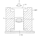
図1は、実施例1による光学素子の製造に用いるプレス成形型(金型)の構成を示すもので、成形用の下型1および上型2と、胴型3と、を有し、これらによって成形素材(光学材料)であるガラス素材4のプレス成形を行う。
FIG. 1 shows a configuration of a press mold (mold) used for manufacturing an optical element according to Example 1, which includes a lower mold 1 and an upper mold 2 for molding, and a
胴型3は、下型1と上型2の位置を規制し、支持するとともに、下型1および上型2を加熱するための図示しないヒーターを内部に備えている。
The
胴型3の内側表面(転写面)3aは、光軸方向の表面粗さRa(2)=0.5μm、円周方向の表面粗さRa(1)=0.08μmに加工されており、同等の表面粗さを成形品の側面部に転写するように構成されている。
The inner surface (transfer surface) 3a of the
このプレス成形型を用いて、光学素子を製造する方法について説明する。 A method for producing an optical element using this press mold will be described.
まず、胴型3、下型1および上型2、ガラス素材4が、胴型3に設けられたヒーターによって成形に必要な温度まで加熱される。
First, the
つぎに、上型2に対して、図示しないプレス軸より矢印Pで示す方向に荷重を加え、ガラス素材4をプレス成形する。ガラス素材4は上型2および下型1の転写面と、胴型3の内側表面3aを転写され、室温まで冷却することで成形を完了させる。
Next, a load is applied to the upper mold 2 in a direction indicated by an arrow P from a press shaft (not shown) to press-mold the
図2は成形された光学素子10を示すもので、光学有効部分の外側の非光学有効部分は、胴型3の内側表面3aを転写した外周面11を有する。
FIG. 2 shows the molded optical element 10, and the non-optically effective portion outside the optically effective portion has an outer
すなわち、光学素子10の外周面11には、胴型3の内側表面3aが転写され、胴型3の内側表面3aと同等に、光軸方向の表面粗さRa(2)=0.5μm、円周方向の表面粗さRa(1)=0.08μmであり、しかも光学材料は均一に充填されていた。
That is, the
このように粗面化された光学素子10の外周面11は、迷光を抑制するための黒色塗料を良好に塗布することが可能であった。光学素子10をレンズユニットに組み込み、その性能を評価したところ、ゴースト、フレア等の不具合がなく、外観形状も問題ない良品であることが確認できた。
The outer
本実施例において成形される光学材料はガラスであるが、これに限らず、プラスチックや金属であっても良い。 The optical material molded in this embodiment is glass, but is not limited to this, and may be plastic or metal.
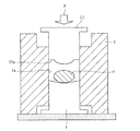
本実施例においては、実施例1の型構造の一部を変更し、凹メニス形状を成形する型構造である点だけが実施例1と異なる。他は実施例1と同様である。 The present embodiment is different from the first embodiment only in that it is a mold structure in which a part of the mold structure of the first embodiment is changed and a concave meniscus shape is formed. Others are the same as in the first embodiment.
図3は本実施例による光学素子の製造に用いるプレス成形型(金型)の構成を示す。実施例1の上型2の代わりに上駒22を用いる。上駒22は、非光学有効部分を転写するフラット部22aを有し、胴型3の内側表面3aと同様に、フラット部22aにおける径方向の表面粗さRa(2)=0.5μm、円周方向の表面粗さRa(1)=0.08μmである。
FIG. 3 shows the configuration of a press mold (mold) used for manufacturing the optical element according to this embodiment. The
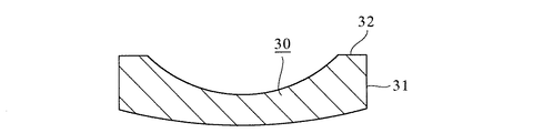
図4に示すように、成形品である光学素子30は、外周面31と上面側のフラット部32において上記のプレス成形型と同等の表面粗さを有する。
As shown in FIG. 4, the
光学素子30を実施例1と同様に評価したところ、良品であることが確認できた。
When the
(比較例)
実施例1と同様のプレス成形型において、胴型の内側表面の表面粗さが光軸方向にRa(2)=0.7μm、円周方向にRa(1)=0.009μm、0.01μm、0.5μm、0.6μmにそれぞれ加工された胴型サンプルS1〜S4を用意した。
(Comparative example)
In the same press mold as in Example 1, the surface roughness of the inner surface of the barrel die is Ra (2) = 0.7 μm in the optical axis direction, and Ra (1) = 0.09 μm, 0.01 μm in the circumferential direction. , 0.5 μm and 0.6 μm were prepared respectively.
胴型サンプルS1〜S4を用いてプレス成形した成形品である光学素子の評価を実施例1と同様に行った結果を表1に示す。判定は得られた光学素子が良品である場合を○、不良である場合を×とした。 Table 1 shows the results of evaluation of the optical element, which is a molded product press-molded using the barrel samples S1 to S4, in the same manner as in Example 1. In the determination, the case where the obtained optical element is a non-defective product was marked with ◯, and the case where it was defective was marked with ×.

表1より、Ra(1)が0.01μm以上、0.5μm以下であれば成形品が良品として得られることがわかる。 From Table 1, it can be seen that if Ra (1) is 0.01 μm or more and 0.5 μm or less, a molded product can be obtained as a good product.
また、同様に胴型の内側表面の表面粗さをRa(1)=0.01μm、Ra(2)=1.11μmとした胴型サンプルS5と、Ra(1)=0.01μm、Ra(2)=1μmとした胴型サンプルS6を用意した。また、Ra(1)=0.5μm、Ra(2)=0.625μmとした胴型サンプルS7と、Ra(1)=0.5μm、Ra(2)=0.555μmとした胴型サンプルS8を用意した。胴型サンプルS5〜S8を用いて、それぞれ実施例1と同様に成形および評価を行った。その結果を表2に示す。判定は得られた光学素子が良品である場合を○、不良である場合を×とした。 Similarly, a barrel sample S5 having a surface roughness Ra (1) = 0.01 μm and Ra (2) = 1.11 μm, and Ra (1) = 0.01 μm, Ra ( 2) A body sample S6 having a thickness of 1 μm was prepared. Also, a barrel sample S7 with Ra (1) = 0.5 μm and Ra (2) = 0.625 μm, and a barrel sample S8 with Ra (1) = 0.5 μm and Ra (2) = 0.555 μm. Prepared. Molding and evaluation were performed in the same manner as in Example 1 using the trunk samples S5 to S8. The results are shown in Table 2. In the determination, the case where the obtained optical element is a non-defective product was marked with ◯, and the case where it was defective was marked with ×.
表2より、Ra(1)/Ra(2)が0.01以上、0.8以下であれば成形品が良品となることがわかる。 From Table 2, it can be seen that if Ra (1) / Ra (2) is 0.01 or more and 0.8 or less, the molded product becomes a good product.
1 下型
2 上型
3 胴型
3a 内側表面
10 光学素子
22 上駒
22a フラット部
DESCRIPTION OF SYMBOLS 1 Lower mold | type 2 Upper mold |
Claims (4)
前記光学素子の非光学有効部分を成形する前記金型の転写面は、前記転写面の円周方向における表面粗さと、光軸方向または径方向における表面粗さとの間に以下の2式で表わされる関係が成立していることを特徴とする光学素子の製造方法。
0.01≦Ra(1)/Ra(2)≦0.8
0.01μm≦Ra(1)≦0.5μm
ここで、Ra(1):円周方向に測定した表面粗さRa
Ra(2):光軸方向または径方向に測定した表面粗さRa In the method of manufacturing an optical element that forms an optical element by molding using a mold composed of an upper mold, a lower mold, and a body mold,
The transfer surface of the mold for molding the non-optically effective portion of the optical element is expressed by the following two formulas between the surface roughness in the circumferential direction of the transfer surface and the surface roughness in the optical axis direction or radial direction. The manufacturing method of the optical element characterized by the above-mentioned relationship being materialized.
0.01 ≦ Ra (1) / Ra (2) ≦ 0.8
0.01 μm ≦ Ra (1) ≦ 0.5 μm
Here, Ra (1): surface roughness Ra measured in the circumferential direction
Ra (2): Surface roughness Ra measured in the optical axis direction or radial direction
0.01≦Ra(1)/Ra(2)≦0.8
0.01μm≦Ra(1)≦0.5μm
ここで、Ra(1):円周方向に測定した表面粗さRa
Ra(2):光軸方向または径方向に測定した表面粗さRa In an optical element formed by molding a molding material and having a non-optical effective portion outside the optical effective portion, the surface roughness in the circumferential direction of the non-optical effective portion and the surface in the optical axis direction or radial direction An optical element characterized in that a relationship represented by the following two expressions is established between the roughness and the roughness.
0.01 ≦ Ra (1) / Ra (2) ≦ 0.8
0.01 μm ≦ Ra (1) ≦ 0.5 μm
Here, Ra (1): surface roughness Ra measured in the circumferential direction
Ra (2): Surface roughness Ra measured in the optical axis direction or radial direction
0.01≦Ra(1)/Ra(2)≦0.8 0.01 ≦ Ra (1) / Ra (2) ≦ 0.8
0.01μm≦Ra(1)≦0.5μm 0.01 μm ≦ Ra (1) ≦ 0.5 μm
ここで、Ra(1):円周方向に測定した表面粗さRa Here, Ra (1): surface roughness Ra measured in the circumferential direction
Ra(2):光軸方向または径方向に測定した表面粗さRa Ra (2): Surface roughness Ra measured in the optical axis direction or radial direction
Priority Applications (1)
| Application Number | Priority Date | Filing Date | Title |
|---|---|---|---|
| JP2006278229A JP4777210B2 (en) | 2006-10-12 | 2006-10-12 | Optical element manufacturing method and optical element |
Applications Claiming Priority (1)
| Application Number | Priority Date | Filing Date | Title |
|---|---|---|---|
| JP2006278229A JP4777210B2 (en) | 2006-10-12 | 2006-10-12 | Optical element manufacturing method and optical element |
Publications (3)
| Publication Number | Publication Date |
|---|---|
| JP2008094658A JP2008094658A (en) | 2008-04-24 |
| JP2008094658A5 JP2008094658A5 (en) | 2009-11-26 |
| JP4777210B2 true JP4777210B2 (en) | 2011-09-21 |
Family
ID=39377892
Family Applications (1)
| Application Number | Title | Priority Date | Filing Date |
|---|---|---|---|
| JP2006278229A Active JP4777210B2 (en) | 2006-10-12 | 2006-10-12 | Optical element manufacturing method and optical element |
Country Status (1)
| Country | Link |
|---|---|
| JP (1) | JP4777210B2 (en) |
Families Citing this family (4)
| Publication number | Priority date | Publication date | Assignee | Title |
|---|---|---|---|---|
| US8390930B2 (en) | 2008-11-20 | 2013-03-05 | Omnivision Technologies, Inc. | Optical element and manufacture method thereof |
| WO2014050602A1 (en) * | 2012-09-29 | 2014-04-03 | コニカミノルタ株式会社 | Lens and molding die |
| JP6609422B2 (en) * | 2015-05-25 | 2019-11-20 | オリンパス株式会社 | Optical element molding die set and optical element manufacturing method |
| US11785323B1 (en) | 2022-05-27 | 2023-10-10 | Samsung Electronics Co., Ltd. | Camera module including refractive member and electronic device including refractive member |
Family Cites Families (3)
| Publication number | Priority date | Publication date | Assignee | Title |
|---|---|---|---|---|
| JPS6461328A (en) * | 1987-09-02 | 1989-03-08 | Olympus Optical Co | Glass lens and device for forming thereof |
| JP2001052333A (en) * | 1999-08-09 | 2001-02-23 | Fuji Electric Co Ltd | Plastic disk substrate of magnetic recording medium and metal mold for molding the same |
| JP2007296839A (en) * | 2006-04-06 | 2007-11-15 | Fuji Xerox Co Ltd | Cylindrical core body and method for manufacturing endless belt using cylindrical core body |
-
2006
- 2006-10-12 JP JP2006278229A patent/JP4777210B2/en active Active
Also Published As
| Publication number | Publication date |
|---|---|
| JP2008094658A (en) | 2008-04-24 |
Similar Documents
| Publication | Publication Date | Title |
|---|---|---|
| JP5963099B2 (en) | Plastic lens | |
| US6551530B2 (en) | Method of forming a hybrid lens | |
| JP2008175992A (en) | Optical element and optical unit | |
| JP4777210B2 (en) | Optical element manufacturing method and optical element | |
| JP2019120725A (en) | Lens unit and metal mold manufacturing method | |
| JP2009040642A (en) | Optical device and its manufacturing method | |
| US20050247081A1 (en) | Optical glass element and manufacturing method thereof | |
| US7764446B2 (en) | Bonded optical element | |
| JP2007304569A (en) | Compound lens and manufacture method thereof | |
| JP4949860B2 (en) | Manufacturing method of optical lens | |
| US20040196521A1 (en) | Method of manufacturing holder-mounted optical element | |
| JP4207819B2 (en) | Manufacturing method of aspherical optical element | |
| JP2019012112A (en) | Manufacturing method of plastic lens | |
| JP2008094658A5 (en) | ||
| WO2016051619A1 (en) | Optical lens | |
| JP2022162423A (en) | lens with barrel | |
| US20200132885A1 (en) | Optical element with antireflection structure, mold for manufacturing, method of manufacturing optical element with antireflection structure, and imaging apparatus | |
| WO2019189919A1 (en) | Optical element, optical system, and imaging apparatus | |
| JP4744352B2 (en) | Method for manufacturing composite optical element | |
| JP2007039262A (en) | Molded-type optical element and optical system having the same | |
| JP4168705B2 (en) | Optical element and mold for molding the same | |
| JP2007297229A (en) | Method for manufacturing optical device | |
| US8418516B2 (en) | Manufacturing method for optical element | |
| JP2011201739A (en) | Preform material for glass molding | |
| JP3230164B2 (en) | Glass molded lens and glass lens mold |
Legal Events
| Date | Code | Title | Description |
|---|---|---|---|
| RD03 | Notification of appointment of power of attorney |
Free format text: JAPANESE INTERMEDIATE CODE: A7423 Effective date: 20090527 |
|
| A521 | Written amendment |
Free format text: JAPANESE INTERMEDIATE CODE: A523 Effective date: 20091013 |
|
| A621 | Written request for application examination |
Free format text: JAPANESE INTERMEDIATE CODE: A621 Effective date: 20091013 |
|
| A977 | Report on retrieval |
Free format text: JAPANESE INTERMEDIATE CODE: A971007 Effective date: 20110328 |
|
| A131 | Notification of reasons for refusal |
Free format text: JAPANESE INTERMEDIATE CODE: A131 Effective date: 20110405 |
|
| A521 | Written amendment |
Free format text: JAPANESE INTERMEDIATE CODE: A523 Effective date: 20110602 |
|
| TRDD | Decision of grant or rejection written | ||
| A01 | Written decision to grant a patent or to grant a registration (utility model) |
Free format text: JAPANESE INTERMEDIATE CODE: A01 Effective date: 20110628 |
|
| A01 | Written decision to grant a patent or to grant a registration (utility model) |
Free format text: JAPANESE INTERMEDIATE CODE: A01 |
|
| A61 | First payment of annual fees (during grant procedure) |
Free format text: JAPANESE INTERMEDIATE CODE: A61 Effective date: 20110629 |
|
| R150 | Certificate of patent or registration of utility model |
Ref document number: 4777210 Country of ref document: JP Free format text: JAPANESE INTERMEDIATE CODE: R150 Free format text: JAPANESE INTERMEDIATE CODE: R150 |
|
| FPAY | Renewal fee payment (event date is renewal date of database) |
Free format text: PAYMENT UNTIL: 20140708 Year of fee payment: 3 |