JP4774635B2 - Thin film deposition apparatus for three-dimensional hollow container and thin film deposition method using the same - Google Patents
Thin film deposition apparatus for three-dimensional hollow container and thin film deposition method using the same Download PDFInfo
- Publication number
- JP4774635B2 JP4774635B2 JP2001181896A JP2001181896A JP4774635B2 JP 4774635 B2 JP4774635 B2 JP 4774635B2 JP 2001181896 A JP2001181896 A JP 2001181896A JP 2001181896 A JP2001181896 A JP 2001181896A JP 4774635 B2 JP4774635 B2 JP 4774635B2
- Authority
- JP
- Japan
- Prior art keywords
- container
- thin film
- external electrode
- dimensional hollow
- film deposition
- Prior art date
- Legal status (The legal status is an assumption and is not a legal conclusion. Google has not performed a legal analysis and makes no representation as to the accuracy of the status listed.)
- Expired - Fee Related
Links
Images


Landscapes
- Cartons (AREA)
- Details Of Rigid Or Semi-Rigid Containers (AREA)
- Chemical Vapour Deposition (AREA)
- Containers Having Bodies Formed In One Piece (AREA)
Description
【0001】
【発明の属する技術分野】
本発明は3次元中空容器、例えばプラスチックボトル、プラスチックカップ、プラスチックトレー、紙容器、紙カップ、紙トレー、その他中空のプラスチック成形品等の表面に化学蒸着法(CVD)により薄膜を形成するための薄膜成膜装置及びそれを用いた薄膜成膜方法に関する。
【0002】
【従来の技術】
近年、プラスチック容器等の3次元中空容器表面に機能性薄膜を成膜し、容器のガスバリア性、水蒸気バリア性、表面の濡れ性等を向上させる試みがなされている。これらの機能性薄膜を成膜する方法の一つとして、プラズマ助成式CVD法によるプロセスガスの化学反応により容器表面に薄膜を形成させる方法がある。この方法は、例えば特開平8−53117号公報に示されているように、容器の外形とほぼ相似形の中空状の外部電極と、容器の内形とほぼ相似形の内部電極の間に容器を設置し、薄膜を形成する方法であり、また特開平8−175528号公報に示されているように、外部電極、内部電極共に容器の表面からほぼ一定の距離に配置して薄膜を形成する方法である。しかしこれらの発明では、電極を容器の形状に合わせて作らなければならず、あらゆる形状の容器に対応できるものではなかった。
【0003】
【発明が解決しようとする課題】
本発明は上記従来技術の問題点を解決するためになされたもので、装置に大きな変更を加えることなく、必要最低限の変更で様々な形状の容器への薄膜形成に対応できる薄膜成膜装置及びそれを用いた薄膜成膜方法を提供することを目的とする。
【0004】
本発明は、以上の目的を達成すべくなされたもので、請求項1に記載の発明は、成膜チャンバーが、内部に容器が収容できるだけの円筒状のスペースを持つ筒体と、その筒体の片方の開口端に設置される天蓋と、もう一方の開口端に設置され排気口を持つ底蓋とよりなり、成膜チャンバー内には薄膜を形成しようとする容器を所定位置に保持するための容器保持部品が、筒体の側壁と容器の間には導電性材料よりなる外部電極がそれぞれ設置され、内部電極は底蓋を通して容器保持部品に保持される容器内部に位置するように挿入されていると共に、外部電極と容器保持部品とは薄膜を形成しようとする容器に合ったものに適宜交換可能になっていることを特徴とする3次元中空容器への薄膜成膜装置である。
【0005】
また、請求項2に記載の発明は、請求項1に記載の3次元中空容器への薄膜成膜装置において、外部電極と容器の間に外部電極と接触するように絶縁性材料からなるスペーサーが挿入されていることを特徴とする。
【0006】
さらにまた、請求項3に記載の発明は、請求項2に記載の3次元中空容器への薄膜成膜装置において、絶縁性材料からなるスペーサーがプラスチックであることを特徴とする。
【0007】
さらにまた、請求項4に記載の発明は、請求項1ないし請求項3のいずれか1項に記載の3次元中空容器への薄膜成膜装置において、底蓋が導電性材料よりなり、かつ筒体の側壁と底蓋の間に絶縁体よりなる絶縁板が介在されていることを特徴とする。
【0008】
さらにまた、請求項5に記載の発明は、請求項1ないし請求項4のいずれか1項に記載の3次元中空容器への薄膜成膜装置において、筒体、天蓋及び底蓋よりなる成膜チャンバー内に容器を保持する絶縁体よりなる容器保持部品が設置されていることを特徴する。
【0009】
さらにまた、請求項6に記載の発明は、請求項1ないし請求項5のいずれか1項に記載の3次元中空容器への薄膜成膜装置において、内部電極の先端にガス吐出口として直径0.5mm以下の穴が少なくとも1つ以上開いていることを特徴とする。
【0010】
さらにまた、請求項7に記載の発明は、請求項1ないし請求項5のいずれか1項に記載の3次元中空容器への薄膜成膜装置において、内部電極の先端にガス吐出口として短径が0.5mm以下の長穴が少なくとも1つ以上開いていることを特徴とする。
【0011】
さらにまた、請求項8に記載の発明は、3次元中空容器の表面にCVD法により薄膜を形成させる方法であり、内部に薄膜を形成させる容器が収容できるだけの円筒状のスペースを持つ筒体と、その筒体の片方の開口端に設置される天蓋と、もう一方の開口端に設置され排気口を持つ底蓋とよりなる成膜チャンバー内に、薄膜を形成しようとする容器に適合するようにして選択した容器保持部品を設置させ、この容器保持部品により容器を所定位置で保持する一方、筒体の側壁と容器の間には容器に適合するようにして選択した導電性材料よりなる外部電極を設置させると共に、容器内部には内部電極を設置させ、しかる後、底蓋に設置された排気口を介して容器内部を含む成膜チャンバー内を真空にし、続いて底蓋を通して容器内部に挿入されている内部電極の先端よりプロセスガスを容器内に導入し、外部電極と内部電極間に高周波またはマイクロ波電力をかけ、プロセスガスをプラズマ化することにより容器表面に薄膜を形成することを特徴とする。
【0012】
【発明の実施の形態】
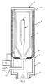
以下、本発明の薄膜成膜装置を、一実施形態に係る断面構成の概略を示す図1を用いて説明する。
図1に示す薄膜成膜装置は、成膜チャンバーが、内部に薄膜を形成しようとする容器1が収容できるだけの円筒状のスペースを持つ筒体2と、その筒体2の片方の開口端に設置される天蓋3と、もう一方の開口端に設置され排気口5を持つ底蓋6とよりなり、成膜チャンバー内には薄膜を形成しようとする容器1を所定位置に保持するための容器保持部品10が、筒体2の側壁と容器1の間には導電性材料よりなる外部電極4がそれぞれ設置され、内部電極7は成膜チャンバーの底蓋6を通して容器保持部品10に保持されている容器1の内部に位置するように設置されていると共に、外部電極4と容器保持部品10とは薄膜を形成しようとする容器1に合ったものに適宜交換可能になっている
【0013】
この装置の重要な特徴の一つは、筒体2がその内部に薄膜を形成しようとする容器1を収納できるだけの円筒状のスペースを有していることである。筒体2の内部を円筒状とすることにより、筒体2の製造が容易となり、かつ安価に製造できるという効果を奏する。筒体2は、内部のスペースが円筒状であれば良く、外側の形状に特に制限はない。また、筒体2の材質としては特に制限はないが、ガラス、プラスチック等の絶縁性材料が好適である。
【0014】
二つ目の重要な特徴は、導電性材料よりなる外部電極4が筒体2の側壁と容器1の間に設置されていると共に、薄膜を形成する容器に合わせたものに適宜交換できるようになっていることである。
容器2の内表面へ均一な薄膜を成膜するためには外部電極4と内部電極7は容器1を挟んで対向するように設置されなければならず、かつ外部電極4は容器1の長さ(高さ)とほぼ等しいことが望ましい。すなわち、容器の長さに対して著しく長い外部電極を使用すると、容器の無い部分に密度の高いプラズマが発生し、結果として容器内部に適切なプラズマを発生させることが困難となる。したがって、本発明の薄膜成膜装置では導電性材料よりなる外部電極4を筒体2の側壁と容器1の間に設置し、かつその外部電極4は容器1の長さに合ったものに適宜交換できるようにすることで、さまざまな容器に対して均質な薄膜の形成を可能にしている。さらに、この外部電極4は簡単に脱着可能なことが望ましい。
【0015】
一方、本発明に係る薄膜成膜装置においては、図2に示したように、導電性材料よりなる外部電極4と容器1の間に外部電極4と接触するように絶縁性材料からなるスペーサー8を挿入できるようにもなっている。このスペーサー8を薄膜を形成しようとする容器のサイズに合わせて変更することにより、サイズの異なる容器でも同一の真空装置を用いることができる。すなわち、小さいサイズの容器に成膜する場合には、厚いスペーサーを用い成膜チャンバー内部のスペースを小さくすることで、真空チャンバー内部を真空にする時間が短縮でき、かつ容器は外部電極の中心に配置されるため、薄膜の厚みを均一にするためにも好ましい。また例えば楕円形状の断面を有する容器でもスペーサーの外側は外部電極に合うように円形に、内側は容器形状に合わせて楕円形状にすることで均一な厚みの成膜が可能となる。また、スペーサーを用いない場合、成膜を繰り返すうちに外部電極の表面がプロセスガス等により汚染され放電効率が低下する場合がある。したがって、前記スペーサーを用いることにより外部電極の汚れを防止でき、長期間にわたり安定した成膜が可能となる。スペーサーの材質としては、加工の容易性および表面が汚染されたとしても放電効率に影響を及ぼさない絶縁材料、特にプラスチックが好ましい。以上の理由により、このスペーサーは外部電極と接触するように挿入され、かつ容易な脱着が可能であることが好ましい。
【0016】
三つ目の特徴は、成膜チャンバーの天蓋3とは反対側に排気口5を有する底蓋6が設置されていることである。
成膜チャンバー内には内部を真空にするため、この排気口5を通して真空ポンプ(図示せず)が設置されている。また、底蓋6の材質には特に制限は無いが、機械的強度等の面より金属が好ましい。しかし、金属のような導電性材料を用いた場合には、底蓋6と外部電極4の間に絶縁板9を介在させることが好ましい。また、容器1を成膜チャンバーの適正な位置に配置するため図1に示すような絶縁体9よりなる容器保持部品10を成膜チャンバー内に設置することが望ましい。さらに、この容器保持部品10と絶縁板9を一体の部品とすることで、装置部品点数を減らすことも可能である。
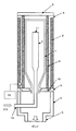
【0017】
一方、図3には、図1の容器1とは長さ(高さ)の異なる容器31に均質な薄膜を形成するように図1に示す薄膜成膜装置の外部電極4と容器保持部品10に代わって外部電極34と容器保持部品30を交換したときの装置の状態が示してある。容器の長さが変更になったのに対応して、簡単に脱着可能な外部電極34と、容器保持部品30の2点の部品だけを変更することで容器31に対して均質な薄膜の形成が可能となる。
【0018】
本発明の薄膜成膜装置は以上のような構成であるが、以下にこの装置を用いた薄膜成膜方法を図1を参照して説明する。
まず、内部に薄膜を形成しようとする容器1が収容できるだけの円筒状のスペースを持つ筒体2と、その筒体2の片方の開口端に設置される天蓋3と、もう一方の開口端に設置され排気口5を持つ底蓋6とよりなる成膜チャンバー内に、容器1に適合するように選択して設置させた容器保持部品10により容器1を所定位置で保持する一方、筒体2の側壁と容器1の間には容器に適合するように適宜選択した導電性材料よりなる外部電極4を設置させると共に、容器1の内部には内部電極7を設置させ、しかる後、底蓋6に設置された排気口5を介して容器1の内部を含む成膜チャンバー内を真空にし、続いて底蓋6を通して容器1の内部に挿入されている内部電極7の先端よりプロセスガスを容器1内に導入し、外部電極4と内部電極7間に高周波またはマイクロ波電力をかけ、プロセスガスをプラズマ化することにより容器1の内表面に薄膜を形成する。
【0019】
プロセスガスは、中空管となっている内部電極7の先端のガス吐出口11より容器1の内部に供給する。この場合、先端のガス吐出口11が大きすぎるとプロセスガスが内部電極7の内部でプラズマ化し、化学反応が進むため、結果として容器1に形成される薄膜の厚みがガス吐出口11付近では厚くなり、逆にガス吐出口11から遠い部分では薄くなってしまう。したがって、ガス吐出口11は図4に示すように少なくとも一つ以上の直径0.5mm以下の穴もしくは短径が0.5mm以下の長穴とすることが望ましい。
【0020】
【実施例】
以下、本発明の実施例を説明する。
<実施例1>
図1に示すような薄膜成膜装置、すなわち成膜チャンバーが、内部に容器が収容できるだけの円筒状のスペースを持つ筒体2と、その筒体2の片方の開口端に設置される天蓋3と、もう一方の開口端に設置され排気口5を持つ底蓋6とよりなり、成膜チャンバー内には薄膜を形成しようとする容器1を所定位置に保持するための容器保持部品10が、筒体2の側壁と容器1の間には導電性材料よりなる外部電極4がそれぞれ設置され、内部電極7は底蓋6を通して容器保持部品10に保持される容器1の内部に位置するように設置されていると共に、外部電極4と容器保持部品10とは薄膜を形成しようとする容器に合ったものに適宜交換可能になっている薄膜成膜装置を用いて、容量が500mlで長さ(高さ)が20cmのポリエチレンテレフタレート製容器の内表面に酸化珪素薄膜の成膜を行った。
【0021】
用いたプロセスガスはヘキサメチルジシロキサンと酸素の混合ガスであり、それぞれの流量は10sccmと500sccmであった。この混合ガスを先端に直径が0.5mmのガス吐出口11を有する内部電極7を通して、容器保持部品10により成膜チャンバーの所定位置に設置した容器1内に導入し、成膜時圧力66.5Pa、印可電力200wattで15秒間高周波を印可し、成膜を行った。
容器1内部には酸化珪素の薄膜が成膜され、膜厚もほぼ均一であった。
【0022】
<実施例2>
図3示すような薄膜成膜装置を用いて、実施例1で用いた容器とは長さの異なる容器31(長さ31cm)の内表面へ酸化珪素薄膜の成膜を行った。
まず、薄膜の形成に先立ち、装置内に予め設置してあった外部電極と容器保持部品を薄膜を形成しようとする容器31の大きさならびに高さに適合する外部電極34と容器保持部品30に交換した。
用いたプロセスガスはヘキサメチルジシロキサンと酸素の混合ガスであり、それぞれの流量は10sccmと500sccmであった。この混合ガスを内部電極7の先端に設けられ、短径が0.5mmの長穴を有する図4のaに示すようなガス吐出口11を通して容器31の内部に供給し、成膜時圧力66.5Pa、印可電力200wattで15秒間高周波を印可し、成膜を行った。
容器31の内部には酸化珪素の薄膜が成膜され、膜厚もほぼ均一であった。
【0023】
【発明の効果】
以上のような本発明は、装置に大きな変更を加えることなく、様々な形態の容器への薄膜形成に対応することが可能となる。
すなわち、外部電極と容器保持部品を薄膜を形成しようとする容器に合わせて選択して設置することにより、様々な容器に対して均質な薄膜の形成が可能となる。また、外部電極と容器の間に外部電極と接触するようにして絶縁性材料からなるスペーサーを薄膜を形成しようとする容器のサイズに合わせて挿入、設置することにより、均質な薄膜を効率良く形成できると共に、外部電極の汚れを防止することができ、長期間に渡り安定した成膜が可能となる。
【図面の簡単な説明】
【図1】本発明の一実施形態に係る薄膜成膜装置の概略断面構成説明図である。
【図2】本発明の他の実施形態に係る薄膜成膜装置の概略断面構成説明図である。
【図3】本発明のさらに他の実施形態に係る薄膜成膜装置の概略断面構成説明図である。
【図4】ガス吐出口の平面構成説明図である。
【符号の説明】
1・・・容器
2・・・筒体
3・・・天蓋
4・・・外部電極
5・・・排気口
6・・・底蓋
7・・・内部電極
8・・・スペーサー
9・・・絶縁板
10・・・容器保持部品
11・・・ガス吐出口
14・・・プロセスガス供給管
15・・・高周波電源[0001]
BACKGROUND OF THE INVENTION
The present invention is a thin film for forming a thin film on the surface of a three-dimensional hollow container such as a plastic bottle, a plastic cup, a plastic tray, a paper container, a paper cup, a paper tray, and other hollow plastic molded articles by chemical vapor deposition (CVD). The present invention relates to a film forming apparatus and a thin film forming method using the same.
[0002]
[Prior art]
In recent years, attempts have been made to improve the gas barrier property, water vapor barrier property, surface wettability, and the like of a container by forming a functional thin film on the surface of a three-dimensional hollow container such as a plastic container. As one of methods for forming these functional thin films, there is a method of forming a thin film on the surface of a container by a chemical reaction of a process gas by a plasma assisted CVD method. In this method, for example, as disclosed in Japanese Patent Laid-Open No. 8-53117, a container is formed between a hollow external electrode that is substantially similar to the outer shape of the container and an internal electrode that is approximately similar to the inner shape of the container. The thin film is formed by arranging both the external electrode and the internal electrode at a substantially constant distance from the surface of the container as disclosed in JP-A-8-175528. Is the method. However, in these inventions, the electrodes must be made in accordance with the shape of the container, and cannot be applied to containers of all shapes.
[0003]
[Problems to be solved by the invention]
The present invention has been made to solve the above-mentioned problems of the prior art, and is a thin film deposition apparatus capable of forming thin films in various shapes of containers with minimal changes without adding a major change to the apparatus. Another object of the present invention is to provide a method for forming a thin film using the same.
[0004]
The present invention has been made to achieve the above object, and in the invention described in
[0005]
The invention described in
[0006]
Furthermore, the invention described in
[0007]
Furthermore, the invention described in
[0008]
Furthermore, the invention according to
[0009]
Furthermore, the invention according to
[0010]
Furthermore, the invention according to claim 7 is the thin film deposition apparatus for the three-dimensional hollow container according to any one of
[0011]
Furthermore, the invention described in
[0012]
DETAILED DESCRIPTION OF THE INVENTION
Hereinafter, a thin film deposition apparatus of the present invention will be described with reference to FIG. 1 showing an outline of a cross-sectional configuration according to an embodiment.
In the thin film deposition apparatus shown in FIG. 1, a deposition chamber has a
One of the important features of this apparatus is that the
[0014]
The second important feature is that the
In order to form a uniform thin film on the inner surface of the
[0015]
On the other hand, in the thin film deposition apparatus according to the present invention, as shown in FIG. 2, the
[0016]
The third feature is that a
In order to evacuate the inside of the film forming chamber, a vacuum pump (not shown) is installed through the
[0017]
On the other hand, FIG. 3 shows the
[0018]
The thin film deposition apparatus of the present invention is configured as described above, and a thin film deposition method using this apparatus will be described below with reference to FIG.
First, a
[0019]
The process gas is supplied into the
[0020]
【Example】
Examples of the present invention will be described below.
<Example 1>
A thin film deposition apparatus as shown in FIG. 1, that is, a film deposition chamber, has a
[0021]
The process gas used was a mixed gas of hexamethyldisiloxane and oxygen, and the respective flow rates were 10 sccm and 500 sccm. This mixed gas is introduced into the
A thin film of silicon oxide was formed inside the
[0022]
<Example 2>
Using a thin film deposition apparatus as shown in FIG. 3, a silicon oxide thin film was deposited on the inner surface of a container 31 (
First, prior to the formation of the thin film, the external electrode and the
The process gas used was a mixed gas of hexamethyldisiloxane and oxygen, and the respective flow rates were 10 sccm and 500 sccm. This mixed gas is supplied to the inside of the
A thin film of silicon oxide was formed inside the
[0023]
【The invention's effect】
The present invention as described above can cope with the formation of thin films in various types of containers without greatly changing the apparatus.
That is, by selecting and installing the external electrode and the container holding component in accordance with the container on which the thin film is to be formed, it is possible to form a uniform thin film for various containers. A homogeneous thin film can be efficiently formed by inserting and installing a spacer made of an insulating material in contact with the external electrode between the external electrode and the container in accordance with the size of the container on which the thin film is to be formed. In addition, contamination of the external electrode can be prevented, and stable film formation can be achieved over a long period of time.
[Brief description of the drawings]
FIG. 1 is a schematic cross-sectional configuration explanatory diagram of a thin film deposition apparatus according to an embodiment of the present invention.
FIG. 2 is a schematic cross-sectional configuration explanatory diagram of a thin film deposition apparatus according to another embodiment of the present invention.
FIG. 3 is a schematic cross-sectional configuration explanatory diagram of a thin film deposition apparatus according to still another embodiment of the present invention.
FIG. 4 is an explanatory diagram of a planar configuration of a gas discharge port.
[Explanation of symbols]
DESCRIPTION OF
Claims (8)
Priority Applications (1)
| Application Number | Priority Date | Filing Date | Title |
|---|---|---|---|
| JP2001181896A JP4774635B2 (en) | 2001-06-15 | 2001-06-15 | Thin film deposition apparatus for three-dimensional hollow container and thin film deposition method using the same |
Applications Claiming Priority (1)
| Application Number | Priority Date | Filing Date | Title |
|---|---|---|---|
| JP2001181896A JP4774635B2 (en) | 2001-06-15 | 2001-06-15 | Thin film deposition apparatus for three-dimensional hollow container and thin film deposition method using the same |
Publications (2)
| Publication Number | Publication Date |
|---|---|
| JP2002371364A JP2002371364A (en) | 2002-12-26 |
| JP4774635B2 true JP4774635B2 (en) | 2011-09-14 |
Family
ID=19022095
Family Applications (1)
| Application Number | Title | Priority Date | Filing Date |
|---|---|---|---|
| JP2001181896A Expired - Fee Related JP4774635B2 (en) | 2001-06-15 | 2001-06-15 | Thin film deposition apparatus for three-dimensional hollow container and thin film deposition method using the same |
Country Status (1)
| Country | Link |
|---|---|
| JP (1) | JP4774635B2 (en) |
Families Citing this family (24)
| Publication number | Priority date | Publication date | Assignee | Title |
|---|---|---|---|---|
| JP2005105294A (en) * | 2003-09-26 | 2005-04-21 | Mitsubishi Shoji Plast Kk | CVD film forming apparatus and CVD film coated plastic container manufacturing method |
| JP2005113202A (en) * | 2003-10-08 | 2005-04-28 | Mitsubishi Shoji Plast Kk | Plasma cvd film deposition system |
| JP4664658B2 (en) * | 2004-12-02 | 2011-04-06 | 麒麟麦酒株式会社 | Plasma CVD film forming apparatus and method for manufacturing plastic container having gas barrier property |
| JP5083500B2 (en) * | 2006-11-28 | 2012-11-28 | 凸版印刷株式会社 | Plastic container deposition equipment |
| MX350703B (en) | 2009-05-13 | 2017-09-14 | Sio2 Medical Products Inc | Outgassing method for inspecting a coated surface. |
| US7985188B2 (en) | 2009-05-13 | 2011-07-26 | Cv Holdings Llc | Vessel, coating, inspection and processing apparatus |
| WO2013170052A1 (en) | 2012-05-09 | 2013-11-14 | Sio2 Medical Products, Inc. | Saccharide protective coating for pharmaceutical package |
| US9458536B2 (en) | 2009-07-02 | 2016-10-04 | Sio2 Medical Products, Inc. | PECVD coating methods for capped syringes, cartridges and other articles |
| US11624115B2 (en) | 2010-05-12 | 2023-04-11 | Sio2 Medical Products, Inc. | Syringe with PECVD lubrication |
| US9878101B2 (en) | 2010-11-12 | 2018-01-30 | Sio2 Medical Products, Inc. | Cyclic olefin polymer vessels and vessel coating methods |
| US9272095B2 (en) | 2011-04-01 | 2016-03-01 | Sio2 Medical Products, Inc. | Vessels, contact surfaces, and coating and inspection apparatus and methods |
| EP2776603B1 (en) | 2011-11-11 | 2019-03-06 | SiO2 Medical Products, Inc. | PASSIVATION, pH PROTECTIVE OR LUBRICITY COATING FOR PHARMACEUTICAL PACKAGE, COATING PROCESS AND APPARATUS |
| US11116695B2 (en) | 2011-11-11 | 2021-09-14 | Sio2 Medical Products, Inc. | Blood sample collection tube |
| US20150297800A1 (en) | 2012-07-03 | 2015-10-22 | Sio2 Medical Products, Inc. | SiOx BARRIER FOR PHARMACEUTICAL PACKAGE AND COATING PROCESS |
| CA2890066C (en) | 2012-11-01 | 2021-11-09 | Sio2 Medical Products, Inc. | Coating inspection method |
| US9903782B2 (en) | 2012-11-16 | 2018-02-27 | Sio2 Medical Products, Inc. | Method and apparatus for detecting rapid barrier coating integrity characteristics |
| US9764093B2 (en) | 2012-11-30 | 2017-09-19 | Sio2 Medical Products, Inc. | Controlling the uniformity of PECVD deposition |
| JP6382830B2 (en) | 2012-11-30 | 2018-08-29 | エスアイオーツー・メディカル・プロダクツ・インコーポレイテッド | Uniformity control of PECVD deposition on medical syringes, cartridges, etc. |
| US9662450B2 (en) | 2013-03-01 | 2017-05-30 | Sio2 Medical Products, Inc. | Plasma or CVD pre-treatment for lubricated pharmaceutical package, coating process and apparatus |
| US9937099B2 (en) | 2013-03-11 | 2018-04-10 | Sio2 Medical Products, Inc. | Trilayer coated pharmaceutical packaging with low oxygen transmission rate |
| EP2971228B1 (en) | 2013-03-11 | 2023-06-21 | Si02 Medical Products, Inc. | Coated packaging |
| US20160017490A1 (en) | 2013-03-15 | 2016-01-21 | Sio2 Medical Products, Inc. | Coating method |
| WO2015148471A1 (en) | 2014-03-28 | 2015-10-01 | Sio2 Medical Products, Inc. | Antistatic coatings for plastic vessels |
| EP3337915B1 (en) | 2015-08-18 | 2021-11-03 | SiO2 Medical Products, Inc. | Pharmaceutical and other packaging with low oxygen transmission rate |
Family Cites Families (3)
| Publication number | Priority date | Publication date | Assignee | Title |
|---|---|---|---|---|
| JP4089066B2 (en) * | 1999-02-10 | 2008-05-21 | 凸版印刷株式会社 | Film forming apparatus and film forming method |
| JP3870598B2 (en) * | 1999-03-04 | 2007-01-17 | 凸版印刷株式会社 | Plastic container deposition equipment |
| JP3925025B2 (en) * | 2000-02-01 | 2007-06-06 | 凸版印刷株式会社 | Film forming apparatus and film forming method |
-
2001
- 2001-06-15 JP JP2001181896A patent/JP4774635B2/en not_active Expired - Fee Related
Also Published As
| Publication number | Publication date |
|---|---|
| JP2002371364A (en) | 2002-12-26 |
Similar Documents
| Publication | Publication Date | Title |
|---|---|---|
| JP4774635B2 (en) | Thin film deposition apparatus for three-dimensional hollow container and thin film deposition method using the same | |
| JP4168671B2 (en) | Thin film deposition system for 3D hollow containers | |
| JP4385657B2 (en) | Film forming apparatus and film forming method | |
| JP2003054532A (en) | Chemical plasma processing method for container inner surface | |
| WO2003085165A1 (en) | Plasma cvd film forming apparatus and method for manufacturing cvd film coating plastic container | |
| CN100453695C (en) | Microwave plasma processing apparatus | |
| JP4664658B2 (en) | Plasma CVD film forming apparatus and method for manufacturing plastic container having gas barrier property | |
| JP5610345B2 (en) | Manufacturing method of plastic container having gas barrier property, adapter for small container and thin film deposition apparatus | |
| WO2003000559A1 (en) | Manufacturing device for dlc film coated plastic container, dlc film coated plastic container, and method of manufacturing the dlc film coated plastic container | |
| CN100447297C (en) | Microwave plasma treatment method | |
| JP3870598B2 (en) | Plastic container deposition equipment | |
| JP3925025B2 (en) | Film forming apparatus and film forming method | |
| JPWO2002085717A1 (en) | Gas-barrier synthetic resin container, apparatus for producing the same, and article-containing gas-barrier synthetic resin container | |
| WO2005035825A1 (en) | Cvd film-forming device and method of manufacturing cvd film coating plastic container | |
| JP3880797B2 (en) | Diamond-like carbon film deposition equipment | |
| JP4380185B2 (en) | Chemical plasma treatment method for inner surface of plastic bottle | |
| JP4826042B2 (en) | Film forming apparatus and film forming method for cup-shaped container | |
| JP2005113202A (en) | Plasma cvd film deposition system | |
| JP4794800B2 (en) | Thin film deposition method and thin film deposition apparatus | |
| WO2003000558A1 (en) | Moisture and gas barrier plastic container with partition plates, and device and method for manufacturing the plastic container | |
| JP2009221490A (en) | Film-forming apparatus for hollow container | |
| JP2005015872A (en) | Film forming apparatus and film forming method | |
| JP2003138379A (en) | Film forming equipment | |
| JP2006124739A (en) | Plasma CVD deposition system | |
| JP2006307346A (en) | Thin film deposition method and thin film deposition apparatus |
Legal Events
| Date | Code | Title | Description |
|---|---|---|---|
| A621 | Written request for application examination |
Free format text: JAPANESE INTERMEDIATE CODE: A621 Effective date: 20080522 |
|
| A977 | Report on retrieval |
Free format text: JAPANESE INTERMEDIATE CODE: A971007 Effective date: 20101008 |
|
| TRDD | Decision of grant or rejection written | ||
| A01 | Written decision to grant a patent or to grant a registration (utility model) |
Free format text: JAPANESE INTERMEDIATE CODE: A01 Effective date: 20110531 |
|
| A01 | Written decision to grant a patent or to grant a registration (utility model) |
Free format text: JAPANESE INTERMEDIATE CODE: A01 |
|
| A61 | First payment of annual fees (during grant procedure) |
Free format text: JAPANESE INTERMEDIATE CODE: A61 Effective date: 20110613 |
|
| R150 | Certificate of patent or registration of utility model |
Free format text: JAPANESE INTERMEDIATE CODE: R150 Ref document number: 4774635 Country of ref document: JP Free format text: JAPANESE INTERMEDIATE CODE: R150 |
|
| FPAY | Renewal fee payment (event date is renewal date of database) |
Free format text: PAYMENT UNTIL: 20140708 Year of fee payment: 3 |
|
| LAPS | Cancellation because of no payment of annual fees |